Embed Size (px)
Citation preview

Subscriber access provided by - Access paid by the | UC Irvine Libraries
Nano Letters is published by the American Chemical Society. 1155 SixteenthStreet N.W., Washington, DC 20036
Letter
Coupled Electrooxidation and ElectricalConduction in a Single Gold Nanowire
Chengxiang Xiang, Aleix G. Gu#ell, Matthew A. Brown, JungYun Kim, John C. Hemminger, and Reginald M. Penner
Nano Lett., 2008, 8 (9), 3017-3022 • DOI: 10.1021/nl8021175 • Publication Date (Web): 20 August 2008
Downloaded from http://pubs.acs.org on December 7, 2008
More About This Article
Additional resources and features associated with this article are available within the HTML version:
• Supporting Information• Access to high resolution figures• Links to articles and content related to this article• Copyright permission to reproduce figures and/or text from this article
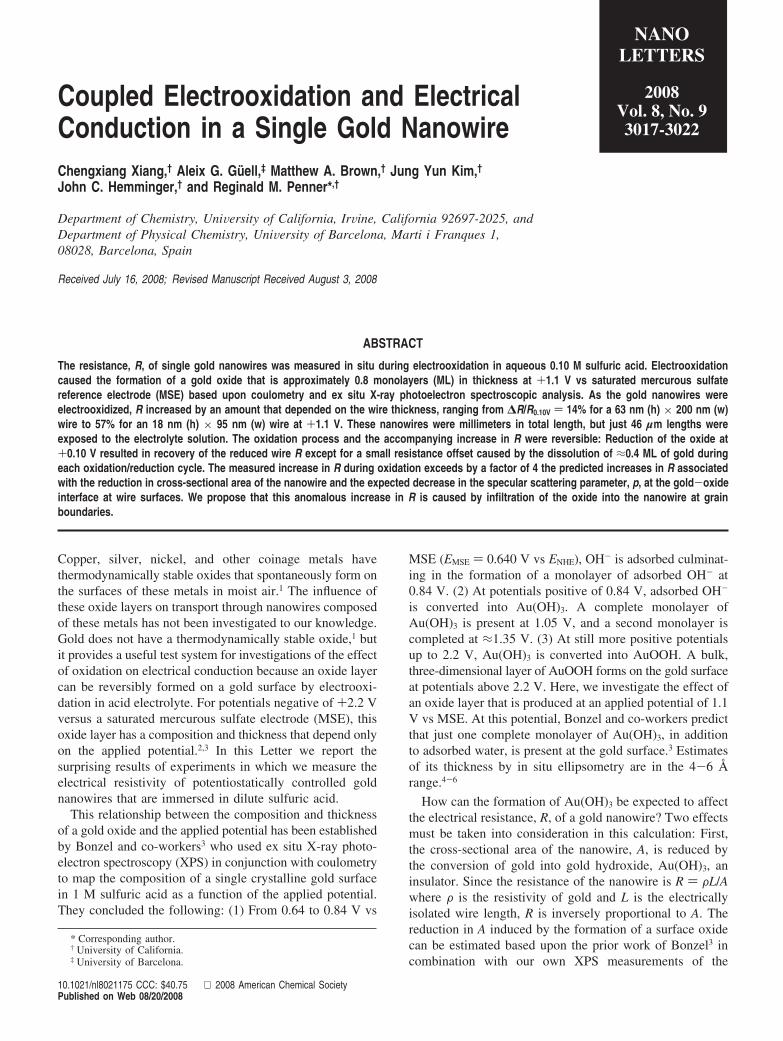
Coupled Electrooxidation and ElectricalConduction in a Single Gold NanowireChengxiang Xiang,† Aleix G. Guell,‡ Matthew A. Brown,† Jung Yun Kim,†John C. Hemminger,† and Reginald M. Penner*,†
Department of Chemistry, UniVersity of California, IrVine, California 92697-2025, andDepartment of Physical Chemistry, UniVersity of Barcelona, Marti i Franques 1,08028, Barcelona, Spain
Received July 16, 2008; Revised Manuscript Received August 3, 2008
ABSTRACT
The resistance, R, of single gold nanowires was measured in situ during electrooxidation in aqueous 0.10 M sulfuric acid. Electrooxidationcaused the formation of a gold oxide that is approximately 0.8 monolayers (ML) in thickness at +1.1 V vs saturated mercurous sulfatereference electrode (MSE) based upon coulometry and ex situ X-ray photoelectron spectroscopic analysis. As the gold nanowires wereelectrooxidized, R increased by an amount that depended on the wire thickness, ranging from ∆R/R0.10V ) 14% for a 63 nm (h) × 200 nm (w)wire to 57% for an 18 nm (h) × 95 nm (w) wire at +1.1 V. These nanowires were millimeters in total length, but just 46 µm lengths wereexposed to the electrolyte solution. The oxidation process and the accompanying increase in R were reversible: Reduction of the oxide at+0.10 V resulted in recovery of the reduced wire R except for a small resistance offset caused by the dissolution of ≈0.4 ML of gold duringeach oxidation/reduction cycle. The measured increase in R during oxidation exceeds by a factor of 4 the predicted increases in R associatedwith the reduction in cross-sectional area of the nanowire and the expected decrease in the specular scattering parameter, p, at the gold-oxideinterface at wire surfaces. We propose that this anomalous increase in R is caused by infiltration of the oxide into the nanowire at grainboundaries.
Copper, silver, nickel, and other coinage metals havethermodynamically stable oxides that spontaneously form onthe surfaces of these metals in moist air.1 The influence ofthese oxide layers on transport through nanowires composedof these metals has not been investigated to our knowledge.Gold does not have a thermodynamically stable oxide,1 butit provides a useful test system for investigations of the effectof oxidation on electrical conduction because an oxide layercan be reversibly formed on a gold surface by electrooxi-dation in acid electrolyte. For potentials negative of +2.2 Vversus a saturated mercurous sulfate electrode (MSE), thisoxide layer has a composition and thickness that depend onlyon the applied potential.2,3 In this Letter we report thesurprising results of experiments in which we measure theelectrical resistivity of potentiostatically controlled goldnanowires that are immersed in dilute sulfuric acid.
This relationship between the composition and thicknessof a gold oxide and the applied potential has been establishedby Bonzel and co-workers3 who used ex situ X-ray photo-electron spectroscopy (XPS) in conjunction with coulometryto map the composition of a single crystalline gold surfacein 1 M sulfuric acid as a function of the applied potential.They concluded the following: (1) From 0.64 to 0.84 V vs
MSE (EMSE ) 0.640 V vs ENHE), OH- is adsorbed culminat-ing in the formation of a monolayer of adsorbed OH- at0.84 V. (2) At potentials positive of 0.84 V, adsorbed OH-
is converted into Au(OH)3. A complete monolayer ofAu(OH)3 is present at 1.05 V, and a second monolayer iscompleted at ≈1.35 V. (3) At still more positive potentialsup to 2.2 V, Au(OH)3 is converted into AuOOH. A bulk,three-dimensional layer of AuOOH forms on the gold surfaceat potentials above 2.2 V. Here, we investigate the effect ofan oxide layer that is produced at an applied potential of 1.1V vs MSE. At this potential, Bonzel and co-workers predictthat just one complete monolayer of Au(OH)3, in additionto adsorbed water, is present at the gold surface.3 Estimatesof its thickness by in situ ellipsometry are in the 4-6 Årange.4-6
How can the formation of Au(OH)3 be expected to affectthe electrical resistance, R, of a gold nanowire? Two effectsmust be taken into consideration in this calculation: First,the cross-sectional area of the nanowire, A, is reduced bythe conversion of gold into gold hydroxide, Au(OH)3, aninsulator. Since the resistance of the nanowire is R ) FL/Awhere F is the resistivity of gold and L is the electricallyisolated wire length, R is inversely proportional to A. Thereduction in A induced by the formation of a surface oxidecan be estimated based upon the prior work of Bonzel3 incombination with our own XPS measurements of the
* Corresponding author.† University of California.‡ University of Barcelona.
NANOLETTERS
2008Vol. 8, No. 93017-3022
10.1021/nl8021175 CCC: $40.75 2008 American Chemical SocietyPublished on Web 08/20/2008

oxidation layer thickness on our nanowire. Second, thespecularity of electron scattering, p, is reduced also contrib-uting to an increase in the resistance of the oxidized wire.The specularity parameter can vary between limits of p )1, corresponding to pure specular scattering in which allsurface scattering events conserve momentum, and p ) 0,corresponding to fully diffuse scattering.
Although we are aware of no studies of the effect ofoxidation on either metal films or nanowires, the effect onthe resistance of metal films of the addition of “superimposedlayers” of various other materials has been investigated.Chopra and Randlett7 studied the effect of the addition oflayers of Ni/Fe alloys, SiO, and germanium on the resistivityof silver, gold, copper, and aluminum films finding that allthree materials caused an increase in the resistance of filmsof these metals. The largest ∆R/R0 values were 23% for 2nm SiO layers on silver films with a thickness of 1-2 nm.Analogous experiments for SiO on gold yielded smaller ∆R/R0 in the 12% range,7 but subsequent work on this system8,9
produced ∆R/R0 values of ≈20%. Other metal-overlayersystems have been studied,10 and in all cases, the impositionof an overlayer causes an increase in the resistance of themetal film. This increased resistance is attributed either to areduction in p or to the emergence of a new and so farunspecified dissipation mechanism associated with the over-layer.7-15
On the basis of the results of these “two layer” experi-ments, we expect that the growth of an oxide layer on a goldnanowire will also cause a reduction in p, contributing to anoverall increase in R. The magnitude of the change in p canbe estimated as follows. The electrical resistivity of cop-
per16-19 and tungsten20 nanowires with a rectangular crosssection has been reported by Steinhogl and co-workers. Theseworkers derived an equation17,19 that relates wire resistivity,F, to its dimensions, the temperature-dependent bulk resistiv-ity of the metal, F0, and three additional parameters: the graindiameter, d, the specularity parameter, p, which is the fractionof surface scattering events that preserve momentum, fromFuchs-Sondheimer theory,21,22 and Rc, the “reflectivitycoefficient”, which is the fraction of electrons that arescattered by the potential barrier presented by grain bound-aries, from Mayadas-Shatzkes theory.23
F) F0 13 ⁄ [1
3- R
2+R2 -R3 ln(1+ 1
R)]+ 38
C(1- p)1+AR
ARλw(1)
with
R) λd
Rc
1-Rc(2)
Other parameters in eqs 1 and 2 are w, the nanowire width,AR, its aspect ratio (AR ) height/width), λ, the electronmean free path, taken to be 40 nm at room temperature,24
and C is a constant that has a value of 1.2 for wires with arectangular cross section.19
Equations 1 and 2 were used to calculate the resistance ofthe gold nanowires as a function of p and for values of R()0.848) and d ()70 nm) that were obtained from a priorinvestigation of the temperature-dependent resistance andstructure of single gold nanowires prepared by the LPNEmethod.25 In that work, we concluded that the mean graindiameter deduced from the resistivity measurement is close
Figure 1. (a) Comparison of the cyclic voltammogram (CV) for an evaporated gold film in 0.10 M H2SO4 at a scan rate of 20 mV/s (top)and a gold nanowire in the same solution and scan rate. (b) CVs at five gold nanowires with the indicated dimensions. The charge associatedwith the oxide reduction wave, Qox, is indicated for each. The immersed wire lengths varied from 1 to 3 mm. (c) Plots of the charge, Qox
versus wire area (red data). The slope of this plot yields 0.429 MLs of gold oxidized assuming rf ) 4.0. Also shown are direct calculationsof the number of gold monolayers oxidized (green data) for each of the five nanowires probed in (b). (d) SEM images of the five goldnanowires probed in (b).
3018 Nano Lett., Vol. 8, No. 9, 2008
to the actual grain dimensions measured by microscopy andX-ray diffraction. This means that the gold nanowiresprepared by LPNE have a temperature-dependent resistancethat is approximately correct for their known width andheight, the measured grain diameter, and the known mech-anisms of dissipation in nanoscopic metal wires.
Gold nanowires were prepared on glass surfaces using thelithographically patterned nanowire electrodeposition (LPNE)method.26,25 These nanowires had a rectangular cross sectionwith width and height dimensions that varied from 18 to 63nm (h) and 95 to 220 nm (w). The voltammetry of singlegold nanowires was measured by immersing a 1-3 mmlength of nanowire, with a silver contact covered by epoxyat one end of the nanowire, into the sulfuric acid solution.Voltammograms for nanowires and evaporated gold films(Figure 1a) are qualitatively similar, both showing the onsetof gold oxidation at +0.6-0.7 V vs MSE and rereductionof the oxide at +0.45 V; however the onset of oxidation forthe nanowire is far more gradual, the peaks broader, and thecurrent envelope less structured than that of the film whichshows oxidation waves at +0.67 and +0.87 V. For thesmallest nanowires examined here, the reduction wave occurs
at a potential that is 10-15 mV more negative than that forbulk gold films, and a shift toward the bulk value is apparentfor the largest nanowires (Figure 1b). This reduction waveencompasses the charge, Qox, associated with the rereductionof the oxide and Qox increases in direct proportion to thewetted surface area of the gold nanowire (Figure 1c). Theslope of this plot (1.03 mC cm-2) can be used to esti-mate the thickness of the oxide layer formed on the goldsurface as follows: The charge associated with the conversionof one monolayer (ML) of gold atoms to Au3+ equals 0.60mC/(ML cm2).27 The actual, microscopic area of these goldnanowires, Aactual, is larger than their geometric surface areas(Ageo ) (2h + w) × length) by the “roughness factor”, rf )Aactual/Ageo.2 For example, Bonzel assumed an rf for singlecrystalline gold surfaces of 2.0,3 whereas Juodkazis et al.used an rf of 3.7 for polycrystalline gold.28 An additionalsource of roughness for our nanowires, not present in films,is the nanowire nonlinearity, and this justifies the use of asomewhat larger rf ) 4.0, but this estimate is subject toconsiderable uncertainty and it could be higher resulting ina lower estimated oxide layer thickness. Using rf ) 4.0, weobtain (1.03 mC/cm2 × 0.25 cmgeo
2/cmactual2)/0.60 mC/(ML
cm2) ) 0.429 ML Au3+. As already indicated above, priorXPS studies show that this Au3+ presents as Au(OH)3 at thegold surface but the molar volume, VM, of this compound isnot known. If we assume that the density of Au(OH)3 equalsthat of Au2O3 (6.0 g/cm3),4 we calculate a VM ) 41.3 cm3/
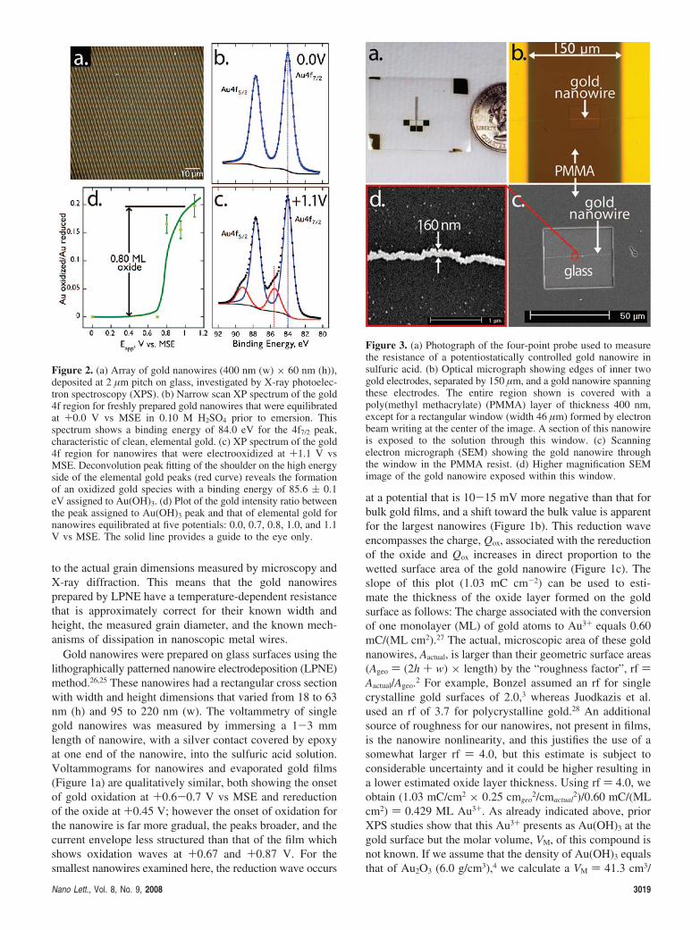
Figure 2. (a) Array of gold nanowires (400 nm (w) × 60 nm (h)),deposited at 2 µm pitch on glass, investigated by X-ray photoelec-tron spectroscopy (XPS). (b) Narrow scan XP spectrum of the gold4f region for freshly prepared gold nanowires that were equilibratedat +0.0 V vs MSE in 0.10 M H2SO4 prior to emersion. Thisspectrum shows a binding energy of 84.0 eV for the 4f7/2 peak,characteristic of clean, elemental gold. (c) XP spectrum of the gold4f region for nanowires that were electrooxidized at +1.1 V vsMSE. Deconvolution peak fitting of the shoulder on the high energyside of the elemental gold peaks (red curve) reveals the formationof an oxidized gold species with a binding energy of 85.6 ( 0.1eV assigned to Au(OH)3. (d) Plot of the gold intensity ratio betweenthe peak assigned to Au(OH)3 peak and that of elemental gold fornanowires equilibrated at five potentials: 0.0, 0.7, 0.8, 1.0, and 1.1V vs MSE. The solid line provides a guide to the eye only.
Figure 3. (a) Photograph of the four-point probe used to measurethe resistance of a potentiostatically controlled gold nanowire insulfuric acid. (b) Optical micrograph showing edges of inner twogold electrodes, separated by 150 µm, and a gold nanowire spanningthese electrodes. The entire region shown is covered with apoly(methyl methacrylate) (PMMA) layer of thickness 400 nm,except for a rectangular window (width 46 µm) formed by electronbeam writing at the center of the image. A section of this nanowireis exposed to the solution through this window. (c) Scanningelectron micrograph (SEM) showing the gold nanowire throughthe window in the PMMA resist. (d) Higher magnification SEMimage of the gold nanowire exposed within this window.
Nano Lett., Vol. 8, No. 9, 2008 3019

mol, and this translates into a layer thickness of 3.4 Å or≈0.8 ML of oxide.
To identify the oxide produced by the electrooxidation ofnanowires (e.g., Figure 1), we measured the X-ray photo-electron spectra of nanowire arrays equilibrated at appliedpotentials of 0, 0.7, 0.8, 1.0, and 1.1 V vs MSE. These arraysconsisted of thousands of linear gold nanowires 400 nm (w)× 60 nm (h) deposited using LPNE at 2 µm pitch on a glasssurface (Figure 2a). Nanowire arrays were first equilibratedat the applied potential of interest, emersed, and thenimmediately transferred to the vacuum system of the XPS.The elapsed time from electrolyte solution to ultrahighvacuum was <5 min. Narrow scan XP spectra of the Au(4f) region for wire arrays equilibrated at 0.0 V (Figure 2b)show a single Au (4f) oxidation state (spin-orbit splittingof the Au (4f) region results in a doublet with a ∆eV of3.67 eV)29 with a binding energy of 84.0 eV that is consistentwith clean, elemental gold.30 A single Au component remainsat potentials up to 0.7 V. Wires equilibrated at higherpotentials, from 0.8 to 1.1 V (Figure 2c), show, in additionto the elemental reduced Au component, a prominent
shoulder on the high energy side of the peak. This highenergy component is assigned to the formation of a Au oxidelayer. The chemical shift of this new component, fromdeconvolution peak fitting, is 85.6 ( 0.1 eV. No significantvariation in the chemical shift of this oxide component wasseen over the voltage range from 0.8 to 1.1 V. This shoulderis similar in terms of intensity and binding energy to theshoulder seen by Bonzel et al.3 for macroscopic gold sufacesequilibrated at potentials in this same range, which is to saythis chemical shift is not positive enough to be assigned toAu2O3 (4f7/2 ≈ 85.9 eV).31 Therefore the assignment of thisspecies by Bonzel3 and others28 to Au(OH)3 is consistentwith the spectra of Figure 2c. The ratio between the XPSsignal attributable to oxide and that assigned to elementalgold is plotted as a function of potential in Figure 2d. Onthe basis of the layered oxide structure model suggested byBando et al.32 and the inelastic mean free path of thephotoelectrons33 (photoelectrons collected here had an energyof 1170 eV), we estimate that approximately 0.8 monolayersof oxide, corresponding to ≈3.3 Å, is present on the goldsurface at +1.1 V vs MSE.
Figure 4. (a) Resistance, R, vs Eapp for a 40 × 145 nm gold nanowire in 0.10 M H2SO4. The change in resistance, normalized by theresistance at +0.10 V, ∆R/R0.1V, is plotted at right. The hysteresis seen in this experiment reflects the intrinsic hysteresis of the surfaceelectrochemistry, as seen for example in the cyclic voltammetry of Figure 1a. The initial and final potentials were both +0.10 V vs MSE.(b) ∆R/R0.1V vs Eapp for the oxidation of five other gold nanowires. (c) Plot of ∆R/R0.1V evaluated at +1.1 V vs MSE vs height for the sixnanowires in (a) and (b) (red trace). Also plotted are the calculated resistance change caused by the constriction in the wire diameter((∆R/Rred)dia in Table 1, green trace) and the change in p from 0.38 to 0.0 as calculated using eqs 1 and 2 ((∆R/Rred)p)0.38, blue trace) as wellas the sum of these two contributions ((∆R/Rred), black trace).
Table 1. Electrooxidation-Induced Resistance Changes for Gold Nanowires and a Comparison with TheoreticalPredictions
experimental values calculated values
wire h × w(nm × nm)
ARred
a
(kΩ)
BRox
b
(kΩ)C
∆R/Rredc
D(∆R/Rred)dia
dE
(∆R/Rp)0.38)eF
R/Rredf
GRc,eff
gHxh
Ioxide
infiltrationi
(nm)
18 × 95 36.1 42.5 0.57 0.0395 0.0807 0.12 0.8985 0.332 5.9822 × 101 24.0 27.9 0.52 0.0336 0.0661 0.10 0.8961 0.316 6.9632 × 159 5.02 5.61 0.38 0.0223 0.0477 0.071 0.8860 0.250 7.9940 × 145 5.56 6.11 0.31 0.0197 0.0414 0.062 0.8799 0.210 8.4046 × 130 5.04 5.45 0.26 0.0188 0.0382 0.058 0.8749 0.177 8.1363 × 220 1.38 1.45 0.14 0.0126 0.0284 0.041 0.8620 0.092 5.80
a Rred measured at +0.10 V vs MSE. b Rox measured at +1.10 V vs MSE. c ∆R/Rred )(Rox - Rred)/(0.31Rred) where 0.31 is the fraction of the electricallyisolated length of the nanowire that was exposed to the H2SO4 electrolyte. d (∆R/Rred)dia is calculated based upon a ∆R caused by the conversion of 0.5 nmof gold into a nonconductive gold oxide. e (∆R/Rp)0.38)dia is calculated based upon a ∆R caused by a change in p from 0.38 to 0.0 (purely diffuse surfacescattering). f (∆R/Rred)dia is the total ∆R caused both by the change in p to 0.0 and by the reduction in diameter of the nanowire by the oxide. g The effectivevalue of Rc necessary to produce the experimentally measured ∆R/Rred. h The root of the equation: Rc, eff ) (1 - x)(0.848) + x(1.0) where 0.848 isthe experimentally measured Rc for reduced gold nanowires, Rc ) 1.0 is assumed to apply at oxidized grain boundaries within the nanowire, and x is thefractional cross section of the nanowire over which grain boundaries are oxidized. i Estimate of the mean infiltration depth of the oxide into grain boundariesat the surface of the nanowire, calculated as the product of x and the wire height (nm).
3020 Nano Lett., Vol. 8, No. 9, 2008
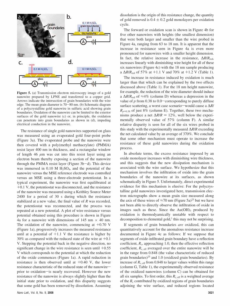
The resistance of single gold nanowires supported on glasswas measured using an evaporated gold four-point probe(Figure 3a). The evaporated probe and the nanowire werethen covered with a poly(methyl methacrylate) (PMMA)resist layer 400 nm in thickness, and a rectangular windowof length 46 µm was cut into this resist layer using anelectron beam thereby exposing a section of the nanowirethrough the PMMA resist layer (Figure 3b-d). This devicewas immersed in 0.10 M H2SO4, and the potential of thenanowire versus the MSE reference electrode was controlledversus an MSE using a three-electrode potentiostat. In atypical experiment, the nanowire was first equilibrated at+0.1 V, the potentiostat was disconnected, and the resistanceof the nanowire was measured using a Keithley Source Meter2400 for a period of 30 s during which the resistancestabilized at a new value, the final value of R was recorded,the potentiostat was reconnected, and the process wasrepeated at a new potential. A plot of wire resistance versuspotential obtained using this procedure is shown in Figure4a for a nanowire with dimensions of 145 nm × 40 nm.The oxidation of the nanowire, commencing at +0.70 V(Figure 1a), progressively increases the measured resistanceuntil at a potential of +1.1 V the resistance is higher by30% as compared with the reduced state of the wire at +0.1V. Stepping the potential back in the negative direction, nosignificant change in the wire resistance is seen until +0.55V which corresponds to the potential at which the reductionof the oxide commences (Figure 1a). A rapid reduction inresistance is then observed until at +0.40 V, the lowerresistance characteristic of the reduced state of the nanowiresprior to oxidationsis nearly recovered. However the newresistance of the nanowire is always slightly higher than theinitial state prior to oxidation, and this disparity suggeststhat some gold has been removed by dissolution. Assuming
dissolution is the origin of this resistance change, the quantityof gold removed is 0.4 ( 0.2 gold monolayers per oxidationcycle.
The forward or oxidation scan is shown in Figure 4b forfive other nanowires with heights (the smallest dimension)that were both larger and smaller than the wire probed inFigure 4a, ranging from 63 to 18 nm. It is apparent that theincrease in resistance seen in Figure 4a is even morepronounced for nanowires with a smaller height dimension.In fact, the relative increase in the resistance, ∆R/Rred,increases linearly with diminishing wire height for all of thesesix nanowires (Figure 4c) with the 18 nm sample producinga ∆R/Rred of 57% at +1.1 V and 70% at +1.2 V (Table 1).
The increase in resistance induced by oxidation is muchlarger than that which can be explained by the two effectsdiscussed above (Table 1). For the 18 nm height nanowire,for example, the reduction of the wire diameter should inducea ∆R/Rred of ≈4% (column D) whereas a depression in thevalue of p from 0.38 to 0.0scorresponding to purely diffusesurface scattering, a worst case scenarioswould cause a ∆R/Rp)0.38 of just 8% (column E). Together, these two mecha-nisms produce a net ∆R/R ) 12%, well below the experi-mentally observed value of 57% (column F). A similarrelative disparity is seen for all of the six wires probed inthis study with the experimentally measured ∆R/R exceedingthe net calculated value by an average of 370%. We concludethat some other mechanism must operate to increase theresistance of these gold nanowires during the oxidationprocess.
In absolute terms, the excess resistance imposed by anoxide monolayer increases with diminishing wire thickness,and this suggests that the new dissipation mechanism isassociated with the wire surface. We hypothesize that thismechanism involves the infiltration of oxide into the grainboundaries of the nanowire at its surfaces, as shownschematically in Figure 5. Unfortunately, direct experimentalevidence for this mechanism is elusive: For the polycrys-talline gold nanowires investigated here, transmission elec-tron micrographs show a mean grain size measured alongthe axis of these wires of ≈70 nm (Figure 5a)25 but we havenot been able to directly observe the infiltration of oxide inimages such as these. Since the Au(OH)3 produced byoxidation is thermodyamically unstable with respect todecomposition to elemental gold,1 this may not be surprising.
If segments of grain boundaries are oxidized, this canquantitatively account for the anomalous resistance increasedocumented in Figure 4c as follows: If we suppose thatsegments of oxide-infiltrated grain boundary have a reflectioncoefficient, Rc, approaching 1.0, then the effective reflectioncoefficient, Rc, eff averaged over the entire nanowire will bein the range from 0.848 (the value characteristic of reducedgrain boundaries)25 and 1.0 (oxidized grain boundaries). Byincrease of Rc, eff from 0.848 to larger values within this range(column G, Table 1), the experimentally observed resistanceof the oxidized nanowires (column C) can be obtained forall six samples. To first order, this Rc, eff is a weighted averageof the Rc contributed by oxidized regions of grain boundariesadjoining the wire surface, and reduced regions located
Figure 5. (a) Transmission electron microscopy image of a goldnanowire prepared by LPNE and transferred to a copper grid.Arrows indicate the intersection of grain boundaries with the wireedge. The mean grain diameter is 70-80 nm. (b) Schematic diagramof a polycrystalline gold nanowire in sulfuric acid showing grainboundaries. Oxidation of the nanowire can be limited to the exteriorsurfaces of the gold nanowire (c) or, in principle, the oxidationcan penetrate into grain boundaries as shown in (d), impedingelectrical conduction in the nanowire.
Nano Lett., Vol. 8, No. 9, 2008 3021

deeper within the nanowire: Rc,eff ) (1 - x)0.848 + (x)1.00where x is the fraction of the wire height into which oxidehas infiltrated, on average (column H). The depth ofpenetration of the oxide into the nanowire at its surface isthen the product of x and the wire height, tabulated in columnI of Table 1. The oxide infiltration depth calculated in thisway is uncorrelated with wire height, varying from 5.8 to8.4 nm, and this is qualitatively what would be expected forthis process, if it is occurring.
In summary, the electrical resistance of gold nanowiresmeasured in situ in dilute sulfuric acid increases in concertwith the formation of an oxide monolayer by electrooxida-tion. The magnitude of the resistance increase is as large as+70% in gold nanowires with lateral dimensions of 18 ×95 nm, much larger than can be explained by the knownmechanisms of dissipation in metals. The infiltration of oxideinto the grain boundaries at the surface of these nanowiresprovides a physically reasonable explanation for this ano-molous resistance increase, but this mechanism is notconfirmed by any direct experimental evidence.
Acknowledgment. This work was supported by theNational Science Foundation Grant CHE-0641169 (R.M.P.),the Petroleum Research Fund of the American ChemicalSociety 46815-AC 10 (R.M.P.), the DOE Office of BasicEnergy Sciences DE-FG02-96ER45576 (J.C.H.), and the UCISchool of Physical Sciences Center for Solar Energy (R.M.P.and J.C.H.). A.G.G. gratefully acknowledges economicsupport from the Department of Universities, Research andInformation Society (DURSI) of the Catalonia Governmentthrough the Grant Number 2007-BE-1-00232.
References(1) Pourbaix, M. Atlas of electrochemical equilibria in aqueous solutions,
2nd ed.; National Association of Corrosion Engineers:Houston, TX,1974.
(2) Bard, A. J.; Faulkner, L. R. Electrochemical methods: fundamentalsand applications, 2nd ed.; Wiley: New York, 2001.
(3) Peuckert, M.; Coenen, F. P.; Bonzel, H. P. Surf. Sci. 1984, 141, 515–532.
(4) Kolb, D. M.; McIntyre, J. D. Surf. Sci. 1971, 28, 321–334.
(5) Horkans, J.; Cahan, B. D.; Yeager, E. Surf. Sci. 1974, 46, 1–23.(6) Kim, Y. T.; Collins, R. W.; Vedam, K. Surf. Sci. 1990, 233, 341–
350.(7) Chopra, K. L.; Randlett, M. R. J. Appl. Phys. 1967, 38, 3144–3147.(8) Lucas, M. S. P. Thin Solid Films 1971, 7, 435–444.(9) Campbell, D.; Morley, A. Rep. Prog. Phys. 1971, 34, 283–368.
(10) Ogawa, S. J. Vac. Sci. Technol. 1978, 15, 363–365.(11) Marsocci, V. A.; Shue, S. S. J. Appl. Phys. 1971, 42, 5047–5050.(12) Dayal, D.; Wissman, P. Thin Solid Films 1977, 44, 185–191.(13) Schumacher, D.; D., S. Surf. Sci. 1982, 123, 384–396.(14) Chauvineau, J. P.; Marliere, C. Thin Solid Films 1985, 125, 25–31.(15) Dayal, D.; Wissman, P. Vak.-Tech. 1989, 38, 121–133.(16) Steinlesberger, G.; Engelhardt, M.; Schindler, G.; Steinhogl, W.; von
Glasow, A.; Mosig, K.; Bertagnolli, E. Microelectron. Eng. 2002, 64,409–416.
(17) Steinhogl, W.; Schindler, G.; Steinlesberger, G.; Engelhardt, M. Phys.ReV. B 2002, 66, 075414.
(18) Schindler, G.; Steinlesberger, G.; Engelhardt, M.; Steinhogl, W. Solid-State Electron. 2003, 47, 1233–1236.
(19) Steinhogl, W.; Schindler, G.; Steinlesberger, G.; Traving, M.; Engel-hardt, M. J. Appl. Phys. 2005, 97, 023706.
(20) Steinhogl, W.; Steinlesberger, G.; Perrin, M.; Scheinbacher, G.;Schindler, G.; Traving, M.; Engelhardt, M. Microelectron. Eng. 2005,82, 266–272.
(21) Fuchs, K. Proc. Cambridge Philos. Soc. 1938, 34, 100–108.(22) Sondheimer, E. H. AdV. Phys. 1952, 1, 1–42.(23) Mayadas, A. F.; Shatzkes, M. Phys. ReV. B 1970, 1, 1382–1389.(24) Devries, J. W. C. Thin Solid Films 1988, 167, 25–32.(25) Xiang, C.; Kung, S. C.; Taggart, D.; Yang, F.; Thompson, M. A.;
Guell, A. G.; Yang, Y.; Penner, R. M. ACS Nano 2008, 10.1021/nn800394k.
(26) Menke, E. J.; Thompson, M. A.; Xiang, C.; Yang, L. C.; Penner, R. M.Nat. Mater. 2006, 5, 914–919.
(27) Angersteinkozlowska, H.; Conway, B. E.; Hamelin, A.; Stoicoviciu,L. Electrochim. Acta 1986, 31, 1051–1061.
(28) Juodkazis, K.; Juodkazyte, J.; Jasulaitiene, V.; Lukinskas, A.; Sebeka,B. Electrochem. Commun. 2000, 2, 503–507.
(29) Moulder, J. F. Handbook of x-ray photoelectron spectroscopy: areference book of standard spectra for identification; PhysicalElectronics: Eden Prairie, MN, 1995.
(30) Seah, M. P.; Smith, G. C.; Anthony, M. T. Surf. Interface Anal. 1990,15, 293–308.
(31) Pireaux, J. J.; Liehr, M.; Thirty, P. A.; Delrue, J. P.; Caudano, R.Surf. Sci. 1984, 141, 221–232.
(32) Bando, H.; Koizumi, K.; Oikawa, Y.; Daikohara, K.; Kulbachinskii,V.; Ozaki, H. J. Phys.: Condens. Matter 2000, 12, 5607–5616.
(33) Powell, C. J.; Jablonski, A. NIST Electron Inelastic-Mean-Free-PathDatabase, Version 1.1 ed.; National Institute of Standards andTechnology: Gaithersburg, MD, 2000.
NL8021175
3022 Nano Lett., Vol. 8, No. 9, 2008