Embed Size (px)
Citation preview
Portland State University Portland State University
PDXScholar PDXScholar
Dissertations and Theses Dissertations and Theses
1993
Correction of Chromatic Aberration with an Electron Correction of Chromatic Aberration with an Electron
Mirror Mirror
Michael Stewart Mauck Portland State University
Follow this and additional works at: https://pdxscholar.library.pdx.edu/open_access_etds
Let us know how access to this document benefits you.
Recommended Citation Recommended Citation Mauck, Michael Stewart, "Correction of Chromatic Aberration with an Electron Mirror" (1993). Dissertations and Theses. Paper 1171. https://doi.org/10.15760/etd.1170
This Dissertation is brought to you for free and open access. It has been accepted for inclusion in Dissertations and Theses by an authorized administrator of PDXScholar. Please contact us if we can make this document more accessible: [email protected].
CORRECTIONOFCHROMATICABERRATION
WITH AN ELECTRON MIRROR
by
MICHAEL STEWART MAUCK
A dissertation submitted in partial fulfillment of therequirements for the degree of
DOCTOR OF PHILOSOPHYIn
ENVIRONMENTAL SCIENCES AND RESOURCES:PHYSICS
Portland State University1993
TO THE OFFICE OF GRADUATE STUDIES:
The members of the Committee approve the dissertation of
Michael Stewart Mauck presented December 1, 1992.
Gertrude Rempfer, Chair i
Erik ao야뿜ffiU
Laird C. Brodi
APPROVED:
John(요 Rueter, Direct얀’ Environmental Sciences and Resources Program
Roy
AN ABSTRACI’ OF THE DISSERTATION OF Michael Stewart Mauck for the
Doctor of Philosophy in Environmental Sciences and Resources: Physics
presented December 1, 1992.
Title: Correction of Chromatic Aberration with an Electron Mirror.
APPROVED BY THE MEMBERS OF THE DISSERTATION COMMITTEE:
Erik Bod명야I 니
Robert \T. 0 ’Brien
Oiloff
2
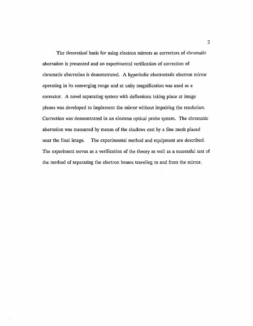
The theoretical basis for using electron mirrors as correctors of chromatic
aberration is presented and an experimental verification of correction of
chromatic aberration is demonstrated. A hyperbolic electrostatic electron mirror
operating in its converging range and at unity magnification was used as a
corrector. A novel separating system with deflections taking place at image
planes was developed to implement the mirror without impairing the resolution.
Correction was demonstrated in an electron optical probe system. The chromatic
aberration was measured by means of the shadows cast by a fine mesh placed
near the final image. The experimental method and equipment are described.
The experiment serves as a verification of the theory as well as a successful test of
the method of separating the electron beams traveling to and from the mirror.
ACKNOWLEDGMENTS
The author is deeply indebted to Dr. Gertrude Rempfer for her untiring
interest in her students and her work. Her genius has been a constant source of
inspiration for this work as well as a lifetime of research possibilities. Many
others contributed to the accomplishment of this project. Dr. O. Hayes Griffith at
U. of O. and his capable staff provided the PEM application background as well
as administrative and financial assistance. I tha퍼<: Polly Habliston for the prompt
German literature references. Rudy Zupan and the late Garo Arakelyan of the
Science Support Shop at PSU were responsible for the precision machining of the
many electron optical elements needed in these experiments. Walter Skoczylas
and Denis Desloge were of invaluable assistance in preparing the text and figures.
만le financial assistance of the M. J. Murdock Charitable Trust and gifts from my
Mother made this dissertation possible. For the contents of Chapter III, the
authors thank Dr. O.H. Griffith for valuable discussions, W.P. Skoczylas and D.M.
Desloge for expert engineering and technical support, and David Ryan for
photographic services. Financial support from the National Science Foundation
(Grant No. DIR8907619) is gratefully acknowledged.
ACKNOWLEDGMENTS
TABLE OF CONTENTS
PAGE
11l
LIST OF TABLES . . . . . . . . . . . . . . . . . . . . . . . . . . . . . . . . . . . . . . . . . . . . vi
LIST OF FIGURES vii
CHAPTER
I BACKGROUND 1
Introduction 1
Historical 4
Light OpticsElectron Optics
II THEORETICAL. . . . . . . . . . . . . . . . . . . . . . . . . . . . . . . . . .. 13
Introduction 13
The Electric Field Equations . . . . . . . . . . . . . . . . . . . .. 13
The Hyperbolic Electron Mirror 19
Calculation of the Properties of theHyperbolic Electron Mirror forSymmetric Rays
Electron Trajectories in the Hyperbolic FieldDeflection by the Aperture LensThe Paraxial Object/Image Distance and the
Spherical and Chromatic AberrationCoefficients of the Mirror
v
III CORRECflON OF CHROMATIC ABERRATIONWITH AN ELEcrRON MIRROR 31
Introduction 31
The Electron Optical System . . . . . . . . . . . . . . . . . . . .. 32
Method of Determining Aberrations 34
Apparatus . . . . . . . . . . . . . . . . . . . . . . . . . . . . . . . . . .. 37
Results and Discussion 41
IV SIGNIFICANCE OF RESULTS 47
Transmission Electron Microscope 49
Emission Microscope 51
Electron or Ion Probe . . . . . . . . . . . . . . . . . . . . . . . . .. 52
Conclusion ; 54
REFERENCES.............................................. 56
APPENDICES
A THE BEAM-SEPARATING SYSTEM 59
B DETAILS OF THE EXPERIMENT 65
TABLE
II
LIST OF TABLES
PAGE
Mirror and Lenses 46
Projection Lens Properties 71
LIST OF FIGURES
PAGE
Construction of elemental volume element
for obtaining divergence of electric
field . . . . . . . . . . . . . . . . . . . . . . . . . . . . . . . . .. 15
2. Equipotential surfaces for the rotationally
symmetric hyperbolic field 20
3. Theoretical model of the hyperbolic mirror 21
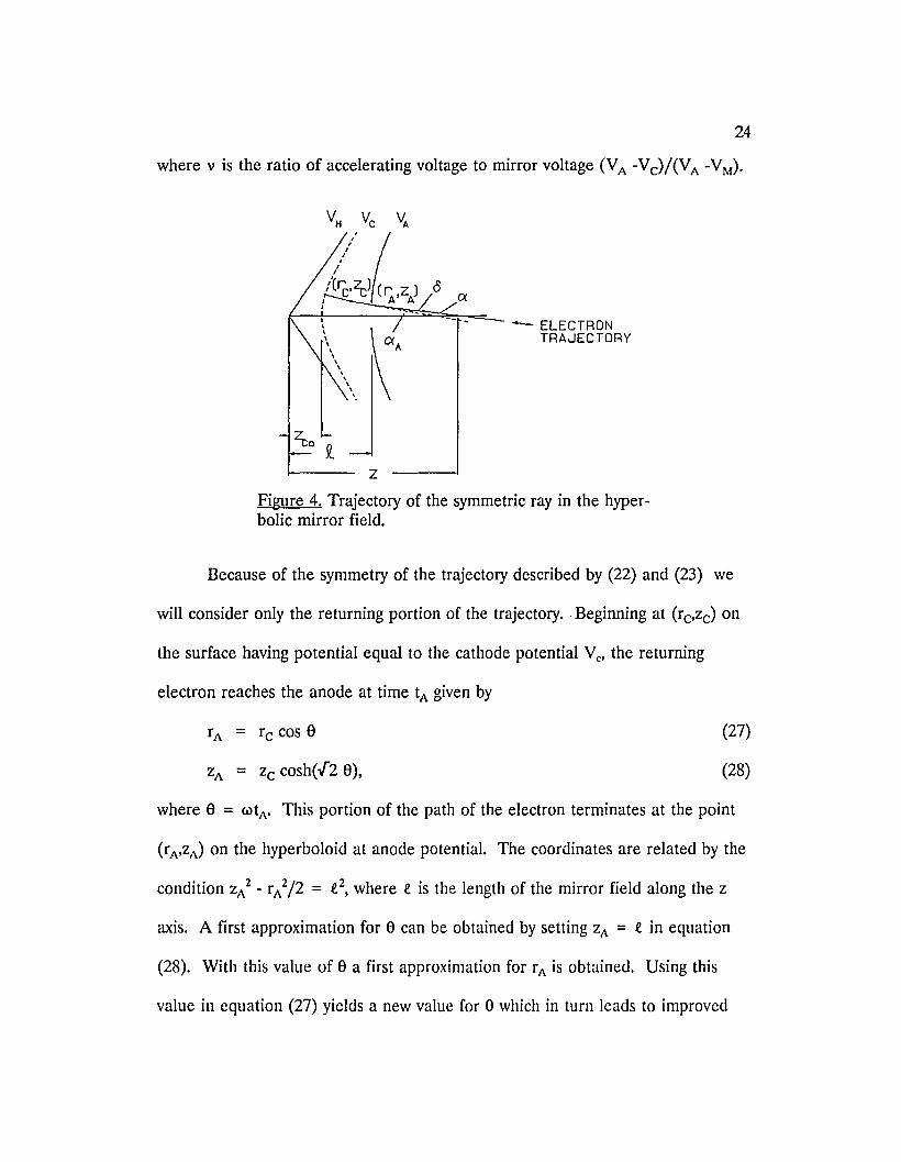
4. Trajectory of the symmetric ray in the
hyperbolic mirror field 24
5. Theoretical (a) paraxial object/image
distance and (b) aberrations as a
function of the voltage ratio for the
hyperbolic electron mirror in the
symmetric mode 28
6. The electron optical arrangement used for the
experimental study of aberration correction
by an electron mirror 33
FIGURE
1.
Vlll
7. Diagram illustrating the relation between
the magnification of the shadow cast by
the mesh and the location of the image
formed by the objective lens . . . . . . . . .. 35
8. Photograph of the aberration-correction
experiment set-up in the electron
optical bench 39
9. A scale drawing of the hyperbolic mirror used
in the experiments 40
10. A scale drawing of the objective lens used in the
aberration-correction experiments . . . . . . . . . . .. 41
11. Shadow patterns indicating several stages of chromatic
aberration correction: (a) undercorrection,
(b) correction, (c) overcorrection 42
12. Shadow pattern obtained under conditions similar
to those for Figure 11, but without the
correcting system 45
13. Separation of incident and returning beams by a
magnetic field 61
14. Schematic of power supplies for experimental study. . .. 68
CHAPTERI
BACKGROUND
INTRODUCTION
The objective of this work is the development of a method of correcting
chromatic aberration in an electron optical system by means of a hyperbolic
electrostatic electron mirror. 까le research reported in this dissertation
demonstrates the first experimental verification of the theory of aberration
correction with mirrors. 까lis achievement provides the basis for extending the
resolution limit of electron microscopes and should result in new and important
discoveries in all branches of science.
In light optics, chromatic aberration manifests itself as a change in lens
power and image position as a function of the wavelength or color used to form
the image. We are all familiar with the phenomenon of color dispersion from the
occurrences of the rainbow or the colored cusp formed in light passing through a
glass of water and falling on the table. In these every day examples of dispersion,
light of differing colors is refracted by differing amounts. In the case of lenses,
the dispersion of light results in concentric circles of color being formed around
each image point, blurring the image and limiting the resolution of the image.
2
The invention of the achromat has permitted the correction of this primary defect
in light optics.
In electron optics a difference in the velocities of electrons passing through
an electron lens causes an analogous behavior. 까lis velocity aberration is also
referred to 잃 chromatic aberration in analogy with light optics. Here our every
day experience is limited, but aberration of electron beams, for example, sets the
upper limit to the brightness in projection television tubes. In electron optics,
unlike light optics, there is no rotationally symmetric lens element having the
opposite sign of chromatic aberration. However, an electron mirror does have
chromatic aberration of opposite SigH from that of electron lenses. By
incorporating a mirror in a lens system to compensate the lens aberrations, the
entire system can be made free, to first order, from chromatic aberration.
Work on mirrors has been hindered in the past by the need for a practical
means of separating the beams headed toward and away from the mirror. The
first scheme proposed for incorporating a mirror as a correcting element required
the beam to pass through the object twice, compromising the intended benefits.
In the work reported here an efficient optical arrangement for incorporating a
mirror element in an optical system is demonstrated and confirms the mirror’s
potential as a correcting element in a variety of electron optical devices.
Demonstration of the correction of chromatic aberration in electron optics
provides the basis for improved resolution and larger beam currents in electron
and ion optical devices. Correction of chromatic aberration is of particular
3
interest in the case of probe-forming instruments, especially focused ion beam
instruments, where the energy spread is large [1], and also in emission electron
microscopes and related low-energy electron microscopes, where the accelerating
field has a large chromatic aberration coefficient [2,3].
Aberration correction would be especially beneficial to the photoelectron
microscope (PEM) where direct imaging of the DNA molecule lies near the
resolution limit of this instrument [2]. In the photoelectron microscope,
photoelectrons are emitted from the specimen by exposure to ultraviolet light.
’The photoelectrons are accelerated and focussed into a magnified image of the
object. The relatively gentle action of the ultraviolet light in the PEM compared
to direct electron bombardment of the specimen in the TEM results in less
damage to the objects under study. ’The combination of photoelectric yield and
topographic contrast, with the surface specific nature of image formation in the
PEM is advantageous for biological imaging. Improving the resolution from the
present limit of about 100 A to 20 A or less would enable direct imaging of an
important new range of biological structures in the PEM.
Ion beam spectrometers and probe type instruments could also incorporate
this chromatic correction to increase resolution and sensitivity to minute
environmental contaminants. Increasing need to extend the limits of detection in
analytical instruments will stimulate the design of new improved instruments
incorporating the electron mirror. Furthermore, the microelectronics industry is
constantly moving toward producing integrated circuits with smaller features.
4
Presently the lithography industry is reaching the resolution limit of light optics
and is investigating the possibility of utilizing x-rays to reach smaller sizes.
Increased resolution in electron and ion optics provides an alternative to the use
of x-rays for production and analysis of smaller geometries. Another entirely new
branch of micro-machining fabrication called "nanotechnology" has developed
around lithography and micro-machining utilizing ion probes. Both resolution and
throughput of ion beam probes are limited by electron lens aberrations.
Correction of chromatic and/or spherical errors with the electron mirror will
revolutionize this field. These are a few of the anticipated benefits from the
correction of the primary defects in electron optics. The demonstration of the
correction of chromatic aberration described in this work is a significant step in
realizing these objectives.
HISTORICAL
Light Ootics
Correction of chromatic aberration in light optics was accomplished over
two hundred years ago. Spurred on by the mistaken belief that the eye is
achromatic Chester Moor Hall is credited [4] with constructing the first
achromatic telescope in about 1733. Later, John Dolland patented a practical
achromat in 1758 [5]. The achromat corrects both chromatic and spherical
aberration. The achromat enabled larger telescope lenses to be made, spawning
the modern age of astronomy. It is difficult to imagine our world today without
5
microscopes, cameras, camcorders, copiers, microfilm, and the host of
manufacturing processes that depend upon the achromat.
When aberrations have been corrected, the ultimate resolution limit
depends upon the diffraction limit due to the wave nature of light. The
diffraction limit rd is given by
rd = 0.61 A / ( n sin ex )
where λ is the wave length of light, n is the index of refraction around the
specimen, and ex is the maximum angle of light accepted by the optics. The
resolution limit is about 3000 A for visible light.
n//‘,‘、
Electron Ootics
The ultimate limit to resolution in electron optics is also set by the wave
nature of electrons to
다 = 0.61 λ / sin ex (2)
where the wavelength in Angstroms is given by λ =J( 150 / V ) and V is the
electron accelerating v이tage in volts. The wavelength is 0.05 A. for electrons
accelerated through 60 kV. The angle ex accepted by the lens system for a 60 kV
beam is usually quite small, ... 0.01 rad. resulting in a resolution limit of 3 A. The
small angle is a consequence of a compromise between the diffraction error,
which increases as the angle decreases, and the lens aberration error which
increases as the angle increases. In this case we see that the 3 A. resolution limit
is nowhere near the 0.05 A wavelength of the electrons. The case for ions with
6
their shorter wavelengths corresponding to their greater mass is even more
disparate. The potential gains in resolution in electron and ion beams by the
correction of aberrations is large and many have undertaken to accomplish this
goal.
The earliest work published on electron mirrors was done by Henneberg
and Recknagel [6], Recknagel [7], and Hottenroth [8]. πle discovery that
mirrors had the opposite sign of chromatic aberration from lenses was apparently
Henneberg’s as he applied for a patent in May 1935 in Germany and was
subsequently granted a U.S. patent [9] in 1939. The book by Zworkin et aI. [1이,
published in 1947, also demonstrated conclusively that even the flat electrostatic
mirror was overcorrected for both spherical and chromatic aberrations.
In Scherzer’s celebrated paper [11] of 1936, he proved that the chromatic
and spherical errors of conventional electron lenses were always of the same sign.
Efforts to reduce aberrations had, by this time, resulted in the growing concern
that the enormous resolution potential of electron microscopy could be only
partially realized.
In another paper [12] Scherzer delineated the possible ways of overcoming
aberrations in electron lenses. The list contains the various conditions under
which corrections are theoretically possible in a rotationally symmetric electron
lens system. Each of these methods involves some kind of intrusion into the
space in which the electron beam would normally travel in an uncorrecte이 system.
In principle spherical aberration can be corrected by the use of multipole electric
7
or magnetic fields. The muItipole fields are used to remove the rotational
symmetry of an electron optical system. It is then necessary to restore the
rotational symmetry after correction of spherical aberration [13,14]. Both
spherical and chromatic aberrations can, in principle, be corrected by combining
electric and magnetic poles in the corrector [15]. Another approach is to
construct a diverging correcting element. This can be done by utilizing a
conducting foil window which is nearly transparent to electrons on one or more
electrodes of an electrostatic lens. Here the diverging component is combined
with an undercorrected converging lens to form a spherically corrected converging
doublet [16,17] which can be partially corrected for chromatic aberration. In
principle the field in a lens can also be modified by a space charge injected along
the axis of the lens. Time-varying focusing fields and pulsed electron beams can
also, in principle, be used to produce lenses corrected for aberrations. Recent
reviews of such approaches to the correction of chromatic and spherical
aberrations are found in Refs. [18] and [19]. The mirror is the only rotationally
symmetrical geometry in Scherzer’s list which doesn’t require the beam to traverse
some physical obstacle or the electric or magnetic field to vary in time. These
restrictions are important in preserving the potential of the optical system to
produce resolution of atomic dimensions.
The history of the mirror was known to Ramberg, and the publication of
the list of possibilities for overcoming aberrations articulated by Scherzer may be
what led Ramberg to investigate the possibility of utilizing a mirror to improve
8
the resolution of the electron microscope. In 1948 Ramberg [20] proved that the
mirror field he studied analytically would have overcorrected chromatic
aberration, that is, higher energy electrons would focus closer to the mirror rather
than farther away as in the usual case with lenses. In his scheme, the specimen
was situated between the objective lens and the mirror. The illuminating beam
would have to pass through the specimen on the way to the mirror and again on
the way back to the objective. πle mirror was used in the symmetrical mode with
the magnification near unity. In this case the aberration of the mirror would have
to be numerically equal to that of the objective, and the mirror and objective
would have to have external focal points. 까le impracticality of having the beam
pass through the specimen a second time as well as the restrictive optical
constraints caused Ramberg to conclude that "the correction of electron
microscope objectives by electron mirrors, employed in the manner described,
meets serious practical difficulties." After Ramberg’s statement of the
impracticability of using a converging mirror to correct the aberrations of lens
systems was published, further work using mirrors for this purpose was not seen
for two decades.
However, mirrors were interesting for reasons other than for aberration
correction. For example, the development of a commercial energy analyzing
electron microscope by Zeiss utilized a mirror as part of the energy filter. An
electron mirror utilizing a plane mirror electrode was incorporated into a
9
magnetic prism-mirror-prism geometry by Castaing and Henry [21] in 1962 as an
element of the high resolution energy filter in this design.
In 1973 Henkelman and Ottensmeyer [22] were investigating a concave
mirror geometry for a use similar to the Castaing filter, and made this remark in
closing: ’'The demonstration by Ramberg (1948) that the dimensions of a
correcting mirror must be unobtainably small does not apply for images which
have been further magnified as in this case. Whether such a correction can be
realized practically has not yet been investigated." Although they did not have
aberration correction in view in their work, the use of a mirror in their geometry
with the image of the specimen at other than unity magnification eliminated one
of the objections to the practical realization of the mirror for aberration
correction. Mirrors were considered in similar applications by Lichte and
Mollenstedt [23] in 1979. It was, in fact, the mirror’s potential of large chromatic
aberration that was found of interest as a dispersing element in the energy
analyzer studied by van der Merwe [24] in 1981.
In my Master’s thesis [25] in 1969 both the theoretical and experimental
properties of the hyperbolic electrostatic electron mirror were studied. The only
previous mention of the hyperbolic field model in the literature is in the limiting
case of an analytical model by Lafferty [26] in 1947. In this case only the first
order properties were investigated. The hyperbolic field is a partic비arly
instructive system to study since the equations for the radial and axial motion are
separable and have analytic solutions. By taking into account the terminating
10
aperture lens effect, the theoretical model closely mimics the real mirror and
much insight into the behavior of the mirror properties can be understood by
studying the theory. This work confirmed the expectation that the converging
hyperbolic field possessed aberrations suitable for correction of electron lens
systems. No separation scheme was required in my experimental investigation.
The mirror was used at a magnification different from unity, and the 0비ect and
image were at different locations so that the incident and returning beams
traveled along different paths. A hole cut in the photographic film used to record
the reflected beam permitted the incident beam to reach the mirror while the
returning beam was intercepted by the film surrounding the hole. The properties
of the mirror could be studied in this way but this scheme would be impractical
for a microscope.
The need to separate the incident beam from the reflected beam without
impairment of resolution by aberrations of the deflection system remained as an
obstacle until the present work. Work toward realizing a practical separation
scheme began in the allied field of mirror microscopy. Here, the specimen itself
is the mirror, and is the 。이ect to be imaged. The incident beam is separated
from the reflected beam by a magnetic turning field. The earliest use the
magnetic separator is found in the paper by Hottonroth [8] where the mirror is
first investigated experimentally. Distortion and aberrations of the turning field
used in this way preclude it from use in high resolution aberration correction.
Subsequent searching for the lowest aberration magnetic turning fields exhausted
11
the potential of bringing these aberrations to a sufficiently low magnitude to use
at high resolution. The situation with the separation system was not unlike the
quest for the lens with the highest resolution for electron microscopy. No
theoretical limit was known for the minimum aberration possible and so the
search went on for the best geometry until the possibilities were exhausted.
In order to utilize the aberration correction properties of a mirror, a
practical method of separating the incident and reflected beams must be
employed. One method of separation that had not been tried is to separate the
beams in an image plane. For this case, the object and image must both be
superimposed in a separating magnetic turning field. This stipulation requires the
mirror to operate in its symmetrical mode with equal object and image distances.
The experimental investigation of the mirror’s properties in the symmetric mode,
in turn, requires the use of the same beam separation scheme where the
deflections take place at image planes.
In the present study the equations governing the motion of electrons in the
hyperbolic electric field in its symmetric mode are reviewed in Chapter II. Here
the theoretical properties are presented utilizing an analytic model for the
hyperbolic electron mirror previously published by Dr. Rempfer and myself [27]
and Rempfer [28]. In this study a practical high resolution beam separation
scheme is developed and used to demonstrate correction of chromatic aberration
in a system of lenses by the mirror in Chapter III. The experimental properties of
the mirror are deduced from the res비ts of the aberration correction of the system
12
and compared with the results of the theoretical study of the mirror properties.
Satisfactory correlation between the mirror’s theoretical and experimental
properties are found. In Chapter IV the significance of the research is discussed
and applications where the correction of chromatic aberration would be expected
to be beneficial are suggested. The techniques developed to accomplish the beam
separation and correction are presented in detail in Appendix A. The separation
system developed here has utility beyond aberration correction and has become
the subject of further development of the low energy reflection electron
microscope [29] and will be useful in other electron and ion instruments. The
details of the experimental procedure and equipment are described in Appendix
B. Further evidence for the practicality of the lens-mirror achromat found in this
study is discussed.
CHAPTER II
THEORETICAL
INTRODUCTION
To begin I will review the theoretical background leading to the electron
optical properties of the hyperbolic electron mirror. This review will include: the
equations necessary to describe the motion of electrons in electric fields; the steps
leading to the equations for the potential distribution in rotationally symmetric
electric fields satis덴ng Laplace’s equation, of which the hyperbolic field is a
special case; the solution of the electron trajectories in the hyperbolic field and
the electron optical properties of the hyperbolic electron mirror.
THE ELECTRIC FIELD EQUATIONS
Here we begin from first principles and deduce the equations governing
the electrostatic electric field and the motion of electrons in such a field. The
essential physical law to begin with is Coulomb’s force law
F = k q q’/ r2 (3)
where F is the force between two "point" charges q and q’ a distance r apar t.
The electric field E produced by a charge q is defined to be the limit of the
14
ratio of the force F on a test charge q' (introduced at the point of interest) to the
quantity of charge on the test charge as the magnitude of the test charge
approaches zero.
E = limq’에 (F/q’ ) (4)
In this formalism a charge is said to produce an electric field extending to infinity
in all directions in proportion to the magnitude of the charge, inversely
proportional to the square of the distance from a point charge and dependent
upon the electric properties of the intervening space. The introduction of the
concept of the field is of great use in that vector algebra and vector calculus can
be brought to bear on the mathematical solutions of practical problems.
A field can be represented by lines of force where the direction of the field
is represented by the direction of the lines, and the strength of the field by the
number of lines per unit area at right angles to the direction of the field. Because
of the inverse square law these lines of force are continuous in charge-free space.
The same property holds in free space for the field lines due to a distribution of
charge. For a given volume in empty space the number of lines entering is equal
to the number leaving the volume by Gauss’s law. This can be expressed by
div E = O. (5)
까le divergence of a vector is the net excess of lines per unit volume leaving an
infinitesimal region. The calculation of the divergence of the electric field is
illustrated for Cartesian coordinates in Figure 1. The net flux through the two
faces normal to the x-axis is
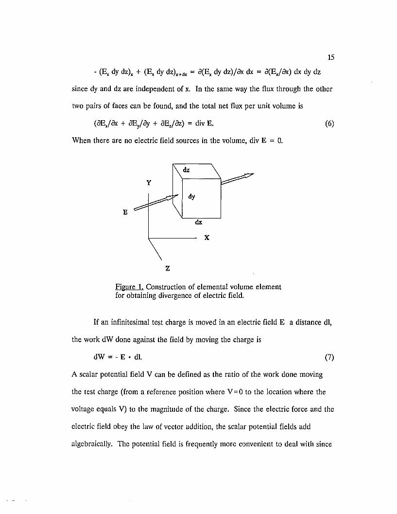
15
- (Ex dy dz)x + (Ex dy dZ)x+dx = a(Ex dy dz)jax. dx = a(Exjax.) dx dy dz
since dy and dz are independent of x. In the same way the flux through the other
two pairs of faces can be found, and the total net flux per unit volume is
(aExlax. + aEy/iJy + aEz/&) = div E.
When there are no electric field sources in the volume, div E = O.
(6)
E
z
Fi웰I흐h Construction of elemental volume elementfor obtaining divergence of electric field.
If an infinitesimal test charge is moved in an electric field E a distance dl,
the work dW done against the field by moving the charge is
dW = - E • dl.
A scalar potential field V can be defined as the ratio of the work done moving
(7)
the test charge (from a reference position where V = 0 to the location where the
voltage equals V) to the magnitude of the charge. Since the electric force and the
electric field obey the law of vector addition, the scalar potential fields add
algebraically. The potential field is frequently more convenient to deal with since
16
it is a scalar and more easily calculated. The electric field is related to the scalar
potential V by
E = - grad V (8)
The gradient of a scalar is the change in the value of the scalar per unit
distance normal to a surface of constant value (i. e., the limit as the distance goes
to zero). The gradient of V is the rate of change of potential with distance in the
direction normal to the surface at potential V. In Cartesian coordinates
grad V = i avIax + j avI매 + k avlaz (often written V V)
That grad V is normal to the surface = constant can be seen by moving a point a
differential amount on an equipotential surface, so that
dV = (aVlax) dx + (aVlOy) dy + (aVlaz) dz = 0
Since the vector i dx + j dy + k dz can take any orientation on the surface, the
vector i avIax + j avIoy + k avIaz must be normal to the surface because the
cosine of the angle between the two vectors is zero. Since E = - grad V,
div E = div (grad V) = 0 (often written V2 V = 이. (9)
This is Laplace’s equation which tells how the potential function, and hence the
electric field, varies in free space for given boundary conditions. In Cartesian
coordinates the Laplacian becomes
V2 V =앤v/ax2 + 훈VI이,z + 앤v/az2 = 0m/
l,‘、
In other coordinate systems the distances corresponding to increments of
the coordinates are not necessarily equal to the change in coordinates. Since the
hyperb이ic mirror field is rotationally symmetric about the optical 없is it is
17
convenient to express the Laplacian in terms of the cylindrical coordinates rand
z. To do this both div and grad need to be expressed in the cylindrical coordinate
system. Expressing the distance increments as dS1 = hI dql' etc., grad V is
e1 av/as1+ e2 av/as2+ e3 av/<3'33 =
e1(1/h1) av/aql + e2(1/h2) av/aqz + eil/h3) av/a~ = - E,
where the e-vectors are unit vectors in the direction of the increasing coordinates.
Similarly, the divergence of E is
[a/as1(E1 ds2ds3)ds1 + a/as2(Ez ds3ds1)ds2
+ a/asiE3ds1ds2)ds3] / (ds1ds2ds3) =
- {a/aql[(h2h3/h1)aV/aql] + a/aqz[(h3h1/h2)aV/aqz]
+ a/a~[(hlh2/h3)aV/a~]} / (h1h2h3).
For cylindrical coordinates r, φ, z
dS1 = dr, dS2 = r dφ, and dS3 = dz,
and Laplace’s equation is
azvfar + (l/r)aVfar + (1/r)앤v/a</} + 하v/az2 = 0.m/
tl
、
Since the electric field has rotational symmetry the term involving φ drops
out, leaving
훈Vfar + (l/r)aVfar + 앤v/az2 = 0. (12)
If we assume for V(r,z) a Taylor expansion in powers of r from the 없is
outward
V(r,z) = V(O,z) + r(aV/ar)o + (r/2!)(하V/ar2)。
+ (~/3!)(허v/a~)o + .. , (13)
(14)
18
The requirement that this expression have axial symmetry leads to the following
conditions: the odd derivatives with respect to r are zero since VCr) must equal
V(-r); the even derivatives of V with respect to r are related to the derivatives
with respect to z on the 없is, thus
(앙Vj iJ'?)o = - vz V(O,z)"
(Cf +2Vjarn+2)o = - (n+l)j(n+2) (CfVjarn)o"
where the primes refer to derivatives with respect to z. When these conditions
are used to eliminate the partial derivatives with respect to r, the power series
expression for V above becomes
V(r,z) = V(O,z) - (~j22)V(O,Z)" + (r4j2242)V(O,z)""
+ (r6j224262)V(O,z)(6) + ...
and the electric field is
- E = V V = er avjar + e~ avjaifl + 윌 aVjaz.
까Ie radial component of the electric field is
Er = - av jar = vz V"(O,z)r + higher order terms. (15)
From this equation we see that to first order the radial electric field Er is
proportional to the distance r offaxis.
The radial electric field exerts a radial force F = - e Er on the electron,
and from Newton’s 2nd law
Fr = m r = - e Er = - liz e V"(O,z) r + . (16)
The deflections of the electron trajectories are therefore also proportional to first
order to the height off 따is. Thus, every rotationally symmetric electric field is a
19
focusing field for electrons, unless V"(O,z) = 0, in which case V is either constant,
or has a uniform gradient.
THE HYPERBOLIC ELECfRON MIRROR
The hyperbolic electron mirror is based on the rotationally symmetric
hyperb이ic potential field as developed in the pre띠ous section. From (14) the
potential field having cylindrical symmetry and satis다ring Laplace’s equation can
be expressed to first order as
V(r,z) = V(O,z) - V"(0,z)r/22 + higher order terms (17)
where again, rand z are radial and axial cylindrical coordinates. When the third
and higher order derivatives are zero in the field described by (17), and when
V"(O,z) = a constant ¢ 0, we are left with the hyperbolic potential field. The
integration of V" (O,z) with respect to z yields V(O,z) = C1z2/2 + ~z + ~. ’The
origin can be chosen so that the equation for the hyperbolic field becomes
V(r,z) - Vo = C1z2/2 - C1r/22 = k(Z2- 년/2), (18)
where the potential at the origin is Vo'
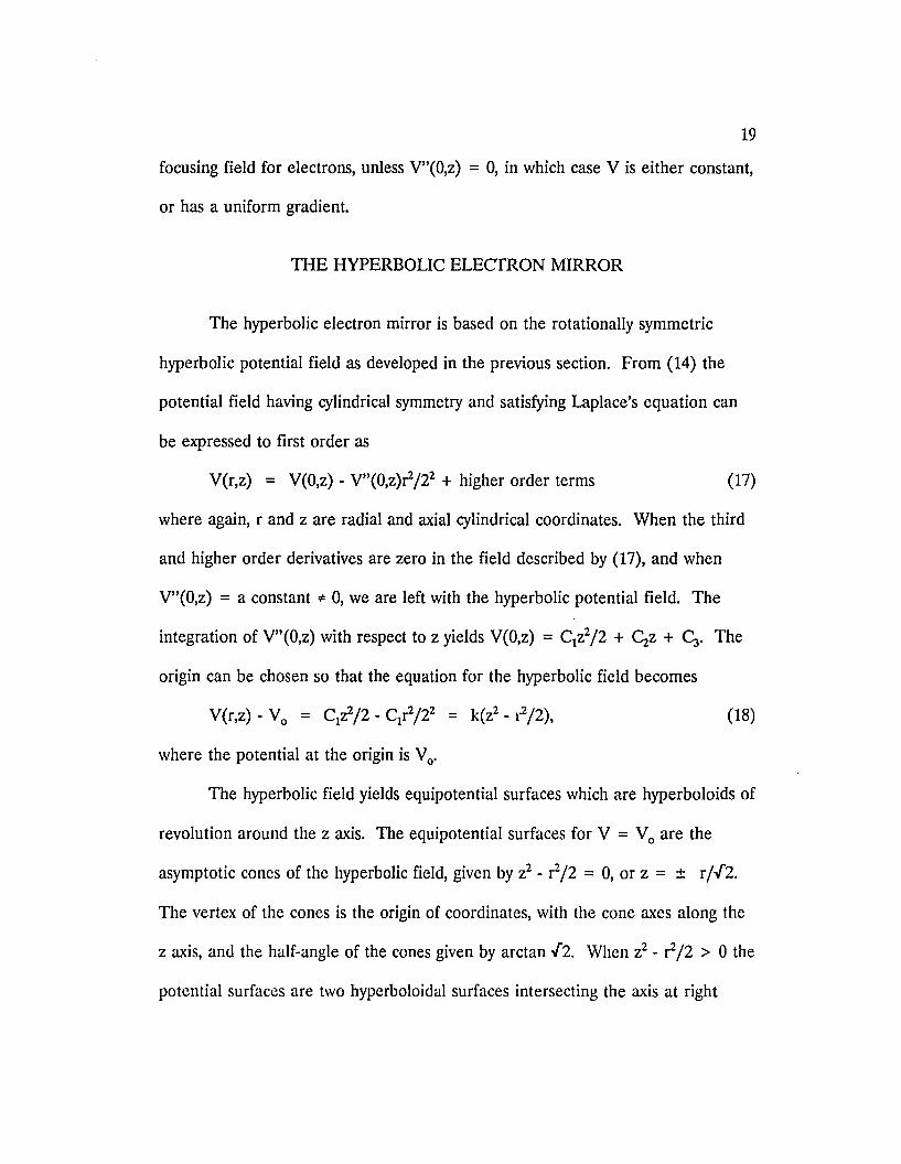
The hyperbolic field yields equipotential surfaces which are hyperboloids of
revolution around the z axis. The equipotential surfaces for V = V0 are the
asymptotic cones of the hyperbolic field, given by Z2 - r /2 = 0, or z = ± r/..[2.
The vertex of the cones is the origin of coordinates, with the cone axes along the
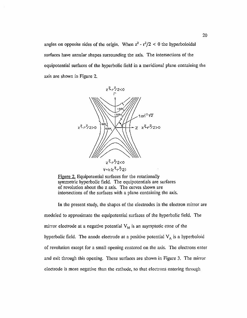
z axis, and the half-angle of the cones given by arctan ..[2. When Z2 - r /2 > °the
potential surfaces are two hyperboloidal surfaces intersecting the axis at right
20
angles on opposite sides of the origin. When Z2 - r /2 < 0 the hyperboloidal
surfaces have annular shapes surrounding the axis. The intersections of the
equipotential surfaces of the hyperbolic field in a meridional plane containing the
axis are shown in Figure 2.
2 2z-=-rI'2<0
「
2 2z-=-rI'2>0 2 2Z z-=-rI'2>0
z 르 r‘주 2<0
V=k (z르「용2)
Fi뀔!!효으‘ Equipotential surfaces for the rotationallysymmetric hyperbolic field. The equipotentials are surfacesof revolution about the z axis. The curves shown areintersections of the surfaces with a plane containing the 없is.
In the present study, the shapes of the electrodes in the electron mirror are
modeled to approximate the equipotential surfaces of the hyperbolic field. The
mirror electrode at a negative potential VM is an asymptotic cone of the
띠oo
때m
π
L“a·잉
AV
·찌빠
mD‘
.
뼈.mp
‘9“없
9‘,Om
않p‘e
빼aeR
빼”?i·
κ이뼈
mn
’n
of revolution except for a small opening centered on the axis. The electrons enter
and exit through this opening. These surfaces are shown in Figure 3. The mirror
electrode is more negative than the cathode, so that electrons entering through
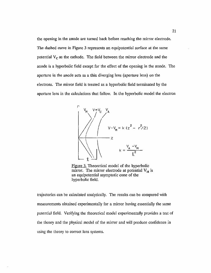
21
the opening in the anode are turned back before reaching the mirror electrode.
The dashed curve in Figure 3 represents an equipotential surface at the same
potential Vc as the cathode. The field between the mirror electrode and the
anode is a hyperbolic field except for the effect of the opening in the anode. 만le
aperture in the anode acts as a thin diverging lens (aperture lens) on the
electrons. The mirror field is treated as a hyperbolic field terminated by the
aperture lens in the calculations that follow. In the hyperbolic model the electron
「
2 2V-VM = k (Z - 「 /2)
Z
V. ..:.v.“k = -"-~:--
A‘
뀐웰똥혹 Theoretical model of the hyperbolicmirror. The mirror electrode at potential VM isan equipotential asymptotic cone of thehyperbolic field.
trajectories can be calculated analytically. The results can be compared with
measurements obtained experimentally for a mirror having essentially the same
potential field. Verifying the theoretical model experimentally provides a test of
the theory and the physical model of the mirror and will produce confidence in
using the theory to correct lens systems.
22
Calculation of the Prooerties of the HvoerbolicElectron Mirror for Svmmetric Ravs
In the theoretical study, the mirror field is considered to be composed of a
hyperbolic field terminated by the aperture lens. Between the anode and mirror
electrode the electron tr떼ectories are calculated from the equation of motion of
the electrons in the hyperbolic field. As the electrons enter and leave the mirror
field they pass through the opening in the anode and are deflected by the
aperture lens. Rays beginning at points on the equipotential surface at cathode
potential are chosen and the intersection (real or virtual) of the electron rays with
the 없is, referred to field-free space outside the mirror, are calculated along with
the angle of intersection as a function of the initial height of the ray. The
electrons leave the cathode potential surface in the mirror field with zero initial
velocity and trace out the path of the symmetric ray. Rays are calculated for a
number of initial heights for a series of values of the ratio of the accelerating
voltage to the mirror voltage. Each voltage ratio corresponds to electrons
traveling to and from a different potential surface in the mirror field. Using these
calculations, as well as an expression for the paraxial object/image distance zo' the
spherical and chromatic aberration coefficients Cs and Cc are obtained.
Electron Trajectories in the Hvoerbolic Field
In the hyperbolic field of the mirror the potential V is given by
V - VM = k(Z2 - r2/2) (19)
where the potential VM replaces V0 of equation (18), and again, rand z are the
(21)
(20)
23
radial and 없ial cylindrical coordinates. The coordinate origin is at the vertex of
the mirror electrode. The coefficient k is equal to (VA -VM)I강 when e is the
없ial length of the mirror field. The equations of motion for the radial and 없ial
components of the electron motion in the hyperbolic field for electron trajectories
lying in meridional planes are:
i' = -(ek/m)r
z = 2(ek/m)z,
where e and m are the charge and mass of the electron, and the second
derivatives with respec i: to time are marked with two dots.
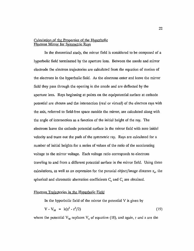
For the symmetric ray, the electron penetrates the hyperbolic field until it
reaches the point (rozd on the potential surface Vo as shown in Figure 4. Here
the velocity components t and z are both zero, and if t is chosen to be zero at
this point the solutions for the electron coordinates and velocity components as a
function of time are:
r = re cos(ωt) (22)
z = ze cosh(12 ωt) (23)
t - -ωre sin(ωt) (24)
z = 12 ωze sinh(12 ωt), (25)
where ω = "J(ek/m). On the cathode potential surface, the coordinates re and ze
satisfy the hyperbolic relation z감 - re2/2 = zea2
• Here zα is the axial coordinate
of the vertex of the potential surface V0 and is given by
Zα,21e2 = (Ve - VM)I (VA - VM) = 1 - v , (26)
24
where v is the ratio of accelerating voltage to mirror v이tage (VA -Vd/(VA-VM).
6α
-‘ ELECTRONTRAJECTORY
~~z
Fi웰I효표£ Trajectory of the symmetric ray in the hyperboIic mirror field.
Because of the symmetry of the trajectory described by (22) and (23) we
will consider only the returning portion of the trajectory.. Beginning at (rozC> on
the surface having potential equal to the cathode potential Ve, the returning
electron reaches the anode at time tAgiven by
rA = rc cos e
ZA = Zc cosh(.f2 e),
(27)
(28)
where e = ωtAo This portion of the path of the electron terminates at the point
(rA>zA) on the hyperb이oid at anode potential. The coordinates are related by the
condition ZA2- r//2 = e2, where e is the length of the mirror field along the Z
axis. A first approximation for e can be obtained by setting ZA = e in equation
(28). With this value of e a first approximation for rAis obtained. Using this
value in equation (27) yields a new value for e which in turn leads to improved
25
values of ZA' 8, and rN For the narrow beams used in electron optics, one
iteration of this sequence is usually enough to provide sufficient accuracy.
When the electron reaches the anode, its velocity components are
t A = -c..>rcsin8 = - ωrAtan 8 (29)
ZA = ..[2 ωzcSinh(..[2 8) =..[2 ωzAtanh(..[28). (30)
The slope of the electron trajectory as it reaches the anode is
tA/ZA = (- rAtan 8)/(..[2 zAtanh(..[2 8» = - tan aN (31)
Here aA is the angle which the tangent to the trajectory makes with the axis prior
to deflection by the aperture lens (see Figure 4).
Deflection bv the Aoerture Lens
ηle focal length for a circular aperture in an electrode can be calculated
by means of the aperture lens formula developed by Davisson-Calbick (D-C) [30].
The D-C formula gives the focal length as
fA = 4 vn/[(aV/&h - (aV/&)d, (32)
where Vn is the beam voltage at the plane of the electrode, and the denominator
is the difference between the potential gradients at the two faces of the electrode
if no aperture were present in the electrode. The D-C formula is good in the
weak lens approximation, where the variation in potential across the aperture is
small compared with the beam voltage of the electrons. Since the anode in the
mirror field is a curved hyperb이ic surface, the aperture appears to act as a thin
meniscus lens on the surface of the anode. At the anode Vn = VA -Vc, (aV/ & h
= 0, and (aV/&)1 = 2 kZA = 2(VA - VM) ZA/e2, from which
fA = - 2[(VA- Vd/(VA- VM)](t2/ZA) = - 2vt/ T1 ,
where T1 = ZA/t = '\J(1 + rA2/2t 2).
26
(33)
The trajectory of an electron passing through the aperture lens is deflected
by an angle
6 = arctan(rA/以) = arctan(-rAT1/2vt).
만Ie deflected trajectory makes an angle
a = aA + 6
= arctan(rAtan e/.f2zAtanh(.f2 e» - arctan(rAT1/2vt)
with the axis in field-free space outside the mirror field. The ray or its virtual
extension intersects the axis at Z according to
(34)
(35)
Z-ZA = rA/tana.A - 'AI
The Paraxial Obiect/lmage Distance and the Sphericaland Chromatic Aberration Coefficients of theMirror
For paraxial rays (36) can be simplified to yield an expression for the
paraxial object or image distance Z。
Zo/ t - 1 = qo = 2v/(.[2v tan eo - 1).
(36)
(37)
The chromatic aberration coefficient is calculated from the variation of z。
with electron energy. For the symmetric ray case, equal amounts of chromatic
aberration !!..,;zo occur on the object and image side of the mirror. Since the
magnification m is equal to unity, the total chromatic aberration, referred to
either object or image space, is (!!..czo)total = 2 !!"czo' The chromatic aberration
coefficient Cc is defined by
27
(dcZo)total = Cc d v/v. (38)
Differentiation of the expression for Zo with respect to v in (38) yields the
following expression for Cc:
Cc!t = - [v/(1 - v)][1 + qo + (3/4)qo2/v2], (39)
with qo as in (38) and for m = 1.
The spherical aberration coefficient Cs is obtained from the variation of
the object or image distance z with the angle a of the rays. The spherical
aberration for symmetric rays is also equally divided between the object and the
image, with dsZ = Z - Zo on each side. The total aberration (dsZ)total is 2dsZ and
the spherical aberration coefficient Cs is defined by
(dsZ)total = - Csa2• (40)
The convention of regarding Cs as positive for the usual case for lenses where
spherical aberration is undercorrected, i.e. for Z - Zo < 0 requires the minus sign
to appear in (40).
The electron mirror properties calculated from the equations developed
here are presented graphically in Figures Sa and Sb, as a function of the voltage
ratio v. The mirror properties are shown only for the first working region, where
the incident and returning electrons cross the axis once.
The normalized par없ial object/image distance zo/ t is plotted in Figure Sa.
The distance Zo is seen to increase continuously as v decreases over the range of
v plotted. For v closer to 1.0 than shown, the electrons cross the axis more than
once. For v near 0.6, the mirror becomes diverging. The transition from the
28
-160
-140
-120。《
\ -100(J
u• -80
eX\ -60
ulu-40 에 / 1""'/ ~ 2 UJ
U-20 I- “〈ζ
---------t 1 \
LJ
o ’ { LJ oU0.7 1. 0 0.9 0.6 0.7
V
g
뚫j46 1-
\ 4。
N3
g
i
o1. 0 0.9 0.6
V
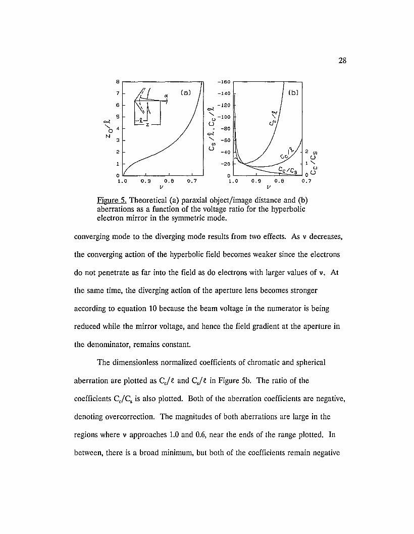
Fi웰I료혹 Theoretical (a) par없ial object/image distance and (b)aberrations as a function of the voltage ratio for the hyperbolicelectron mirror in the symmetric mode.
converging mode to the diverging mode results from two effects. As v decreases,
the converging action of the hyperb이ic field becomes weaker since the electrons
do not penetrate as far into the field as do electrons with larger values of v. At
the same time, the diverging action of the aperture lens becomes stronger
according to equation 10 because the beam voltage in the numerator is being
reduced while the mirror voltage, and hence the field gradient at the aperture in
the denominator, remains constant.
The dimensionless normalized coefficients of chromatic and spherical
aberration are plotted as Ce/ e and Cs/e in Figure 5b. The ratio of the
coefficients Cc!Cs is also plotted. Both of the aberration coefficients are negative,
denoting overcorrection. The magnitudes of both aberrations are large in the
regions where v approaches 1.0 and 0.6, near the ends of the range plotted. In
between, there is a broad minimum, but both of the coefficients remain negative
29
while their ratio continues to change monotonically.
The reason that the hyperbolic mirror has overcorrected aberration
properties can be understood qualitatively as follows. The hyperbolic field
produces converging action which depends both on the radial force on the
electron, which is proportional to the distance from the axis, and on the time
which the electron spends in the field. For chromatic aberration, the lower
energy electrons penetrate less far into the field than do higher energy electrons.
Lower energy electrons spend less time in the field and are consequently less
strongly converged by the field. The action of the aperture lens on the other
hand, is more strongly diverging for lower energy electrons. These two effects
combine causing the focal distance to be longer for low energy electrons than for
high energy electrons. For spherical aberration, electrons entering the mirror off
axis do not penetrate as far into the field. Consequently they spend less time in
the hyperbolic field than do paraxial electrons. Thus the converging action is
weaker for them, which makes the focal distance longer for off-axis rays than for
paraxial rays.
We can now understand why the aberration coefficients increase as v
approaches 1.0. The time electrons spend in the mirror field depends on the
electron energy and the angle ex which the trajectory makes with the axis. For an
electron traveling along the axis, the time which it spends in the field approaches
∞ as v approaches 1.0. A less energetic electron or an off-axis electron of the
same energy spends a finite time in the field. The result is that both chromatic
30
and spherical aberrations increase dramatically for the voltage ratio approaching
1. The aberration coefficients also become large as v approaches 0.6. Here Zo is
large, as shown in Figure Sa, and ex is small; consequently small aberrations in the
trajectories produce relatively large longitudinal aberrations. In addition, for the
spherical aberration coefficient, a given longitudinal aberration !u produces a
larger increase in the aberration coefficient when ex is small since Cs = -Jlzjex2•
In matching the over-corrected aberrations of the mirror to the
undercorrected aberrations of a lens or lens system, there are three mirror
parameters at our disposal. The voltage ratio v of the mirror, the scale of the
mirror, and the magnification of the image to which the mirror correction is
applied can all be chosen to effect the match. The ratio of the aberration
coefficients, as well as their magnitudes, varies as a function of the voltage ratio
v, as shown in Figure Sb. The mirror scale, voltage ratio, and magnification must
be adjusted in a coordinated way in order to achieve simultaneous correction of
chromatic and spherical aberration. Other parameters, associated with the
electron optical system to be corrected, include the design and relative scale of
the lenses, and their voltage ratios which in turn determine the magnitude of
chromatic and spherical error to be corrected.
CHAPTER III
CORRECTIONOFCHROMATICABERRATIONWIlli AN ELECfRON MIRROR1
INTRODUCTION
Electron mirrors have chromatic and spherical aberration coefficients of
opposite sign from those of electron lenses and, in principle, can be used to
compensate the spherical and chromatic aberrations of electron lens systems
[7,20,22,24]. A method of implementing a hyperbolic electron mirror as an
aberration corrector in electron microscopes has been proposed recently [28].
Correction of chromatic aberration is of particular interest in the case of emission
electron microscopes and related low-energy electron microscopes, where the
accelerating field has a large chromatic aberration coefficient [2,3], and also in
probe-forming instruments, especially focused ion beam instruments, where the
energy spread is large [1]. In the present paper we report the experimental
verification of the correction of chromatic aberration by means of a hyperbolic
electron mirror.
1 The contents of this chapter are reproduced from Ref. 31 with permission ofthe co-author. Minor editing, including renumbering figures and references, wasrequired to harmonize with the text of the dissertation.
32
THE ELECTRON OP1’ICALSYSTEM
The electron optical arrangement described in ref. [28] is used in the
experimental study. The conditions leading to aberration correction are
investigated with the optical system operating in the probe mode, shown
schematically in Figure 6. πle object for the optical system is the exit pupil (or
crossover) of the electron gun. The final image formed by the optical system is a
demagnified image of the crossover. Aberration correction is provided by the
hyperb이ic mirror at the left of the diagram. The electron beam enters the mirror
from the right, and is reflected at a curved equipotential surface of the mirror
field. The incident and reflected beams are centered on the mirror axis. The
mirror is operated in its converging range, and in the symmetric mode, i.e., with
object and image distances equal.
In order to independently control the electron beams headed toward and
away from the mirror it is necessary to use a beam separator in conjunction with
the mirror. ’The beam separator used in our experiments and described in ref.
[28] consists of three magnetic deflectors, two pairs of relay lenses, and an
interface lens. The magnetic deflector on the mirror axis performs the function of
splitting the incident and reflected beams apart; the other deflectors bend the
incident and reflected beams so that their axes are parallel with the mirror axis.
A key feature of the beam separator is that deflections take place at image
planes, which largely avoids the detrimental effects of deflection aberrations. The
33
Condeneer‘Lene
Mirror Inter‘ faceLene
ElectronSource
\
좌인
매
/
때빼뼈H
Obj ecU veLene
뼈it’
a)
|
腦iu--‘D
뀐웰뜨효: ’The electron optical arrangement used for theexperimental study of aberration correction by an electron mirror.The electron source (upper right) seπes as the 0비ect for thesystem. Aberrations in the demagnified image of the source (lowerright) are investigated by means of the shadows cast by a fine meshclosely following (or preceding) the image. Aberration correction isprovided by the hyperbolic mirror at the left of the diagram.Separation of the beams heading toward and away from the mirroris accomplished by a beam-separator consisting of three magneticdeflectors (at image planes), two pairs of relay lenses, and aninterface lens.
relay lenses are used to transfer the image between deflectors. Several other
features further reducesensitivity to deflection aberrations: the images at the
deflection planes are magnified; the image is transferred between deflectors in
parallel orientation; the two deflections in each branch are in opposite senses with
respect the image; and the deflection angle is fairly small (about 16°). The
interface lens enables the use of magnified images at the deflection planes and
seπes to balance aberrations by acting as a magnification interface between the
objective lens and the mirror. The interface lens is operated in zoom fashion with
34
the mirror to keep the images centered in the deflectors during adjustment of the
mirror voltage.
METHOD OF DETERMINING ABERRATIONS
The method of investigating the aberrations in the final image of Figure 6
is based on the grating shadow method of ref. [32]. In the present experiments a
fine mesh rather than a bar grating is used to enable us to detect the presence of
astigmatism. The mesh is placed closely following (or preceding) the image, and
casts a highly-magnified shadow on a phosphor screen. The shadow is used to
determine the image aberrations. The geometrical relation between the shadow
magnification M' and the image distance z’ is illustrated in Figure 7. With the
mesh located downstream from the image, as in the diagram, and at a distance d
from the phosphor screen, the distance c from the image to the mesh is given by
(c + d)/c = E까’ =M’, where e' is the height of the ray at the mesh, and E' is
the height of the shadow. Solving for c gives
c = d/(M’ - 1). (41)
The distance of the image from the lens is then obtained from z’ = b - c, where b
is the distance of the mesh from the lens.
In general the image exhibits some spherical aberration, which manifests
itself as a change in shadow magnification as a function of the height p of the ray
at the lens, or the angle a’ at which the ray goes through the image. A plot of
(M’ - 1)"1 versus p2 leads to the pa따n‘a때1
35
까|E
~」
c d
Fi웰I흐그~ Diagram illustrating the relation between the magnificationof the shadow cast by the mesh and the location of the image formedby the objective lens.
distance. The slope of this plot can also be used to determine the longitudinal
spherical aberration Asz’ in the image.
To test for chromatic aberration a small voltage increment AVa is added to
the accelerating voltage Va (independently of the lens and mirror voltages), and
the change in magnification of the shadow pattern is used to determine the
longitudinal chromatic aberration Ac;Z' of the paraxial image. From equation (41)
the longitudinal aberration is
Ac;Z' = - Ac = c[A(M’ - 1)]/(M’ - 1) = cAM’/(M’ - 1). (42)
(For a mesh upstream from the image the signs of M’ and C, and the type of
shadow distortion, are reversed.) The resultant chromatic aberration coefficient
for the system is
Cc = Ac;Z’/(AVa/Va)' (43)
36
In the case of undercorrected aberration, Z’ increases as the accelerating voltage
increases, and Cc is positive. If the mesh is downstream from the image, as in
Figure 7, the shadow magnification increases. The opposite is true for
overcorrected chromatic aberration.
The definition of the chromatic aberration coefficient given by equation
(43) is based on the longitudinal chromatic aberration in the image. An
alternative definition for the chromatic aberration coefficient is based on the
radius of least confusion referred to object space, rtc = Cc(dVjV)a [33]. In
balancing the aberrations of the optical components in a system it is important to
be consistent, because the alternative definition gives a value which is one-half of
the value given by equation (43). We find equation (43) to be more meaningful
and useful than the alternative definition because the longitudinal aberrations
carry plus or minus signs and are the quantities which must cancel for aberration
correctIon.
The correction of the final image of Figure 6 depends on the cancellation
of the lens aberrations by the mirror aberrations. The aberrations of the relay
lenses and the condenser lens can be ignored if the magnification of the image on
which they operate is sufficiently high relative to the magnification of the image in
the mirror stage. In this case the mirror need compensate only the aberrations
due to two imagings by the interface lens and one imaging by the objective lens,
and the condition for correction of chromatic aberration is
CcM + 2 Cc2 +(m1m2)2Ccl = o. (44)
37
The subscripts 1 and 2 denote the objective and interface lenses, respectively, and
M denotes the mirror. The lens aberration coefficients are referred to the low
magnification sides of the lenses: the probe side of the objective lens, and the
mirror side of the interface lens. The magnifications m1 and m2 are defined for a
beam directed from the objective stage to the mirror. For this direction of the
beam m1 is greater than 1, and m2 is less than 1. The product m1m2 is the
magnification of the image in the mirror stage relative to the probe, and is usually
not very different from unity in our experiments.
APPARATUS
The experimental study was carried out in a horizontal electron optical
bench. The cover of the bench is a removable glass plate, which enables access
to, and viewing of, the experiment. The bench was modified to include a double
V-way section to support the optical components for the separated branches of
the incident and reflected beams. The electron source (a thermionic triode gun)
and condenser lens were supported on one track, and the objective lens and the
fine-mesh assembly on the other track. A horizontal Y-shaped block was
provided to hold the relay lenses. The interface lens and the mirror were
supported on a single V-way. The magnetic deflectors were located at the
intersections of the relay axes with the axes of the mirror and the condenser and
objective branches. All of the lenses were electrostatic. The accelerating voltage
was 15 kV. The lens voltages were obtained by means of a voltage divider from

38
the high voltage power supply used for acceleration. ’The mirror bias was
obtained from an auxiliary isolated power supply connected to the negative
terminal of the accelerating voltage supply. 까le bias was adjustable from 0 to - 5
kV. The magnetic deflecting fields were produced by electromagnetic coils. The
required voltages and currents were supplied through feedthroughs at the back
and at the left end of the bench. A manipulator on the front of the bench was
used to move the fine-mesh assembly along the objective axis for optimum
adjustment and to ensure that the placement of the mesh, upstream or
downstream from the image, was correctly identified. The shadow patterns cast
by the mesh were received on a phosphor-coated fiber-optics output window at
the right end of the bench, and recorded by a video camera. The operating
pressure in the bench was about 5X lO-5 torr (6.5X lO-3 pa). A photograph of the
optical bench is shown in Figure 8.
An engineering drawing of the hyperb이ic mirror used in the present
experiments is shown in Figure 9. The negative, or mirror, electrode has the
shape of the conical asymptotic equipotential surface of the hyperbolic field. The
mirror electrode is biased negatively with respect to the cathode of the electron
gun, and electrons are reflected at curved equipotential surfaces in front of the
electrode. The small opening at the vertex of the mirror electrode is for beam
alignment. The anode has the curvature of a hyperbolic equipotential surface
except for the beam-opening on the axis. The effect of the anode opening is to
create a thin diverging lens. The length eM from the vertex of the mirror
39
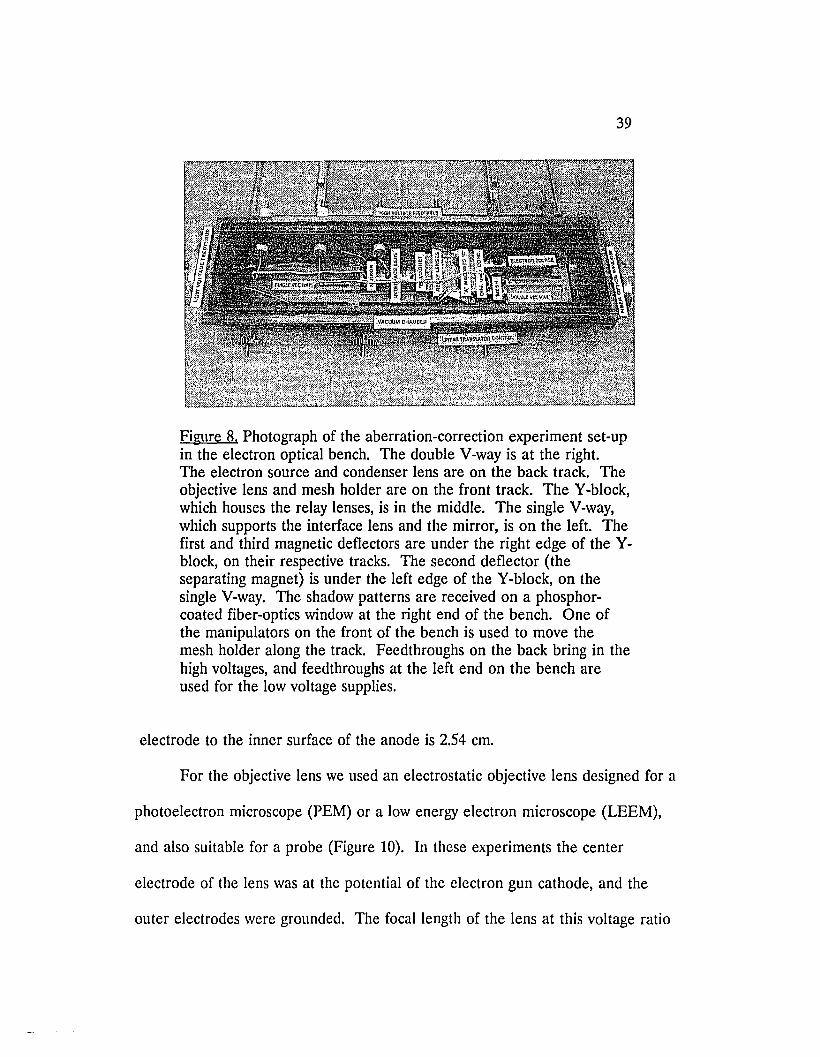
Figur료효. Photograph of the aberration-correction experiment set-upin the electron optical bench. The double V-way is at the right.The electron source and condenser lens are on the back track. Theobjective lens and mesh holder are on the front track. The Y-block,which houses the relay lenses, is in the middle. The single V-way,which supports the interface lens and the mirror, is on the left. Thefirst and third magnetic deflectors are under the right edge of the Yblock, on their respective tracks. The second deflector (theseparating magnet) is under the left edge of the Y-block, on thesingle V-way. ’The shadow patterns are received on a phosphorcoated fiber-optics window at the right end of the bench. One ofthe manipulators on the front of the bench is used to move themesh holder along the track. Feedthroughs on the back bring in thehigh voltages, and feedthroughs at the left end on the bench areused for the low voltage supplies.
electrode to the inner surface of the anode is 2.54 em.
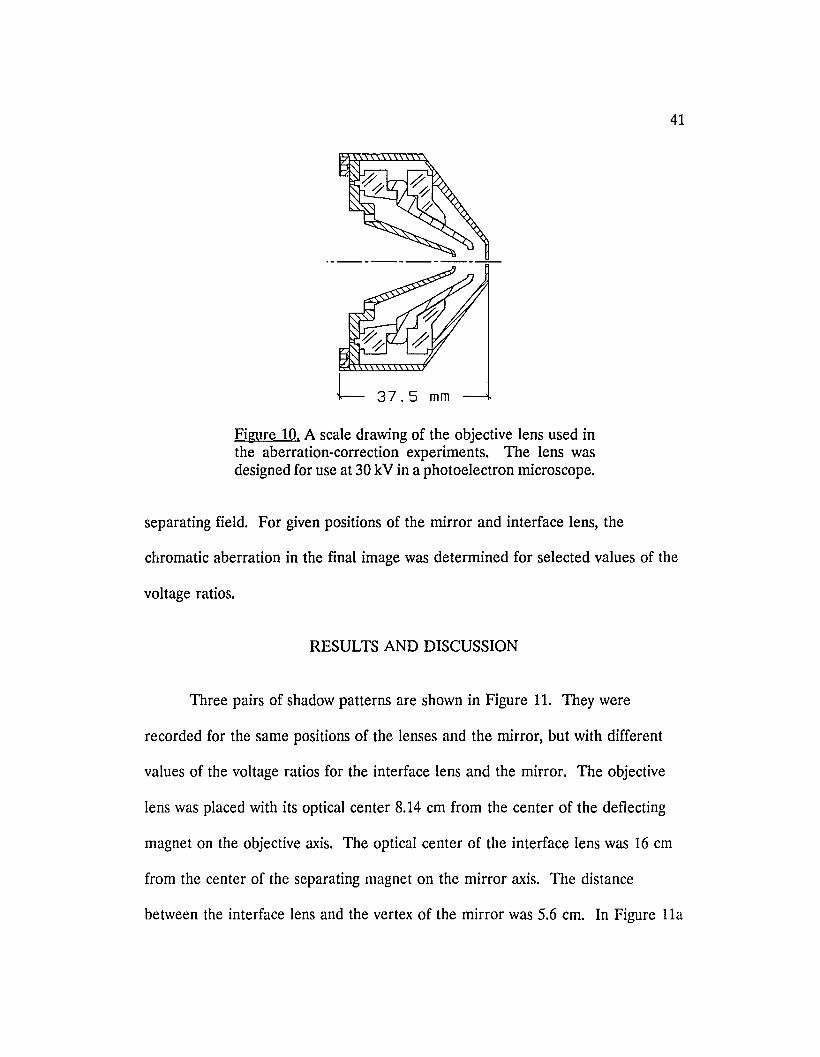
For the objective lens we used an electrostatic objective lens designed for a
photoelectron microscope (PEM) or a low energy electron microscope (LEEM),
and also suitable for a probe (Figure 10). In these experiments the center
electrode of the lens was at the potential of the electron gun cathode, and the
outer electrodes were grounded. The focallength of the lens at this voltage ratio
51 mm
40
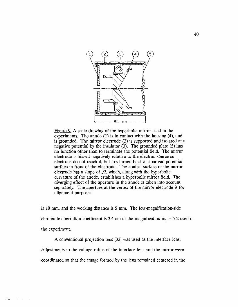
뀐웰또요~ A scale drawing of the hyperbolic mirror used in theexperiments. π1e anode (1) is in contact with the housing (4), andis grounded. The mirror electrode (2) is supported and is이ated at anegative potential by the insulator (3). The grounded plate (5) hasno function other than to terminate the potential field. The mirrorelectrode is biased negatively relative to the electron source soelectrons do not reach it, but are turned back at a .curved potentialsurface in front of the electrode. The conical surface of the mirrorelectrode has a slope of J2, which, along with the hyperboliccurvature of the anode, establishes a hyperbolic mirror field. Thediverging effect of the aperture in the anode is taken into accountseparately. The aperture at the vertex of the mirror electrode is foralignment purposes.
is 10 mm, and the working distance is 5 mm. The low-magnification-side
chromatic aberration coefficient is 3.4 cm at the magnification mt = 7.2 used in
the experiment.
A conventional projection lens [32] was used as the interface lens.
Adjustments in the voltage ratios of the interface lens and the mirror were
coordinated so that the image formed by the lens remained centered in the
41
L 37.5 mm
Filrnre 10. A scale drawing of the objective lens used inthe aberration-correction experiments. The lens wasdesigned for use at 30 kV in a photoelectron microscope.
separating field. For given positions of the mirror and interface lens, the
chromatic aberration in the final image was determined for selected values of the
voltage ratios.
RESULTS AND DISCUSSION
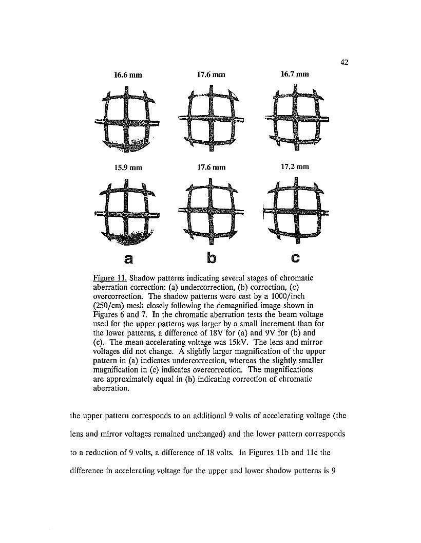
Three pairs of shadow patterns are shown in Figure 11. ’They were
recorded for the same positions of the lenses and the mirror, but with different
values of the voltage ratios for the interface lens and the mirror. The 0비ective
lens was placed with its optical center 8.14 cm from the center of the deflecting
magnet on the objective axis. The optical center of the interface lens was 16 cm
from the center of the separating magnet on the mirror axis. The distance
between the interface lens and the vertex of the mirror was 5.6 cm. In Figure lla
16.6mm
15.9mm
a
17.6mm
17.6mm
b
16.7mm
17.2mm
용
42
Figure 11. Shadow patterns indicating several stages of chromaticaberration correction: (a) undercorrection, (b) correction, (c)overcorrection. The shadow patterns were cast by a IOOO/inch(250/cm) mesh closely following the demagnified image shown inFigures 6 and 7. In the chromatic aberration tests the beam voltageused for the upper patterns was larger by a small increment than forthe lower patterns, a difference of l8V for (a) and 9V for (b) and(c). 단Ie mean accelerating v이tage was 15kV. The lens and mirrorvoltages did not change. A slightly larger magnification of the upperpattern in (a) indicates undercorrection, whereas the slightly smallermagnification in (c) indicates overcorrection. πIe magnificationsare approximately equal in (b) indicating correction of chromaticaberration.
the upper pattern corresponds to an additional 9 volts of accelerating voltage (the
lens and mirror voltages remained unchanged) and the lower pattern corresponds
to a reduction of 9 volts, a difference of 18 volts. In Figures lIb and lIe the
difference in accelerating voltage for the upper and lower shadow patterns is 9
43
volts rather than 18 volts. A 1000 squares/inch (394/cm) mesh was located
downstream from the image, and at a distance of 37 em in front of the phosphor
screen. The diameter of the shadow patterns shown corresponds to 2.7 em on the
phosphor screen. The average paraxial shadow magnification at the phosphor
screen was 333. From equation (41), the distance from the image to the mesh
was 0.111 em. The pair of shadow patterns on the left (Figure 11a) shows a
slightly larger magnification in the upper pattern than in the lower pattern,
indicating that the image moved forward (i.e., away from the lens) as the beam
voltage was increased and that the chromatic aberration was undercorrected. The
magnification difference is about 4.3%. From equation (42), A(Z.' = 48 μm, and
from equation (43), Cc = (48 μm)/(18/15X10 3) = 4.0 em. The patterns in the
center (Figure lIb) have approximately equal magnifications, indicating that
chromatic aberration is approximately corrected. On the right (Figure 11c), the
magnification of the upper pattern is 3% smaller than that of the lower pattern,
indicating that the image moved backward (toward the lens) as the voltage was
increased and that the chromatic aberration was overcorrected. In this case Ac'Z’
= - 33 μm, and Cc = (-33 μm)/(9/15Xl 앤) = - 5.6 em. The v띠tage ratios and
magnifications for the mirror and the interface and objective lenses corresponding
to the three sets of patterns in Figure 11 are given in Table I.
The barrel-type distortion in the shadow patterns of Figure 11 indicates
that the image has undercorrected spherical aberration. However, a substantial
amount of spherical aberration correction accompanies the chromatic aberration
44
correction. For comparison, considerably more distortion can be seen in the
shadow pattern of Figure 12, which was obtained with the objective lens alone
(without the correcting system) under otherwise similar conditions. The lower
distortion in Figure 11 makes it feasible to position the mesh closer to the image,
and to use smaller voltage increments for exploring chromatic aberration. Some
asymmetry in the shadow patterns occurs because there was no provision for
centering a mesh opening or intersection on the optical 없is.
Cancellation of the chromatic error, as evidenced by the shadow patterns
of Figure lIb, amounts to correcting an electron probe having the configuration
used in the experiment. This same method of investigating the conditions for
chromatic aberration correction can be applied to a transmission electron
microscope (TEM) with the electrons traveling backward through the system and
focusing to a probe in the specimen plane, as in Figure 6, but with an objective
lens suitable for a TEM. If the specimen plane is immersed in a magnetic field,
as is usual in electromagnetic TEMs, the effect of the magnetic field on the
shadow patterns will need to be taken into account. However if the specimen
plane is in field-free space the shadow pattern analysis of Section 3. can be
applied directly. In the case of emission electron microscopes and related low-
energy electron microscopes, the specimen is the cathode of an accelerating field,
and correction of the final image of Figure 6 would still leave the aberrations of
the accelerating field uncorrected. For correction of this type of microscope, the
45
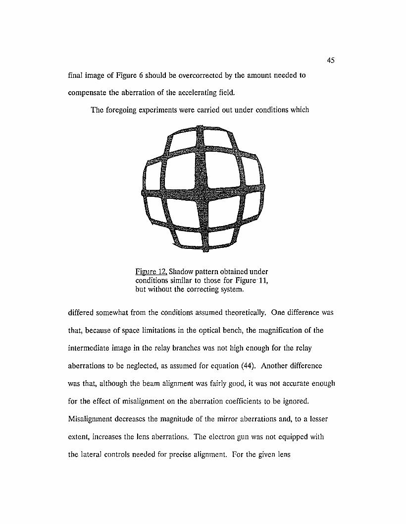
final image of Figure 6 should be overcorrected by the amount needed to
compensate the aberration of the accelerating field.
The foregoing experiments were carried out under conditions which
Filmre 12. Shadow pattern obtained underconditions similar to those for Figure'II,but without the correcting system.
differed somewhat from the conditions assumed theoretically. One difference was
that, because of space limitations in the optical bench, the magnification of the
intermediate image in the relay branches was not high enough for the relay
aberrations to be neglected, as assumed for equation (44). Another difference
was that, although the beam alignment was fairly good, it was not accurate enough
for the effect of misalignment on the aberration coefficients to be ignored.
Misalignment decreases the magnitude of the mirror aberrations and, to a lesser
extent, increases the lens aberrations. The electron gun was not equipped with
the lateral controls needed for precise alignment. For the given lens
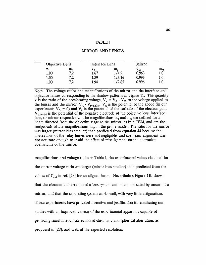
46
TABLE I
MIRROR AND LENSES
Obiective LensVI m l1.00 7.21.00 7.21.00 7.2
Interface Lens MirrorV2 m2 VM mM1.67 1/4.9 0.963 1.01.89 1/3.16 0.993 1.01.94 1/2.85 0.996 1.0
Note. The voltage ratios and magnifications of the mirror and the interface andobjective lenses corresponding to the shadow patterns in Figure 11. The quantityV is the ratio of the accelerating voltage, Va = VA - Vo to the voltage applied tothe lenses and the mirror, VA - Vi=I,2,M' VA is the potential of the anode (in ourexperiments VA = 0) and Vc is the potential of the cathode of the electron gun;VI,2,or M is the potential of the negative electrode of the objective lens, interfacelens, or mirror respectively. The magnifications ml and m2 are defined for abeam directed from the objective stage to the mirror, as in a TEM, and are thereciprocals of the magnifications mlo in the probe mode. The ratio for the mirrorwas larger (mirror bias smaller) than predicted from equation 44 because theaberrations of the relay lenses were not negligible, and the beam alignment wasnot accurate enough to avoid the effect of misalignment on the aberrationcoefficients of the mirror.
magnifications and voltage ratios in Table I, the experimental values obtained for
the mirror voltage ratio are larger (mirror bias smaller) than predicted from the
values of CcM in ref. [28] for an aligned beam. Nevertheless Figure lIb shows
that the chromatic aberration of a lens system can be compensated by means of a
mirror, and that the separating system works well, with very little astigmatism.
These experiments have provided incentive and justification for continuing our
studies with an improved version of the experimental apparatus capable of
providing simultaneous correction of chromatic and spherical aberration, as
propose 이 in [28], and tests of the expected resolution.
CHAPTERIV
SIGNIFICANCE OF RESULTS
Using the mirror to correct chromatic aberration in an electron optical
system but without fully compensating spherical aberration: what results can be
anticipated? The two most common figures of merit for optical systems are
resolution and intensity. Correction of aberrations will improve resolution and
increase the intensity available at the output of electron optical systems. The
magnitude of the benefit will depend upon the relationship between the size of
the aberrations and the resolution in the system in question. In this chapter, three
examples of electron optical systems will be examined in some detail for the
expected benefits of the correction of chromatic aberration.
One measure of resolution in light instruments is the Rayleigh criterion
which states that two adjacent equally luminous image points are just resolved if
the intensity in their overlapping patterns drops by about 25% of the peak
intensity of either point. This criterion is also used to evaluate resolution in
electron optics. Another method of evaluating resolution is the Taylor’s criterion
where the resolution between two overlapping luminous points is defined to be
the distance between the peaks which causes the sum of the overlapping
intensities to be equal to half of the intensity at the peak.
48
According to the geometric theory of resolution developed by Rempfer and
myself [33], the image of a small uniformly illuminated disc object is a peaked
cone in the plane of best focus. ’The half-maximum diameter of the intensity
pattern referred to 0피ect space is nearly equal to the diameter of the 0비ect. The
intensity of the peak also increases with the size of the object. However, the
intensity of the maximum is reduced by the effect of aberrations. Resolution and
intensity are seen to be related in this theory in that, in finite-time microscopy the
illumination in the image peak must be sufficient that a non-noisy image can be
recorded in the allotted exposure time. Under the Rayleigh criterion, the
resolution turns out to be roughly equal to the diameter of the smallest object
supplying the required illumination in the image peak. 까le question of limiting
resolution in electron optics frequently becomes one of image contrast in the
presence of background illumination. For an image to be seen, it must rise above
the background illumination. A contrast requirement which is often used is that
in order for two luminous points to be resolved, their overlapping intensities
added to the background must drop by 10% of the maximum intensity of one
peak added to the background. The technique developed in reference [33] to
calculate the intensity in the image will be used to evaluate the geometrical
resolution results for the following cases.
49
TRANSMISSION ELECTRON MICROSCOPE
One of the 이dest and most familiar electron optical instruments is the
transmission electron microscope (TEM). In this case the spacial resolution in
the image is of primary importance. Intensity in the final image is usually
adequate, being supplied by an electron source and not the specimen itself. In
the example given for resolution limited by diffraction in Chapter I, a 60 kV beam
of electrons has a wavelength of .05 A and, with an angular aperture of 0.01 rad.,
yields a resolution of about 3 A in an electron microscope. Since the aberration
limited resolution is much larger than the ultimate diffraction limit of 0.61λ/sin a
= 0.03 A, the benefits of reducing the magnitude of aberrations would be
expected to benefit the resolution.
In order to apply any criterion to the image of a luminous object in the
TEM, it is necessary to know how aberrations affect the distribution of intensity.
This relationship is supplied by the geometrical theory of resolution. In
calculating TEM resolution directly more information about the specifIc imaging
conditions of contrast and detection limits would have to be known. In order to
estimate the improvement expected from eliminating chromatic aberration for a
given imaging condition however, the situation is less difficul t. In the plane of
best focus the current in the image of a uniformly illuminated element of radius
= R, formed by a lens system of spherical aberration Cs with a single energy
beam, is
I ex 1.2 R8/3 (4/Cs)2/3.
so
Whatever the particular conditions under consideration are, the intensity will be
smeared out along the axis by the chromatic error, lowering the value of current
contained in the smallest resolved image. Knowing the reduction in current, the
resulting effect on resolution can be estimated by solving this relationship for the
new value of R containing the same intensity formerly producing sufficient
contrast to constitute the resolution limit. If instead, the resolution element R is
resolved in the presence of chromatic aberration and we ask what smaller value of
R would contain the same current in the absence of chromatic aberration, we may
estimate this improvement from the same equation if we know the amount by
which the current is increased.
Spherical error also smears the image of each point in the object out along
the axis in the image. 까Ie technique described in reference [33] allows the
intensity distribution in the image of a geometrical resolution element to be
calculated in the presence of spherical error. The effect of chromatic aberration
is to further smear each monochromatic image plane along the axis by an amount
dz given by dz = Cc dVIV where Cc is the chromatic aberration, dV is the change
in beam voltage, and V is the beam voltage. For a thermionic source of electrons
dV might be 0.5 volt. With a beam voltage V = 40 kV, and Cc = 1.2 cm, dz =
1500 A. In this case the spherical aberration constant is equal to 4 cm and a 5 A
radius resolution element would have maximum intensity imaged in the plane of
best focus. This plane would be displaced from the paraxial image plane by about
4070 A. The reduction in peak intensity for a further displacement of the image
51
along the axis caused by chromatic error would result in a decrease of peak
intensity in the image to about 58% of that in the plane of best focus.
Conversely, eliminating chromatic error from a system suffering from chromatic
error should result in an increase in intensity of 1/.58 = 1.71 times the peak
intensity in the plane of best focus. ’The intensities are smeared along the 값is by
chromatic error reducing the peak intensity but not appreciably widening the
distribution. We may then take the increase in peak intensity to calculate a new
resolution R from the relationship for the total current in the element just
resolved by the system. An increase in intensity of 1.71 corresponds to an
improvement of resolution from 10 Ato about 8.2 A. Thus, only a modest
improvement for an electron microscope results from correcting chromatic
aberration due to the energy distribution in the electron source. However, if the
energy distribution due to scattering by the specimen is considered, a much larger
benefit could be expected.
EMISSION MICROSCOPE
In the case of emission microscopy the specimen emits electrons or ions
under the influence of illumination by photons or bombardment by electrops or
ions. The specimen is placed in an electric field and the emitted electrons are
accelerated and imaged at magnification with an optical system much the same as
in the case of the TEM. The presence of the accelerating field introduces both
undercorrected spherical and chromatic aberrations. The magnitude of the
52
chromatic aberration for the accelerating field is of the same order as the
objective lens aberration but the chromatic error of the field can be much larger
than that due to the lens, particularly in the case of small emission energies.
These aberrations add to those of the objective and other lenses in the system
further limiting the final resolution. In the photoelectron microscope (PEM) [2],
the present practicallimit of the microscope is about 100 A. Theoretical
considerations set the diffraction limit to about 20 A. Depending upon the
emission energy of the photoelectrons, the benefits of correcting chromatic
aberration alone may range from improving the resolution to 30 A at low
emission energies and good contrast to 80-90 A with higher emission energies and
poor contrast. For the PEM where many biological structures lie in a range of
sizes near the theoretical resolution limit, any improvement in resolution would be
welcome. Implementing the mirror as described in this study in such a system
would already provide some compensation of spherical error. Most likely any
attempt to add the mirror to an emission microscope would seek to correct both
aberrations simultaneously thereby realizing the full capability of the microscope.
ELECfRON OR ION PROBE
The electron and ion probes are instruments designed to produce a small
focussed beam of electrons or ions. The optics of the probe are distinguished
from the TEM in that it is usually necessary to have the probe focussed at some
distance from the final lens in order to accommodate some other equipment. By
53
requiring the finallens to have a large working distance, the resulting aberrations
of the lens are greatly enlarged. An electrdstatic probe lens having a working
distance of 5 em and operating at unity rna당nification might have spherical
aberration Cs = 400 cm and chromatic abeLTation Cc = 40 cm. If the source of
current has a radius of 75 A then in the plane of best focus the image of about 75
A in half width will contain a current limited by the spherical error. The 없ial
displacement of the image produced by a voltage spread in the source of 0.5 volt
in a beam voltage of 10 kV will be 2 x lOS A. A shift in the image of this
magnitude would reduce the peak current to 37% of the value in the plane of best
focus. Furthermore, with such a large chromatic aberration in this plane the
image would be spread out to the place where the half width was four times the
original size with a very slowly diminishing tail spreading current well beyond the
desired image. The benefit of eliminating the chromatic aberration is too large to
estimate using this method. By superimposing a number of image planes
corresponding to monochromatic images of ithe source, the spread in chromatic
differences could be made small enough fori each plane to form an integrated
total image of the source and thl~ result of eliminating chromatic aberration
estimated. Given the rather slowly varying character of the image peak with axial
location due to the large spherical error, and the peaked nature of the Maxwellian
distribution of current from a thβrmionie source, I would expect a nearly linear
increase in current in the image with respect to reduction of chromatic error.
Attempting to estimate the resolution by comparing the areas under graphs of the
54
intensity distributions, I would expect an order of magnitude increase in current
into the image in the plane of best focus by eliminating the chromatic aberration.
’The trend toward lower energy probes in several areas of biological and
semiconductor research suggests that this would be a project worthy to pursue.
Whatever the benefits are in the example examined here, the benefits will be
larger as the beam voltage is further reduced.
CONCLUSION
In these three examples: the TEM could benefit from correction of
chromatic aberration due to the electron energy spread caused by inelastic
scattering by the specimen; the emission microscope would also benefit
significantly because of the large chromatic aberration coefficient of the
accelerating field; and the probe would receive enormous benefit due to the large
chromatic coefficients of the lenses needed to obtain the required working
distance. The magnitude of the chromatic error relative to the limiting resolution
was the determining factor in evaluating the potential improvement available.
Since the chromatic error scales up proportional to the focal length of electron
lenses, one could anticipate that everywhere that long focal lengths are required
in electron optics, resolution would be limited to aberrations and there would be
potential benefit for using a mirror to correct the chromatic aberration. Besides
the probe, electron optical systems with long focal lengths are found in ion
implanters, mass spectrometers, surface ion mass spectrometers (SIMS), electron
55
energy loss spectrometers (EELS) of a variety of forms, electron beam furnaces
and welders, image converters, vidicons, cathode ray tubes (CRT), and television
display tubes. It seems reasonable that these instruments would be potentially
eligible for adaptation to mirror correction of chromatic aberration in the form
presented in this work. The greatest motivation for the correction of aberration
in any of the systems mentioned would be where increased sensitivity or
resolution lies at the threshold of important new information as in the case of the
PEM. ’The correction of chromatic aberration alone would seem to be most
beneficial in those cases where the chromatic error was the major resolution
limiting factor. All probes meet this test. Improvement in the resolution of
probes to the limit of spherical error can be achieved with the mirror as used in
this study. Ion probes, where the ions are formed with a large energy spread, are
even better candidates for the correction of chromatic aberration. Many of the
analytical instruments also meet this criterion. There is constant need to improve
instrument sensitivity in order to solve increasingly more difficult problems lying
at the threshold of detection. Detecting the presence or effects of contaminants
in the environment continues to challenge instrumentation to detect at ever
smaller limits. Every increment in improving the sensitivity of these instruments
permits the exploration of previously undetectable conditions. The mirror,
implemented as it was used in this study, can provide immediate benefit to a
many of these needs.
REFERENCES
[1] L. W. Swanson, G. A. Schwind, and A. E. Bell, J. Appl. Phys. 51 (1980) 3453.
[2] G. F. Rempfer and O. H. Griffith, Ultramicroscopy 27 (1989) 273.
[3] O. H. Griffith and W. Engel, Ultramicroscopy 36 (1991) 1.
[4] W. H. Fincham, Optics (Hatton Press, London, 1956) pp. 240-241.
[5] M. Herzberger, Modern Geometrical Optics (Interscience Publishers, London,1958) pp. 112-113.
[6] Von W. Henneberg and A. Recknagel, Zeitschr f. Physik 12 (1935) 621.
[7] A. Recknagel, Z. Phys. 104 (1936) 381.
[8] Von G. Hottenroth, Ann. der Physik 30, no. 5 (1937) 689.
[9] W. Henneberg, U. S. Patent No. 2,161,466 (6 June 1939).
[10] V. K. Zworykin, G. A. Morton, E. G. Ramberg, J. Hillier, and W. A. Vance,Electron Optics and the Electron Microscope (Wiley, New York, 1945). Seeespecially pp. 456-464, 630-631, and 645.
[11] O. Scherzer, Zeit. f. Phys. 101 (1936) 593.
[12] O. Scherzer, Optik 2 (1947) 114.
[13] H. Koops, Proc. 9th Intern. Congr. on El. Microscopy, ed. 1. M. Sturgess(Microsc. Soc. of Canada, Toronto, 1978), III 185.
[14] A. V. Crewe and D. Kopf, Optik 55 (1980) 1-10.
[15] L. R. Harriott, W. L. Brown, and D. L. Barr, Am. Vac. Soc. 8, no. 6, (1990)1706.
[16] G. M. Fleming, U. S. Patent No. 2,740,919 (3 April 1956).
57
[17] M. Kuzuya, T. Hanai, M. Hibino, and S. Maruse, J. E l. Micr. 31, no. 1 (1982)18-26.
[18] P. W. Hawkes, Adv. in Electronic and Electron Phys. SuppI., ed. A. Septier(Academic, New York, 1980), 13A, 109-140.
[19] W. Hawkes and E. Kasper, Principles of Electron Optics (Academic Press,1989), 857-878.
[20] E. G. Ramberg, J. AppI. Phys. 20 (1949) 183.
[21] R. Castaing and L. Henry, C.R. Acad. Sci., Paris 255 (1962) 76.
[22] M. S. Mauck, Master’s Thesis, Portland State University (1969).
[23] J. M. Lafferty, Proc I.R.E. 35 no. 8 (1947) 778.
[24] R. M. Henkelman and F. P Ottensmeyer, J. Phys. E 7 (1974) 176.
[25] H. Lichte and G. Mol1enstedt, J Phys E: Sci. Instrum. (1979) 941.
[26] J. P. van der Merwe, J. AppI. Phys. 52, no. 7 (1981) 441 1.
[27] G. F. Rempfer and M. S. Mauck, Proc. Ann. EMSA Mee t. 43 (1985) 132.
[28] G. F. Rempfer, J. Appl. Phys. 67 (1990) 6027.
[29] O. H. Griffith, K.K. Hedberg, D. Desloge, and G. F Rempfer, J. of Micr.168, part 3 (1992) (in press).
[30] C. J. Davisson and C. J. Calbick, Phys. Rev. 42, 580 (1932).
[31] G. F. Rempfer and M. S. Mauck, Optik (1992)(in press).
[32] G. F. Rempfer, J. Appl. Phys. 57 (1985) 2285.
[33] G. F. Rempfer and M. S. Mauck, J. App l. Phys. (1988) 2187.
[34] G. D. Archard and T. Mulvey, J. Sci. Ins t. 35 (1958) 279-283.
[35] W. Telieps and E. Bauer, Ultramicroscopy 17 (1985) 57-66.
[36] A. B. Bok, J. B. Le Poole, J. Roos, and H. deLang, Adv. Opt. E l. Micr., ed.R. Barer and V. E. Cosslett (Academic, New York, 1971) 4 161.
[37] E. Kasper, Optik 28 (1968/9) 54.
[38] G. F. Rempfer and M. S. Mauck, Proc. Ann. EMSA Meet. 44 (1986) 886.
[39] G. F. Rempfer, Ultramicroscopy (in press).
58
APPENDIX A
THE BEAM-SEPARATING SYSTEM
60
The aberration-correcting properties of electron mirrors have been known
at least as far back as 1935 [6]. One of the reasons that the application of a
mirror to an electron microscope has been hindered has been the problem of
separating the incident and reflected beams from the mirror without introducing
resolution-limiting errors. A number of beam-separating methods are considered
in references [18] and [19]. Most of these separating methods are based on the
use of magnetic fields. Beams of electrons traveling in opposite directions can be
separated by means of a transverse magnetic deflecting field, as illustrated in
Figure 13a. However, the magnetic deflecting field introduces its own aberrations
which include chromatic dispersion and "deflection defocussing", and a
compression of the beam at right angles to the plane of deflection.
Pole-pieces can be designed to reduce deflection aberrations [34]. Such is
the case in the mirror microscope described by Telieps and Bauer [35] where the
beams incident on the mirror and returning from the mirror are separated by a
single magnetic deflecting field. A stigmator can be used to correct for
compression aberration. Bok et al. [36] used a stigmator in conjunction with their
separating system where magnetic deflectors are used in a bridge arrangement.
Another method employing a mirror with a superimposed axial magnetic field in
conjunction with the objective lens was proposed by Kasper [37] for correction of
a transmission electron microscope.
The separating system developed for this work is also based on magnetic
deflection. The detrimental effects of deflection aberrations on resolution that others
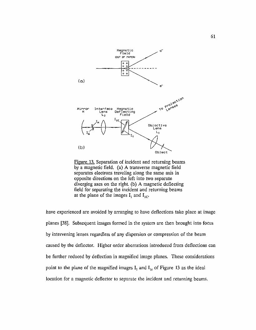
。 。
。 。
(a)
MirrorH
(b)
Magnet1 cField
(OUT OF PAPER)
Inter‘ fece Maqnet1 cLens DeFlecting
L 2 Field
11C
e
e
~'(.、。〈、
‘ ev
q(O~<aeS’‘。 、.,.0(\"0
61
Filrure 13. Separation of incident and returning beamsby a magnetic field. (a) A transverse magnetic fieldseparates electrons traveling along the sam~ axis inopposite directions on the left into two separatediverging axes on the righ t. (b) A magnetic deflectingfield for separating the incident and returning beamsat the plane of the images II and IIC'
have experienced are avoided by arranging to have deflections take place at image
planes [38]. Subsequent images formed in the system are then brought into focus
by intervening lenses regardless of any dispersion or compression of the beam
caused by the deflector. Higher order aberrations introduced from deflections can
be further reduced by deflection in magnified image planes. These considerations
point to the plane of the magnified images II and lie of Figure 13 as the ideal
location for a magnetic deflector to separate the incident and returning beams.
62
With the mirror operating in the symmetric mode, the 0피ect and image planes
coincide. The lens μ then relays the mirror’s object/image into the separating
magnet. The image in the magnet remains fixed at the center of the deflecting
field while the voltage parameters on the mirror and lens μ are adjusted together
for aberration correction of the entire lens system.
A circular cross-section for the magnetic deflecting fields is advantageous.
Since the image being transferred through the deflector occupies only a small area
near the center of the field, the beams enter and leave the deflection field
substantially at right angles to the boundary, thus avoiding the compression effects
of the fringing fields. In addition each ray heading for the center of the magnet
traverses an equal distance in the magnetic field and exits appearing to come
from the same point at the center of the field. For electrons of the same energy,
equal paths in the field produce equal an망dar deflections and results in the
absence of keystone distortion in the image common in other deflection
geometries. Since all of the rays exiting from the magnet appear to come from
the center, there is no deflection of the image position with variations of magnetic
field strength. This feature makes the image position insensitive to magnet
current and accelerating voltage power supply variations, an important
consideration in high resolution applications. Additionally, since the rays
entering the magnet cross in the center, small linear misalignment of the magnet
location is compensated by the fact that rays shortened the most entering are
shortened the least exiting, tending to make the ray paths and deflections equal.
63
This auspicious geometry appears to be particularly suitable for use with imaging
systems employing electron mirrors.
An additional concern involves the orientation of the image in the
separating field. The images II and lIe shown in Figure 13b formed by the
objective lens are not at right angles to the axes of the mirror or the projection
lenses. If the axes of the objective lens, mirror, and projection lenses can be
arranged to be parallel to each other this short-coming can be avoided. To do so
requires two deflections of the beam between the objective axis and the mirror
axis, and two deflections between the mirror axis and the projection axis, as
illustrated in Figure 6. In order for each of these deflection to take place at an
image plane, lenses are required in each leg, between the deflection fields. In
order to produce images at right angles to the mirror and projection axes, a pair
of relay lenses producing a real intermediate image is used to transfer the images
between deflectors. πIe magnification of the images on which the relay lenses
operate can be made large enough that the aberrations in the relay stages are
negligible.
Whereas a magnetic field is required for separation of the electron beams,
either magnetic or electric fields can be used for the other two deflectors. The
insensitivity of the deflector developed here to misalignment and power supply
variations has led to the incorporation of this design in all three deflection
locations of the optical system used in this study. By making the objective, mirror,
and projection axes parallel as shown in Figure 5, all three axes could be mounted
64
vertically. Vertical orientation is to be preferred in order to minimize the
sensitivity of a microscope to vibrations. The permissible levels of vibrations and
other spurious disturbances become more stringent as the resolution limit is
improved and is a serious concern in seeking to take advantage of the aberration
correction potential of the mirror. While correction of aberrations is a necessary
requirement for achieving higher resolution, it is not the only requirement, and
the correction of the primary aberrations will leave higher order effects to set the
ultimate limit to resolution.
All that can be said for the benefits of using the deflection geometry
described here for electron beams can also be said for ion beams. With the sign
of the potentials changed on the source, the lenses, the deflectors and the mirror,
the correction system performs the same function with ions as for electrons. The
only element in this system that depends upon the ratio of charge to mass is the
magnetic deflection. Here, because the deflection is small, the magnetic field can
be increased sufficiently to allow passage of ions.
APPENDIX B
DETAILS OF THE EXPERIMENT
66
This appendix contains additional details describing the equipment used in
the work reported in Chapter III and the description of the experimental
procedure employed in the study.
APPARATUS
The Gotical Bench
The experimental study was carried out in the horizontal electron optical
bench shown in the photograph in Figure 8. The optical bench consists of an
airtight cast brass enclosure mounted on a vacuum pumping station. The top of
the bench is sealed with a removable glass plate. The glass allows viewing of the
experiment in progress and aids in the initial alignment of the experiment. The
interior surface of the optical bench was lined with sheets of Mu-metal for
shielding from stray magnetic fields. The bench ordinarily contains 3 sections of a
I-meter straight V-way but was modified, replacing one of the single sections at
one end with a double V-way section. The double V-way was used to support the
optical components for the separated branches of the incident and reflected
beams for this study. The V-ways are machined to support and align the 2.125
inch diameter electron optical components used in our laboratory. The electron
source (a thermionic triode gun) and condenser lens were supported on one track,
and the objective lens and the fine-mesh assembly on the other track. A
horizontal Y-shaped block was constructed to hold the relay lenses. The interface
lens and the mirror were supported on the remaining single V-way. The magnetic
67
deflectors were located at the intersections of the relay axes with the axes of the
mirror and the condenser and objective branches. Sensitive areas of the beam
path were covered with additional mu-metal covers to further reduce the effects
of stray magnetic fields on the beam alignment. The only openings in the
magnetic shielding were those to provide electrical connections to components
and viewing access to the phosphor alignment screens. πIe required voltages and
currents were supplied to the interior of the bench through vacuum feedthroughs
at the back and at the left end of the bench. These connections were sealed with
rubber o-rings.
까Ie only s이id electrically insulating material used inside of the bench,
including the high voltage mirror and lens insulators, was Rexolite. Rexolite is a
cross-linked poly-styrene plastic having the jointly desirable features that it
possesses the highest electrical resistivity of all plastics, is mechanically rigid, and
outgasses only water vapor and carbon dioxide in vacuum.
The Power Suoolv
The accelerating voltage was supplied by a voltage regulated Computer
Power Supply Model CPS-100-N 0 to -30 kV variable source fixed at 15 kV
throughout these experiments. A schematic of the electrical supply wiring is
shown in Figure 14. The cathode, the source of electrons in the bench, was
connected directly to the high voltage source (actually the center tap of the
hairpin filament supply). A switch in the cathode circuit was used to insert one or
two 9 volt batteries in series with the cathode for chromatic aberration
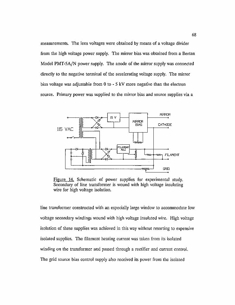
68
measurements. The lens voltages were obtained by means of a voltage divider
from the high voltage power supply. The mirror bias was obtained from a Bertan
Model PMT-5A/N power supply. The anode of the mirror supply was connected
directly to the negative terminal of the accelerating voltage supply. The mirror
bias voltage was adjustable from 0 to - 5 kV more negative than the electron
source. Primary power was supplied to the mirror bias and source supplies via a
MIRROR
MIR댄굉
BIAS I CA깨∞E
FILAMENT
GR!O
Fi!rure 14. Schematic of power supplies for experimental study.Secondary of line transformer is wound with high voltage insulatingwire for high voltage isolation.
line transformer constructed with an especially large window to accommodate low
voltage secondary windings wound with high voltage insulated wire. High voltage
isolation of these supplies was achieved in this way without resorting to expensive
isolated supplies. The filament heating current was taken from its isolated
winding on the transformer and passed through a rectifier and current control.
The grid source bias control supply also received its power from the isolated
69
transformer winding. The voltage required (300 V) was produced by a small
filament transformer wired with its low voltage winding as the primary and its
high voltage winding as the secondary. Direct current was produced with a
voltage doubler rectifier and passed to a potentiometer control on its way to the
grid.
High voltages were measured with a Keithley Model 197 Autoranging
Microvolt DMM using the Model 1600A 40 kV high voltage probe. Since the
cathode voltage was supplied from a voltage regulated source, the operating
voltage was measured when set and verified only periodically. A scale on the 10
turn mirror control knob was calibrated by measuring the mirror voltage with the
voltmeter and measurements taken from the scale thereafter.
Magnetic Deflecting Fields
All three of the magnetic deflecting fields used in these experiments were
produced by electromagnets. Each deflector consisted of a pair of coils wound on
Rexolite plac;tic forms and supported by deflection yokes constructed to confine
the deflecting field to the region of the electron beam and limit the stray
magnetic fields. Mu-metal p이e faces were adhesively attached to the pole pieces
to insure uniform magnetic fields in the gap. The pole faces were electrically
isolated from the pole pieces and wired to voltage sources to provide vertical
electrostatic deflection for beam alignment. The pair of coils for each deflector
was connected in series and each of the three deflectors was energized by an
adjustable constant current supply.
70
Lenses and Mirror
All of the lenses used in this study were electrostatic. The interface lens, used
in the mirror branch, transfers the image in the separating magnet to the mirror
and back again. The aberrations of the interface lens are thus doubled since this
lens acts on the beam travelling in both directions to and from the mirror. An
electron microscope projection lens was used in this location. The projection lens
properties were measured experimentally and are given in Table II for the range
of lens voltage ratios used.
EXPERIMENTAL PROCEDURE
The Vacuum Svstem
In order to obtain the measurements required to demonstrate the correction
of chromatic aberration of the lens system with the hyperb이ic electron mirror, the
following procedure was used. At the beginning of each experimental session the
optical bench was evacuated. The process required approximately one hour
beginning with roughing out the bench and vacuum system with the n-techanical
vacuum pump. The diffusion pump was first evacuated to about 10-2 torr where it
was valved off and the diffusion pump heater was turned on. When the pressure
in the bench reached approximately 40 x 10-3 torr, the bench and diffusion pump
were pumped in parallel. After about 20 minutes heating, the diffusion pump was
ready for use. The bench roughing line was valved off and the high vacuum valve
between the diffusion pump was slowly opened while the pressure was monitored
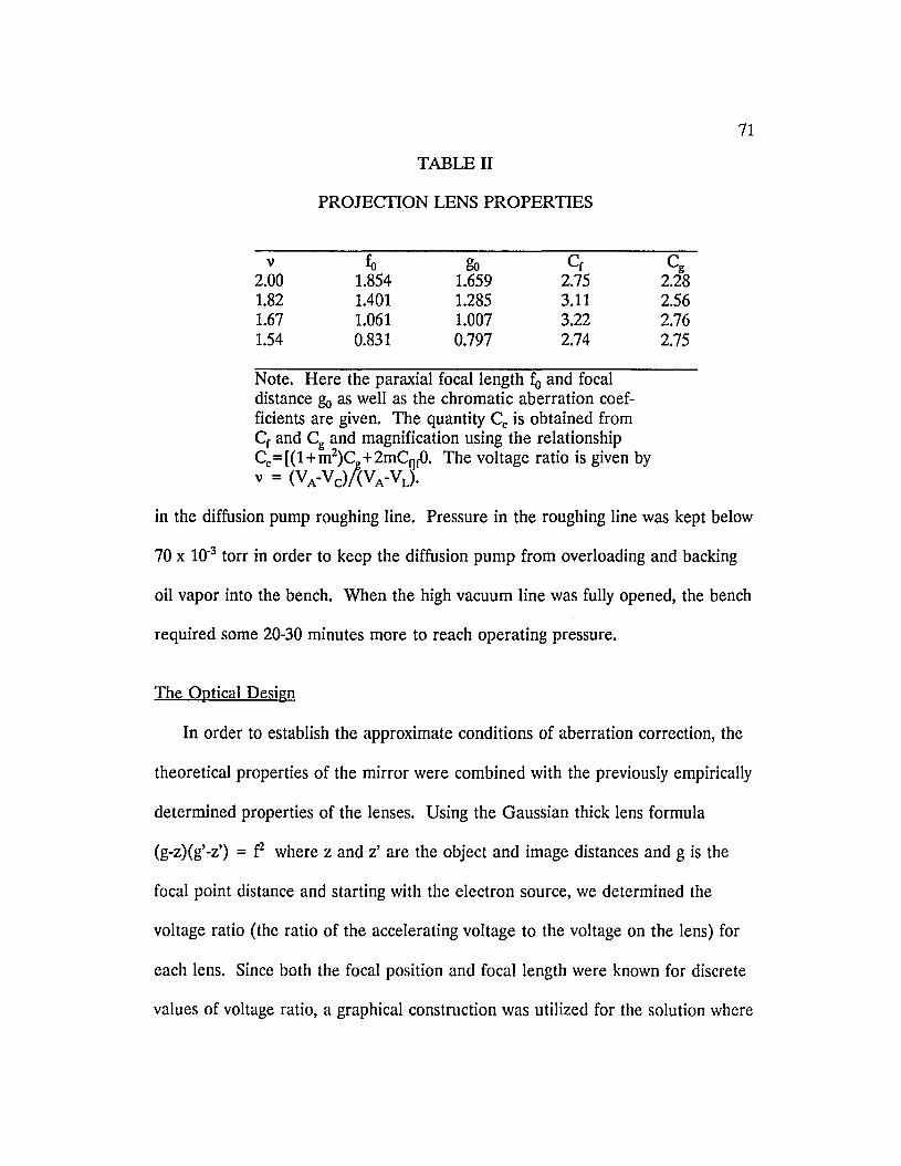
71
TABLE II
PROJECTION LENS PROPERTIES
v & g。 Cc2C2g82.00 1.854 1.659 2.75
1.82 1.401 1.285 3.11 2.561.67 1.061 1.007 3.22 2.761.54 0.831 0.797 2.74 2.75
Note. Here the paraxial focallength fa and focaldistance &> 잃 well as the chromatic aberration coefficients are given. The quantity Cc is obtained fromCcand CI! and magnification using the relationshipCc =[(1+m2)C
I!+2mCf1f0. The voltage ratio is given by
v = (VA-VdκVA-VL)·
in the diffusion pump roughing line. Pressure in the roughing line was kept below
70 X 10-3 torr in order to keep the diffusion pump from overloading and backing
oil vapor into the bench. When the high vacuum line was fully opened, the bench
required some 20-30 minutes more to reach operating pressure.
The Ootical Design
In order to establish the approximate conditions of aberration correction, the
theoretical properties of the mirror were combined with the previously empirically
determined properties of the lenses. Using the Gaussian thick lens formula
(g-z)(g’-z’) = f where z and z’ are the object and image distances and g is the
focal point distance and starting with the electron source, we determined the
voltage ratio (the ratio of the accelerating voltage to the voltage on the lens) for
each lens. Since both the focal position and focal length were known for discrete
values of voltage ratio, a graphical construction was utilized for the solution where
72
quantities f2 and (g-z)(g’-z’) were plotted against voltage ratio. The intersection
of these lines determined the expected operating point of the lens. The
experimentally determined properties of each lens were used for these
calculations.
The condenser and interface lens properties were taken from a pre띠ous study
[32]. The properties of the relay lenses were determined in a similar way at the
beginning of this study. Similarly, the objective lens properties were measured in
our optical bench for the voltage ratio = 1 used in this study.
For the calculation of the mirror location, the theoretical image location
values were used. By combining the distances between optical elements and focal
properties, voltage ratios for each lens and the mirror were determined. The
voltage divider, which consisted of twenty 20-megohm resistors connected in
series, was prepared for the experiments by replacing individual resistors with
potentiometers of equal resistance at those places where calculations indicated
taps would be necessary to operate particular lenses. The lenses and mirror were
connected to the appropriate taps with high-voltage insulated wire. The wires
were fitted with banana plugs attached to acrylic insulator rods so that voltages
could be changed while the high-voltage was on. This was a valuable asset in
locating a wayward electron beam and was useful in alignment verification.
The Alignment Procedure
With the physical locations and voltage ratios determined for the lenses and
mirror and the optical bench evacuated, the high voltage was turned on and the
73
filament current was brought up until the filament was yellow-white in color. 까le
grid voltage was advanced until light from the first phosphor alignment screen in
front of the condenser lens could be seen. Necessary adjustments to the filament
location controls were made to center the beam on the condenser screen.
Current to the first turning magnet was applied and adjusted until the beam could
be seen on the second screen on the entrance to the first relay lens. The magnet
current was adjusted to center the beam in this opening by enlarging the beam
with the condenser lens (by raising its voltage ratio along the v이tage divider
momentarily) and centering the illuminated beam around the relay lens opening.
Current was turned up in the second magnet until the beam could be found on a
screen placed just beyond this magne t. In some cases where the magnets had
been replaced or otherwise rewired, the current had to be reversed through the
magnet in order to obtain the correct deflection direction. (In some preparatory
experiments the second magnet was replaced with a phosphor screen in order to
verify the proper focussing of the relay lens pair.) The same procedure was
performed with the second magnet to center the beam in the following aperture.
At this point the beam was falling on the interface lens. As the current in the
second magnet was adjusted to sweep the beam across the interface lens opening,
the beam could be seen to sweep across the screen in front of the mirror. The
beam was centered on the opening to the mirror. The mirror voltage was brought
up slowly and a beam could be seen on the following screen placed at the rear of
the interface lens (mirror side). (Here or earlier the filament grid bias was
74
adjusted for the peak illumination on one of these intermediate phosphor screens
and the filament current adjusted for adequate brightness.) ’The beam was thus
traced back to the second magnet. Adjustment of the mirror or interface voltage
revealed the centering of the beam on the entrance to the second relay lens pair.
At this point the symmetry of the three intersecting axes determined the beam
alignment. Some exercise was required to mechanically align these three axes.
Mechanical repositioning of the relay lens assembly with metal shims was tried
until satisfactory alignment was obtained. Since the electrostatic deflectors in the
magnets were in image planes for the beam, little or no displacement of the beam
was found for these controls and the alignment of the second relay lens pair had
to be done mechanically. A number of electrostatic and magnetic alignment
fixtures were designed, constructed and tested in order to alleviate this problem.
The final results were obtained with a combination of mechanical alignment and a
small lateral voltage applied to the second magnet where the pole faces had been
divided in two along the mirror axis.
During most of the investigations where sufficient room was allotted between
the third magnet and the objective lens, a small phosphor screen could be swung
into the beam with one of the mechanical manipulators. Investigation of the
beam at this location disclosed the characteristic caustic of the beam according to
the magnitude and sign of the spherical aberration present. This was particularly
useful in verifying the predicted behavior of the mirror and the functional
relationship of the correction formulas developed here. (As an aside, the
75
behavior of the caustic on this screen stimulated reproducing this behavior with
light optics and resulted in two additional papers [33,39] and a new geometrical
theory of resolution.) Initially it was hoped that spherical aberration could be
corrected simultaneously with chromatic aberration. Observations of the beam
incident on the objective lens vindicated predictions of this possibility but
coarseness in the beam alignment capabilities of the experimental apparatus
precluded achieving our best results of simultaneous correction. As the beam
could be observed prior and following the objective lens, the beam could be seen
to go from overcorrected to undercorrected behavior under the influence of the
objective lens alone, further reinforcing our predictions.
EXPERIMENTAL RESULTS
Once the beam was satisfactorily aligned in the bench and the lenses were set
to the expected voltages, the mirror voltage was brought up until illumination
could be seen on the final screen. The location of a lOOO/inch mesh was varied
along the axis until a high magnification shadow of the mesh could be seen on the
output screen. By translating the mesh along the axis of the beam, its location
with respect to the caustic could easily be found. The magnification would
gradually grow as the mesh moved toward the caustic, the mesh bars disappearing
altogether as the whole beam passed through one opening in the mesh(!), and
reappearing on the other side gradually growing smaller as the mesh retreated
from the caustic. Distortion patterns associated with the magnitude and sign of
76
the spherical aberration could also be seen as the mesh was translated along the
beam. (Pincushion distortion for the mesh between the lens and caustic with
ordinary undercorrected spherical aberration and barrel distortion for
overcorrected spherical a,berration. IThe distortion types are reversed for the
mesh positioned beyond the caustic,.)
Chromatic aberra~jon was studied by observing change in the shadow
magnification with incremental changes in the electron beam accelerating voltage.
For example, with the m~sh positioned beyond the final image, if an increase in
beam voltage was accompanied by an increase in magnification, this indicated that
the image had moved toward the mesh and away from the lens, and that the
chromatic aberration Was undercorrected. A decrease in magnification for the
same change in voltage would indicate over-correction.
When the optical arflll1gement was such that illumination on the final screen
was too dim to view satisfactorily, aln image intensifier was used to increase
illumination. The intensified shadow patterns could be imaged with a CCD video
camera and viewed on a monitor. These patterns were recorded on a video
cassette recorder. Result.s were photographed off of the monitor with a 35-mm
camera and measuremenis made on prints from these pictures. Calibration of the
final image size was acconIplished by ratioing the measurements of the mesh on
the final photograph to the image intensifier diameter on the photograph. The
diameter of the image in(:ensifier output screen was 1.125 inches.