Embed Size (px)
Citation preview
UC Regents Fall 2005 © UCBCS 152 L11: VLSI
2005-10-6John Lazzaro
(www.cs.berkeley.edu/~lazzaro)
CS 152 Computer Architecture and Engineering
Lecture 11 – VLSI
www-inst.eecs.berkeley.edu/~cs152/
TAs: David Marquardt and Udam Saini
UC Regents Fall 2005 © UCBCS 152 L11: VLSI
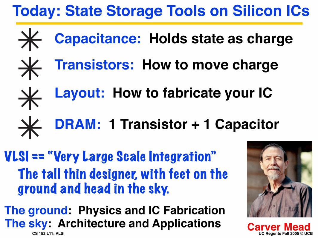
Today: State Storage Tools on Silicon ICsCapacitance: Holds state as charge
Transistors: How to move charge
VLSI == “Very Large Scale Integration”The tall thin designer, with feet on the ground and head in the sky.
Carver Mead The ground: Physics and IC FabricationThe sky: Architecture and Applications
Layout: How to fabricate your IC
DRAM: 1 Transistor + 1 Capacitor
UC Regents Fall 2005 © UCBCS 152 L11: VLSI
Capacitance
UC Regents Fall 2005 © UCBCS 152 L11: VLSI
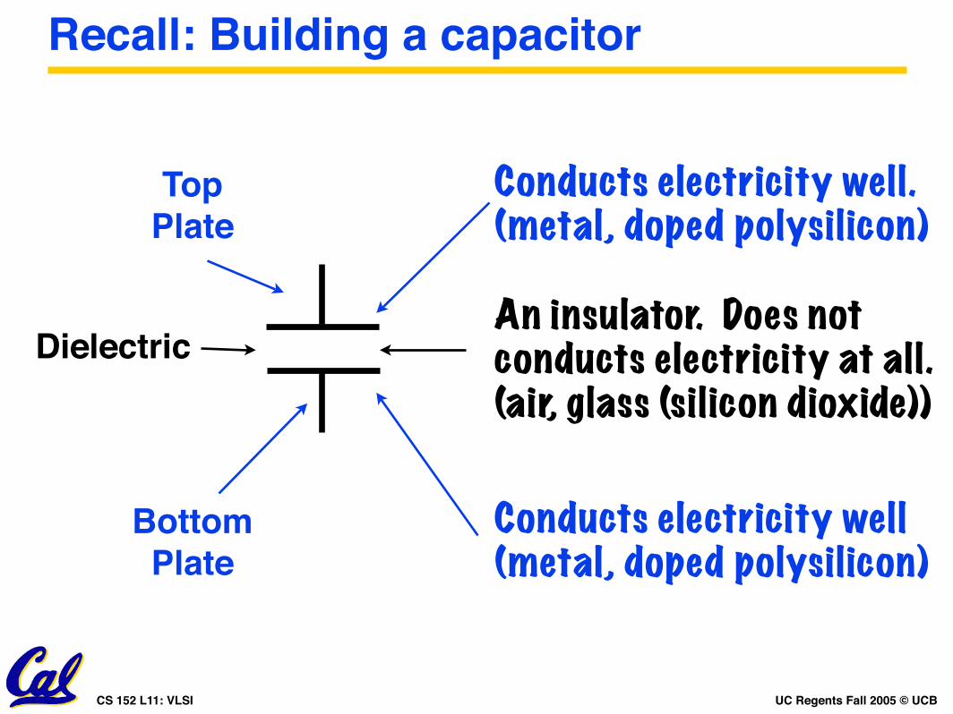
Recall: Building a capacitor
Conducts electricity well.(metal, doped polysilicon)
TopPlate
BottomPlate
Conducts electricity well(metal, doped polysilicon)
DielectricAn insulator. Does not conducts electricity at all.(air, glass (silicon dioxide))
UC Regents Fall 2005 © UCBCS 152 L11: VLSI
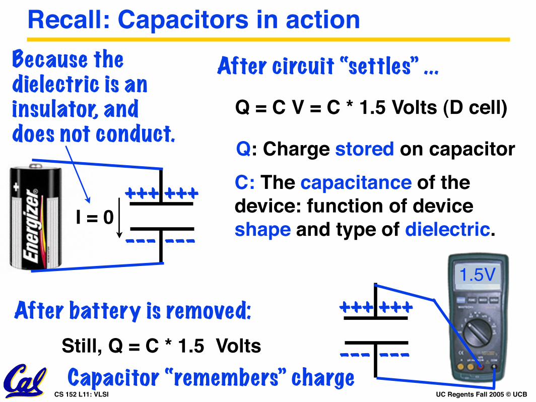
Recall: Capacitors in action
I = 0
Because the dielectric is an insulator, and does not conduct.
After circuit “settles” ...
Q = C V = C * 1.5 Volts (D cell)
Q: Charge stored on capacitorC: The capacitance of the device: function of device shape and type of dielectric.
+++ +++
--- ---
After battery is removed: +++ +++
--- ---Still, Q = C * 1.5 VoltsCapacitor “remembers” charge
1.5V

UC Regents Fall 2005 © UCBCS 152 L11: VLSI
Capacitors and current ...Q = C V
+++ +++
--- ---I V
Differentiate with respect to time ... if C != C(t) ...
dQ/dt = C dV/dt
Observation: If a voltage change dV occurs in zero time (dt = 0), the current I is infinite (impossible).
The voltage across a capacitor cannot change instantaneously. And by Q = C V, the charge stored
on a capacitor cannot change instantaneously.
I is defined as dQ/dt ...
I = C dV/dt
UC Regents Fall 2005 © UCBCS 152 L11: VLSI
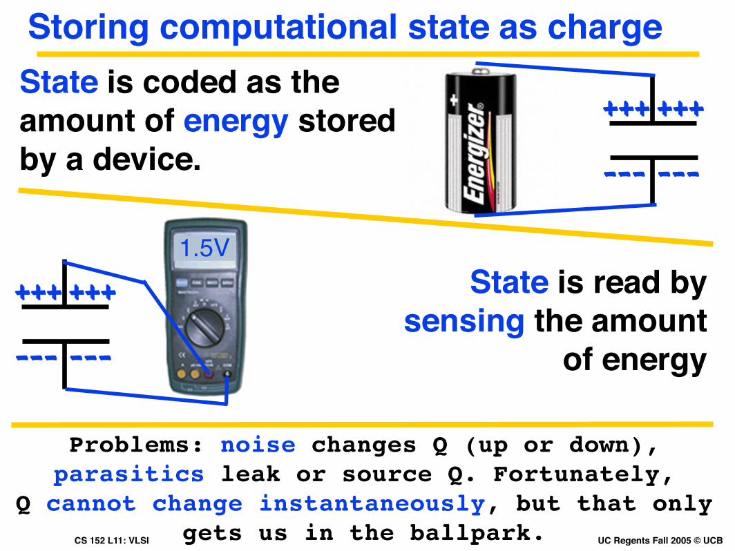
State is coded as the amount of energy stored by a device.
+++ +++
--- ---
Storing computational state as charge
State is read by sensing the amount
of energy
+++ +++
--- ---
1.5V
Problems: noise changes Q (up or down), parasitics leak or source Q. Fortunately,
Q cannot change instantaneously, but that only gets us in the ballpark.

UC Regents Fall 2005 © UCBCS 152 L11: VLSI
How do we fight noise and win?Store more energy than we expect from the noise.
Q = CV. To store more charge, use a bigger V or
make a bigger C.Cost: Power, chip size.
Example: 1 bit per capacitor.Write 1.5 volts on C.
To read C, measure V.V > 0.75 volts is a “1”.V < 0.75 volts is a “0”.
Cost: Could have stored many bits on that capacitor.
Represent stateas charge in ways that are robust to noise.
Correct small state errors that are introduced by noise.
Ex: read C every 1 msIs V > 0.75 volts?Write back 1.5V (yes) or 0V (no).Cost: Complexity.
UC Regents Fall 2005 © UCBCS 152 L11: VLSI
MOS Transistors
Two diodes and a capacitor in an interesting arrangement. So, we begin with a diode review ...
UC Regents Fall 2005 © UCBCS 152 L11: VLSI
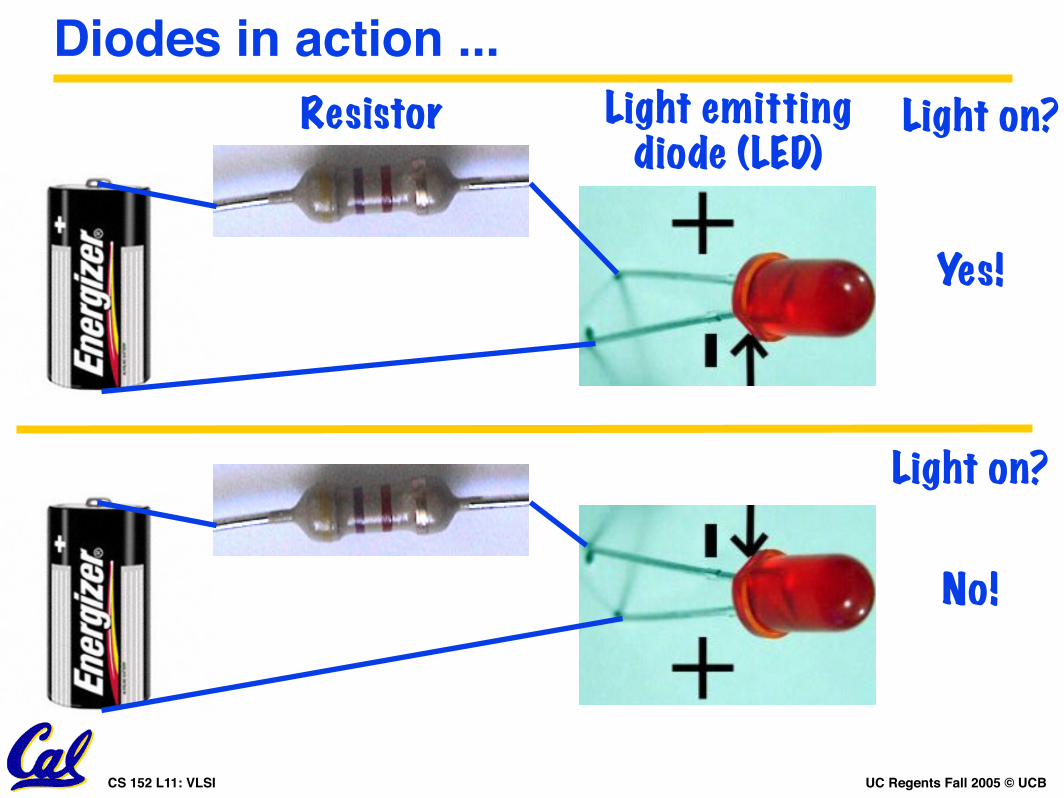
Diodes in action ...Light emitting
diode (LED)Resistor Light on?
Yes!
No!
Light on?
UC Regents Fall 2005 © UCBCS 152 L11: VLSI
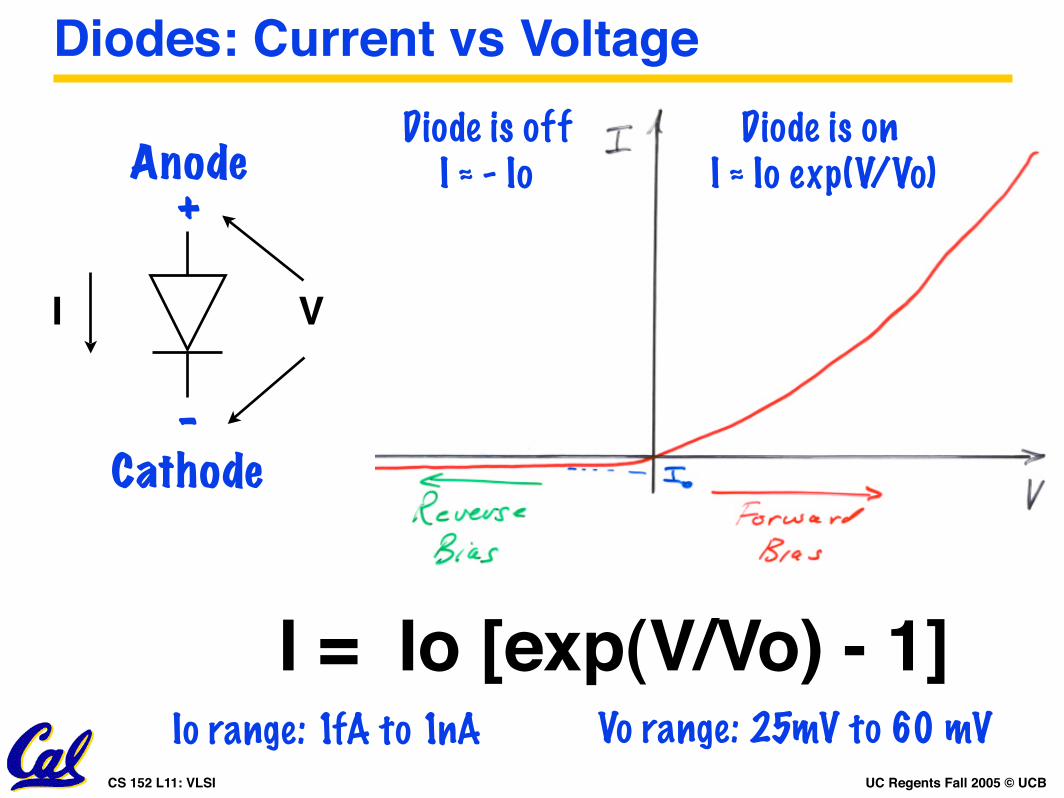
Diodes: Current vs Voltage
Anode+
-Cathode
I V
Diode is onI ⋲ Io exp(V/Vo)
I = Io [exp(V/Vo) - 1]Io range: 1fA to 1nA Vo range: 25mV to 60 mV
Diode is offI ⋲ - Io
UC Regents Fall 2005 © UCBCS 152 L11: VLSI
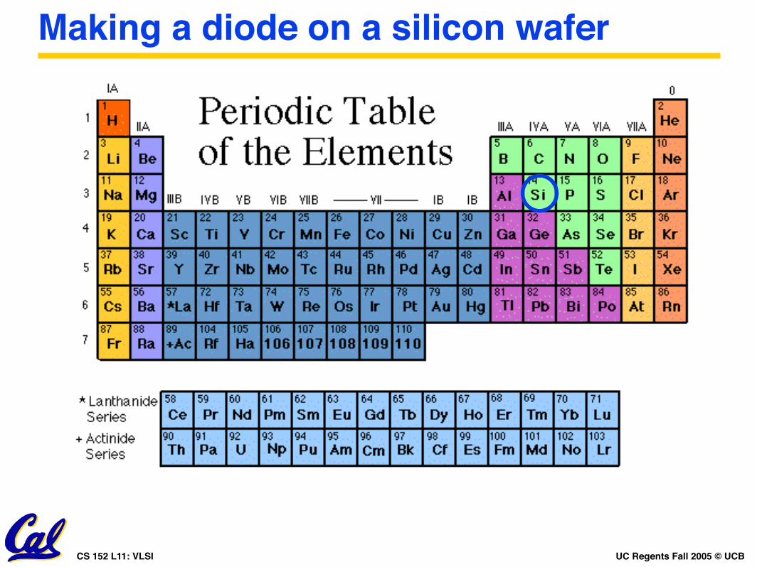
Making a diode on a silicon wafer
UC Regents Fall 2005 © UCBCS 152 L11: VLSI
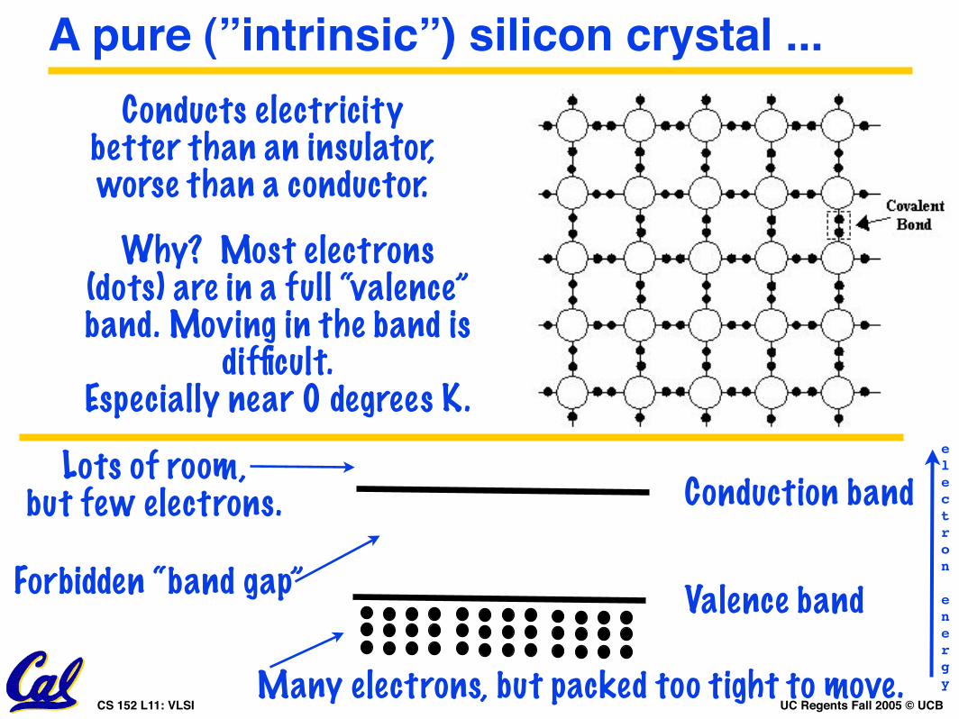
A pure (”intrinsic”) silicon crystal ...Conducts electricity
better than an insulator, worse than a conductor.
Why? Most electrons (dots) are in a full “valence” band. Moving in the band is
difficult.Especially near 0 degrees K.
Many electrons, but packed too tight to move.
Lots of room, but few electrons.
electron
energy
Valence band
Conduction band
Forbidden “band gap”
UC Regents Fall 2005 © UCBCS 152 L11: VLSI
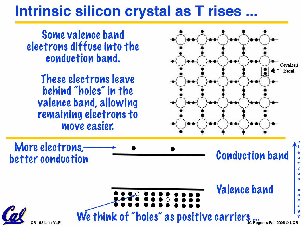
Intrinsic silicon crystal as T rises ...Some valence band
electrons diffuse into the conduction band.
These electrons leave behind “holes” in the
valence band, allowing remaining electrons to
move easier.
We think of “holes” as positive carriers ...
More electrons,better conduction
Valence band
Conduction band
electron
energy
UC Regents Fall 2005 © UCBCS 152 L11: VLSI
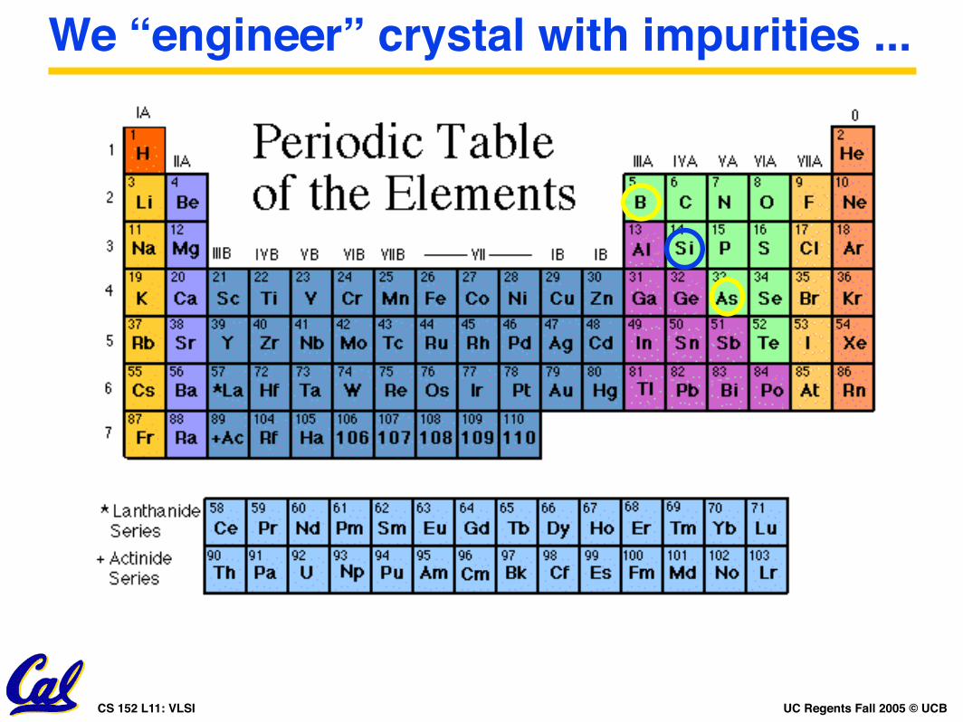
We “engineer” crystal with impurities ...

UC Regents Fall 2005 © UCBCS 152 L11: VLSI
N-type silicon: add donor atoms
Use diffusion or ion implantation to replace some
of the Si atoms with As
Arsensic has an extra electron that is “donates” to
the conduction band.
Valence band
Conduction bandelectron
energy
Electronsfrom donor atoms.
Improves conductivy.
Donor energy
No change in the number of holes
n+ : heavy doping. n- : light doping.
UC Regents Fall 2005 © UCBCS 152 L11: VLSI
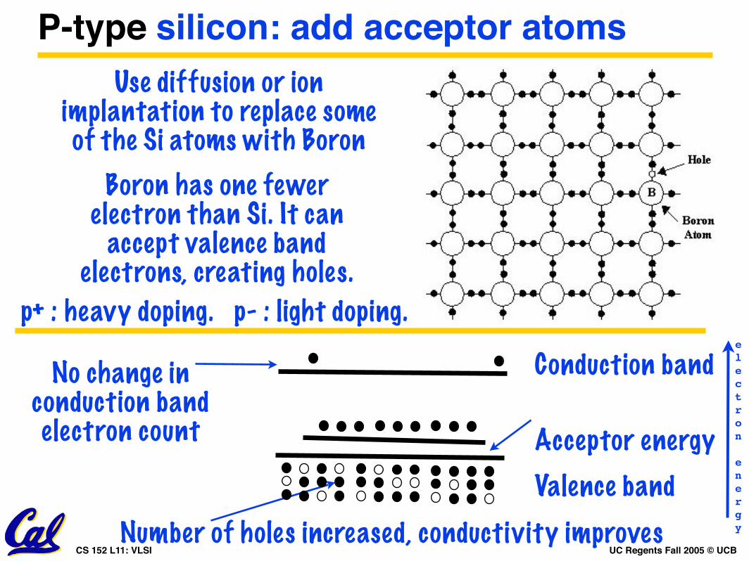
P-type silicon: add acceptor atomsUse diffusion or ion
implantation to replace some of the Si atoms with Boron
Boron has one fewer electron than Si. It can
accept valence band electrons, creating holes.
No change in conduction band electron count Acceptor energy
Number of holes increased, conductivity improves
Valence band
Conduction bandelectron
energy
p+ : heavy doping. p- : light doping.
UC Regents Fall 2005 © UCBCS 152 L11: VLSI
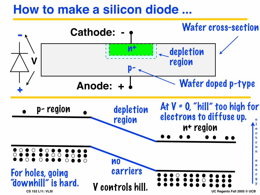
How to make a silicon diode ...Wafer cross-section
n+
p-
Wafer doped p-type
n+ region
p- region At V = 0, “hill” too high for electrons to diffuse up.
V
Cathode: -
+
-
Anode: +
no carriers
depletion region
For holes, going “downhill” is hard. V controls hill.
electron
energy
depletion region

UC Regents Fall 2005 © UCBCS 152 L11: VLSI
Diodes: Current vs Voltage
Anode+
-Cathode
I V
Diode is onI ⋲ Io exp(V/Vo)
I = Io [exp(V/Vo) - 1]Io range: 1fA to 1nA Vo range: 25mV to 60 mV
Diode is offI ⋲ - Io

UC Regents Fall 2005 © UCBCS 152 L11: VLSI
Note: IC Diodes are biased “off”!
p-
n+
V1
0 V - “ground”
n+
V2V1 V2
V1, V2 > 0V. Diodes “off”, only current is Io “leakage”.
I = Io [exp(V/Vo) - 1]Anodes of all diodes on wafer connected to ground.
UC Regents Fall 2005 © UCBCS 152 L11: VLSI
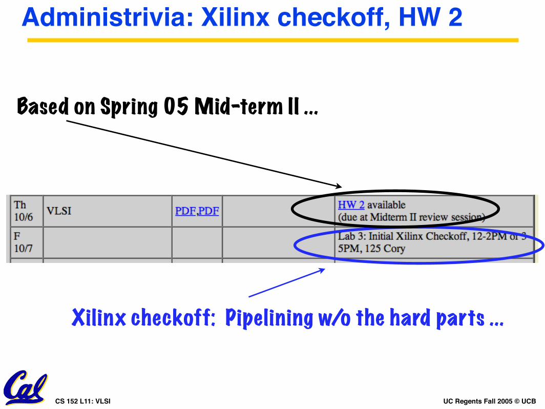
Administrivia: Xilinx checkoff, HW 2
Based on Spring 05 Mid-term II ...
Xilinx checkoff: Pipelining w/o the hard parts ...
UC Regents Fall 2005 © UCBCS 152 L11: VLSI
MOS Transistors
Two diodes and a capacitor in an interesting arrangement ...

UC Regents Fall 2005 © UCBCS 152 L11: VLSI
What we want: the perfect switch.
p-
n+
V1
n+
V2Switch is off. V1 is not
connected to V2.
p-
V1
n+
V2Switch is on. V1 is connected
to V2.
We want to turn a p-type region into an n-type region under
voltage control.
We need electrons to fill valence holes and add
conduction band electrons
+++ +++
--- ---
UC Regents Fall 2005 © UCBCS 152 L11: VLSI
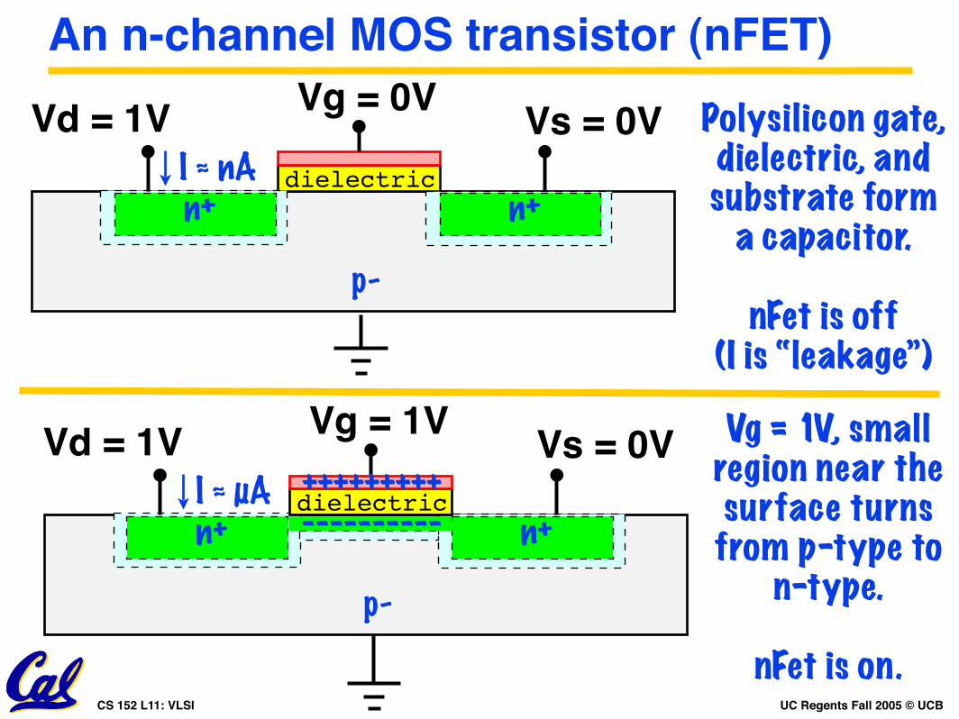
An n-channel MOS transistor (nFET)
p-
n+
Vd = 1V
n+
Vs = 0V Polysilicon gate,dielectric, and substrate form
a capacitor.
nFet is off(I is “leakage”)
dielectric
Vg = 0VI ⋲ nA
----------
p-
n+
Vd = 1V
n+
Vs = 0Vdielectric
Vg = 1V+++++++++----------
Vg = 1V, small region near the surface turns
from p-type to n-type.
nFet is on.
I ⋲ µA
UC Regents Fall 2005 © UCBCS 152 L11: VLSI
Drawing an nFET
“Mask” drawings sent to the fabrication facility to make the chips.
UC Regents Fall 2005 © UCBCS 152 L11: VLSI
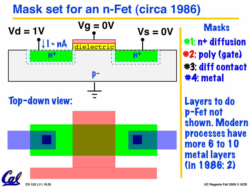
Mask set for an n-Fet (circa 1986)
p-
n+
Vd = 1V
n+
Vs = 0Vdielectric
Vg = 0VI ⋲ nA #1: n+ diffusion
Top-down view:
Masks
#3: diff contact#2: poly (gate)
#4: metal
Layers to do p-Fet not shown. Modern processes have more 6 to 10 metal layers(in 1986: 2)
UC Regents Fall 2005 © UCBCS 152 L11: VLSI
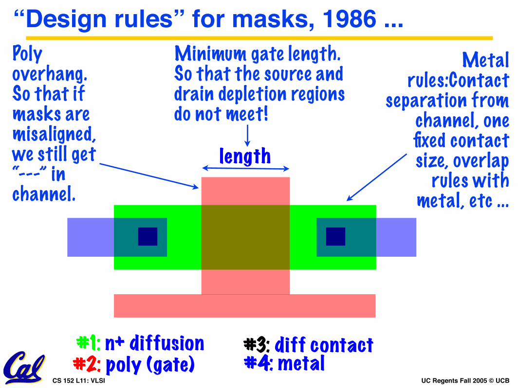
“Design rules” for masks, 1986 ...
#1: n+ diffusion #3: diff contact#2: poly (gate) #4: metal
Poly overhang. So that if masks are misaligned, we still get “---” in channel.
Minimum gate length. So that the source and drain depletion regions do not meet!
length
Metal rules:Contact
separation from channel, one fixed contact size, overlap
rules with metal, etc ...
UC Regents Fall 2005 © UCBCS 152 L11: VLSI
Fabrication

UC Regents Fall 2005 © UCBCS 152 L11: VLSI
Mask set for an n-Fet ...
p-
n+
Vd = 1V
n+
Vs = 0Vdielectric
Vg = 1V
#1: n+ diffusionTop-down view:
Masks
#3: diff contact#2: poly (gate)
#4: metal
How does a fab use a mask set to make an IC?
Vg
Vd
Vs
Ids I ⋲ µA

UC Regents Fall 2005 © UCBCS 152 L11: VLSI
Start with an un-doped wafer ...
Steps
p-
#1: dope wafer p-
#5: place positive poly mask and expose with UV.
UV hardens exposed resist. A wafer wash leaves only hard resist.
#2: grow gate oxide
oxide
#3: grow undoped polysilicon
#4: spin on photoresist
UC Regents Fall 2005 © UCBCS 152 L11: VLSI
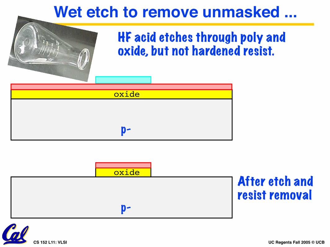
Wet etch to remove unmasked ...
p-
oxide
HF acid etches through poly and oxide, but not hardened resist.
p-
oxideAfter etch and resist removal
UC Regents Fall 2005 © UCBCS 152 L11: VLSI
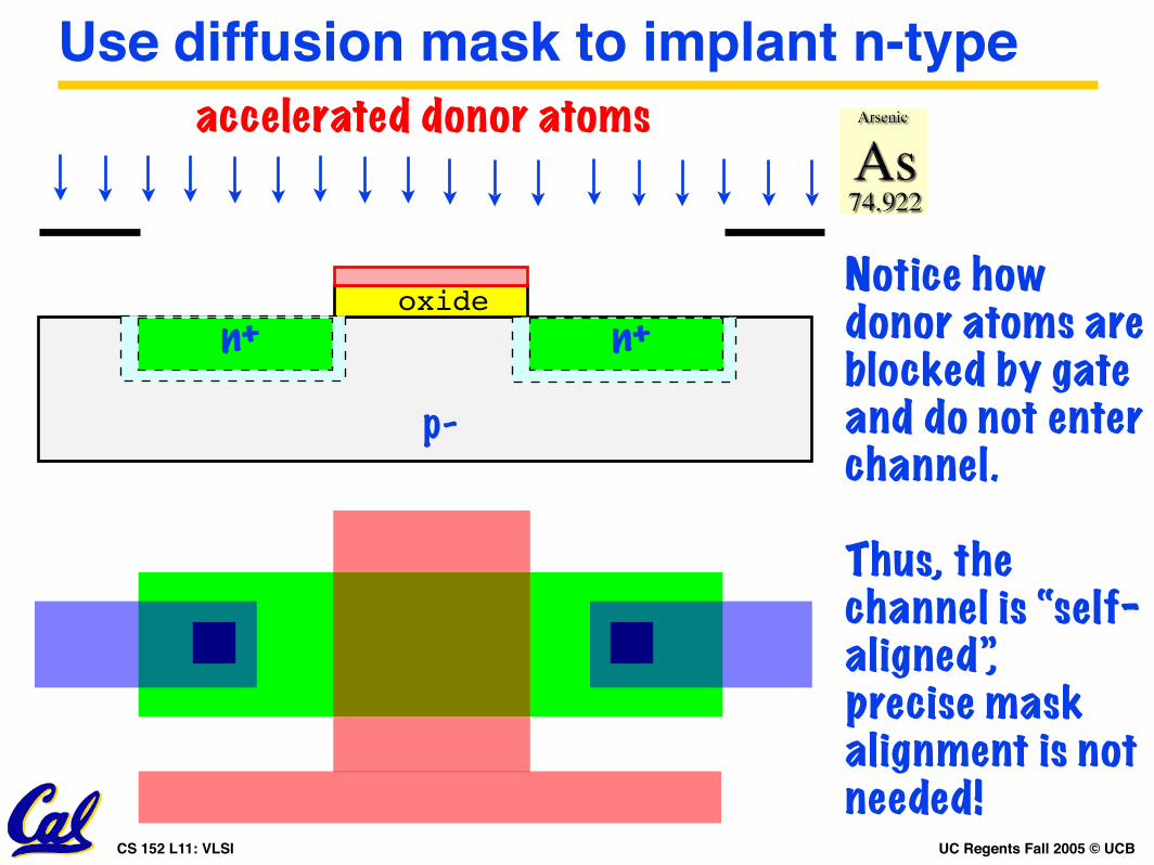
Use diffusion mask to implant n-type
p-
oxide
accelerated donor atoms
n+ n+
Notice how donor atoms are blocked by gate and do not enter channel.
Thus, the channel is “self-aligned”,precise mask alignment is not needed!
UC Regents Fall 2005 © UCBCS 152 L11: VLSI
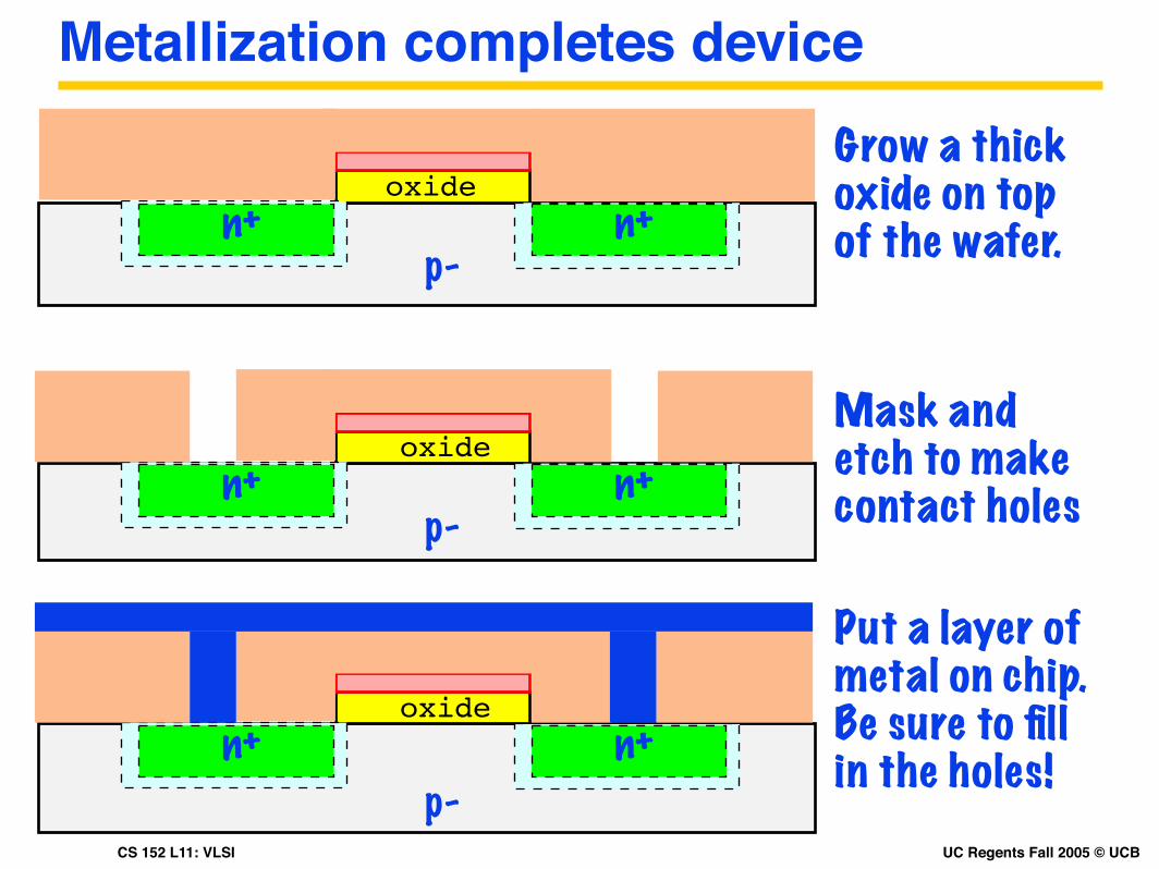
Metallization completes device
p-
oxiden+ n+
Grow a thick oxide on topof the wafer.
p-
oxiden+ n+
Mask and etch to make contact holes
p-
oxiden+ n+
Put a layer of metal on chip.Be sure to fill in the holes!
UC Regents Fall 2005 © UCBCS 152 L11: VLSI
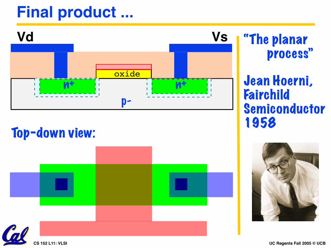
Final product ...
Top-down view:
p-
oxiden+ n+
Vd Vs “The planar process”
Jean Hoerni,Fairchild Semiconductor1958
UC Regents Fall 2005 © UCBCS 152 L11: VLSI
p-channel Transistors
UC Regents Fall 2005 © UCBCS 152 L11: VLSI
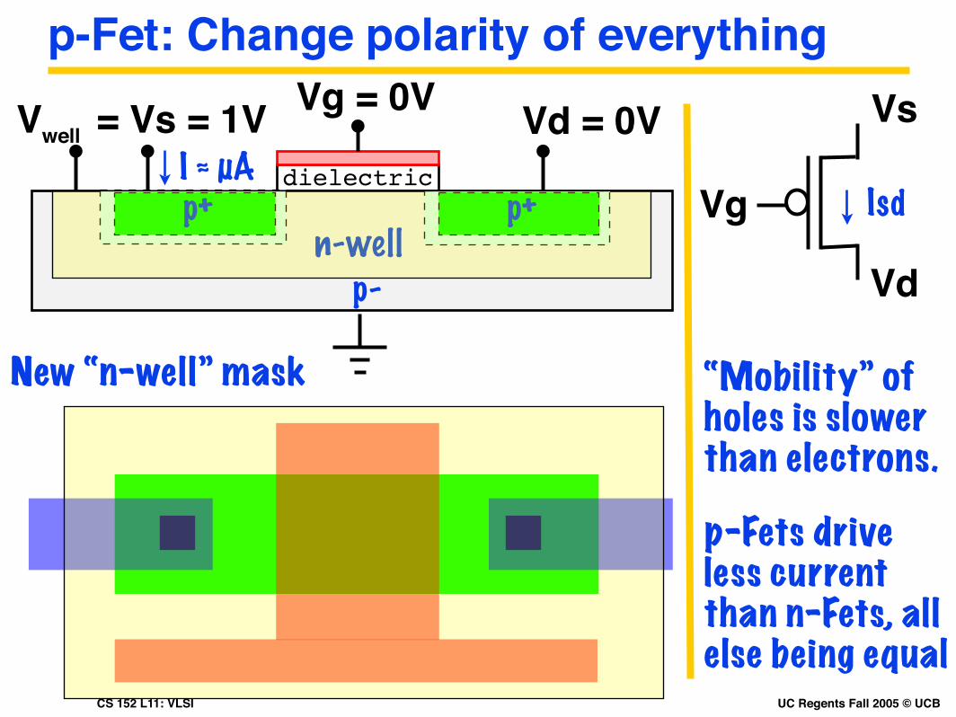
p-Fet: Change polarity of everything
n-wellp+
Vwell = Vs = 1V
p+
Vd = 0Vdielectric
Vg = 0VI ⋲ µA
p-
New “n-well” mask
Vg
Vs
Vd
Isd
“Mobility” of holes is slowerthan electrons.
p-Fets drive less current than n-Fets, all else being equal
UC Regents Fall 2005 © UCBCS 152 L11: VLSI
Device Equations
UC Regents Fall 2005 © UCBCS 152 L11: VLSI
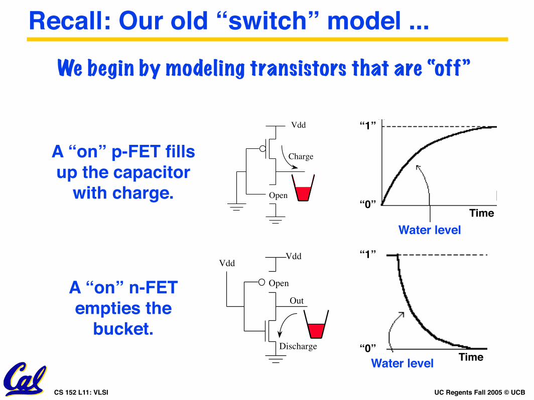
Recall: Our old “switch” model ...
A “on” p-FET fillsup the capacitor
with charge.
1/28/04 ©UCB Spring 2004CS152 / Kubiatowicz
Lec3.29
Delay Model:
CMOS
1/28/04 ©UCB Spring 2004CS152 / Kubiatowicz
Lec3.30
Review: General C/L Cell Delay Model
° Combinational Cell (symbol) is fully specified by:• functional (input -> output) behavior
- truth-table, logic equation, VHDL
• load factor of each input
• critical propagation delay from each input to each output for each transition
- THL(A, o) = Fixed Internal Delay + Load-dependent-delay x load
° Linear model composes
Cout
Vout
Cout
Delay
Va -> Vout
XX
X
X
X
X
Ccritical
delay per unit load
A
B
X
.
.
.
Combinational
Logic Cell
Internal Delay
1/28/04 ©UCB Spring 2004CS152 / Kubiatowicz
Lec3.31
Basic Technology: CMOS
° CMOS: Complementary Metal Oxide Semiconductor• NMOS (N-Type Metal Oxide Semiconductor) transistors
• PMOS (P-Type Metal Oxide Semiconductor) transistors
° NMOS Transistor• Apply a HIGH (Vdd) to its gate
turns the transistor into a “conductor”
• Apply a LOW (GND) to its gateshuts off the conduction path
° PMOS Transistor• Apply a HIGH (Vdd) to its gate
shuts off the conduction path
• Apply a LOW (GND) to its gateturns the transistor into a “conductor”
Vdd = 5V
GND = 0v
Vdd = 5V
GND = 0v
1/28/04 ©UCB Spring 2004CS152 / Kubiatowicz
Lec3.32
Basic Components: CMOS Inverter
Vdd
Circuit
° Inverter Operation
OutIn
SymbolPMOS
NMOS
In Out
Vdd
Open
Charge
VoutVdd
Vdd
Out
Open
Discharge
Vin
Vdd
Vdd
A “on” n-FET empties the
bucket.
1/28/04 ©UCB Spring 2004CS152 / Kubiatowicz
Lec3.29
Delay Model:
CMOS
1/28/04 ©UCB Spring 2004CS152 / Kubiatowicz
Lec3.30
Review: General C/L Cell Delay Model
° Combinational Cell (symbol) is fully specified by:• functional (input -> output) behavior
- truth-table, logic equation, VHDL
• load factor of each input
• critical propagation delay from each input to each output for each transition
- THL(A, o) = Fixed Internal Delay + Load-dependent-delay x load
° Linear model composes
Cout
Vout
Cout
Delay
Va -> Vout
XX
X
X
X
X
Ccritical
delay per unit load
A
B
X
.
.
.
Combinational
Logic Cell
Internal Delay
1/28/04 ©UCB Spring 2004CS152 / Kubiatowicz
Lec3.31
Basic Technology: CMOS
° CMOS: Complementary Metal Oxide Semiconductor• NMOS (N-Type Metal Oxide Semiconductor) transistors
• PMOS (P-Type Metal Oxide Semiconductor) transistors
° NMOS Transistor• Apply a HIGH (Vdd) to its gate
turns the transistor into a “conductor”
• Apply a LOW (GND) to its gateshuts off the conduction path
° PMOS Transistor• Apply a HIGH (Vdd) to its gate
shuts off the conduction path
• Apply a LOW (GND) to its gateturns the transistor into a “conductor”
Vdd = 5V
GND = 0v
Vdd = 5V
GND = 0v
1/28/04 ©UCB Spring 2004CS152 / Kubiatowicz
Lec3.32
Basic Components: CMOS Inverter
Vdd
Circuit
° Inverter Operation
OutIn
SymbolPMOS
NMOS
In Out
Vdd
Open
Charge
VoutVdd
Vdd
Out
Open
Discharge
Vin
Vdd
Vdd
!"#$%&'())* ++,!-.)'/ 012-)34$5$%& 67&1'-)
!"#$%&'(#)*(+,%-$*".(/0
1 2+.$0#$03
1 4546%,"#$3
“1”
“0”Time
Water level
!"#$%&'())* ++,!-.)'/ 012-)34$5$%& 67&1'-)
!"#$%&'(#)*(+,%-$*".(/0
1 2+.$0#$03
1 4546%,"#$3
“0”
“1”
TimeWater level
We begin by modeling transistors that are “off”
UC Regents Fall 2005 © UCBCS 152 L11: VLSI
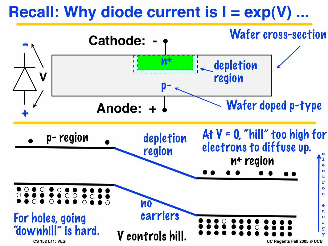
Recall: Why diode current is I = exp(V) ...Wafer cross-section
n+
p-
Wafer doped p-type
n+ region
p- region At V = 0, “hill” too high for electrons to diffuse up.
V
Cathode: -
+
-
Anode: +
no carriers
depletion region
For holes, going “downhill” is hard. V controls hill.
electron
energy
depletion region
UC Regents Fall 2005 © UCBCS 152 L11: VLSI
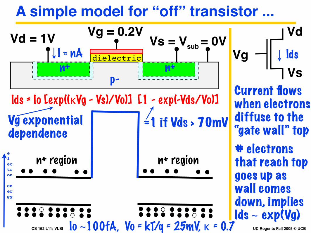
A simple model for “off” transistor ...
p-n+
Vd = 1V
n+
Vs = Vsub = 0Vdielectric
Vg = 0.2V
Vg
Vd
VsIds I ⋲ nA
n+ regionelectron
energy
n+ region
Current flows when electrons diffuse to the “gate wall” top
# electrons that reach top goes up as wall comesdown, implies Ids ~ exp(Vg)
Ids = Io [exp((κVg - Vs)/Vo)] [1 - exp(-Vds/Vo)]
Io ~100fA, Vo = kT/q = 25mV, κ = 0.7
Vg exponential dependence
⋲1 if Vds > 70mV

UC Regents Fall 2005 © UCBCS 152 L11: VLSI
----------
p-n+
Vd = 2V
n+dielectric
Vg = 1V+++++++++----------
A simple model for “on” transistor ...
Vs = Vsub = 0VI ⋲ µA Vg
Vd
VsIds
Ids = (carriers in channel) / (transit time)Q = CV f(length, velocity)
Ids = [(µεW)/(LD)] [Vgs -Vth] [Vds]
If Vds > Vgs - Vth, channel physics change :
Ids = [(µεW)/(2LD)] [Vgs -Vth]^2 W = transistor width, L = length,
D = capacitor plate distance µ is velocity, ε is C dilectric constant
UC Regents Fall 2005 © UCBCS 152 L11: VLSI
Dynamic Memory (DRAM)

UC Regents Fall 2005 © UCBCS 152 L11: VLSI
Recall: Capacitors in action
I = 0
Because the dielectric is an insulator, and does not conduct.
After circuit “settles” ...
Q = C V = C * 1.5 Volts (D cell)
Q: Charge stored on capacitorC: The capacitance of the device: function of device shape and type of dielectric.
+++ +++
--- ---
After battery is removed: +++ +++
--- ---Still, Q = C * 1.5 VoltsCapacitor “remembers” charge
1.5V

UC Regents Fall 2005 © UCBCS 152 L11: VLSI
DRAM cell: 1 transistor, 1 capacitor
Vdd
Capacitor
“Word Line”“Bit Line”
p-
oxiden+ n+
oxide------
“Bit Line”
Word Line and Vdd run on “z-axis”
Word Line
Vdd
“Bit Line”
Vdd
Diode leakagecurrent.
Why Vcap values start out at ground.
Vcap
UC Regents Fall 2005 © UCBCS 152 L11: VLSI
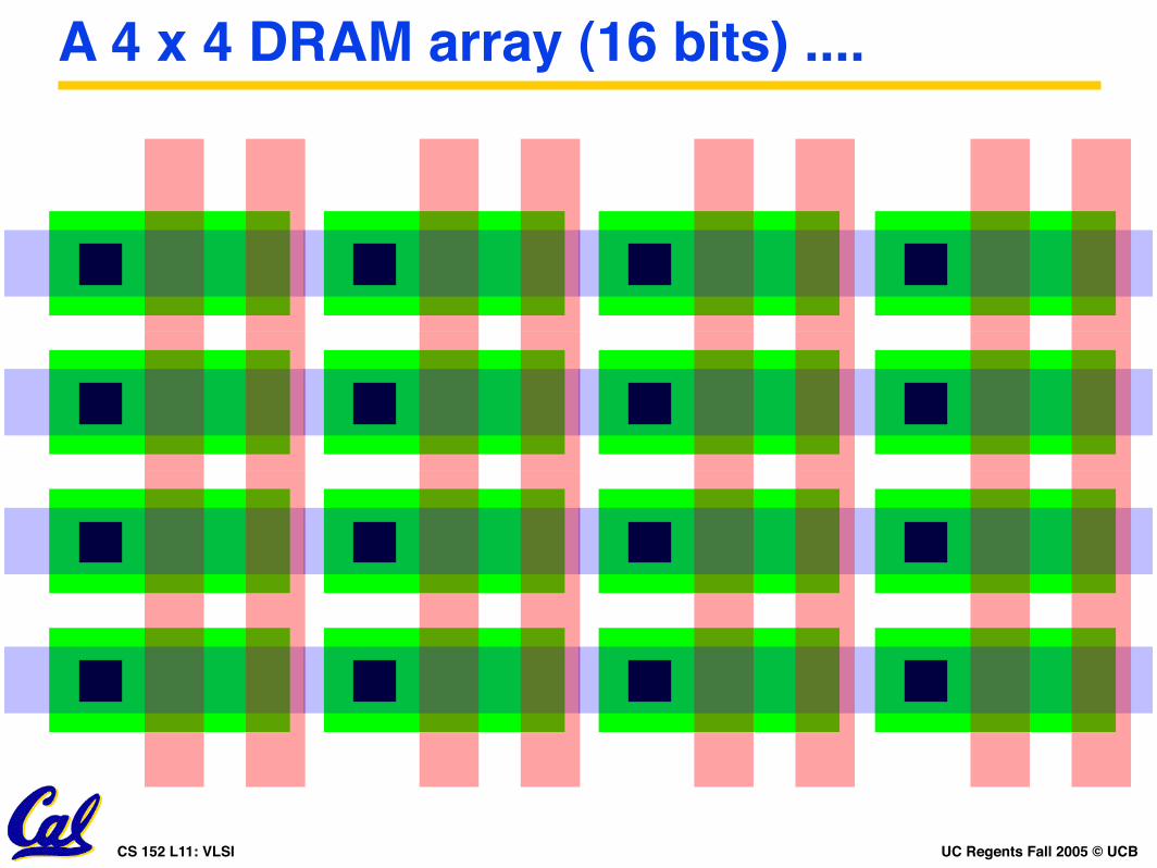
A 4 x 4 DRAM array (16 bits) ....
UC Regents Fall 2005 © UCBCS 152 L11: VLSI
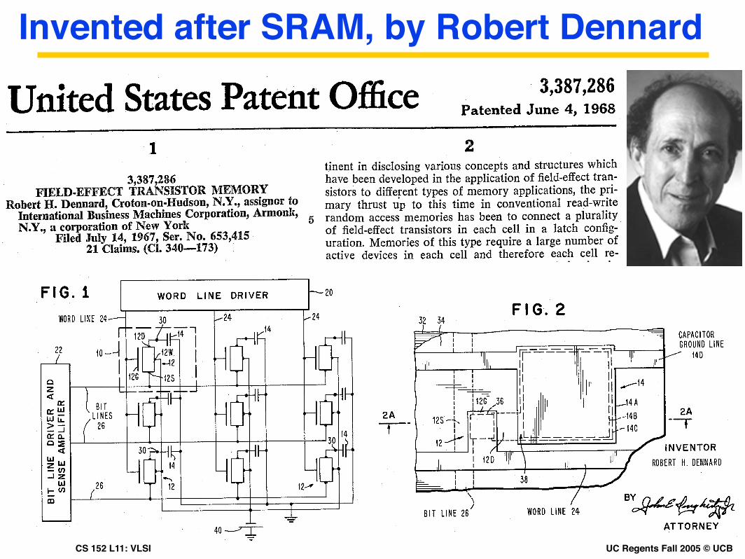
Invented after SRAM, by Robert Dennard
www.FreePatentsOnline.com
www.FreePatentsOnline.com
www.FreePatentsOnline.com
UC Regents Fall 2005 © UCBCS 152 L11: VLSI
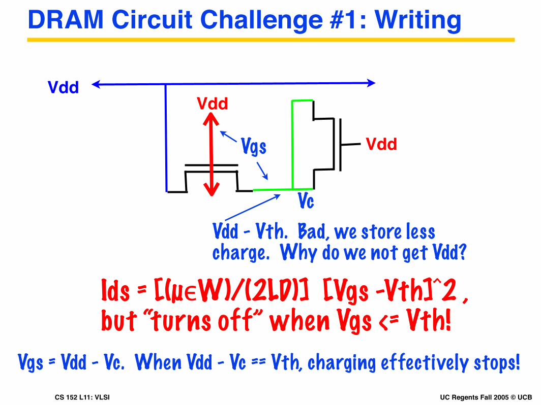
DRAM Circuit Challenge #1: Writing
Vdd
Vdd - Vth. Bad, we store less charge. Why do we not get Vdd?
VddVdd
Ids = [(µεW)/(2LD)] [Vgs -Vth]^2 , but “turns off” when Vgs <= Vth!
Vgs
Vc
Vgs = Vdd - Vc. When Vdd - Vc == Vth, charging effectively stops!
UC Regents Fall 2005 © UCBCS 152 L11: VLSI
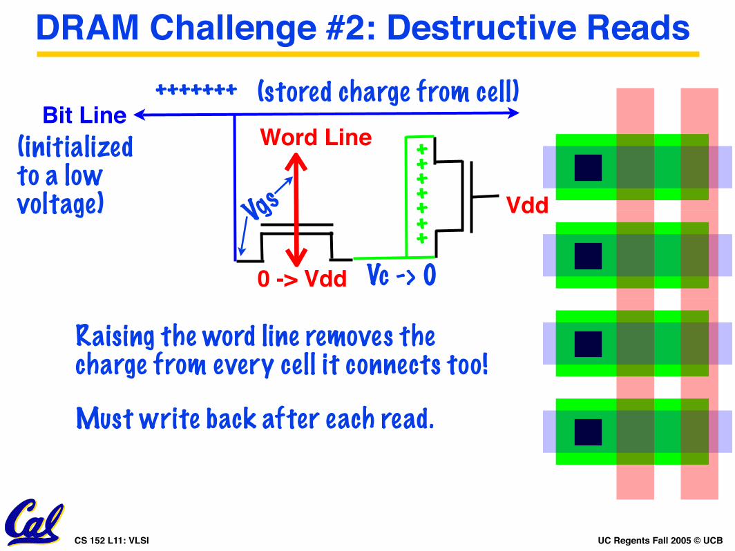
DRAM Challenge #2: Destructive Reads
Vdd
Bit Line
0 -> Vdd Vc -> 0
+++++++
+++++++ (stored charge from cell)
Word Line
Raising the word line removes the charge from every cell it connects too!
Must write back after each read.
Vgs
(initializedto a low voltage)
UC Regents Fall 2005 © UCBCS 152 L11: VLSI
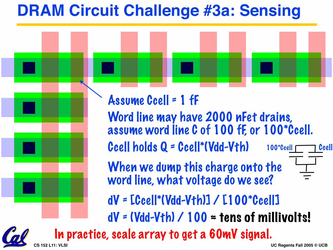
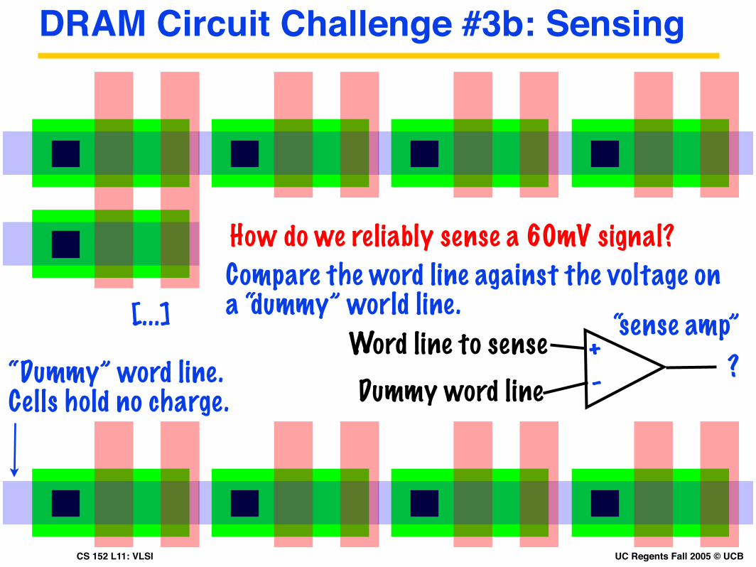
DRAM Circuit Challenge #3a: Sensing
Assume Ccell = 1 fF
Word line may have 2000 nFet drains,assume word line C of 100 fF, or 100*Ccell.
Ccell holds Q = Ccell*(Vdd-Vth)
dV = [Ccell*(Vdd-Vth)] / [100*Ccell]
dV = (Vdd-Vth) / 100 ⋲ tens of millivolts! In practice, scale array to get a 60mV signal.
When we dump this charge onto the word line, what voltage do we see?
Ccell100*Ccell
UC Regents Fall 2005 © UCBCS 152 L11: VLSI
DRAM Circuit Challenge #3b: Sensing
Compare the word line against the voltage on a “dummy” world line.
How do we reliably sense a 60mV signal?
[...]
“Dummy” word line.Cells hold no charge.
?-+Word line to sense
Dummy word line
“sense amp”
UC Regents Fall 2005 © UCBCS 152 L11: VLSI
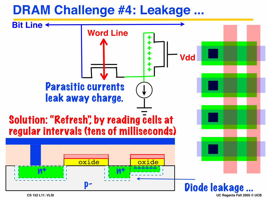
DRAM Challenge #4: Leakage ...
Vdd
Bit Line+++++++
Word Line
p-
oxiden+ n+
oxide------
Parasitic currents leak away charge.
Diode leakage ...
Solution: “Refresh”, by reading cells at regular intervals (tens of milliseconds)
UC Regents Fall 2005 © UCBCS 152 L11: VLSI
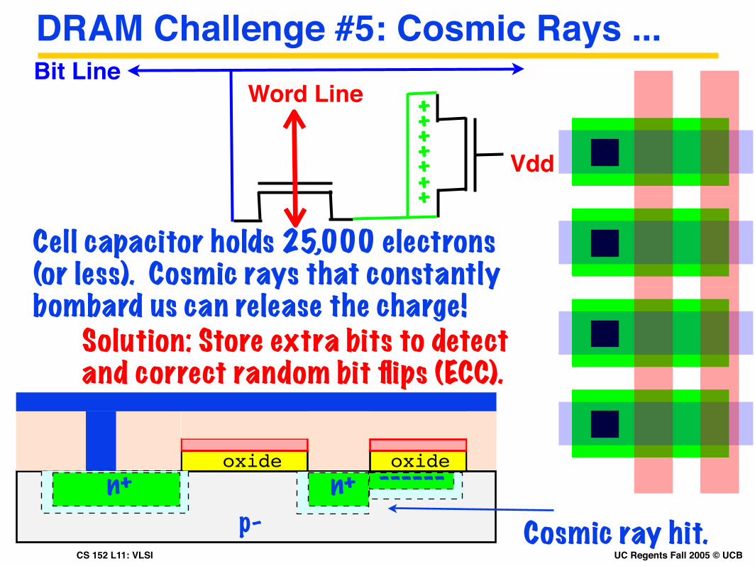
DRAM Challenge #5: Cosmic Rays ...
Vdd
Bit Line+++++++
Word Line
p-
oxiden+ n+
oxide------
Cosmic ray hit.
Solution: Store extra bits to detect and correct random bit flips (ECC).
Cell capacitor holds 25,000 electrons (or less). Cosmic rays that constantly bombard us can release the charge!
UC Regents Fall 2005 © UCBCS 152 L11: VLSI
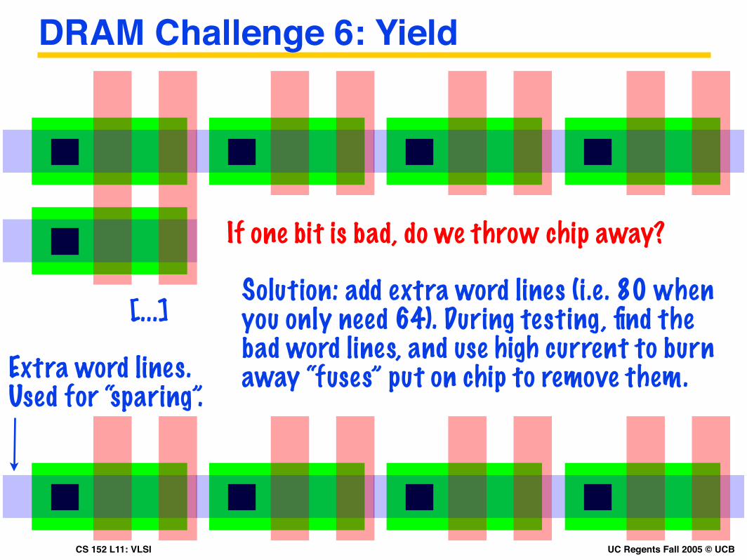
DRAM Challenge 6: Yield
Solution: add extra word lines (i.e. 80 when you only need 64). During testing, find the bad word lines, and use high current to burn away “fuses” put on chip to remove them.
If one bit is bad, do we throw chip away?
[...]
Extra word lines.Used for “sparing”.
UC Regents Fall 2005 © UCBCS 152 L11: VLSI
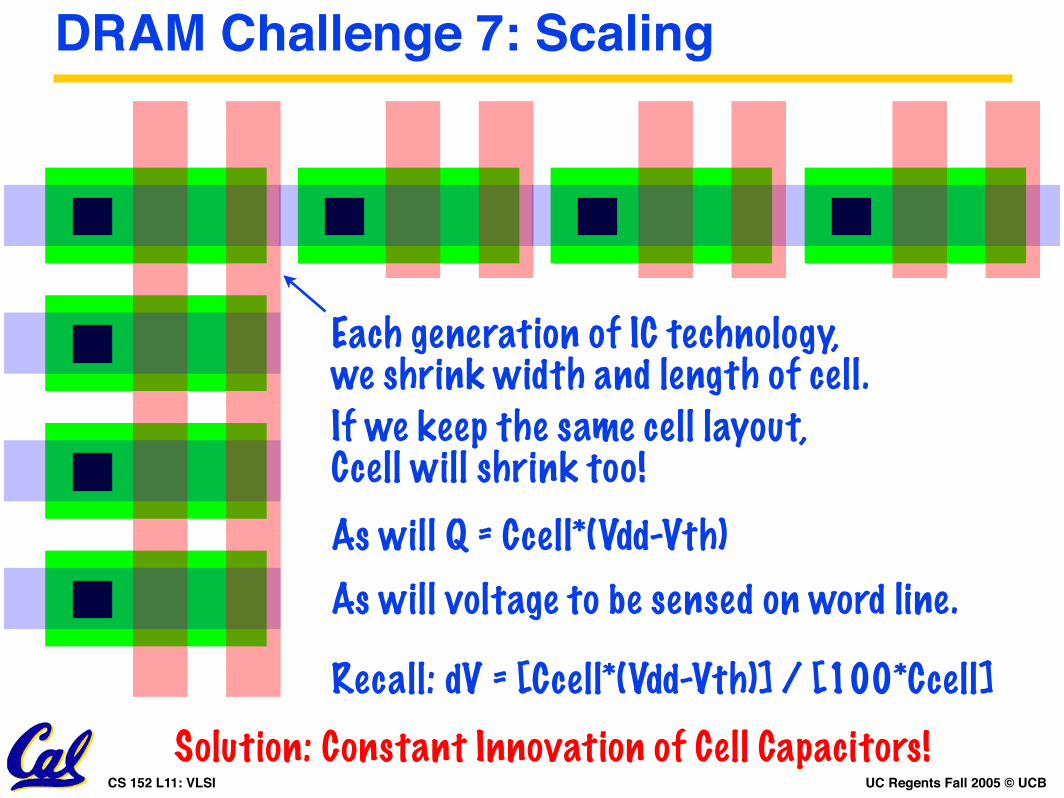
DRAM Challenge 7: Scaling
Each generation of IC technology, we shrink width and length of cell.
As will Q = Ccell*(Vdd-Vth)
As will voltage to be sensed on word line.
Recall: dV = [Ccell*(Vdd-Vth)] / [100*Ccell]
Solution: Constant Innovation of Cell Capacitors!
If we keep the same cell layout, Ccell will shrink too!
UC Regents Fall 2005 © UCBCS 152 L11: VLSI
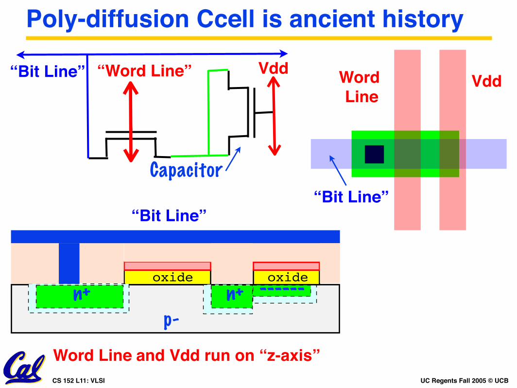
Poly-diffusion Ccell is ancient history
Vdd
Capacitor
“Word Line”“Bit Line”
p-
oxiden+ n+
oxide------
“Bit Line”
Word Line and Vdd run on “z-axis”
Word Line
Vdd
“Bit Line”
UC Regents Fall 2005 © UCBCS 152 L11: VLSI
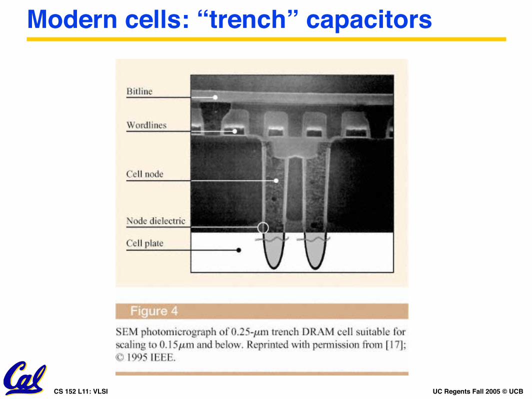
Modern cells: “trench” capacitors
UC Regents Fall 2005 © UCBCS 152 L11: VLSI
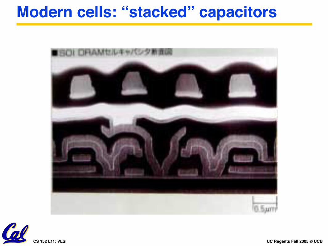
Modern cells: “stacked” capacitors
UC Regents Fall 2005 © UCBCS 152 L11: VLSI
Lessons learned
Capacitors hold state
Drawing transistors
Semiconductor physics
Transistor wrap-up: Fabrication, p-FETs, device model equations.
DRAM: 1 Transistor + 1 Capacitor

UC Regents Fall 2005 © UCBCS 152 L11: VLSI
Lectures: Coming up next ...
Memory array structures and interfaces.
The memory hierarchy