Embed Size (px)
Citation preview
CY8CLED16P01
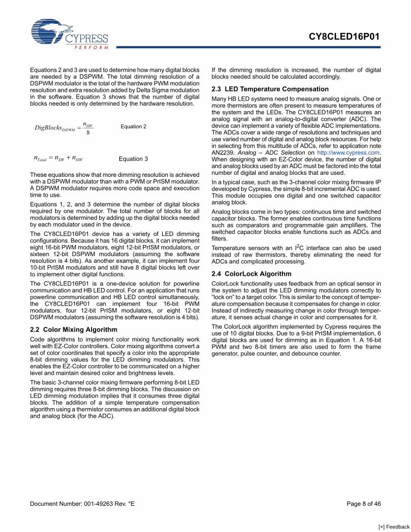
Powerline Communication Solution
Cypress Semiconductor Corporation • 198 Champion Court • San Jose, CA 95134-1709 • 408-943-2600Document Number: 001-49263 Rev. *E Revised October 05, 2009
Features■ Powerline Communication Solution
❐ Integrated Powerline Modem PHY❐ Frequency Shift Keying Modulation❐ Configurable baud rates up to 2400 bps❐ Powerline Optimized Network Protocol❐ Integrates Data Link, Transport, and Network Layers❐ Supports Bidirectional Half Duplex Communication❐ 8-bit CRC Error Detection to Minimize Data Loss❐ I2C enabled Powerline Application Layer❐ Supports I2C Frequencies of 50, 100, and 400 kHz❐ Reference Designs for 110V/240V AC and 12V/24V AC/DC
Powerlines❐ Reference Designs comply with CENELEC EN
50065-1:2001 and FCC Part 15■ HB LED Controller
❐ Configurable Dimmers Support up to 16 Independent LED Channels
❐ 8 to 32 Bits of Resolution per Channel❐ PrISM™ Modulation technology to reduce radiated EMI and
Low Frequency Blinking❐ Additional communication interfaces for lighting control such
as DALI, DMX512 etc.■ Powerful Harvard Architecture Processor
❐ M8C Processor Speeds to 24 MHz❐ Two 8x8 Multiply, 32-Bit Accumulate
■ Programmable System Resources (PSoC® Blocks)
❐ 12 Rail-to-Rail Analog PSoC Blocks provide:• Up to 14-Bit ADCs• Up to 9-Bit DACs• Programmable Gain Amplifiers• Programmable Filters and Comparators
❐ 16 Digital PSoC Blocks provide:• 8 to 32-Bit Timers, Counters, and PWMs• CRC and PRS Modules• Up to Four Full Duplex UARTs• Multiple SPITM Masters or Slaves• Connectable to all GPIO Pins
❐ Complex Peripherals by Combining Blocks■ Flexible On-Chip Memory
❐ 32 KB Flash Program Storage 50,000 Erase or Write Cycles❐ 2 KB SRAM Data Storage❐ EEPROM Emulation in Flash
■ Programmable Pin Configurations❐ 25 mA Sink, 10 mA Source on all GPIO❐ Pull Up, Pull Down, High Z, Strong, or Open Drain Drive
Modes on all GPIO❐ Up to 12 Analog Inputs on GPIO❐ Configurable Interrupt on all GPIO
■ Additional System Resources❐ I2C Slave, Master, and Multi-Master to 400 kHz❐ Watchdog and Sleep Timers❐ User-Configurable Low Voltage Detection
Logic Block DiagramC
Y8C
LED
16P0
1
Powerline Network Protocol
Physical Layer FSK Modem
AC/DC Powerline Coupling Circuit(110V/240V AC, 12V/24V AC/DC etc.)
Powerline
Powerline Communication Solution
Powerline Transceiver Packet
Programmable System Resources
Digital and Analog Peripherals
PSoC Core
Additional System Resources
MAC, Decimator, I2C, SPI, UART etc.
PLC Core
Embedded Application
Modulation Technology
PrISM, PWM etc.
Additional Communication
InterfaceDALI, DMX512
HB LED Controller
[+] Feedback [+] Feedback
CY8CLED16P01
Document Number: 001-49263 Rev. *E Page 2 of 46
1. PLC Functional OverviewThe CY8CLED16P01 is an integrated Powerline Communication(PLC) chip with the Powerline Modem PHY and NetworkProtocol Stack running on the same device. Apart from the PLCcore, the CY8CLED16P01 also offers Cypress's revolutionaryPSoC technology that enables system designers to integratemultiple functions on the same chip.
1.1 Robust Communication using Cypress’s PLC Solution
Powerlines are available everywhere in the world and are awidely available communication medium for PLC technology.The pervasiveness of powerlines also makes it difficult to predictthe characteristics and operation of PLC products. Because ofthe variable quality of powerlines around the world, imple-menting robust communication has been an engineeringchallenge for years. The Cypress PLC solution enables secureand reliable communications. Cypress PLC features that enablerobust communication over powerlines include:
■ Integrated Powerline PHY modem with optimized filters and amplifiers to work with lossy high voltage and low voltage powerlines.
■ Powerline optimized network protocol that supports bidirec-tional communication with acknowledgement-based signaling. In case of data packet loss due to bursty noise on the powerline, the transmitter has the capability to retransmit data.
■ The Powerline Network Protocol also supports an 8-bit CRC for error detection and data packet retransmission.
■ A Carrier Sense Multiple Access (CSMA) scheme is built into the network protocol that minimizes collisions between packet transmissions on the powerline and supports multiple masters and reliable communication on a bigger network.
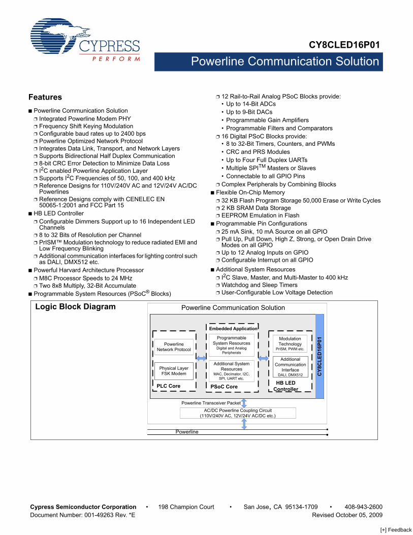
1.2 Powerline Modem PHYFigure 1-1. Physical Layer FSK Modem
The physical layer of the Cypress PLC solution is implementedusing an FSK modem that enables half duplex communicationon any high voltage and low voltage powerline. This modemsupports raw data rates up to 2400 bps. A block diagram isshown in Figure 1-2.
Figure 1-2. Physical Layer FSK Modem Block Diagram
1.2.1 Transmitter SectionDigital data from the network layer is serialized by the digitaltransmitter and fed as input to the modulator. The modulatordivides the local oscillator frequency by a definite factordepending on whether the input data is high level logic ‘1’ or lowlevel logic ‘0’. It then generates a square wave at 133.3 kHz (logic‘0’) or 131.8 kHz (logic ‘1’), which is fed to the ProgrammableGain Amplifier to generate FSK modulated signals. This enablestunable amplification of the signal depending on the noise in thechannel. The logic ‘1’ frequency can also be configured as130.4 kHz for wider FSK deviation.
1.2.2 Receiver SectionThe incoming FSK signal from the powerline is input to a highfrequency (HF) band pass filter that filters out-of-band frequencycomponents and outputs a filtered signal within the desiredspectrum of 125 kHz to 140 kHz for further demodulation. Themixer block multiplies the filtered FSK signals with a locallygenerated signal to produce heterodyned frequencies.The intermediate frequency (IF) band pass filters further removeout-of-band noise as required for further demodulation. Thissignal is fed to the correlator, which produces a DC component(consisting of logic ‘1’ and ‘0’) and a higher frequencycomponent. The output of the correlator is fed to a low pass filter (LPF) thatoutputs only the demodulated digital data at 2400 baud andsuppresses all other higher frequency components generated inthe correlation process. The output of the LPF is digitized by thehysteresis comparator. This eliminates the effects of correlatordelay and false logic triggers due to noise. The digital receiverdeserializes this data and outputs to the network layer for inter-pretation.
CY8
CLE
D16
P01
Powerline Network Protocol
Physical Layer FSK Modem
Powerline Communication Solution
Powerline Transceiver Packet
Programmable System Resources
Digital and Analog Peripherals
PSoC Core
Additional System Resources
MAC, Decimator, I2C, SPI, UART etc.
PLC Core
Embedded Application
Modulation Technology
PrISM, PWM etc.
Additional Communication
InterfaceDALI, DMX512
HB LED Controller
Network Protocol
Coupling Circuit
HF Band Pass Filter
Hysteresis Comparator
Digital Receiver
IF Band Pass Filter
Low Pass Filter
Mixer
Correlator
Pow
erlin
e M
odem
PH
Y
Modulator
Local Oscillator
Logic ‘1’ or Logic ‘0’
Square Wave at FSK
Frequencies
Digital Transmitter
Tran
smitt
er
Rec
eive
r
Local Oscillator
RX Amplifier
Programmable Gain Amplifier
External Low Pass Filter
[+] Feedback [+] Feedback
CY8CLED16P01
Document Number: 001-49263 Rev. *E Page 3 of 46
1.2.3 Coupling Circuit Reference DesignThe coupling circuit couples low voltage signals from theCY8CLED16P01 to the powerline. The topology of this circuit isdetermined by the voltage on the powerline and designconstraints mandated by powerline usage regulations.Cypress provides reference designs for a range of powerlinevoltages including 110V/240V AC and 12V/24V AC/DC. TheCY8CLED16P01 is capable of data communication over otherAC/DC Powerlines as well with the appropriate external couplingcircuit. The 110V AC and 240V AC designs are compliant to thefollowing powerline usage regulations:
■ FCC Part 15 for North America
■ EN 50065-1:2001 for Europe
1.3 Network ProtocolCypress’s powerline optimized network protocol performs thefunctions of the data link, network, and transport layers in anISO/OSI-equivalent model.
Figure 1-3. Powerline Network Protocol
The network protocol implemented on the CY8CLED16P01supports the following features:
■ Bidirectional half duplex communication
■ Master-slave or peer-to-peer network topologies
■ Multiple masters on powerline network
■ 8-bit logical addressing supports up to 256 powerline nodes
■ 16-bit extended logical addressing supports up to 65536 powerline nodes
■ 64-bit physical addressing supports up to 264 powerline nodes
■ Individual, broadcast or group mode addressing
■ Carrier Sense Multiple Access (CSMA)
■ Full control over transmission parameters ❐ Acknowledged❐ Unacknowledged❐ Repeated Transmit
1.3.1 CSMA and Timing Parameters
■ CSMA – The protocol provides the random selection of a period between 85 and 115 ms (out of seven possible values in this range). Within this period, the Band-In-Use (BIU) detector must indicate that the line is not in use, before attempting a trans-mission.
■ BIU – A Band-In-Use detector, as defined under CENELEC EN 50065-1, is active whenever a signal that exceeds 86 dBμVrms anywhere in the range 131.5 kHz to 133.5 kHz is present for at least 4 ms. This threshold can be configured for different end-system applications not requiring CENELEC compliance.The modem tries to retransmit after every 85 to 115 ms when the band is in use. The transmitter times out after 1.1 seconds to 3 seconds (depending on the noise on the Powerline) and generates an interrupt to indicate that the trans-mitter was unable to acquire the powerline.
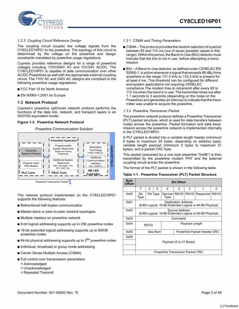
1.3.2 Powerline Transceiver PacketThe powerline network protocol defines a Powerline Transceiver(PLT) packet structure, which is used for data transfers betweennodes across the powerline. Packet formation and data trans-mission across the powerline network is implemented internallyin the CY8CLED16P01. A PLT packet is divided into a variable length header (minimum6 bytes to maximum 20 bytes, depending on address type),variable length payload (minimum 0 bytes to maximum 31bytes), and a packet CRC byte.This packet (preceded by a one byte preamble "0xAB") is thentransmitted by the powerline modem PHY and the externalcoupling circuit across the powerline.The format of the PLT packet is shown in the following table.C
Y8C
LED
16P0
1
Powerline Network Protocol
Physical Layer FSK Modem
Powerline Communication Solution
Powerline Transceiver Packet
Programmable System Resources
Digital and Analog Peripherals
PSoC Core
Additional System Resources
MAC, Decimator, I2C, SPI, UART etc.
PLC Core
Embedded Application
Modulation Technology
PrISM, PWM etc.
Additional Communication
InterfaceDALI, DMX512
HB LED Controller Table 1-1. Powerline Transceiver (PLT) Packet Structure
Byte Offset Bit Offset
7 6 5 4 3 2 1 00x00 SA
TypeDA Type Service
TypeRSVD RSVD Response RSVD
0x01 Destination Address (8-Bit Logical, 16-Bit Extended Logical or 64-Bit Physical)
0x02 Source Address (8-Bit Logical, 16-Bit Extended Logical or 64-Bit Physical)
0x03 Command0x04 RSVD Payload Length
0x05 Seq Num Powerline Packet Header CRC0x06
Payload (0 to 31 Bytes)
Powerline Transceiver Packet CRC
[+] Feedback [+] Feedback
CY8CLED16P01
Document Number: 001-49263 Rev. *E Page 4 of 46
1.3.3 Packet HeaderThe packet header contains the first 6 bytes of the packet when1-byte logical addressing is used. When 8-byte physicaladdressing is used, the source and destination addresses eachcontain 8 bytes. In this case, the header can consist of amaximum of 20 bytes. Unused fields marked RSVD are for futureexpansion and are transmitted as bit 0. Table 1-2 describes thePLT packet header fields in detail.Table 1-2. Powerline Transceiver (PLT) Packet Header
1.3.4 PayloadThe packet payload has a length of 0 to 31 bytes. Payloadcontent is user defined and can be read or written through I2C.
1.3.5 Packet CRCThe last byte of the packet is an 8-bit CRC value used to checkpacket data integrity. This CRC calculation includes the headerand payload portions of the packet and is in addition to thepowerline packet header CRC.
1.3.6 Sequence NumberingThe sequence number is increased for every new unique packettransmitted. If in acknowledged mode and an acknowledgmentis not received for a given packet, that packet will be re-trans-mitted (if TX_Retry > 0) with the same sequence number. If inunacknowledged mode, the packet will be transmitted (TX_Retry+ 1) times with the same sequence number.If the receiver receives consecutive packets from the samesource address with the same sequence number and packetCRC, it does not notify the host of the reception of the duplicatepacket. If in acknowledged mode, it still sends an acknowl-edgment so that the transmitter knows that the packet wasreceived.
1.3.7 AddressingThe CY8CLED16P01 has three modes of addressing:
■ Logical addressing: Every CY8CLED16P01 node can have either a 8-bit logical address or a 16-bit logical address. The logical address of the PLC Node is set by the local application or by a remote node on the Powerline.
■ Physical addressing: Every CY8CLED16P01 has a unique 64-bit physical address.
■ Group addressing: This is explained in the next section.
1.3.8 Group MembershipGroup membership enables the user to multicast messages toselect groups. The CY8CLED16P01 supports two types of groupaddressing:
■ Single Group Membership – The network protocol supports up to 256 different groups on the network in this mode. In this mode, each PLC node can only be part of a single group. For example, multiple PLC nodes can be part of Group 131.
■ Multiple Group Membership – The network protocol supports eight different groups in this mode and each PLC node can be a part of multiple groups. For example, a single PLC node can be a part of Group 3, Group 4, and Group 7 at the same time.
Both of these membership modes can also be used together forgroup membership. For example, a single PLC node can be apart of Group 131 and also multiple groups such as Group 3,Group 4, and Group 7. The group membership ID for broadcasting messages to allnodes in the network is 0x00. The service type is always set to Unacknowledgment Mode inGroup Addressing Mode. This is to avoid acknowledgmentflooding on the powerline during multicast.
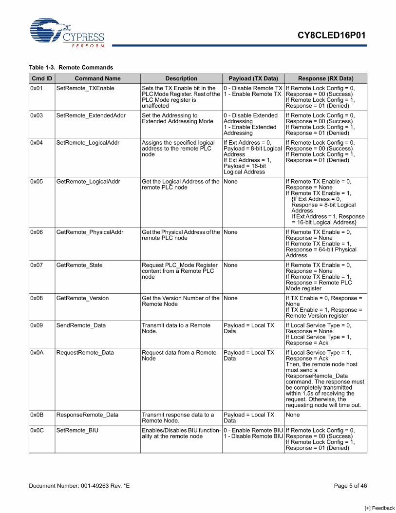
1.3.9 Remote CommandsIn addition to sending normal data over the Powerline, theCY8CPLC10 can also send (and request) control information to(and from) another node on the network. The type of remotecommand to transmit is set by the TX_CommandID register andwhen received, is stored in the RX_CommandID register.When a control command (Command ID = 0x01 - 0x08 and 0x0C- 0x0F) is received, the protocol will automatically process thepacket (if Lock_Configuration is '0'), respond to the initiator, andnotify the host of the successful transmission and reception.When the send data command (ID 0x09) or request for datacommand (ID 0x0A) is received, the protocol will reply with anacknowledgment packet (if TX_Service_Type = '1'), and notifythe host of the new received data. If the initiator doesn't receivethe acknowledgment packet within 500ms, it will notify the hostof the no acknowledgment received condition.When a response command (ID 0x0B) is received by the initiatorwithin 1.5s of sending the request for data command, theprotocol will notify the host of the successful transmission andreception. If the response command is not received by theinitiator within 1.5s, it will notify the host of the no responsereceived condition.The host is notified by updating the appropriate values in theINT_Status register (including Status_Value_Change).The command IDs 0x30-0xff can be used for custom commandsthat would be processed by the external host (e.g. set an LEDcolor, get a temperature/voltage reading). The available remotecommands are described in Table 1-3 on page 5 with therespective Command IDs.
Field Name
No. of Bits Tag Description
SA Type 1 Source Address Type
0 – Logical Addressing1 – Physical Addressing
DA Type 2 Destination Address Type
00 – Logical Addressing01 – Group Addressing10 – Physical Addressing11 – Invalid
Service Type
1 0 – Unacknowledged Messaging1 – Acknowledged Messaging
Response 1 Response 0 - Not an acknowledgement or response packet1 - Acknowledgement or response packet
Seq Num 4 Sequence Number
4-bit unique identifier for each packet between source and desti-nation.
Header CRC
4 4-bit CRC value. This enables the receiver to suspend receiving the rest of the packet if its header is corrupted
[+] Feedback [+] Feedback
CY8CLED16P01
Document Number: 001-49263 Rev. *E Page 5 of 46
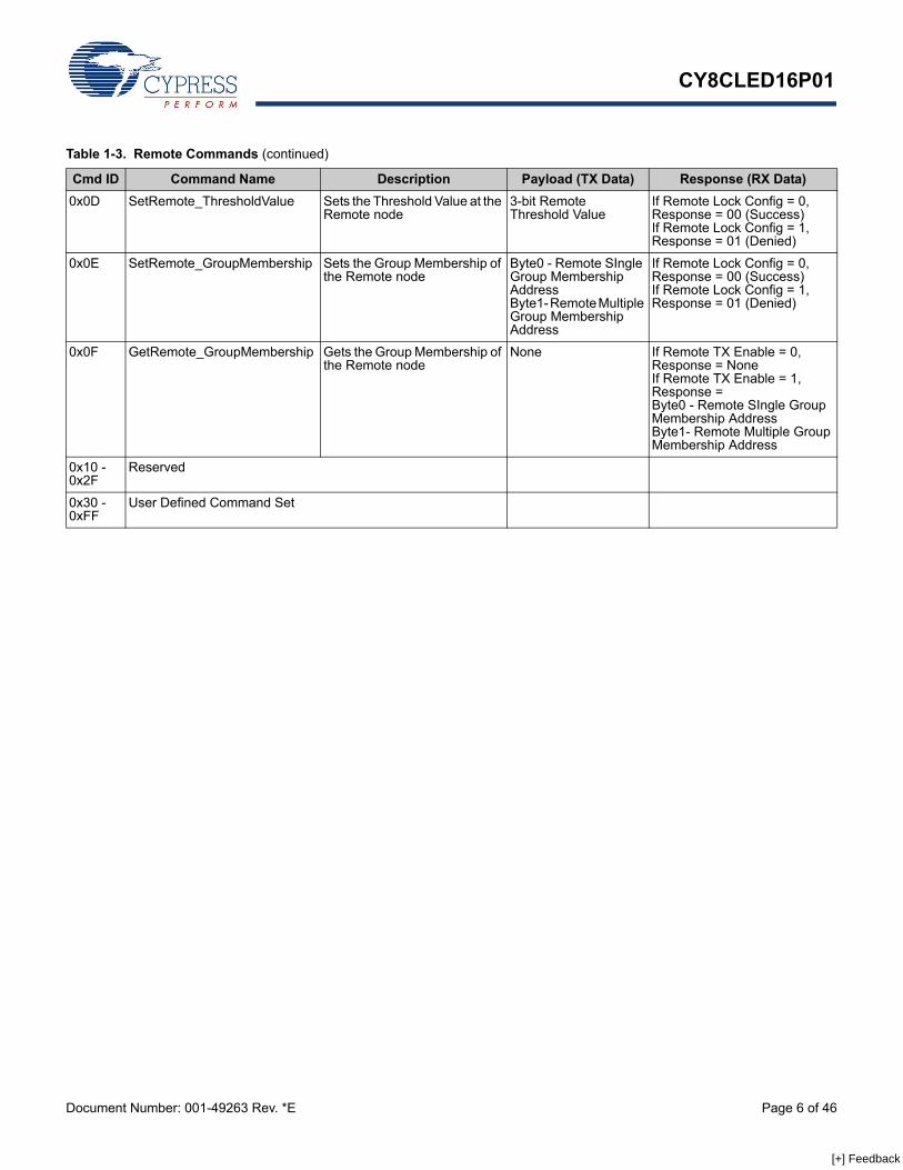
Table 1-3. Remote Commands
Cmd ID Command Name Description Payload (TX Data) Response (RX Data)0x01 SetRemote_TXEnable Sets the TX Enable bit in the
PLC Mode Register. Rest of the PLC Mode register is unaffected
0 - Disable Remote TX1 - Enable Remote TX
If Remote Lock Config = 0, Response = 00 (Success)If Remote Lock Config = 1, Response = 01 (Denied)
0x03 SetRemote_ExtendedAddr Set the Addressing to Extended Addressing Mode
0 - Disable Extended Addressing1 - Enable Extended Addressing
If Remote Lock Config = 0, Response = 00 (Success)If Remote Lock Config = 1, Response = 01 (Denied)
0x04 SetRemote_LogicalAddr Assigns the specified logical address to the remote PLC node
If Ext Address = 0, Payload = 8-bit Logical AddressIf Ext Address = 1, Payload = 16-bit Logical Address
If Remote Lock Config = 0, Response = 00 (Success)If Remote Lock Config = 1, Response = 01 (Denied)
0x05 GetRemote_LogicalAddr Get the Logical Address of the remote PLC node
None If Remote TX Enable = 0, Response = NoneIf Remote TX Enable = 1,
{If Ext Address = 0, Response = 8-bit Logical AddressIf Ext Address = 1, Response = 16-bit Logical Address}
0x06 GetRemote_PhysicalAddr Get the Physical Address of the remote PLC node
None If Remote TX Enable = 0, Response = NoneIf Remote TX Enable = 1, Response = 64-bit Physical Address
0x07 GetRemote_State Request PLC_Mode Register content from a Remote PLC node
None If Remote TX Enable = 0, Response = NoneIf Remote TX Enable = 1, Response = Remote PLC Mode register
0x08 GetRemote_Version Get the Version Number of the Remote Node
None If TX Enable = 0, Response = NoneIf TX Enable = 1, Response = Remote Version register
0x09 SendRemote_Data Transmit data to a Remote Node.
Payload = Local TX Data
If Local Service Type = 0, Response = NoneIf Local Service Type = 1, Response = Ack
0x0A RequestRemote_Data Request data from a Remote Node
Payload = Local TX Data
If Local Service Type = 1, Response = AckThen, the remote node host must send a ResponseRemote_Data command. The response must be completely transmitted within 1.5s of receiving the request. Otherwise, the requesting node will time out.
0x0B ResponseRemote_Data Transmit response data to a Remote Node.
Payload = Local TX Data
None
0x0C SetRemote_BIU Enables/Disables BIU function-ality at the remote node
0 - Enable Remote BIU1 - Disable Remote BIU
If Remote Lock Config = 0, Response = 00 (Success)If Remote Lock Config = 1, Response = 01 (Denied)
[+] Feedback [+] Feedback
CY8CLED16P01
Document Number: 001-49263 Rev. *E Page 6 of 46
0x0D SetRemote_ThresholdValue Sets the Threshold Value at the Remote node
3-bit Remote Threshold Value
If Remote Lock Config = 0, Response = 00 (Success)If Remote Lock Config = 1, Response = 01 (Denied)
0x0E SetRemote_GroupMembership Sets the Group Membership of the Remote node
Byte0 - Remote SIngle Group Membership AddressByte1- Remote Multiple Group Membership Address
If Remote Lock Config = 0, Response = 00 (Success)If Remote Lock Config = 1, Response = 01 (Denied)
0x0F GetRemote_GroupMembership Gets the Group Membership of the Remote node
None If Remote TX Enable = 0, Response = NoneIf Remote TX Enable = 1, Response = Byte0 - Remote SIngle Group Membership AddressByte1- Remote Multiple Group Membership Address
0x10 - 0x2F
Reserved
0x30 - 0xFF
User Defined Command Set
Table 1-3. Remote Commands (continued)
Cmd ID Command Name Description Payload (TX Data) Response (RX Data)
[+] Feedback [+] Feedback
CY8CLED16P01
Document Number: 001-49263 Rev. *E Page 7 of 46
2. High Brightness (HB) LED ControllerFigure 2-1. CY8CLED16P01: HB LED Controller
The HB LED Controller is based on Cypress's EZ-Color™technology. EZ-Color offers the ideal control solution for highbrightness (HB) LED applications requiring intelligent dimmingcontrol. EZ-Color devices combine the power and flexibility ofPSoC (Programmable System-on-Chip) with Cypress's PrISM™(Precise Illumination Signal Modulation) modulation technologyproviding lighting designers a fully customizable and integratedlighting solution platform.The CY8CLED16P01 supports up to 16 independent LEDchannels with up to 32 bits of resolution per channel, givinglighting designers the flexibility to choose the LED array size andcolor quality. PSoC Designer software, with lighting-specific usermodules, significantly cuts development time and simplifiesimplementation of fixed color points through temperature andLED binning compensation. EZ-Color's virtually limitless analogand digital customization enable simple integration of features inaddition to intelligent lighting, such as battery charging, imagestabilization, and motor control during the development process.These features, along with Cypress's best-in-class quality anddesign support, make EZ-Color the ideal choice for intelligent HBLED control applications.The list of functions that EZ-Color devices implement are:
■ LED Dimming Modulation
■ Pulse Density Modulation Techniques❐ DMX512❐ DALI
■ Digital Communication for Lighting
■ LED Temperature Compensation
■ 3- and 4-Channel Color Mixing❐ Including LED Binning Compensation
■ Optical Feedback Algorithms
2.1 LED Dimming ModulationThe LED Dimming modulators are an important part of any HBLED application. All EZ-Color controllers are capable of threeprimary types of LED dimming modulations. These are:■ Pulse Width Modulation (PWM)■ Precise Illumination Signal Modulation (PrISM)■ Delta Sigma Modulated PWM (DSPWM)PWM is among the most commonly used and conventionalmethods of modulation. It is straightforward to use and effectivein practice. There are two additional techniques of modulationsupported by EZ-Color that are superior to using the PWM alone: ■ PrISM is a modulation technique that is developed and
patented by Cypress. It results in reduced EMI as compared to the PWM technique while still providing adequate dimming control for LEDs.
■ The Delta Sigma Modulated PWM technique provides higher resolution while using the same hardware resources as a conventional PWM.
LED dimming modulators use digital block resources. Digitalblocks are configurable 8-bit digital peripherals. There are twotypes of digital blocks in the CY8CLED16P01: basic and commu-nication. Usually, there are equal numbers of each. Any commu-nication functions must be implemented using communicationblocks but basic, noncommunication functions are implementedusing either kind of block.PWM and DSPWM modulators can have a dimming resolutionof up to 16 bits. A PrISM modulator can theoretically have adimming resolution of up to 32 bits, but the maximum recom-mended resolution for these modulators is 13 bits. This isbecause the output signal of a PrISM modulator has a frequencyoutput range that increases with the resolution of the modulator.This increase in frequency output range is undesirable as it goesbeyond the switching frequency of the current driver. Therefore,a resolution of 13 bits or lower is recommended for a PrISMmodulator. Refer to application note AN47372, PrISMTechnology for LED Dimming on http://www.cypress.com, fordetails. To determine the number of digital blocks used by one PWM orPrISM modulator, use Equation 1. Note that a partial digital blockcannot be used, so the result must always be rounded up. InEquation 1, n is the dimming resolution of the modulator. Theresolution of dimming is determined by the color accuracyneeded for the end application.
CY8
CLE
D16
P01
Powerline Network Protocol
Physical Layer FSK Modem
Powerline Communication Solution
Powerline Transceiver Packet
Programmable System Resources
Digital and Analog Peripherals
PSoC Core
Additional System Resources
MAC, Decimator, I2C, SPI, UART etc.
PLC Core
Embedded Application
Modulation Technology
PrISM, PWM etc.
Additional Communication
InterfaceDALI, DMX512
HB LED Controller
8,nDigBlocks PRISMPWM = Equation 1
[+] Feedback [+] Feedback
CY8CLED16P01
Document Number: 001-49263 Rev. *E Page 8 of 46
Equations 2 and 3 are used to determine how many digital blocksare needed by a DSPWM. The total dimming resolution of aDSPWM modulator is the total of the hardware PWM modulationresolution and extra resolution added by Delta Sigma modulationin the software. Equation 3 shows that the number of digitalblocks needed is only determined by the hardware resolution.
These equations show that more dimming resolution is achievedwith a DSPWM modulator than with a PWM or PrISM modulator.A DSPWM modulator requires more code space and executiontime to use.Equations 1, 2, and 3 determine the number of digital blocksrequired by one modulator. The total number of blocks for allmodulators is determined by adding up the digital blocks neededby each modulator used in the device. The CY8CLED16P01 device has a variety of LED dimmingconfigurations. Because it has 16 digital blocks, it can implementeight 16-bit PWM modulators, eight 12-bit PrISM modulators, orsixteen 12-bit DSPWM modulators (assuming the softwareresolution is 4 bits). As another example, it can implement four10-bit PrISM modulators and still have 8 digital blocks left overto implement other digital functions.The CY8CLED16P01 is a one-device solution for powerlinecommunication and HB LED control. For an application that runspowerline communication and HB LED control simultaneously,the CY8CLED16P01 can implement four 16-bit PWMmodulators, four 12-bit PrISM modulators, or eight 12-bitDSPWM modulators (assuming the software resolution is 4 bits).
2.2 Color Mixing AlgorithmCode algorithms to implement color mixing functionality workwell with EZ-Color controllers. Color mixing algorithms convert aset of color coordinates that specify a color into the appropriate8-bit dimming values for the LED dimming modulators. Thisenables the EZ-Color controller to be communicated on a higherlevel and maintain desired color and brightness levels. The basic 3-channel color mixing firmware performing 8-bit LEDdimming requires three 8-bit dimming blocks. The discussion onLED dimming modulation implies that it consumes three digitalblocks. The addition of a simple temperature compensationalgorithm using a thermistor consumes an additional digital blockand analog block (for the ADC).
If the dimming resolution is increased, the number of digitalblocks needed should be calculated accordingly.
2.3 LED Temperature CompensationMany HB LED systems need to measure analog signals. One ormore thermistors are often present to measure temperatures ofthe system and the LEDs. The CY8CLED16P01 measures ananalog signal with an analog-to-digital converter (ADC). Thedevice can implement a variety of flexible ADC implementations.The ADCs cover a wide range of resolutions and techniques anduse varied number of digital and analog block resources. For helpin selecting from this multitude of ADCs, refer to application noteAN2239, Analog – ADC Selection on http://www.cypress.com.When designing with an EZ-Color device, the number of digitaland analog blocks used by an ADC must be factored into the totalnumber of digital and analog blocks that are used.In a typical case, such as the 3-channel color mixing firmware IPdeveloped by Cypress, the simple 8-bit incremental ADC is used.This module occupies one digital and one switched capacitoranalog block. Analog blocks come in two types: continuous time and switchedcapacitor blocks. The former enables continuous time functionssuch as comparators and programmable gain amplifiers. Theswitched capacitor blocks enable functions such as ADCs andfilters. Temperature sensors with an I2C interface can also be usedinstead of raw thermistors, thereby eliminating the need forADCs and complicated processing.
2.4 ColorLock AlgorithmColorLock functionality uses feedback from an optical sensor inthe system to adjust the LED dimming modulators correctly to“lock on” to a target color. This is similar to the concept of temper-ature compensation because it compensates for change in color.Instead of indirectly measuring change in color through temper-ature, it senses actual change in color and compensates for it. The ColorLock algorithm implemented by Cypress requires theuse of 10 digital blocks. Due to a 9-bit PrISM implementation, 6digital blocks are used for dimming as in Equation 1. A 16-bitPWM and two 8-bit timers are also used to form the framegenerator, pulse counter, and debounce counter.
Equation 28HW
DSPWMnDigBlocks =
Equation 3HWSWTotal nnn +=
[+] Feedback [+] Feedback
CY8CLED16P01
Document Number: 001-49263 Rev. *E Page 9 of 46
2.5 Digital CommunicationMost HB LED-based lighting systems require some form ofdigital communication to send and receive data to and from thelight fixtures to control them. The CY8CLED16P01 is aone-device solution for HB LED lighting control and powerlinecommunication. However, the CY8CLED16P01 supportsseveral other data communication protocols, apart frompowerline communication. These are listed in Table 2-1. Someof the hardware is dedicated for a protocol and does not use anydigital blocks. Some protocols use digital blocks to implement thecommunication. A DMX512 protocol receiver can be implemented using twodigital blocks. This is a standard protocol that is common in stageand concert lighting systems. The receiver has a softwareprogrammable address and programmable number of channelsthat it can control. A typical DMX512 receiver implementation(developed by Cypress) controlling three LED channelsconsumes five digital blocks (three for the LED modulators).Table 2-1. Digital Communication Resource Usage
DALI is another lighting communication protocol that is commonfor large commercial buildings. The DALI slave can be imple-mented in EZ-Color consuming six digital blocks (three for theDALI slave and three to modulate 3 LED channels). The threeblocks used to implement DALI need not be communicationblocks as the Manchester encoding is performed in the software.
Apart from these specific lighting communication protocols, theindustry standard communication protocols such as I2C, UART,and SPI can be implemented in any of the devices in the family.As examples, SPI can be used to interface to external WUSBdevices, while I2C can be used to interface to external microcon-trollers. Table 2-1 also shows the number of digital block resources thateach type of communication block consumes.
2.6 Other FunctionsThe CY8CLED16P01 is capable of functions other than thosepreviously discussed. Most functions that can be implementedwith a standard microcontroller can be also implemented with theCY8CLED16P01. Similar to regular PSoC devices, the CY8CLED16P01 also hasdynamic reconfiguration ability. This is a technique that enablesthe device’s digital and analog resources to be reused fordifferent functions that may not be available simultaneously. Forinstance, consider the application to remotely control LEDcolor/intensity (with current feedback) over powerlines using theCY8CLED16P01 for both PLC and LED color control. The PLCfunctionality and the current feedback do not necessarily need tohappen at the same time. Therefore, the digital and analogblocks that implement the PLC functionality can dynamicallyreconfigure into resources that implement current feedback. Bydoing this, the CY8CLED16P01 device gets more functionalityout of a fixed number of resources than would otherwise bepossible. The only constraint on this technique is the amount ofFlash and SRAM size required for the code to implement thesefunctions. For more details on dynamic reconfiguration, refer toapplication note AN2104, PSoC Dynamic Reconfiguration.
Data Protocol Digital Blocks CommunicationDigital Blocks
DMX512 (Receiver) 2 1
DALI (Slave) 3 0
I2C Master or Slave 0 0
Half Duplex UART 1 1
SPI Master or Slave 1 1
[+] Feedback [+] Feedback
CY8CLED16P01
Document Number: 001-49263 Rev. *E Page 10 of 46
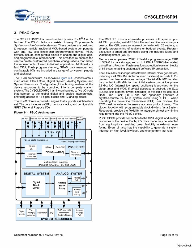
3. PSoC CoreThe CY8CLED16P01 is based on the Cypress PSoC® 1 archi-tecture. The PSoC platform consists of many ProgrammableSystem-on-chip Controller devices. These devices are designedto replace multiple traditional MCU-based system componentswith one, low cost single-chip programmable device. PSoCdevices include configurable blocks of analog and digital logic,and programmable interconnects. This architecture enables theuser to create customized peripheral configurations that matchthe requirements of each individual application. Additionally, afast CPU, Flash program memory, SRAM data memory, andconfigurable I/Os are included in a range of convenient pinoutsand packages.The PSoC architecture, as shown in Figure 3-1., consists of fourmain areas: PSoC Core, Digital System, Analog System, andSystem Resources. Configurable global busing enables all thedevice resources to be combined into a complete customsystem. The CY8CLED16P01 family can have up to five I/O portsthat connect to the global digital and analog interconnects,providing access to 16 digital blocks and 12 analog blocks.The PSoC Core is a powerful engine that supports a rich featureset. The core includes a CPU, memory, clocks, and configurableGPIO (General Purpose I/O).
Figure 3-1. PSoC Architecture
The M8C CPU core is a powerful processor with speeds up to24 MHz, providing a 4 MIPS 8-bit Harvard architecture micropro-cessor. The CPU uses an interrupt controller with 25 vectors, tosimplify programming of realtime embedded events. Programexecution is timed and protected using the included Sleep andWatchdog timers (WDT).Memory encompasses 32 KB of Flash for program storage, 2 KBof SRAM for data storage, and up to 2 KB of EEPROM emulatedusing Flash. Program Flash uses four protection levels on blocksof 64 bytes, enabling customized software IP protection.The PSoC device incorporates flexible internal clock generators,including a 24 MHz IMO (internal main oscillator) accurate to 2.5percent over temperature and voltage. The 24 MHz IMO can alsobe doubled to 48 MHz for the digital system use. A low power32 kHz ILO (internal low speed oscillator) is provided for thesleep timer and WDT. If crystal accuracy is desired, the ECO(32.768 kHz external crystal oscillator) is available for use as aReal Time Clock (RTC) and can optionally generate acrystal-accurate 24 MHz system clock using a PLL. Whenoperating the Powerline Transceiver (PLT) user module, theECO must be selected to ensure accurate protocol timing. Theclocks, together with programmable clock dividers (as a SystemResource), provide the flexibility to integrate almost any timingrequirement into the PSoC device.PSoC GPIOs provide connection to the CPU, digital, and analogresources of the device. Each pin’s drive mode may be selectedfrom eight options, enabling great flexibility in external inter-facing. Every pin also has the capability to generate a systeminterrupt on high level, low level, and change from last read.
DIGITAL SYSTEM
SRAM2K
InterruptController
Sleep andWatchdog
Multiple Clock Sources(Includes IMO, ILO, PLL, and ECO)
Global Digital InterconnectGlobal Analog Interconnect
PSoC CORE
CPU Core (M8C)
SROM Flash 32K
DigitalBlockArray
TwoMultiply
Accums.
InternalVoltage
Ref.
DigitalClocks
POR and LVD
System ResetsDecimator
SYSTEM RESOURCES
ANALOG SYSTEM
AnalogBlockArray
AnalogRef.
AnalogInput
Muxing
I C2
Port 7 Port 6 Port 5 Port 4 Port 3 Port 2 Port 1 Port 0 AnalogDrivers
SYSTEM BUS
[+] Feedback [+] Feedback
CY8CLED16P01
Document Number: 001-49263 Rev. *E Page 11 of 46
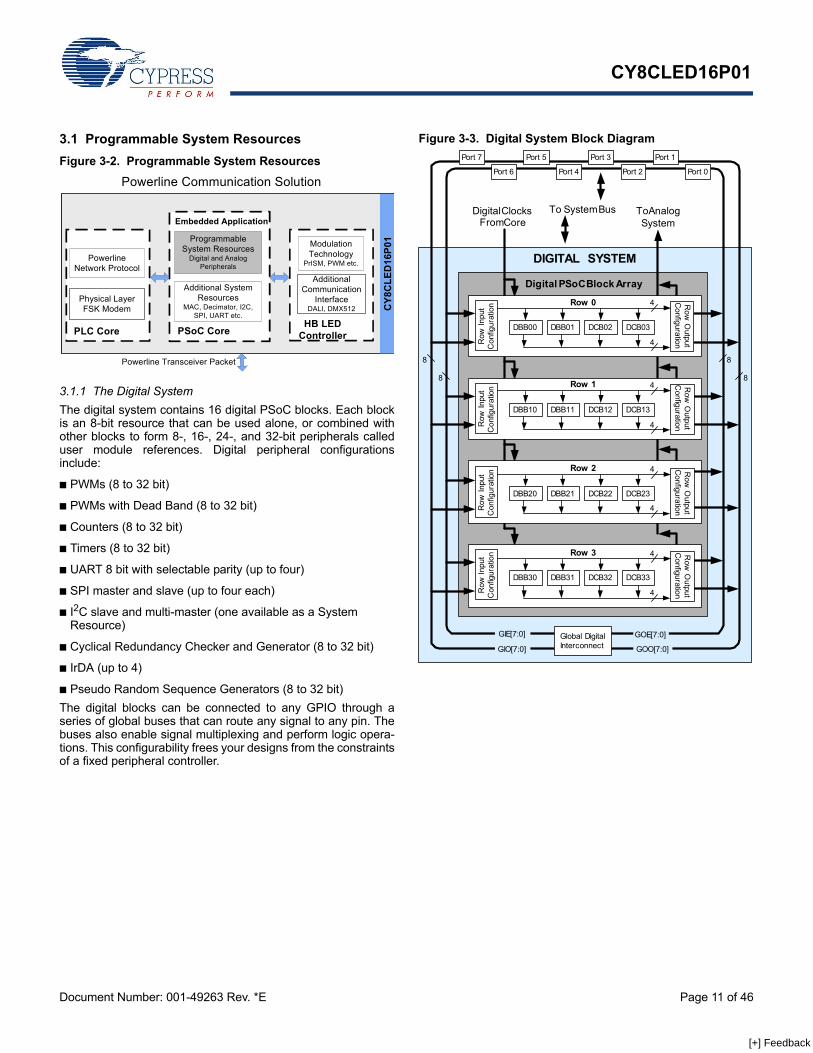
3.1 Programmable System ResourcesFigure 3-2. Programmable System Resources
3.1.1 The Digital SystemThe digital system contains 16 digital PSoC blocks. Each blockis an 8-bit resource that can be used alone, or combined withother blocks to form 8-, 16-, 24-, and 32-bit peripherals calleduser module references. Digital peripheral configurationsinclude:
■ PWMs (8 to 32 bit)
■ PWMs with Dead Band (8 to 32 bit)
■ Counters (8 to 32 bit)
■ Timers (8 to 32 bit)
■ UART 8 bit with selectable parity (up to four)
■ SPI master and slave (up to four each)
■ I2C slave and multi-master (one available as a System Resource)
■ Cyclical Redundancy Checker and Generator (8 to 32 bit)
■ IrDA (up to 4)
■ Pseudo Random Sequence Generators (8 to 32 bit)The digital blocks can be connected to any GPIO through aseries of global buses that can route any signal to any pin. Thebuses also enable signal multiplexing and perform logic opera-tions. This configurability frees your designs from the constraintsof a fixed peripheral controller.
Figure 3-3. Digital System Block Diagram
CY8
CLE
D16
P01
Powerline Network Protocol
Physical Layer FSK Modem
Powerline Communication Solution
Powerline Transceiver Packet
Programmable System Resources
Digital and Analog Peripherals
PSoC Core
Additional System Resources
MAC, Decimator, I2C, SPI, UART etc.
PLC Core
Embedded Application
Modulation Technology
PrISM, PWM etc.
Additional Communication
InterfaceDALI, DMX512
HB LED Controller
DIGITAL SYSTEM
To System BusDigital ClocksFrom Core
Digital PSoC Block Array
To AnalogSystem
8
Row
Inpu
tC
onfig
urat
ion R
ow O
utputC
onfiguration
88
8
Row 1
DBB10 DBB11 DCB12 DCB13
Row
Inpu
tC
onfig
urat
ion 4
4
Row
Output
Configuration
Row
Inpu
tC
onfig
urat
ion R
ow O
utputC
onfiguration
Row 2
DBB20 DBB21 DCB22 DCB23
4
4
Row 0
DBB00 DBB01 DCB02 DCB03
4
4
Row
Inpu
tC
onfig
urat
ion R
ow O
utputC
onfiguration
Row 3
DBB30 DBB31 DCB32 DCB33
4
4
GIE[7:0]
GIO[7:0]
GOE[7:0]
GOO[7:0]Global DigitalInterconnect
Port 7
Port 6
Port 5
Port 4
Port 3
Port 2
Port 1
Port 0
[+] Feedback [+] Feedback
CY8CLED16P01
Document Number: 001-49263 Rev. *E Page 12 of 46
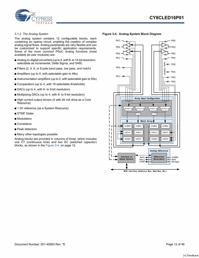
3.1.2 The Analog SystemThe analog system contains 12 configurable blocks, eachcontaining an opamp circuit, enabling the creation of complexanalog signal flows. Analog peripherals are very flexible and canbe customized to support specific application requirements.Some of the more common PSoC analog functions (mostavailable as user modules) are:
■ Analog-to-digital converters (up to 4, with 6- to 14-bit resolution, selectable as Incremental, Delta Sigma, and SAR)
■ Filters (2, 4, 6, or 8 pole band pass, low pass, and notch)
■ Amplifiers (up to 4, with selectable gain to 48x)
■ Instrumentation amplifiers (up to 2, with selectable gain to 93x)
■ Comparators (up to 4, with 16 selectable thresholds)
■ DACs (up to 4, with 6- to 9-bit resolution)
■ Multiplying DACs (up to 4, with 6- to 9-bit resolution)
■ High current output drivers (4 with 40 mA drive as a Core Resource)
■ 1.3V reference (as a System Resource)
■ DTMF Dialer
■ Modulators
■ Correlators
■ Peak detectors
■ Many other topologies possibleAnalog blocks are provided in columns of three, which includesone CT (continuous time) and two SC (switched capacitor)blocks, as shown in the Figure 3-4. on page 12.
Figure 3-4. Analog System Block Diagram
ACB00 ACB01
Block Array
Array Input Configuration
ACI1[1:0] ACI2[1:0]
ACB02 ACB03
ASC12 ASD13
ASD22 ASC23ASD20
ACI0[1:0] ACI3[1:0]
P0[6]
P0[4]
P0[2]
P0[0]
P2[2]
P2[0]
P2[6]
P2[4]
Ref
InAG
ND
In
P0[7]
P0[5]
P0[3]
P0[1]
P2[3]
P2[1]
ReferenceGenerators
AGNDInRefInBandgap
RefHiRefLoAGND
ASD11
ASC21
ASC10
Interface toDigital System
M8C Interface (Address Bus, Data Bus, Etc.)
Analog Reference
[+] Feedback [+] Feedback
CY8CLED16P01
Document Number: 001-49263 Rev. *E Page 13 of 46
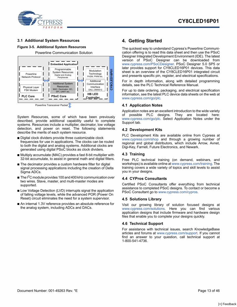
3.1 Additional System ResourcesFigure 3-5. Additional System Resources
System Resources, some of which have been previouslydescribed, provide additional capability useful to completesystems. Resources include a multiplier, decimator, low voltagedetection, and power on reset. The following statementsdescribe the merits of each system resource.■ Digital clock dividers provide three customizable clock
frequencies for use in applications. The clocks can be routed to both the digital and analog systems. Additional clocks are generated using digital PSoC blocks as clock dividers.
■ Multiply accumulate (MAC) provides a fast 8-bit multiplier with 32-bit accumulate, to assist in general math and digital filters.
■ The decimator provides a custom hardware filter for digital signal processing applications including the creation of Delta Sigma ADCs.
■ The I2C module provides 100 and 400 kHz communication over two wires. Slave, master, and multi-master modes are supported.
■ Low Voltage Detection (LVD) interrupts signal the application of falling voltage levels, while the advanced POR (Power On Reset) circuit eliminates the need for a system supervisor.
■ An internal 1.3V reference provides an absolute reference for the analog system, including ADCs and DACs.
4. Getting StartedThe quickest way to understand Cypress’s Powerline Communi-cation offering is to read this data sheet and then use the PSoCDesigner Integrated Development Environment (IDE). The latestversion of PSoC Designer can be downloaded fromwww.cypress.com/PSoCDesigner. PSoC Designer 5.0 SP5 orlater provides support for CY8CLED16P01 devices. This datasheet is an overview of the CY8CLED16P01 integrated circuitand presents specific pin, register, and electrical specifications. For in depth information, along with detailed programmingdetails, see the PLC Technical Reference Manual.For up to date ordering, packaging, and electrical specificationinformation, see the latest PLC device data sheets on the web atwww.cypress.com/go/plc.
4.1 Application NotesApplication notes are an excellent introduction to the wide varietyof possible PLC designs. They are located here:www.cypress.com/go/plc. Select Application Notes under theSupport tab.
4.2 Development KitsPLC Development Kits are available online from Cypress atwww.cypress.com/shop and through a growing number ofregional and global distributors, which include Arrow, Avnet,Digi-Key, Farnell, Future Electronics, and Newark.
4.3 TrainingFree PLC technical training (on demand, webinars, andworkshops) is available online at www.cypress.com/training. Thetraining covers a wide variety of topics and skill levels to assistyou in your designs.
4.4 CYPros ConsultantsCertified PSoC Consultants offer everything from technicalassistance to completed PSoC designs. To contact or become aPSoC Consultant go to www.cypress.com/cypros.
4.5 Solutions LibraryVisit our growing library of solution focused designs atwww.cypress.com/solutions. Here you can find variousapplication designs that include firmware and hardware designfiles that enable you to complete your designs quickly.
4.6 Technical SupportFor assistance with technical issues, search KnowledgeBasearticles and forums at www.cypress.com/support. If you cannotfind an answer to your question, call technical support at1-800-541-4736.
CY8
CLE
D16
P01
Powerline Network Protocol
Physical Layer FSK Modem
Powerline Communication Solution
Powerline Transceiver Packet
Programmable System Resources
Digital and Analog Peripherals
PSoC Core
Additional System Resources
MAC, Decimator, I2C, SPI, UART etc.
PLC Core
Embedded Application
Modulation Technology
PrISM, PWM etc.
Additional Communication
InterfaceDALI, DMX512
HB LED Controller
[+] Feedback [+] Feedback
CY8CLED16P01
Document Number: 001-49263 Rev. *E Page 14 of 46
5. Development ToolsPSoC Designer is a Microsoft® Windows-based, integrateddevelopment environment for the ProgrammableSystem-on-Chip (PSoC) devices. The PSoC Designer IDE runson Windows XP or Windows Vista. This system provides design database management by project,an integrated debugger with In-Circuit Emulator, in-systemprogramming support, and built in support for third partyassemblers and C compilers. PSoC Designer also supports C language compilers developedspecifically for the devices in the PSoC family.
5.1 PSoC Designer Software Subsystems
5.1.1 System-Level ViewA drag-and-drop visual embedded system design environmentbased on PSoC Express. In the system level view you create amodel of your system inputs, outputs, and communicationinterfaces. You define when and how an output device changesstate based upon any or all other system devices. Based uponthe design, PSoC Designer automatically selects one or morePSoC Programmable System-on-Chip Controllers that matchyour system requirements.PSoC Designer generates all embedded code, then compilesand links it into a programming file for a specific PSoC device.
5.1.2 Chip-Level ViewThe chip-level view is a more traditional integrated developmentenvironment (IDE) based on PSoC Designer 4.4. Choose a basedevice to work with and then select different onboard analog anddigital components called user modules that use the PSoCblocks. Examples of user modules are ADCs, DACs, Amplifiers,and Filters. Configure the user modules for your chosenapplication and connect them to each other and to the properpins. Then generate your project. This prepopulates your projectwith APIs and libraries that you can use to program yourapplication.The device editor also supports easy development of multipleconfigurations and dynamic reconfiguration. Dynamicconfiguration allows for changing configurations at run time.
5.1.3 Hybrid DesignsYou can begin in the system-level view, allow it to choose andconfigure your user modules, routing, and generate code, thenswitch to the chip-level view to gain complete control overon-chip resources. All views of the project share a common codeeditor, builder, and common debug, emulation, and programmingtools.
5.1.4 Code Generation ToolsPSoC Designer supports multiple third party C compilers andassemblers. The code generation tools work seamlessly withinthe PSoC Designer interface and have been tested with a fullrange of debugging tools. The choice is yours.
Assemblers. The assemblers allow assembly code to mergeseamlessly with C code. Link libraries automatically use absoluteaddressing or are compiled in relative mode, and linked withother software modules to get absolute addressing.
C Language Compilers. C language compilers are availablethat support the PSoC family of devices. The products allow youto create complete C programs for the PSoC family devices.The optimizing C compilers provide all the features of C tailoredto the PSoC architecture. They come complete with embeddedlibraries providing port and bus operations, standard keypad anddisplay support, and extended math functionality.
5.1.5 DebuggerThe PSoC Designer Debugger subsystem provides hardwarein-circuit emulation, allowing you to test the program in a physicalsystem while providing an internal view of the PSoC device.Debugger commands allow the designer to read and programand read and write data memory, read and write IO registers,read and write CPU registers, set and clear breakpoints, andprovide program run, halt, and step control. The debugger alsoallows the designer to create a trace buffer of registers andmemory locations of interest.
5.1.6 Online Help SystemThe online help system displays online, context-sensitive helpfor the user. Designed for procedural and quick reference, eachfunctional subsystem has its own context-sensitive help. Thissystem also provides tutorials and links to FAQs and an OnlineSupport Forum to aid the designer in getting started.
5.2 In-Circuit Emulator (ICE)A low cost, high functionality In-Circuit Emulator (ICE) isavailable for development support. This hardware has thecapability to program single devices.The emulator consists of a base unit that connects to the PC byway of a USB port. The base unit is universal and operates withall PSoC devices. Emulation pods for each device family areavailable separately. The emulation pod takes the place of thePSoC device in the target board and performs full speed (24MHz) operation.
[+] Feedback [+] Feedback
CY8CLED16P01
Document Number: 001-49263 Rev. *E Page 15 of 46
6. Designing with User ModulesThe development process for the PSoC device differs from thatof a traditional fixed function microprocessor. The configurableanalog and digital hardware blocks give the PSoC architecture aunique flexibility that pays dividends in managing specificationchange during development and by lowering inventory costs.These configurable resources, called PSoC Blocks, have theability to implement a wide variety of user selectable functions. The PSoC development process can be summarized in thefollowing four steps: 1. Select Components2. Configure Components3. Organize and Connect4. Generate, Verify, and Debug
6.1 Select ComponentsBoth the system-level and chip-level views provide a library ofprebuilt, pretested hardware peripheral components. In thesystem-level view, these components are called “drivers” andcorrespond to inputs (a thermistor, for example), outputs (abrushless DC fan, for example), communication interfaces(I2C-bus, for example), and the logic to control how they interactwith one another (called valuators). In the chip-level view, the components are called “user modules”.User modules make selecting and implementing peripheraldevices simple, and come in analog, digital, and programmablesystem-on-chip varieties.
6.2 Configure ComponentsEach of the components you select establishes the basic registersettings that implement the selected function. They also provideparameters and properties that allow you to tailor their preciseconfiguration to your particular application. For example, a PulseWidth Modulator (PWM) User Module configures one or moredigital PSoC blocks, one for each 8 bits of resolution. The usermodule parameters permit you to establish the pulse width andduty cycle. Configure the parameters and properties tocorrespond to your chosen application. Enter values directly orby selecting values from drop-down menus.Both the system-level drivers and chip-level user modules aredocumented in data sheets that are viewed directly in the PSoCDesigner. These data sheets explain the internal operation of thecomponent and provide performance specifications. Each datasheet describes the use of each user module parameter or driver
property, and other information you may need to successfullyimplement your design.
6.3 Organize and ConnectYou can build signal chains at the chip level by interconnectinguser modules to each other and the IO pins, or connect systemlevel inputs, outputs, and communication interfaces to eachother with valuator functions.In the system-level view, selecting a potentiometer driver tocontrol a variable speed fan driver and setting up the valuatorsto control the fan speed based on input from the pot selects,places, routes, and configures a programmable gain amplifier(PGA) to buffer the input from the potentiometer, an analog todigital converter (ADC) to convert the potentiometer’s output toa digital signal, and a PWM to control the fan. In the chip-level view, perform the selection, configuration, androuting so that you have complete control over the use of allon-chip resources.
6.4 Generate, Verify, and DebugWhen you are ready to test the hardware configuration or moveon to developing code for the project, perform the “GenerateApplication” step. This causes PSoC Designer to generatesource code that automatically configures the device to yourspecification and provides the software for the system.Both system-level and chip-level designs generate softwarebased on your design. The chip-level design provides applicationprogramming interfaces (APIs) with high level functions tocontrol and respond to hardware events at run time and interruptservice routines that you can adapt as needed. The system-leveldesign also generates a C main() program that completelycontrols the chosen application and contains placeholders forcustom code at strategic positions allowing you to further refinethe software without disrupting the generated code.A complete code development environment allows you todevelop and customize your applications in C, assemblylanguage, or both.The last step in the development process takes place inside thePSoC Designer’s Debugger subsystem. The Debuggerdownloads the HEX image to the ICE where it runs at full speed.Debugger capabilities rival those of systems costing many timesmore. In addition to traditional single-step, run-to-breakpoint andwatch-variable features, the Debugger provides a large tracebuffer and allows you define complex breakpoint events thatinclude monitoring address and data bus values, memorylocations and external signals.
[+] Feedback [+] Feedback
CY8CLED16P01
Document Number: 001-49263 Rev. *E Page 16 of 46
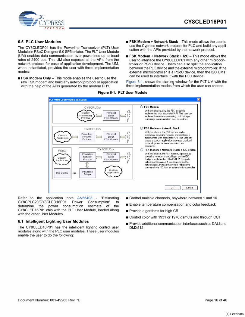
6.5 PLC User ModulesThe CY8CLEDP01 has the Powerline Transceiver (PLT) UserModule in PSoC Designer 5.0 SP5 or later. The PLT User Module(UM) enables data communication over powerlines up to baudrates of 2400 bps. This UM also exposes all the APIs from thenetwork protocol for ease of application development. The UM,when instantiated, provides the user with three implementationmodes:
■ FSK Modem Only – This mode enables the user to use the raw FSK modem and build any network protocol or application with the help of the APIs generated by the modem PHY.
■ FSK Modem + Network Stack – This mode allows the user to use the Cypress network protocol for PLC and build any appli-cation with the APIs provided by the network protocol.
■ FSK Modem + Network Stack + I2C – This mode allows the user to interface the CY8CLEDP01 with any other microcon-troller or PSoC device. Users can also split the application between the PLC device and the external microcontroller. If the external microcontroller is a PSoC device, then the I2C UMs can be used to interface it with the PLC device.
Figure 6-1. shows the starting window for the PLT UM with thethree implementation modes from which the user can choose.
Figure 6-1. PLT User Module
Refer to the application note AN55403 - "EstimatingCY8CPLC20/CY8CLED16P01 Power Consumption" todetermine the power consumption estimate of theCY8CLED16P01 chip with the PLT User Module, loaded alongwith the other User Modules.
6.1 Intelligent Lighting User ModulesThe CY8CLED16P01 has the intelligent lighting control usermodules along with the PLC user modules. These user modulesenable the user to do the following:
■ Control multiple channels, anywhere between 1 and 16.
■ Enable temperature compensation and color feedback
■ Provide algorithms for high CRI
■ Control color with 1931 or 1976 gamuts and through CCT
■ Provide additional communication interfaces such as DALI and DMX512
[+] Feedback [+] Feedback
CY8CLED16P01
Document Number: 001-49263 Rev. *E Page 17 of 46
7. Document Conventions7.1 Acronyms UsedThis table lists the acronyms used in this data sheet.
7.2 Units of MeasureA units of measure table is located in the section ElectricalSpecifications on page 25.
7.3 Numeric NamingHexadecimal numbers are represented with all letters inuppercase with an appended lowercase ‘h’ (for example, ‘14h’ or‘3Ah’). Hexadecimal numbers may also be represented by a ‘0x’prefix, the C coding convention. Binary numbers have anappended lowercase ‘b’ (for example, 01010100b’ or‘01000011b’). Numbers not indicated by an ‘h’, ‘b’, or 0x aredecimal.
Table 7-1. Acronyms
Acronym DescriptionAC alternating currentADC analog-to-digital converterAPI application programming interfaceCPU central processing unitCT continuous timeDAC digital-to-analog converterDC direct currentEEPROM electrically erasable programmable read-only
memoryFSR full scale rangeGPIO general purpose IOICE in-circuit emulatorIDE integrated development environment IO input/outputISSP in-system serial programmingIPOR imprecise power on resetLSb least-significant bitLVD low voltage detectMSb most-significant bitPC program counterPGA programmable gain amplifierPOR power on resetPPOR precision power on resetPSoC® Programmable System-on-ChipPWM pulse width modulatorROM read only memorySC switched capacitorSRAM static random access memory
[+] Feedback [+] Feedback
CY8CLED16P01
Document Number: 001-49263 Rev. *E Page 18 of 46
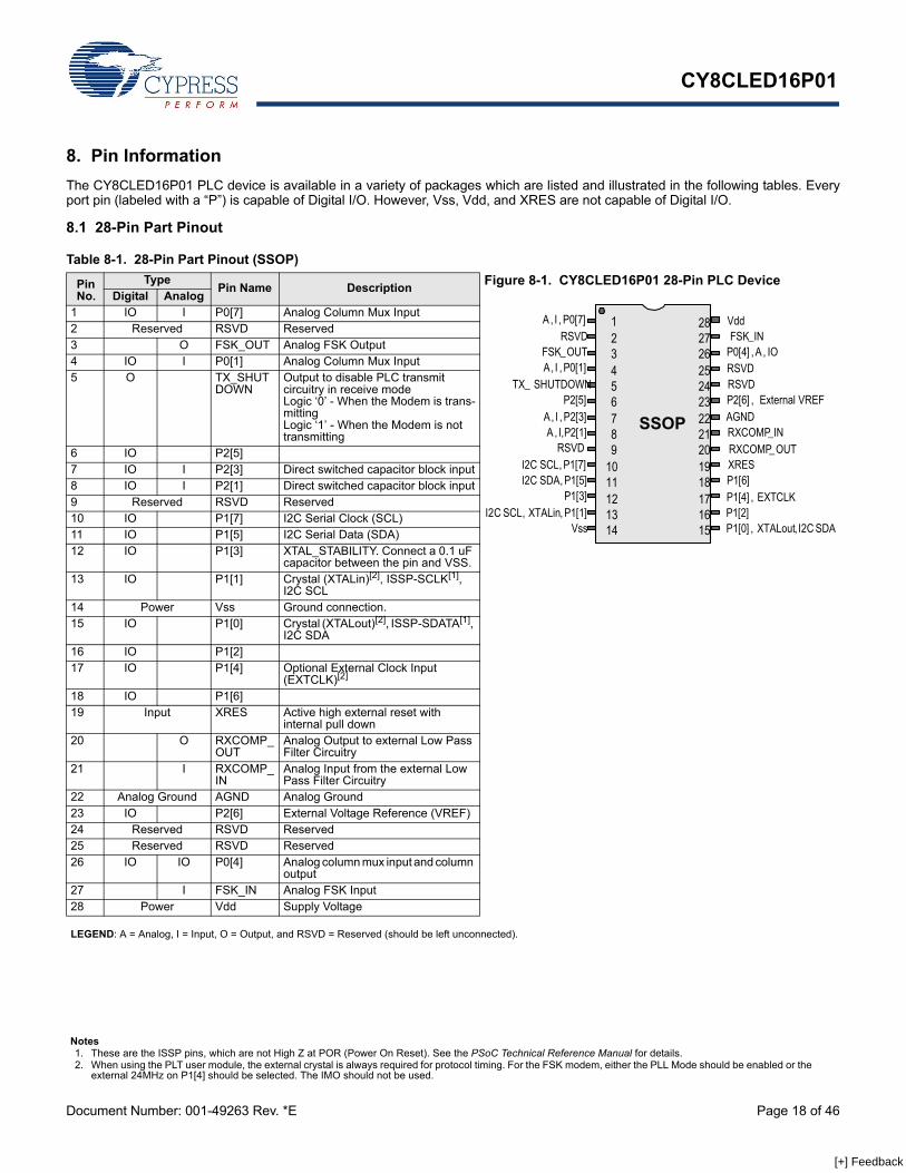
8. Pin InformationThe CY8CLED16P01 PLC device is available in a variety of packages which are listed and illustrated in the following tables. Everyport pin (labeled with a “P”) is capable of Digital I/O. However, Vss, Vdd, and XRES are not capable of Digital I/O.
8.1 28-Pin Part Pinout
Table 8-1. 28-Pin Part Pinout (SSOP)
Pin No.
Type Pin Name Description Figure 8-1. CY8CLED16P01 28-Pin PLC Device Digital Analog
1 IO I P0[7] Analog Column Mux Input2 Reserved RSVD Reserved3 O FSK_OUT Analog FSK Output4 IO I P0[1] Analog Column Mux Input5 O TX_SHUT
DOWNOutput to disable PLC transmit circuitry in receive modeLogic ‘0’ - When the Modem is trans-mittingLogic ‘1’ - When the Modem is not transmitting
6 IO P2[5]7 IO I P2[3] Direct switched capacitor block input8 IO I P2[1] Direct switched capacitor block input9 Reserved RSVD Reserved10 IO P1[7] I2C Serial Clock (SCL)11 IO P1[5] I2C Serial Data (SDA)12 IO P1[3] XTAL_STABILITY. Connect a 0.1 uF
capacitor between the pin and VSS.13 IO P1[1] Crystal (XTALin)[2], ISSP-SCLK[1],
I2C SCL14 Power Vss Ground connection.15 IO P1[0] Crystal (XTALout)[2], ISSP-SDATA[1],
I2C SDA16 IO P1[2]17 IO P1[4] Optional External Clock Input
(EXTCLK)[2]
18 IO P1[6] 19 Input XRES Active high external reset with
internal pull down20 O RXCOMP_
OUTAnalog Output to external Low Pass Filter Circuitry
21 I RXCOMP_IN
Analog Input from the external Low Pass Filter Circuitry
22 Analog Ground AGND Analog Ground23 IO P2[6] External Voltage Reference (VREF)24 Reserved RSVD Reserved25 Reserved RSVD Reserved26 IO IO P0[4] Analog column mux input and column
output27 I FSK_IN Analog FSK Input28 Power Vdd Supply Voltage
LEGEND: A = Analog, I = Input, O = Output, and RSVD = Reserved (should be left unconnected).
Notes1. These are the ISSP pins, which are not High Z at POR (Power On Reset). See the PSoC Technical Reference Manual for details.2. When using the PLT user module, the external crystal is always required for protocol timing. For the FSK modem, either the PLL Mode should be enabled or the
external 24MHz on P1[4] should be selected. The IMO should not be used.
A, I , P0[7]RSVD
FSK_OUTA, I , P0[1]
TX_ SHUTDOWNP2[5]
A, I , P2[3]A , I,P2[1]
RSVDI2C SCL, P1[7]I2C SDA, P1[5]
P1[3]I2C SCL, XTALin, P1[1]
Vss
VddFSK_IN
P0[4] , A , IORSVDRSVDP2[6] , External VREFAGNDRXCOMP_INRXCOMP_OUTXRESP1[6]P1[4] , EXTCLKP1[2]P1[0] , XTALout, I2C SDA
SSOP
123456789
1011121314
2827262524232221201918171615
[+] Feedback
CY8CLED16P01
Document Number: 001-49263 Rev. *E Page 19 of 46
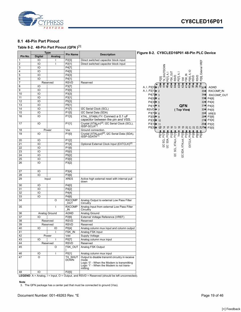
8.1 48-Pin Part PinoutTable 8-2. 48-Pin Part Pinout (QFN )[3]
Pin No.Type Pin Name Description Figure 8-2. CY8CLED16P01 48-Pin PLC Device
Digital Analog1 IO I P2[3] Direct switched capacitor block input2 IO I P2[1] Direct switched capacitor block input3 IO P4[7]4 IO P4[5]5 IO P4[3]6 IO P4[1]7 Reserved RSVD Reserved8 IO P3[7]9 IO P3[5]10 IO P3[3]11 IO P3[1]12 IO P5[3]13 IO P5[1]14 IO P1[7] I2C Serial Clock (SCL)15 IO P1[5] I2C Serial Data (SDA)16 IO P1[3] XTAL_STABILITY. Connect a 0.1 uF
capacitor between the pin and VSS.17 IO P1[1] Crystal (XTALin)[2], I2C Serial Clock (SCL),
ISSP-SCLK[1]
18 Power Vss Ground connection.19 IO P1[0] Crystal (XTALout)[2], I2C Serial Data (SDA),
ISSP-SDATA[1]
20 IO P1[2]21 IO P1[4] Optional External Clock Input (EXTCLK)[2]
22 IO P1[6]23 IO P5[0]24 IO P5[2]25 IO P3[0]26 IO P3[2]
27 IO P3[4]28 IO P3[6]29 Input XRES Active high external reset with internal pull
down30 IO P4[0]31 IO P4[2]32 IO P4[4]33 IO P4[6]34 O RXCOMP
_OUTAnalog Output to external Low Pass Filter Circuitry
35 I RXCOMP_IN
Analog Input from external Low Pass Filter Circuitry
36 Analog Ground AGND Analog Ground37 IO P2[6] External Voltage Reference (VREF)38 Reserved RSVD Reserved39 Reserved RSVD Reserved40 IO IO P0[4] Analog column mux input and column output41 I FSK_IN Analog FSK Input42 Power Vdd Supply Voltage43 IO I P0[7] Analog column mux input44 Reserved RSVD Reserved 45 O FSK_OUT
]Analog FSK Output
46 IO I P0[1] Analog column mux input47 O TX_SHUT
DOWNOutput to disable transmit circuitry in receive modeLogic ‘0’ - When the Modem is transmittingLogic ‘1’ - When the Modem is not trans-mitting
48 IO P2[5]LEGEND: A = Analog, I = Input, O = Output, and RSVD = Reserved (should be left unconnected).
Note3. The QFN package has a center pad that must be connected to ground (Vss).
QFN( Top View)
P2[5]
TX_S
HUTD
OWN
P0[1]
,A,I
FSK_
OUT
RSVD
P0[7]
,A,I
Vdd
FSK_
INP0
[4],A
,IO
RSVD
RSVD
P2[6]
,Exte
rnal
VREF
101112
A, I , P2[3]A , I , P2[1]
P4[7]P4[5]P4[3]P4[1]
RSVDP3[7]P3[5]P3[3]P3[1]P5[3]
3534333231302928272625
3648 4 7 4 6 45 44 43 42 41 40 39 38 3 7
RXCOMP_INRXCOMP_OUT
P4[6]P4[4]P4[2]P4[0]XRESP3[6]P3[4]P3[2]P3[0]
AGND123456789
13 14 15 16 17 18 19 20 21 22 23 24
P5[1]
I2C
SCL,
P1[7]
I2C
SDA,
P1[5]
P1[3]
I2C
SCL,
XTAL
in,P1
[1] Vss
I2C
SDA,
XTAL
out,
P1[0]
P1[2]
EXTC
LK,P
1[4]
P1[6]
P5[0]
P5[2]
[+] Feedback
CY8CLED16P01
Document Number: 001-49263 Rev. *E Page 20 of 46
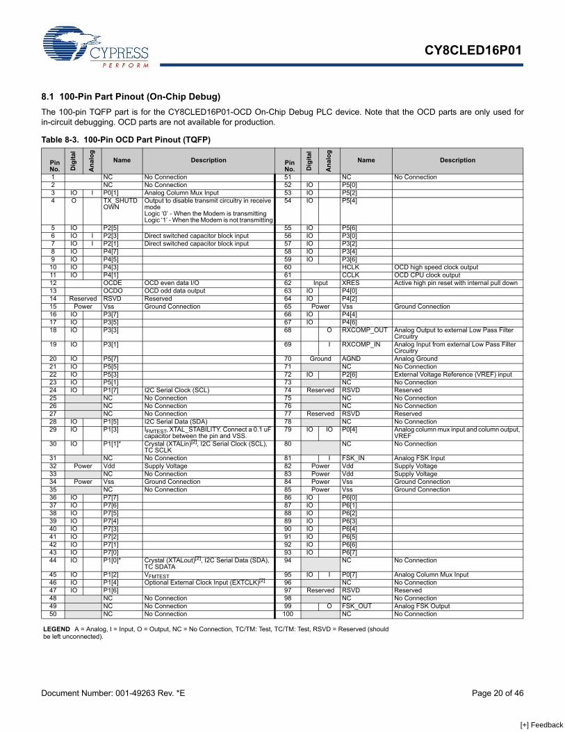
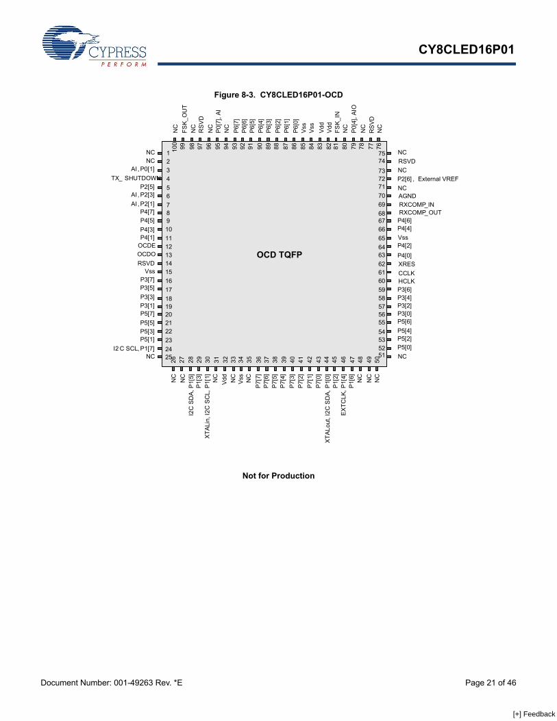
8.1 100-Pin Part Pinout (On-Chip Debug)The 100-pin TQFP part is for the CY8CLED16P01-OCD On-Chip Debug PLC device. Note that the OCD parts are only used forin-circuit debugging. OCD parts are not available for production.
Table 8-3. 100-Pin OCD Part Pinout (TQFP)
Pin No. D
igita
l
Ana
log
Name Description Pin No. D
igita
l
Ana
log
Name Description
1 NC No Connection 51 NC No Connection2 NC No Connection 52 IO P5[0]3 IO I P0[1] Analog Column Mux Input 53 IO P5[2]4 O TX_SHUTD
OWNOutput to disable transmit circuitry in receive modeLogic ‘0’ - When the Modem is transmittingLogic ‘1’ - When the Modem is not transmitting
54 IO P5[4]
5 IO P2[5] 55 IO P5[6]6 IO I P2[3] Direct switched capacitor block input 56 IO P3[0]7 IO I P2[1] Direct switched capacitor block input 57 IO P3[2]8 IO P4[7] 58 IO P3[4]9 IO P4[5] 59 IO P3[6]
10 IO P4[3] 60 HCLK OCD high speed clock output11 IO P4[1] 61 CCLK OCD CPU clock output12 OCDE OCD even data I/O 62 Input XRES Active high pin reset with internal pull down13 OCDO OCD odd data output 63 IO P4[0]14 Reserved RSVD Reserved 64 IO P4[2]15 Power Vss Ground Connection 65 Power Vss Ground Connection16 IO P3[7] 66 IO P4[4]17 IO P3[5] 67 IO P4[6]18 IO P3[3] 68 O RXCOMP_OUT Analog Output to external Low Pass Filter
Circuitry19 IO P3[1] 69 I RXCOMP_IN Analog Input from external Low Pass Filter
Circuitry20 IO P5[7] 70 Ground AGND Analog Ground21 IO P5[5] 71 NC No Connection22 IO P5[3] 72 IO P2[6] External Voltage Reference (VREF) input23 IO P5[1] 73 NC No Connection24 IO P1[7] I2C Serial Clock (SCL) 74 Reserved RSVD Reserved25 NC No Connection 75 NC No Connection26 NC No Connection 76 NC No Connection27 NC No Connection 77 Reserved RSVD Reserved28 IO P1[5] I2C Serial Data (SDA) 78 NC No Connection29 IO P1[3] IFMTEST, XTAL_STABILITY. Connect a 0.1 uF
capacitor between the pin and VSS.79 IO IO P0[4] Analog column mux input and column output,
VREF30 IO P1[1]* Crystal (XTALin)[2], I2C Serial Clock (SCL),
TC SCLK80 NC No Connection
31 NC No Connection 81 I FSK_IN Analog FSK Input32 Power Vdd Supply Voltage 82 Power Vdd Supply Voltage33 NC No Connection 83 Power Vdd Supply Voltage34 Power Vss Ground Connection 84 Power Vss Ground Connection35 NC No Connection 85 Power Vss Ground Connection36 IO P7[7] 86 IO P6[0]37 IO P7[6] 87 IO P6[1]38 IO P7[5] 88 IO P6[2]39 IO P7[4] 89 IO P6[3]40 IO P7[3] 90 IO P6[4]41 IO P7[2] 91 IO P6[5]42 IO P7[1] 92 IO P6[6]43 IO P7[0] 93 IO P6[7]44 IO P1[0]* Crystal (XTALout)[2], I2C Serial Data (SDA),
TC SDATA94 NC No Connection
45 IO P1[2] VFMTEST 95 IO I P0[7] Analog Column Mux Input46 IO P1[4] Optional External Clock Input (EXTCLK)[2] 96 NC No Connection47 IO P1[6] 97 Reserved RSVD Reserved48 NC No Connection 98 NC No Connection49 NC No Connection 99 O FSK_OUT Analog FSK Output50 NC No Connection 100 NC No Connection
LEGEND A = Analog, I = Input, O = Output, NC = No Connection, TC/TM: Test, TC/TM: Test, RSVD = Reserved (should be left unconnected).
[+] Feedback
CY8CLED16P01
Document Number: 001-49263 Rev. *E Page 21 of 46
Figure 8-3. CY8CLED16P01-OCD
Not for Production
OCD TQFP
100
99 98 97 96 95 94 93 92 91 90 89 88 87 86 85 84 83 82 81 80 79 78 77 76
10111213141516171819202122232425
123456789
NCNC
AI, P0[1]TX_ SHUTDOWN
P2[5]AI , P2[3]AI , P2[1]
P4[7]P4[5]P4[3]P4[1]
OCDEOCDORSVD
VssP3[7]P3[5]P3[3]P3[1]P5[7]P5[5]P5[3]P5[1]
I2 C SCL, P1[7]NC
26 27 28 29 30 31 32 33 34 35 36 37 38 39 40 41 42 43 44 45 46 47 48 5049
NC
Vss
P7[3
]
EX
TCLK
, P1[
4]NC
I2C
SD
A, P
1[5]
P1[3
]X
TALi
n, I2
C S
CL,
P1[
1] NC
Vdd
NC
NC
P7[7
]P7
[6]
P7[5
]P7
[4]
P7[2
]P7
[1]
P7[0
]X
TALo
ut, I
2C S
DA,
P1[
0]P1
[2]
P1[6
]N
CN
CN
C
75747372717069686766656463626160595857565554535251
NCRSVDNCP2[6] , External VREFNCAGNDRXCOMP_INRXCOMP_OUTP4[6]P4[4]VssP4[2]P4[0]XRESCCLKHCLKP3[6]P3[4]P3[2]P3[0]P5[6]P5[4]P5[2]P5[0]NC
NC
FSK_
OU
TN
CR
SV
DN
CP
0[7]
, AI
NC
P6[
7]P
6[6]
P6[
5]P
6[4]
P6[
3]P
6[2]
P6[
1]P
6[0]
Vss
Vss
Vdd
Vdd
FSK_
INN
CP
0[4]
, AIO
NC
RS
VDN
C
[+] Feedback
CY8CLED16P01
Document Number: 001-49263 Rev. *E Page 22 of 46
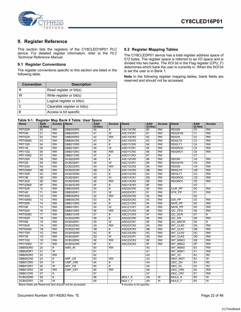
9. Register ReferenceThis section lists the registers of the CY8CLED16P01 PLCdevice. For detailed register information, refer to the PLCTechnical Reference Manual.
9.1 Register ConventionsThe register conventions specific to this section are listed in thefollowing table.
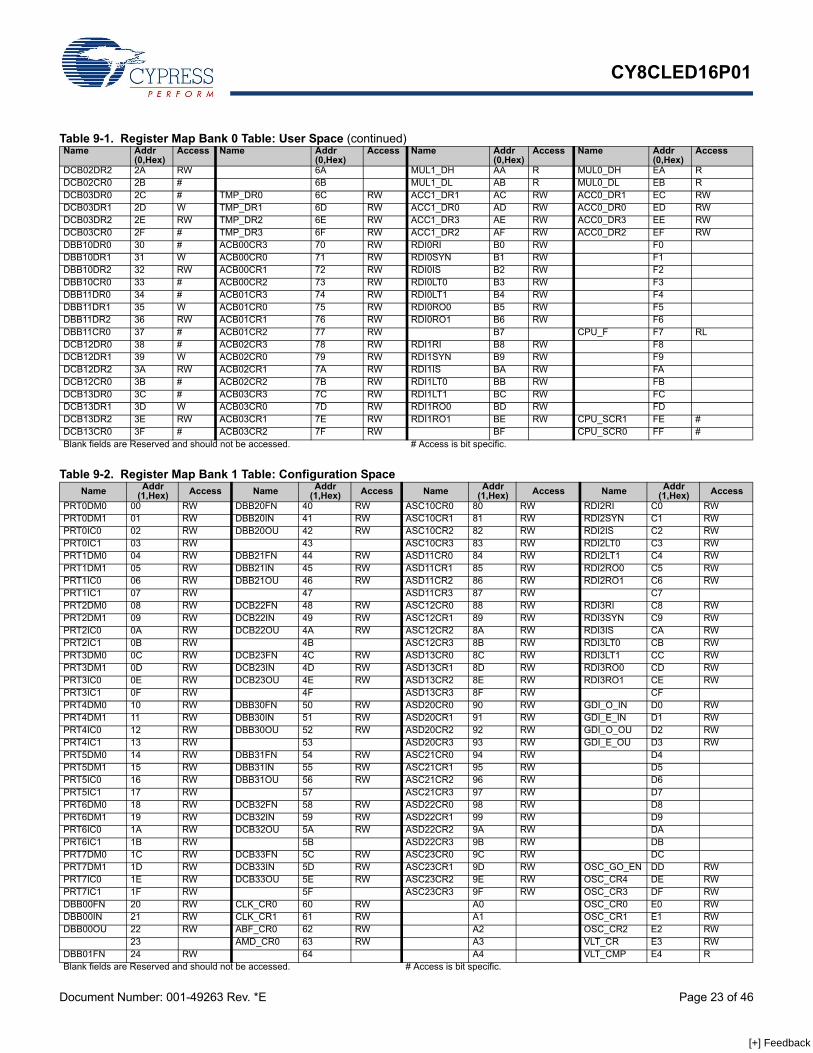
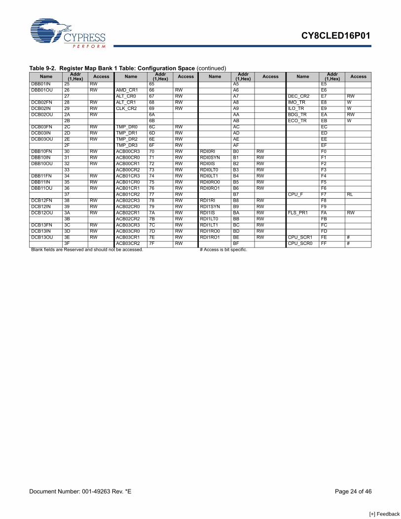
9.2 Register Mapping TablesThe CY8CLEDP01 device has a total register address space of512 bytes. The register space is referred to as I/O space and isdivided into two banks. The XOI bit in the Flag register (CPU_F)determines which bank the user is currently in. When the XOI bitis set the user is in Bank 1.Note In the following register mapping tables, blank fields arereserved and should not be accessed.
Convention DescriptionR Read register or bit(s)W Write register or bit(s)L Logical register or bit(s)C Clearable register or bit(s)# Access is bit specific
Table 9-1. Register Map Bank 0 Table: User SpaceName Addr
(0,Hex)Access Name Addr
(0,Hex)Access Name Addr
(0,Hex)Access Name Addr
(0,Hex)Access
PRT0DR 00 RW DBB20DR0 40 # ASC10CR0 80 RW RDI2RI C0 RWPRT0IE 01 RW DBB20DR1 41 W ASC10CR1 81 RW RDI2SYN C1 RWPRT0GS 02 RW DBB20DR2 42 RW ASC10CR2 82 RW RDI2IS C2 RWPRT0DM2 03 RW DBB20CR0 43 # ASC10CR3 83 RW RDI2LT0 C3 RWPRT1DR 04 RW DBB21DR0 44 # ASD11CR0 84 RW RDI2LT1 C4 RWPRT1IE 05 RW DBB21DR1 45 W ASD11CR1 85 RW RDI2RO0 C5 RWPRT1GS 06 RW DBB21DR2 46 RW ASD11CR2 86 RW RDI2RO1 C6 RWPRT1DM2 07 RW DBB21CR0 47 # ASD11CR3 87 RW C7PRT2DR 08 RW DCB22DR0 48 # ASC12CR0 88 RW RDI3RI C8 RWPRT2IE 09 RW DCB22DR1 49 W ASC12CR1 89 RW RDI3SYN C9 RWPRT2GS 0A RW DCB22DR2 4A RW ASC12CR2 8A RW RDI3IS CA RWPRT2DM2 0B RW DCB22CR0 4B # ASC12CR3 8B RW RDI3LT0 CB RWPRT3DR 0C RW DCB23DR0 4C # ASD13CR0 8C RW RDI3LT1 CC RWPRT3IE 0D RW DCB23DR1 4D W ASD13CR1 8D RW RDI3RO0 CD RWPRT3GS 0E RW DCB23DR2 4E RW ASD13CR2 8E RW RDI3RO1 CE RWPRT3DM2 0F RW DCB23CR0 4F # ASD13CR3 8F RW CFPRT4DR 10 RW DBB30DR0 50 # ASD20CR0 90 RW CUR_PP D0 RWPRT4IE 11 RW DBB30DR1 51 W ASD20CR1 91 RW STK_PP D1 RWPRT4GS 12 RW DBB30DR2 52 RW ASD20CR2 92 RW D2PRT4DM2 13 RW DBB30CR0 53 # ASD20CR3 93 RW IDX_PP D3 RWPRT5DR 14 RW DBB31DR0 54 # ASC21CR0 94 RW MVR_PP D4 RWPRT5IE 15 RW DBB31DR1 55 W ASC21CR1 95 RW MVW_PP D5 RWPRT5GS 16 RW DBB31DR2 56 RW ASC21CR2 96 RW I2C_CFG D6 RWPRT5DM2 17 RW DBB31CR0 57 # ASC21CR3 97 RW I2C_SCR D7 #PRT6DR 18 RW DCB32DR0 58 # ASD22CR0 98 RW I2C_DR D8 RWPRT6IE 19 RW DCB32DR1 59 W ASD22CR1 99 RW I2C_MSCR D9 #PRT6GS 1A RW DCB32DR2 5A RW ASD22CR2 9A RW INT_CLR0 DA RWPRT6DM2 1B RW DCB32CR0 5B # ASD22CR3 9B RW INT_CLR1 DB RWPRT7DR 1C RW DCB33DR0 5C # ASC23CR0 9C RW INT_CLR2 DC RWPRT7IE 1D RW DCB33DR1 5D W ASC23CR1 9D RW INT_CLR3 DD RWPRT7GS 1E RW DCB33DR2 5E RW ASC23CR2 9E RW INT_MSK3 DE RWPRT7DM2 1F RW DCB33CR0 5F # ASC23CR3 9F RW INT_MSK2 DF RWDBB00DR0 20 # AMX_IN 60 RW A0 INT_MSK0 E0 RWDBB00DR1 21 W 61 A1 INT_MSK1 E1 RWDBB00DR2 22 RW 62 A2 INT_VC E2 RCDBB00CR0 23 # ARF_CR 63 RW A3 RES_WDT E3 WDBB01DR0 24 # CMP_CR0 64 # A4 DEC_DH E4 RCDBB01DR1 25 W ASY_CR 65 # A5 DEC_DL E5 RCDBB01DR2 26 RW CMP_CR1 66 RW A6 DEC_CR0 E6 RWDBB01CR0 27 # 67 A7 DEC_CR1 E7 RWDCB02DR0 28 # 68 MUL1_X A8 W MUL0_X E8 WDCB02DR1 29 W 69 MUL1_Y A9 W MUL0_Y E9 WBlank fields are Reserved and should not be accessed. # Access is bit specific.
[+] Feedback
CY8CLED16P01
Document Number: 001-49263 Rev. *E Page 23 of 46
DCB02DR2 2A RW 6A MUL1_DH AA R MUL0_DH EA RDCB02CR0 2B # 6B MUL1_DL AB R MUL0_DL EB RDCB03DR0 2C # TMP_DR0 6C RW ACC1_DR1 AC RW ACC0_DR1 EC RWDCB03DR1 2D W TMP_DR1 6D RW ACC1_DR0 AD RW ACC0_DR0 ED RWDCB03DR2 2E RW TMP_DR2 6E RW ACC1_DR3 AE RW ACC0_DR3 EE RWDCB03CR0 2F # TMP_DR3 6F RW ACC1_DR2 AF RW ACC0_DR2 EF RWDBB10DR0 30 # ACB00CR3 70 RW RDI0RI B0 RW F0DBB10DR1 31 W ACB00CR0 71 RW RDI0SYN B1 RW F1DBB10DR2 32 RW ACB00CR1 72 RW RDI0IS B2 RW F2DBB10CR0 33 # ACB00CR2 73 RW RDI0LT0 B3 RW F3DBB11DR0 34 # ACB01CR3 74 RW RDI0LT1 B4 RW F4DBB11DR1 35 W ACB01CR0 75 RW RDI0RO0 B5 RW F5DBB11DR2 36 RW ACB01CR1 76 RW RDI0RO1 B6 RW F6DBB11CR0 37 # ACB01CR2 77 RW B7 CPU_F F7 RLDCB12DR0 38 # ACB02CR3 78 RW RDI1RI B8 RW F8DCB12DR1 39 W ACB02CR0 79 RW RDI1SYN B9 RW F9DCB12DR2 3A RW ACB02CR1 7A RW RDI1IS BA RW FADCB12CR0 3B # ACB02CR2 7B RW RDI1LT0 BB RW FBDCB13DR0 3C # ACB03CR3 7C RW RDI1LT1 BC RW FCDCB13DR1 3D W ACB03CR0 7D RW RDI1RO0 BD RW FDDCB13DR2 3E RW ACB03CR1 7E RW RDI1RO1 BE RW CPU_SCR1 FE #DCB13CR0 3F # ACB03CR2 7F RW BF CPU_SCR0 FF #
Table 9-1. Register Map Bank 0 Table: User Space (continued)Name Addr
(0,Hex)Access Name Addr
(0,Hex)Access Name Addr
(0,Hex)Access Name Addr
(0,Hex)Access
Blank fields are Reserved and should not be accessed. # Access is bit specific.
Table 9-2. Register Map Bank 1 Table: Configuration SpaceName Addr
(1,Hex) Access Name Addr (1,Hex) Access Name Addr
(1,Hex) Access Name Addr (1,Hex) Access
PRT0DM0 00 RW DBB20FN 40 RW ASC10CR0 80 RW RDI2RI C0 RWPRT0DM1 01 RW DBB20IN 41 RW ASC10CR1 81 RW RDI2SYN C1 RWPRT0IC0 02 RW DBB20OU 42 RW ASC10CR2 82 RW RDI2IS C2 RWPRT0IC1 03 RW 43 ASC10CR3 83 RW RDI2LT0 C3 RWPRT1DM0 04 RW DBB21FN 44 RW ASD11CR0 84 RW RDI2LT1 C4 RWPRT1DM1 05 RW DBB21IN 45 RW ASD11CR1 85 RW RDI2RO0 C5 RWPRT1IC0 06 RW DBB21OU 46 RW ASD11CR2 86 RW RDI2RO1 C6 RWPRT1IC1 07 RW 47 ASD11CR3 87 RW C7PRT2DM0 08 RW DCB22FN 48 RW ASC12CR0 88 RW RDI3RI C8 RWPRT2DM1 09 RW DCB22IN 49 RW ASC12CR1 89 RW RDI3SYN C9 RWPRT2IC0 0A RW DCB22OU 4A RW ASC12CR2 8A RW RDI3IS CA RWPRT2IC1 0B RW 4B ASC12CR3 8B RW RDI3LT0 CB RWPRT3DM0 0C RW DCB23FN 4C RW ASD13CR0 8C RW RDI3LT1 CC RWPRT3DM1 0D RW DCB23IN 4D RW ASD13CR1 8D RW RDI3RO0 CD RWPRT3IC0 0E RW DCB23OU 4E RW ASD13CR2 8E RW RDI3RO1 CE RWPRT3IC1 0F RW 4F ASD13CR3 8F RW CFPRT4DM0 10 RW DBB30FN 50 RW ASD20CR0 90 RW GDI_O_IN D0 RWPRT4DM1 11 RW DBB30IN 51 RW ASD20CR1 91 RW GDI_E_IN D1 RWPRT4IC0 12 RW DBB30OU 52 RW ASD20CR2 92 RW GDI_O_OU D2 RWPRT4IC1 13 RW 53 ASD20CR3 93 RW GDI_E_OU D3 RWPRT5DM0 14 RW DBB31FN 54 RW ASC21CR0 94 RW D4PRT5DM1 15 RW DBB31IN 55 RW ASC21CR1 95 RW D5PRT5IC0 16 RW DBB31OU 56 RW ASC21CR2 96 RW D6PRT5IC1 17 RW 57 ASC21CR3 97 RW D7PRT6DM0 18 RW DCB32FN 58 RW ASD22CR0 98 RW D8PRT6DM1 19 RW DCB32IN 59 RW ASD22CR1 99 RW D9PRT6IC0 1A RW DCB32OU 5A RW ASD22CR2 9A RW DAPRT6IC1 1B RW 5B ASD22CR3 9B RW DBPRT7DM0 1C RW DCB33FN 5C RW ASC23CR0 9C RW DCPRT7DM1 1D RW DCB33IN 5D RW ASC23CR1 9D RW OSC_GO_EN DD RWPRT7IC0 1E RW DCB33OU 5E RW ASC23CR2 9E RW OSC_CR4 DE RWPRT7IC1 1F RW 5F ASC23CR3 9F RW OSC_CR3 DF RWDBB00FN 20 RW CLK_CR0 60 RW A0 OSC_CR0 E0 RWDBB00IN 21 RW CLK_CR1 61 RW A1 OSC_CR1 E1 RWDBB00OU 22 RW ABF_CR0 62 RW A2 OSC_CR2 E2 RW
23 AMD_CR0 63 RW A3 VLT_CR E3 RWDBB01FN 24 RW 64 A4 VLT_CMP E4 RBlank fields are Reserved and should not be accessed. # Access is bit specific.
[+] Feedback
CY8CLED16P01
Document Number: 001-49263 Rev. *E Page 24 of 46
DBB01IN 25 RW 65 A5 E5DBB01OU 26 RW AMD_CR1 66 RW A6 E6
27 ALT_CR0 67 RW A7 DEC_CR2 E7 RWDCB02FN 28 RW ALT_CR1 68 RW A8 IMO_TR E8 WDCB02IN 29 RW CLK_CR2 69 RW A9 ILO_TR E9 WDCB02OU 2A RW 6A AA BDG_TR EA RW
2B 6B AB ECO_TR EB WDCB03FN 2C RW TMP_DR0 6C RW AC ECDCB03IN 2D RW TMP_DR1 6D RW AD EDDCB03OU 2E RW TMP_DR2 6E RW AE EE
2F TMP_DR3 6F RW AF EFDBB10FN 30 RW ACB00CR3 70 RW RDI0RI B0 RW F0DBB10IN 31 RW ACB00CR0 71 RW RDI0SYN B1 RW F1DBB10OU 32 RW ACB00CR1 72 RW RDI0IS B2 RW F2
33 ACB00CR2 73 RW RDI0LT0 B3 RW F3DBB11FN 34 RW ACB01CR3 74 RW RDI0LT1 B4 RW F4DBB11IN 35 RW ACB01CR0 75 RW RDI0RO0 B5 RW F5DBB11OU 36 RW ACB01CR1 76 RW RDI0RO1 B6 RW F6
37 ACB01CR2 77 RW B7 CPU_F F7 RLDCB12FN 38 RW ACB02CR3 78 RW RDI1RI B8 RW F8DCB12IN 39 RW ACB02CR0 79 RW RDI1SYN B9 RW F9DCB12OU 3A RW ACB02CR1 7A RW RDI1IS BA RW FLS_PR1 FA RW
3B ACB02CR2 7B RW RDI1LT0 BB RW FBDCB13FN 3C RW ACB03CR3 7C RW RDI1LT1 BC RW FCDCB13IN 3D RW ACB03CR0 7D RW RDI1RO0 BD RW FDDCB13OU 3E RW ACB03CR1 7E RW RDI1RO1 BE RW CPU_SCR1 FE #
3F ACB03CR2 7F RW BF CPU_SCR0 FF #
Table 9-2. Register Map Bank 1 Table: Configuration Space (continued)Name Addr
(1,Hex) Access Name Addr (1,Hex) Access Name Addr
(1,Hex) Access Name Addr (1,Hex) Access
Blank fields are Reserved and should not be accessed. # Access is bit specific.
[+] Feedback
CY8CLED16P01
Document Number: 001-49263 Rev. *E Page 25 of 46
10. Electrical SpecificationsThis section presents the DC and AC electrical specifications of the CY8CLED16P01 device. For the most up to date electrical spec-ifications, confirm that you have the most recent data sheet by going to the web at http://www.cypress.com.
Specifications are valid for -40°C ≤ TA ≤ 85°C and TJ ≤ 100°C, except where noted.
The following table lists the units of measure that are used in this section.
10.1 Absolute Maximum RatingsExceeding maximum ratings may shorten the useful life of the device. User guidelines are not tested.
Table 10-1. Units of Measure
Symbol Unit of Measure Symbol Unit of Measure°C degrees Celsius μW microwattsdB decibels mA milliamperesfF femtofarads ms millisecondsHz hertz mV millivoltsKB 1024 bytes nA nanoamperesKbit 1024 bits ns nanosecondskHz kilohertz nV nanovoltskΩ kilohms Ω ohms
MHz megahertz pA picoamperesMΩ megaohms pF picofaradsμA microamperes pp peak-to-peakμF microfarads ppm parts per millionμH microhenrys ps picosecondsμs microseconds sps samples per secondμV microvolts σ sigma: one standard deviation
μVrms microvolts root-mean-square V volts
Table 10-2. Absolute Maximum Ratings
Symbol Description Min Typ Max Units NotesTSTG Storage Temperature -55 25 +100 °C Higher storage temperatures reduce
data retention time. Recommended storage temperature is +25°C ± 25°C. Extended duration storage tempera-tures above 65°C degrade reliability.
TA Ambient Temperature with Power Applied
-40 – +85 °C
Vdd Supply Voltage on Vdd Relative to Vss -0.5 – +6.0 VVIO DC Input Voltage Vss -
0.5– Vdd +
0.5V
VIOZ DC Voltage Applied to Tri-state Vss - 0.5
– Vdd + 0.5
V
IMIO Maximum Current into any Port Pin -25 – +50 mAIMAIO Maximum Current into any Port Pin
Configured as Analog Driver-50 – +50 mA
ESD Electro Static Discharge Voltage 2000 – – V Human Body Model ESDLU Latch-up Current – – 200 mA
[+] Feedback
CY8CLED16P01
Document Number: 001-49263 Rev. *E Page 26 of 46
10.2 Operating Temperature
10.3 DC Electrical Characteristics
10.3.1 DC Chip-Level SpecificationsThe following table lists guaranteed maximum and minimum specifications for the voltage and temperature ranges: 4.75V to 5.25Vand -40°C ≤ TA ≤ 85°C. Typical parameters apply to 5V at 25°C and are for design guidance only.
10.3.2 DC General Purpose IO SpecificationsThe following table lists guaranteed maximum and minimum specifications for the voltage and temperature range: 4.75V to 5.25V and-40°C ≤ TA ≤ 85°C. Typical parameters apply to 5V at 25°C and are for design guidance only.
Table 10-3. Operating Temperature
Symbol Description Min Typ Max Units NotesTA Ambient Temperature -40 – +85 oCTJ Junction Temperature -40 – +100 oC The temperature rise from ambient to
junction is package specific. See Thermal Impedances on page 41.The user must limit the power consumption to comply with this requirement.
Table 10-4. DC Chip-Level Specifications
Symbol Description Min Typ Max Units NotesVdd Supply Voltage 4.75 – 5.25 VIDD Supply Current – 8 14 mA Conditions are 5.0V, TA = 25°C,
CPU = 3 MHz, SYSCLK doubler disabled, VC1 = 1.5 MHz, VC2 = 93.75 kHz, VC3 = 0.366 kHz.
VREF Reference Voltage (Bandgap) 1.28 1.3 1.32 V Trimmed for appropriate Vdd.
Table 10-5. DC GPIO SpecificationsSymbol Description Min Typ Max Units Notes
RPU Pull Up Resistor 4 5.6 8 kΩRPD Pull Down Resistor 4 5.6 8 kΩVOH High Output Level Vdd -
1.0– – V IOH = 10 mA, (8 total loads, 4 on even port
pins (for example, P0[2], P1[4]), 4 on odd port pins (for example, P0[3], P1[5])). 80 mA maximum combined IOH budget.
VOL Low Output Level – – 0.75 V IOL = 25 mA, (8 total loads, 4 on even port pins (for example, P0[2], P1[4]), 4 on odd port pins (for example, P0[3], P1[5])). 150 mA maximum combined IOL budget.
IOH High Level Source Current 10 – – mA VOH = Vdd-1.0V, see the limitations of the total current in the note for VOH
IOL Low Level Source Current 25 – – mA VOL = 0.75V, see the limitations of the total current in the note for VOL
VIL Input Low Level – – 0.8 VVIH Input High Level 2.1 – VVH Input Hysterisis – 60 – mVIIL Input Leakage (Absolute Value) – 1 – nA Gross tested to 1 μA.CIN Capacitive Load on Pins as Input – 3.5 10 pF Package and pin dependent. Temp = 25°C.COUT Capacitive Load on Pins as Output – 3.5 10 pF Package and pin dependent. Temp = 25°C.
[+] Feedback
CY8CLED16P01
Document Number: 001-49263 Rev. *E Page 27 of 46
10.3.3 DC Operational Amplifier SpecificationsThe following tables list guaranteed maximum and minimum specifications for the voltage and temperature ranges: 4.75V to 5.25Vand -40°C ≤ TA ≤ 85°C. Typical parameters apply to 5V at 25°C and are for design guidance only.The Operational Amplifier is a component of both the Analog Continuous Time PSoC blocks and the Analog Switched Capacitor PSoCblocks. The guaranteed specifications are measured in the Analog Continuous Time PSoC block. Typical parameters apply to 5V at25°C and are for design guidance only.
10.3.4 DC Low Power Comparator SpecificationsThe following table lists guaranteed maximum and minimum specifications for the voltage and temperature ranges: 4.75V to 5.25Vand -40°C ≤ TA ≤ 85°C. Typical parameters apply to 5V at 25°C and are for design guidance only.
Table 10-6. 5V DC Operational Amplifier SpecificationsSymbol Description Min Typ Max Units Notes
VOSOA Input Offset Voltage (Absolute Value) Power = Low, Opamp Bias = HighPower = Medium, Opamp Bias = HighPower = High, Opamp Bias = High
–––
1.6 1.3 1.2
10 8
7.5
mV mV mV
TCVOSOA Average Input Offset Voltage Drift – 7.0 35.0 μV/°CIEBOA Input Leakage Current (Port 0 Analog Pins) – 200 – pA Gross tested to 1 μA.CINOA Input Capacitance (Port 0 Analog Pins) – 4.5 9.5 pF Package and pin dependent.
Temp = 25°C. VCMOA Common Mode Voltage Range. All cases,
except highest.Power = High, Opamp Bias = High
0.0 – VddVdd - 0.5
VV0.5 –
CMRROA Common Mode Rejection Ratio 60 – – dBGOLOA Open Loop Gain 80 – – dBVOHIGHOA High Output Voltage Swing (Internal Signals) Vdd -
0.01– – V
VOLOWOA Low Output Voltage Swing (Internal Signals) – – 0.1 VISOA Supply Current (including associated AGND
buffer)Power = Low, Opamp Bias = LowPower = Low, Opamp Bias = HighPower = Medium, Opamp Bias = LowPower = Medium, Opamp Bias = HighPower = High, Opamp Bias = LowPower = High, Opamp Bias = High
––––––
150300600
120024004600
200400800
160032006400
μAμAμAμAμAμA
PSRROA Supply Voltage Rejection Ratio 67 80 – dB Vss ≤ VIN ≤ (Vdd - 2.25) or (Vdd - 1.25V) ≤ VIN ≤ Vdd.
Table 10-7. DC Low Power Comparator SpecificationsSymbol Description Min Typ Max Units Notes
VREFLPC Low Power Comparator (LPC) Reference Voltage Range
0.2 – Vdd - 1 V
ISLPC LPC Supply Current – 10 40 μAVOSLPC LPC Voltage Offset – 2.5 30 mV
[+] Feedback
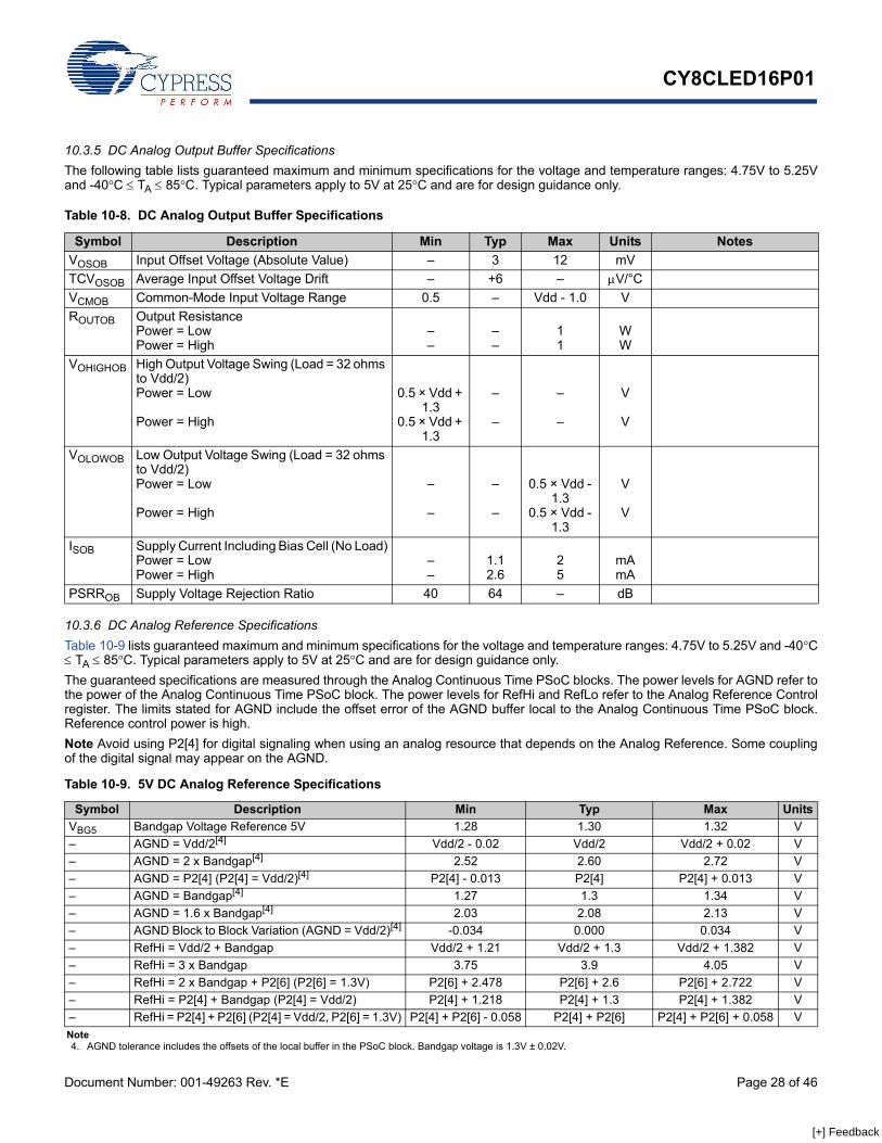
CY8CLED16P01
Document Number: 001-49263 Rev. *E Page 28 of 46
10.3.5 DC Analog Output Buffer SpecificationsThe following table lists guaranteed maximum and minimum specifications for the voltage and temperature ranges: 4.75V to 5.25Vand -40°C ≤ TA ≤ 85°C. Typical parameters apply to 5V at 25°C and are for design guidance only.
10.3.6 DC Analog Reference SpecificationsTable 10-9 lists guaranteed maximum and minimum specifications for the voltage and temperature ranges: 4.75V to 5.25V and -40°C≤ TA ≤ 85°C. Typical parameters apply to 5V at 25°C and are for design guidance only.The guaranteed specifications are measured through the Analog Continuous Time PSoC blocks. The power levels for AGND refer tothe power of the Analog Continuous Time PSoC block. The power levels for RefHi and RefLo refer to the Analog Reference Controlregister. The limits stated for AGND include the offset error of the AGND buffer local to the Analog Continuous Time PSoC block.Reference control power is high.Note Avoid using P2[4] for digital signaling when using an analog resource that depends on the Analog Reference. Some couplingof the digital signal may appear on the AGND.
Table 10-8. DC Analog Output Buffer Specifications
Symbol Description Min Typ Max Units NotesVOSOB Input Offset Voltage (Absolute Value) – 3 12 mVTCVOSOB Average Input Offset Voltage Drift – +6 – μV/°CVCMOB Common-Mode Input Voltage Range 0.5 – Vdd - 1.0 VROUTOB Output Resistance
Power = LowPower = High
––
––
11
WW
VOHIGHOB High Output Voltage Swing (Load = 32 ohms to Vdd/2)Power = Low
Power = High
0.5 × Vdd + 1.3
0.5 × Vdd + 1.3
–
–
–
–
V
V
VOLOWOB Low Output Voltage Swing (Load = 32 ohms to Vdd/2)Power = Low
Power = High
–
–
–
–
0.5 × Vdd - 1.3
0.5 × Vdd - 1.3
V
V
ISOB Supply Current Including Bias Cell (No Load)Power = LowPower = High
––
1.12.6
25
mAmA
PSRROB Supply Voltage Rejection Ratio 40 64 – dB
Table 10-9. 5V DC Analog Reference Specifications
Symbol Description Min Typ Max UnitsVBG5 Bandgap Voltage Reference 5V 1.28 1.30 1.32 V– AGND = Vdd/2[4] Vdd/2 - 0.02 Vdd/2 Vdd/2 + 0.02 V– AGND = 2 x Bandgap[4] 2.52 2.60 2.72 V– AGND = P2[4] (P2[4] = Vdd/2)[4] P2[4] - 0.013 P2[4] P2[4] + 0.013 V– AGND = Bandgap[4] 1.27 1.3 1.34 V– AGND = 1.6 x Bandgap[4] 2.03 2.08 2.13 V– AGND Block to Block Variation (AGND = Vdd/2)[4] -0.034 0.000 0.034 V– RefHi = Vdd/2 + Bandgap Vdd/2 + 1.21 Vdd/2 + 1.3 Vdd/2 + 1.382 V– RefHi = 3 x Bandgap 3.75 3.9 4.05 V– RefHi = 2 x Bandgap + P2[6] (P2[6] = 1.3V) P2[6] + 2.478 P2[6] + 2.6 P2[6] + 2.722 V– RefHi = P2[4] + Bandgap (P2[4] = Vdd/2) P2[4] + 1.218 P2[4] + 1.3 P2[4] + 1.382 V– RefHi = P2[4] + P2[6] (P2[4] = Vdd/2, P2[6] = 1.3V) P2[4] + P2[6] - 0.058 P2[4] + P2[6] P2[4] + P2[6] + 0.058 VNote4. AGND tolerance includes the offsets of the local buffer in the PSoC block. Bandgap voltage is 1.3V ± 0.02V.
[+] Feedback
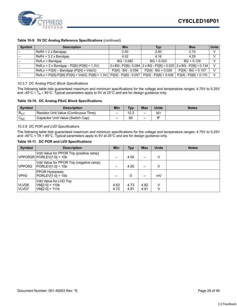
CY8CLED16P01
Document Number: 001-49263 Rev. *E Page 29 of 46
10.3.7 DC Analog PSoC Block SpecificationsThe following table lists guaranteed maximum and minimum specifications for the voltage and temperature ranges: 4.75V to 5.25Vand -40°C ≤ TA ≤ 85°C. Typical parameters apply to 5V at 25°C and are for design guidance only.
10.3.8 DC POR and LVD SpecificationsThe following table lists guaranteed maximum and minimum specifications for the voltage and temperature ranges: 4.75V to 5.25Vand -40°C = TA = 85°C. Typical parameters apply to 5V at 25°C and are for design guidance only.
– RefHi = 2 x Bandgap 2.50 2.60 2.70 V– RefHi = 3.2 x Bandgap 4.02 4.16 4.29 V– RefLo = Bandgap BG - 0.082 BG + 0.023 BG + 0.129 V– RefLo = 2 x Bandgap - P2[6] (P2[6] = 1.3V) 2 x BG - P2[6] - 0.084 2 x BG - P2[6] + 0.025 2 x BG - P2[6] + 0.134 V– RefLo = P2[4] – Bandgap (P2[4] = Vdd/2) P2[4] - BG - 0.056 P2[4] - BG + 0.026 P2[4] - BG + 0.107 V– RefLo = P2[4]-P2[6] (P2[4] = Vdd/2, P2[6] = 1.3V) P2[4] - P2[6] - 0.057 P2[4] - P2[6] + 0.026 P2[4] - P2[6] + 0.110 V
Table 10-9. 5V DC Analog Reference Specifications (continued)
Symbol Description Min Typ Max Units
Table 10-10. DC Analog PSoC Block Specifications
Symbol Description Min Typ Max Units NotesRCT Resistor Unit Value (Continuous Time) – 12.2 – kΩCSC Capacitor Unit Value (Switch Cap) – 80 – fF
Table 10-11. DC POR and LVD Specifications
Symbol Description Min Typ Max Units Notes
VPPOR2RVdd Value for PPOR Trip (positive ramp)PORLEV[1:0] = 10b – 4.55 – V
VPPOR2Vdd Value for PPOR Trip (negative ramp)PORLEV[1:0] = 10b – 4.55 – V
VPH2PPOR HysteresisPORLEV[1:0] = 10b – 0 – mV
VLVD6VLVD7
Vdd Value for LVD TripVM[2:0] = 110bVM[2:0] = 111b
4.634.72
4.734.81
4.824.91
VV
[+] Feedback
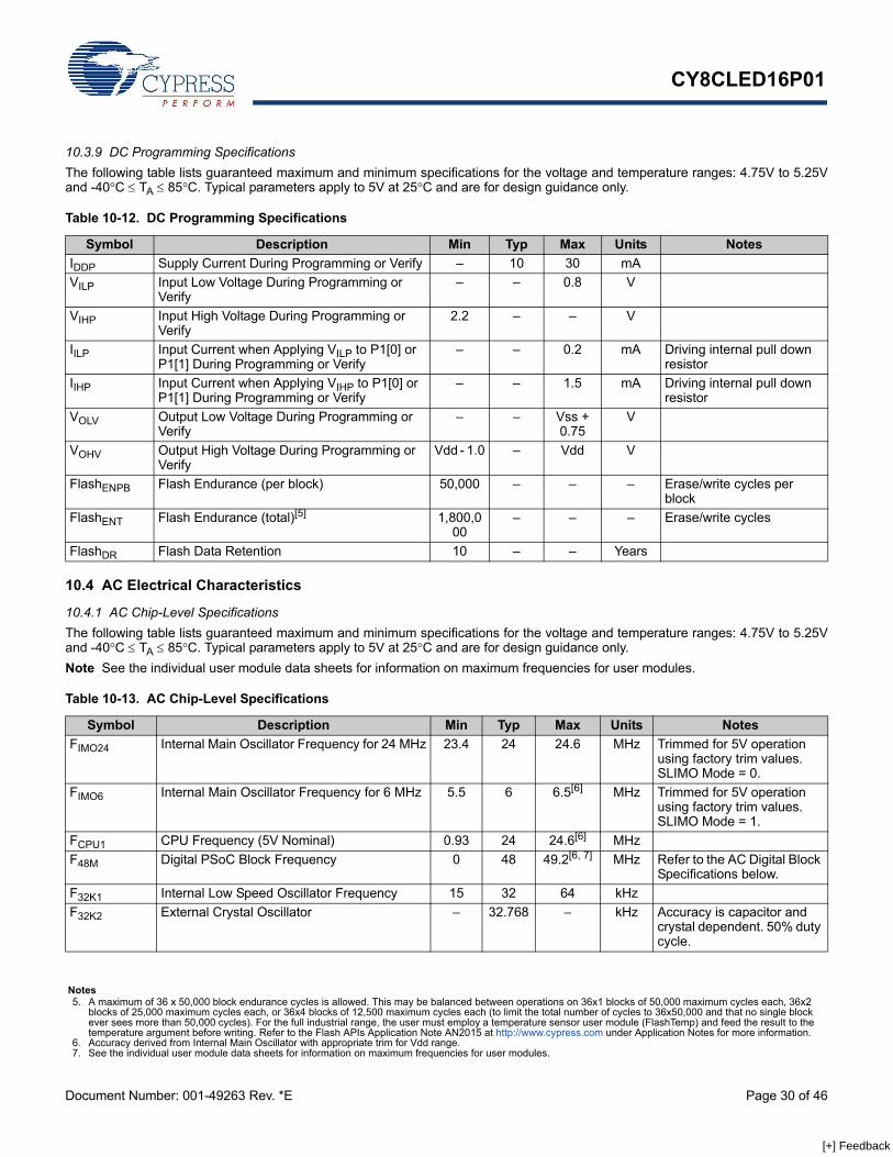
CY8CLED16P01
Document Number: 001-49263 Rev. *E Page 30 of 46
10.3.9 DC Programming SpecificationsThe following table lists guaranteed maximum and minimum specifications for the voltage and temperature ranges: 4.75V to 5.25Vand -40°C ≤ TA ≤ 85°C. Typical parameters apply to 5V at 25°C and are for design guidance only.
10.4 AC Electrical Characteristics
10.4.1 AC Chip-Level SpecificationsThe following table lists guaranteed maximum and minimum specifications for the voltage and temperature ranges: 4.75V to 5.25Vand -40°C ≤ TA ≤ 85°C. Typical parameters apply to 5V at 25°C and are for design guidance only.Note See the individual user module data sheets for information on maximum frequencies for user modules.
Table 10-12. DC Programming Specifications
Symbol Description Min Typ Max Units NotesIDDP Supply Current During Programming or Verify – 10 30 mAVILP Input Low Voltage During Programming or
Verify– – 0.8 V
VIHP Input High Voltage During Programming or Verify
2.2 – – V
IILP Input Current when Applying VILP to P1[0] or P1[1] During Programming or Verify
– – 0.2 mA Driving internal pull down resistor
IIHP Input Current when Applying VIHP to P1[0] or P1[1] During Programming or Verify
– – 1.5 mA Driving internal pull down resistor
VOLV Output Low Voltage During Programming or Verify
– – Vss + 0.75
V
VOHV Output High Voltage During Programming or Verify
Vdd - 1.0 – Vdd V
FlashENPB Flash Endurance (per block) 50,000 – – – Erase/write cycles per block
FlashENT Flash Endurance (total)[5] 1,800,000
– – – Erase/write cycles
FlashDR Flash Data Retention 10 – – Years
Table 10-13. AC Chip-Level Specifications
Symbol Description Min Typ Max Units NotesFIMO24 Internal Main Oscillator Frequency for 24 MHz 23.4 24 24.6 MHz Trimmed for 5V operation
using factory trim values. SLIMO Mode = 0.
FIMO6 Internal Main Oscillator Frequency for 6 MHz 5.5 6 6.5[6] MHz Trimmed for 5V operation using factory trim values. SLIMO Mode = 1.
FCPU1 CPU Frequency (5V Nominal) 0.93 24 24.6[6] MHzF48M Digital PSoC Block Frequency 0 48 49.2[6, 7] MHz Refer to the AC Digital Block
Specifications below.F32K1 Internal Low Speed Oscillator Frequency 15 32 64 kHzF32K2 External Crystal Oscillator – 32.768 – kHz Accuracy is capacitor and
crystal dependent. 50% duty cycle.
Notes5. A maximum of 36 x 50,000 block endurance cycles is allowed. This may be balanced between operations on 36x1 blocks of 50,000 maximum cycles each, 36x2
blocks of 25,000 maximum cycles each, or 36x4 blocks of 12,500 maximum cycles each (to limit the total number of cycles to 36x50,000 and that no single block ever sees more than 50,000 cycles). For the full industrial range, the user must employ a temperature sensor user module (FlashTemp) and feed the result to the temperature argument before writing. Refer to the Flash APIs Application Note AN2015 at http://www.cypress.com under Application Notes for more information.
6. Accuracy derived from Internal Main Oscillator with appropriate trim for Vdd range.7. See the individual user module data sheets for information on maximum frequencies for user modules.
[+] Feedback
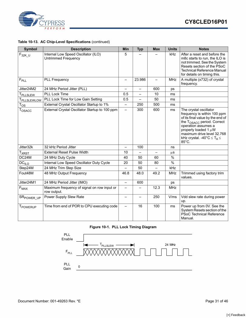
CY8CLED16P01
Document Number: 001-49263 Rev. *E Page 31 of 46
Figure 10-1. PLL Lock Timing Diagram
F32K_U Internal Low Speed Oscillator (ILO) Untrimmed Frequency
5 – – kHz After a reset and before the m8c starts to run, the ILO is not trimmed. See the System Resets section of the PSoC Technical Reference Manual for details on timing this.
FPLL PLL Frequency – 23.986 – MHz A multiple (x732) of crystal frequency.
Jitter24M2 24 MHz Period Jitter (PLL) – – 600 psTPLLSLEW PLL Lock Time 0.5 – 10 msTPLLSLEWLOW PLL Lock Time for Low Gain Setting 0.5 – 50 msTOS External Crystal Oscillator Startup to 1% – 250 500 msTOSACC External Crystal Oscillator Startup to 100 ppm – 300 600 ms The crystal oscillator
frequency is within 100 ppm of its final value by the end of the TOSACC period. Correct operation assumes a properly loaded 1 μW maximum drive level 32.768 kHz crystal. -40°C ≤ TA ≤ 85°C.
Jitter32k 32 kHz Period Jitter – 100 nsTXRST External Reset Pulse Width 10 – – μsDC24M 24 MHz Duty Cycle 40 50 60 %DCILO Internal Low Speed Oscillator Duty Cycle 20 50 80 %Step24M 24 MHz Trim Step Size – 50 – kHzFout48M 48 MHz Output Frequency 46.8 48.0 49.2 MHz Trimmed using factory trim
values.Jitter24M1 24 MHz Period Jitter (IMO) – 600 psFMAX Maximum frequency of signal on row input or
row output.– – 12.3 MHz
SRPOWER_UP Power Supply Slew Rate – – 250 V/ms Vdd slew rate during power up.
TPOWERUP Time from end of POR to CPU executing code – 16 100 ms Power up from 0V. See the System Resets section of the PSoC Technical Reference Manual.
Table 10-13. AC Chip-Level Specifications (continued)
Symbol Description Min Typ Max Units Notes
24 MHz
FPLL
PLLEnable
TPLLSLEW
PLLGain 0
[+] Feedback
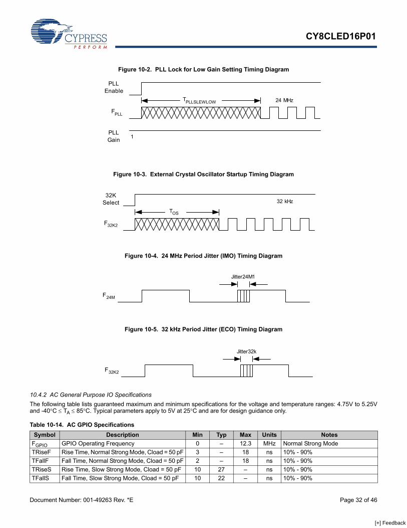
CY8CLED16P01
Document Number: 001-49263 Rev. *E Page 32 of 46
Figure 10-2. PLL Lock for Low Gain Setting Timing Diagram
Figure 10-3. External Crystal Oscillator Startup Timing Diagram
Figure 10-4. 24 MHz Period Jitter (IMO) Timing Diagram
Figure 10-5. 32 kHz Period Jitter (ECO) Timing Diagram
10.4.2 AC General Purpose IO SpecificationsThe following table lists guaranteed maximum and minimum specifications for the voltage and temperature ranges: 4.75V to 5.25Vand -40°C ≤ TA ≤ 85°C. Typical parameters apply to 5V at 25°C and are for design guidance only.
24 MHz
FPLL
PLLEnable
TPLLSLEWLOW
PLLGain 1
32 kHz
F32K2
32KSelect
TOS
Jitter24M1
F24M
Jitter32k
F32K2
Table 10-14. AC GPIO SpecificationsSymbol Description Min Typ Max Units Notes
FGPIO GPIO Operating Frequency 0 – 12.3 MHz Normal Strong ModeTRiseF Rise Time, Normal Strong Mode, Cload = 50 pF 3 – 18 ns 10% - 90%TFallF Fall Time, Normal Strong Mode, Cload = 50 pF 2 – 18 ns 10% - 90%TRiseS Rise Time, Slow Strong Mode, Cload = 50 pF 10 27 – ns 10% - 90%TFallS Fall Time, Slow Strong Mode, Cload = 50 pF 10 22 – ns 10% - 90%
[+] Feedback
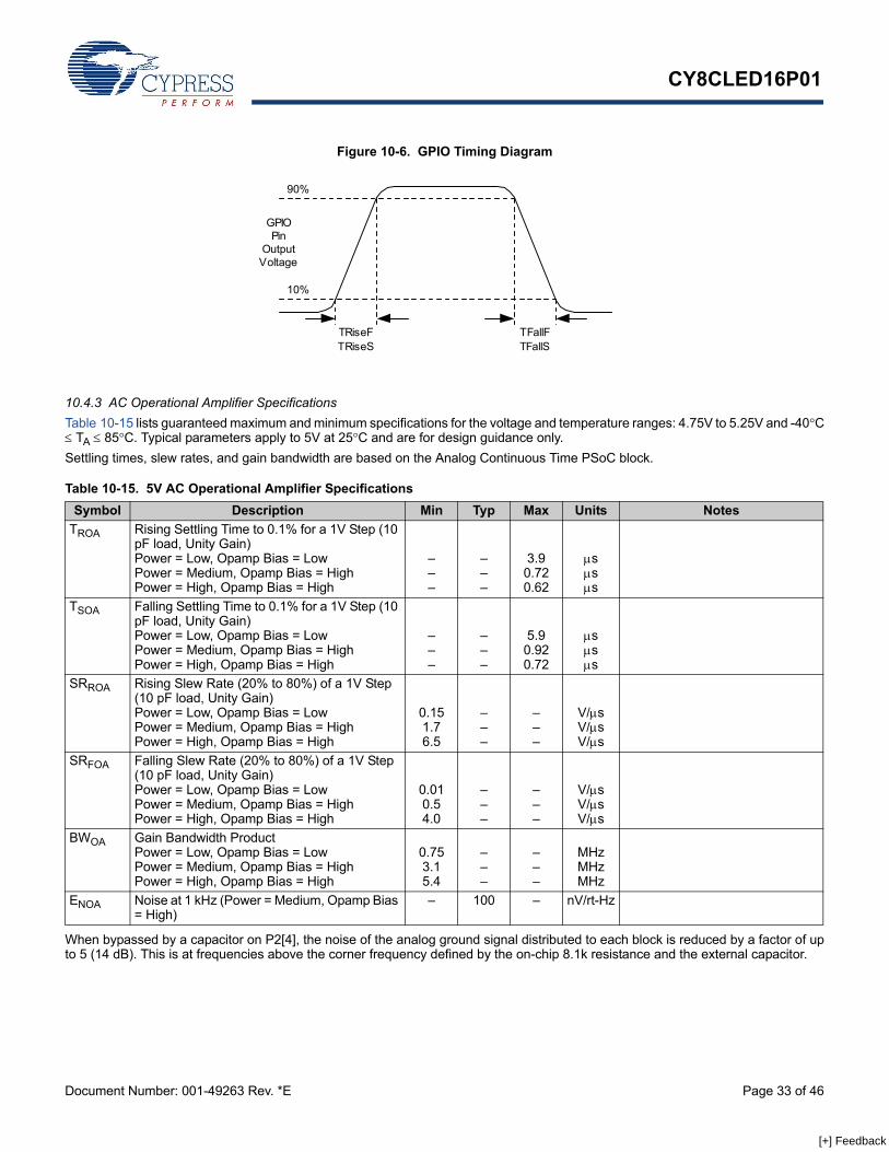
CY8CLED16P01
Document Number: 001-49263 Rev. *E Page 33 of 46
Figure 10-6. GPIO Timing Diagram
10.4.3 AC Operational Amplifier SpecificationsTable 10-15 lists guaranteed maximum and minimum specifications for the voltage and temperature ranges: 4.75V to 5.25V and -40°C≤ TA ≤ 85°C. Typical parameters apply to 5V at 25°C and are for design guidance only.Settling times, slew rates, and gain bandwidth are based on the Analog Continuous Time PSoC block.
When bypassed by a capacitor on P2[4], the noise of the analog ground signal distributed to each block is reduced by a factor of upto 5 (14 dB). This is at frequencies above the corner frequency defined by the on-chip 8.1k resistance and the external capacitor.
TFallFTFallS
TRiseFTRiseS
90%
10%
GPIOPin
OutputVoltage
Table 10-15. 5V AC Operational Amplifier SpecificationsSymbol Description Min Typ Max Units Notes
TROA Rising Settling Time to 0.1% for a 1V Step (10 pF load, Unity Gain)Power = Low, Opamp Bias = LowPower = Medium, Opamp Bias = HighPower = High, Opamp Bias = High
–––
–––
3.90.720.62
μsμsμs
TSOA Falling Settling Time to 0.1% for a 1V Step (10 pF load, Unity Gain)Power = Low, Opamp Bias = LowPower = Medium, Opamp Bias = HighPower = High, Opamp Bias = High
–––
–––
5.90.920.72
μsμsμs
SRROA Rising Slew Rate (20% to 80%) of a 1V Step (10 pF load, Unity Gain)Power = Low, Opamp Bias = LowPower = Medium, Opamp Bias = HighPower = High, Opamp Bias = High
0.151.76.5
–––
–––
V/μsV/μsV/μs
SRFOA Falling Slew Rate (20% to 80%) of a 1V Step (10 pF load, Unity Gain)Power = Low, Opamp Bias = LowPower = Medium, Opamp Bias = HighPower = High, Opamp Bias = High
0.010.54.0
–––
–––
V/μsV/μsV/μs
BWOA Gain Bandwidth Product Power = Low, Opamp Bias = LowPower = Medium, Opamp Bias = HighPower = High, Opamp Bias = High
0.753.15.4
–––
–––
MHzMHzMHz
ENOA Noise at 1 kHz (Power = Medium, Opamp Bias = High)
– 100 – nV/rt-Hz
[+] Feedback
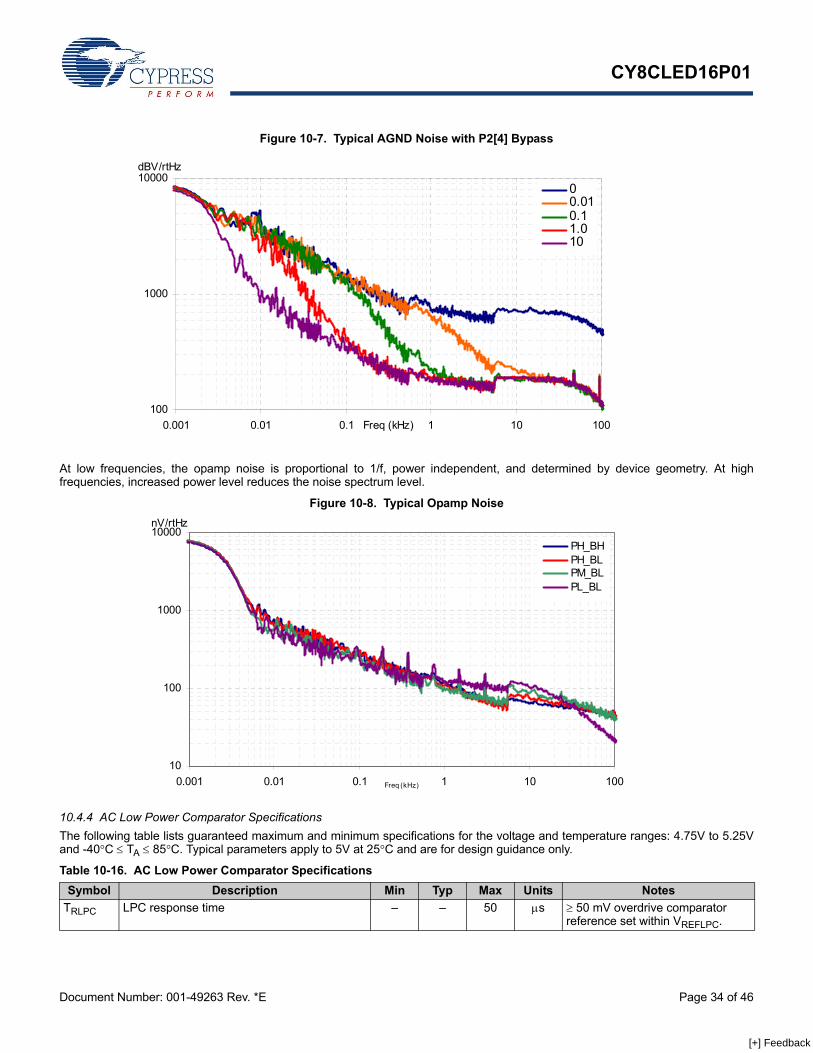
CY8CLED16P01
Document Number: 001-49263 Rev. *E Page 34 of 46
Figure 10-7. Typical AGND Noise with P2[4] Bypass
At low frequencies, the opamp noise is proportional to 1/f, power independent, and determined by device geometry. At highfrequencies, increased power level reduces the noise spectrum level.
Figure 10-8. Typical Opamp Noise
10.4.4 AC Low Power Comparator SpecificationsThe following table lists guaranteed maximum and minimum specifications for the voltage and temperature ranges: 4.75V to 5.25Vand -40°C ≤ TA ≤ 85°C. Typical parameters apply to 5V at 25°C and are for design guidance only.
100
1000
10000
0.001 0.01 0.1 1 10 100Freq (kHz)
dBV/rtHz
00.010.11.010
10
100
1000
10000
0.001 0.01 0.1 1 10 100Freq (kHz)
nV/rtHz
PH_BHPH_BLPM_BLPL_BL
Table 10-16. AC Low Power Comparator SpecificationsSymbol Description Min Typ Max Units Notes
TRLPC LPC response time – – 50 μs ≥ 50 mV overdrive comparator reference set within VREFLPC.
[+] Feedback
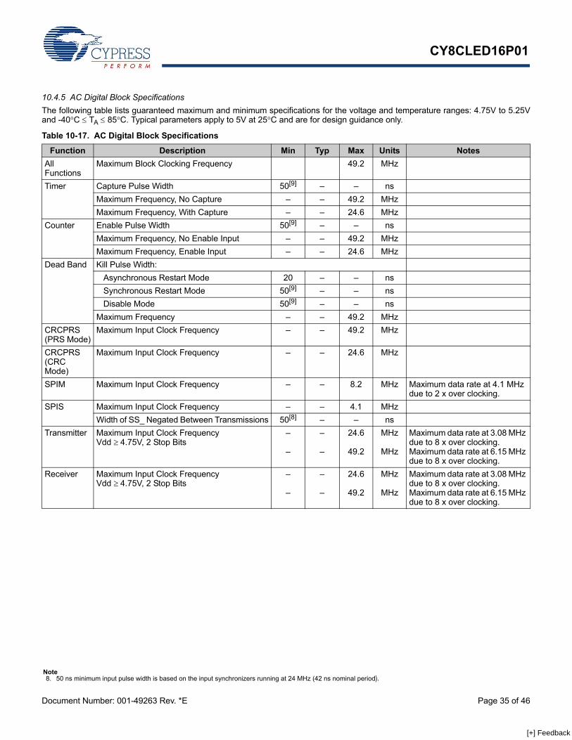
CY8CLED16P01
Document Number: 001-49263 Rev. *E Page 35 of 46
10.4.5 AC Digital Block SpecificationsThe following table lists guaranteed maximum and minimum specifications for the voltage and temperature ranges: 4.75V to 5.25Vand -40°C ≤ TA ≤ 85°C. Typical parameters apply to 5V at 25°C and are for design guidance only.
Table 10-17. AC Digital Block Specifications
Function Description Min Typ Max Units NotesAll Functions
Maximum Block Clocking Frequency 49.2 MHz
Timer Capture Pulse Width 50[9] – – nsMaximum Frequency, No Capture – – 49.2 MHzMaximum Frequency, With Capture – – 24.6 MHz
Counter Enable Pulse Width 50[9] – – nsMaximum Frequency, No Enable Input – – 49.2 MHzMaximum Frequency, Enable Input – – 24.6 MHz
Dead Band Kill Pulse Width:Asynchronous Restart Mode 20 – – nsSynchronous Restart Mode 50[9] – – nsDisable Mode 50[9] – – ns
Maximum Frequency – – 49.2 MHzCRCPRS(PRS Mode)
Maximum Input Clock Frequency – – 49.2 MHz
CRCPRS(CRC Mode)
Maximum Input Clock Frequency – – 24.6 MHz
SPIM Maximum Input Clock Frequency – – 8.2 MHz Maximum data rate at 4.1 MHz due to 2 x over clocking.
SPIS Maximum Input Clock Frequency – – 4.1 MHzWidth of SS_ Negated Between Transmissions 50[8] – – ns
Transmitter Maximum Input Clock FrequencyVdd ≥ 4.75V, 2 Stop Bits
–
–
–
–
24.6
49.2
MHz
MHz
Maximum data rate at 3.08 MHz due to 8 x over clocking.Maximum data rate at 6.15 MHz due to 8 x over clocking.
Receiver Maximum Input Clock FrequencyVdd ≥ 4.75V, 2 Stop Bits
–
–
–
–
24.6
49.2
MHz
MHz
Maximum data rate at 3.08 MHz due to 8 x over clocking.Maximum data rate at 6.15 MHz due to 8 x over clocking.
Note8. 50 ns minimum input pulse width is based on the input synchronizers running at 24 MHz (42 ns nominal period).
[+] Feedback
CY8CLED16P01
Document Number: 001-49263 Rev. *E Page 36 of 46
10.4.6 AC Analog Output Buffer SpecificationsThe following table lists guaranteed maximum and minimum specifications for the voltage and temperature ranges: 4.75V to 5.25Vand -40°C ≤ TA ≤ 85°C. Typical parameters apply to 5V at 25°C and are for design guidance only.
10.4.7 AC External Clock SpecificationsThe following tables list guaranteed maximum and minimum specifications for the voltage and temperature ranges: 4.75V to 5.25Vand -40°C ≤ TA ≤ 85°C. Typical parameters apply to 5V at 25°C and are for design guidance only.
10.4.8 AC Programming SpecificationsThe following table lists guaranteed maximum and minimum specifications for the voltage and temperature ranges: 4.75V to 5.25Vand -40°C ≤ TA ≤ 85°C. Typical parameters apply to 5V at 25°C and are for design guidance only.
Table 10-18. 5V AC Analog Output Buffer Specifications
Symbol Description Min Typ Max Units NotesTROB Rising Settling Time to 0.1%, 1V Step, 100 pF
LoadPower = LowPower = High
––
––
44
μsμs
TSOB Falling Settling Time to 0.1%, 1V Step, 100 pF LoadPower = Low Power = High
––
––
3.43.4
μsμs
SRROB Rising Slew Rate (20% to 80%), 1V Step, 100 pF LoadPower = LowPower = High
0.50.5
––
––
V/μsV/μs
SRFOB Falling Slew Rate (80% to 20%), 1V Step, 100 pF LoadPower = LowPower = High
0.550.55
––
––
V/μsV/μs
BWOB Small Signal Bandwidth, 20mVpp, 3 dB BW, 100 pF LoadPower = LowPower = High
0.80.8
––
––
MHzMHz
BWOB Large Signal Bandwidth, 1Vpp, 3 dB BW, 100 pF LoadPower = LowPower = High
300300
––
––
kHzkHz
Table 10-19. 5V AC External Clock Specifications
Symbol Description Min Typ Max Units NotesFOSCEXT Frequency 0.093 – 24.6 MHz– High Period 20.6 – 5300 ns– Low Period 20.6 – – ns– Power Up IMO to Switch 150 – – µs
Table 10-20. AC Programming Specifications
Symbol Description Min Typ Max Units NotesTRSCLK Rise Time of SCLK 1 – 20 nsTFSCLK Fall Time of SCLK 1 – 20 nsTSSCLK Data Setup Time to Falling Edge of SCLK 40 – – nsTHSCLK Data Hold Time from Falling Edge of SCLK 40 – – nsFSCLK Frequency of SCLK 0 – 8 MHzTERASEB Flash Erase Time (Block) – 10 – msTWRITE Flash Block Write Time – 40 – ms
[+] Feedback
CY8CLED16P01
Document Number: 001-49263 Rev. *E Page 37 of 46
10.4.9 AC I2C SpecificationsThe following table lists guaranteed maximum and minimum specifications for the voltage and temperature ranges: 4.75V to 5.25Vand -40°C ≤ TA ≤ 85°C. Typical parameters apply to 5V at 25°C and are for design guidance only.
Figure 10-9. Definition for Timing for Fast/Standard Mode on the I2C Bus Packaging Dimensions
TDSCLK Data Out Delay from Falling Edge of SCLK – – 45 nsTERASEALL Flash Erase Time (Bulk) – 80 – ms Erase all Blocks and protection
fields at onceTPROGRAM_HOT Flash Block Erase + Flash Block Write Time – – 100[9] ms 0°C <= Tj <= 100°CTPROGRAM_COLD Flash Block Erase + Flash Block Write Time – – 200[9] ms -40°C <= Tj <= 0°C
Table 10-21. AC Characteristics of the I2C SDA and SCL Pins
Symbol DescriptionStandard Mode Fast Mode
Units NotesMin Max Min Max
FSCLI2C SCL Clock Frequency 0 100 0 400 kHzTHDSTAI2C Hold Time (repeated) START Condition. After
this period, the first clock pulse is generated.4.0 – 0.6 – μs
TLOWI2C LOW Period of the SCL Clock 4.7 – 1.3 – μsTHIGHI2C HIGH Period of the SCL Clock 4.0 – 0.6 – μsTSUSTAI2C Setup Time for a Repeated START Condition 4.7 – 0.6 – μsTHDDATI2C Data Hold Time 0 – 0 – μsTSUDATI2C Data Setup Time 250 – 100[10] – nsTSUSTOI2C Setup Time for STOP Condition 4.0 – 0.6 – μsTBUFI2C Bus Free Time Between a STOP and START
Condition4.7 – 1.3 – μs
TSPI2C Pulse Width of spikes are suppressed by the input filter
– – 0 50 ns
Table 10-20. AC Programming Specifications (continued)
Symbol Description Min Typ Max Units Notes
Notes9. For the full industrial range, the user must employ a temperature sensor user module (FlashTemp) and feed the result to the temperature argument before writing.
Refer to the Flash APIs Application Note AN2015 at http://www.cypress.com for more information.10. A Fast-Mode I2C-bus device can be used in a Standard-Mode I2C-bus system, but the requirement tSU;DAT ≥ 250 ns must then be met. This is automatically the case
if the device does not stretch the LOW period of the SCL signal. If this device does stretch the LOW period of the SCL signal, it must output the next data bit to the SDA line trmax + tSU;DAT = 1000 + 250 = 1250 ns (according to the Standard-Mode I2C-bus specification) before the SCL line is released.
SDA
SCL
S Sr SP
TBUFI2C
TSPI2CTHDSTAI2C
TSUSTOI2CTSUSTAI2C
TLOWI2C
THIGHI2CTHDDATI2CTHDSTAI2C
TSUDATI2C
[+] Feedback
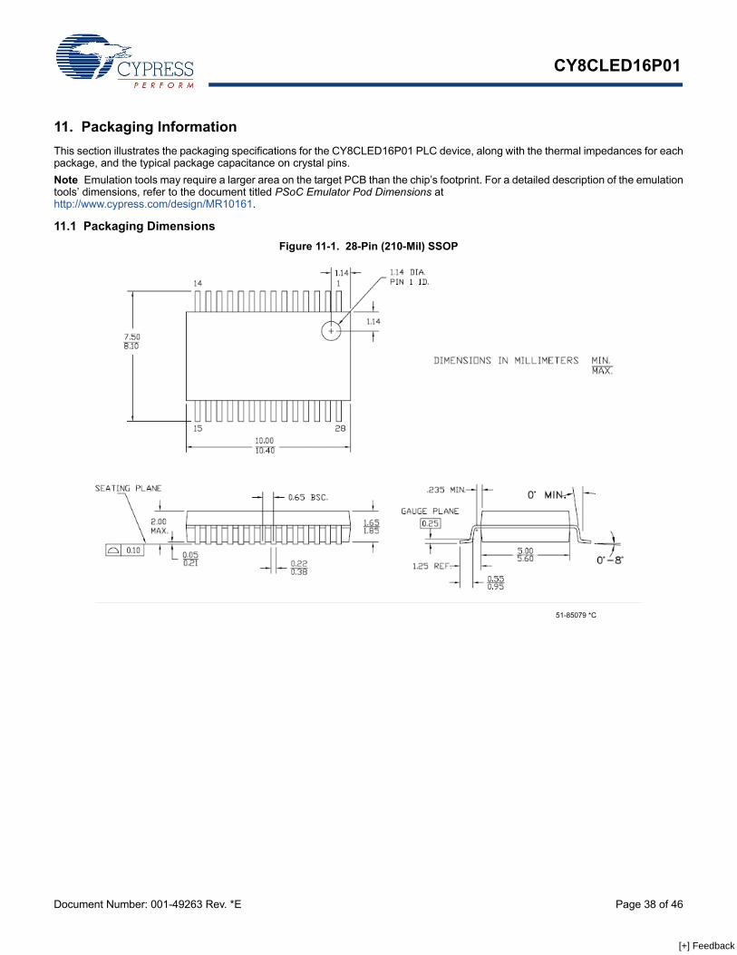
CY8CLED16P01
Document Number: 001-49263 Rev. *E Page 38 of 46
11. Packaging InformationThis section illustrates the packaging specifications for the CY8CLED16P01 PLC device, along with the thermal impedances for eachpackage, and the typical package capacitance on crystal pins.Note Emulation tools may require a larger area on the target PCB than the chip’s footprint. For a detailed description of the emulationtools’ dimensions, refer to the document titled PSoC Emulator Pod Dimensions at http://www.cypress.com/design/MR10161.
11.1 Packaging DimensionsFigure 11-1. 28-Pin (210-Mil) SSOP
51-85079 *C
[+] Feedback
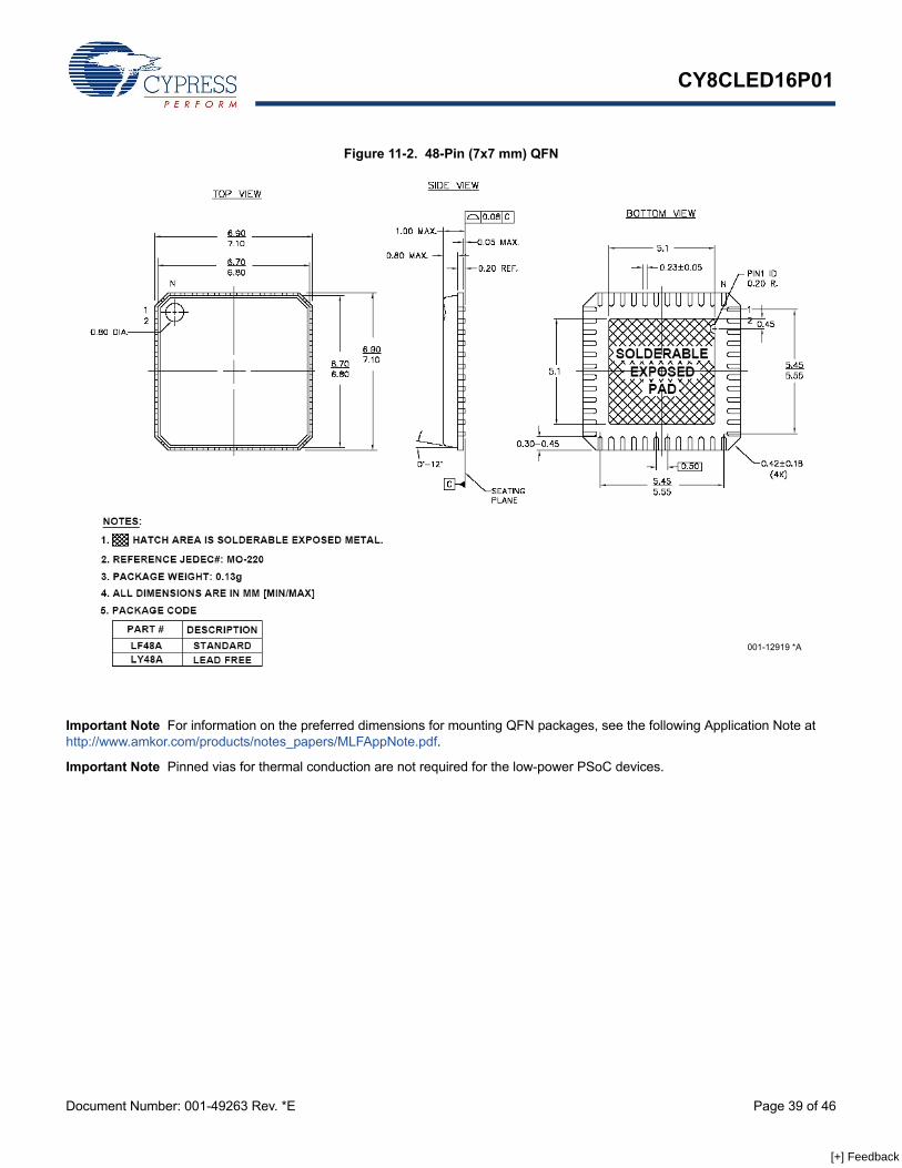
CY8CLED16P01
Document Number: 001-49263 Rev. *E Page 39 of 46
Figure 11-2. 48-Pin (7x7 mm) QFN
Important Note For information on the preferred dimensions for mounting QFN packages, see the following Application Note athttp://www.amkor.com/products/notes_papers/MLFAppNote.pdf.
Important Note Pinned vias for thermal conduction are not required for the low-power PSoC devices.
001-12919 *A
[+] Feedback
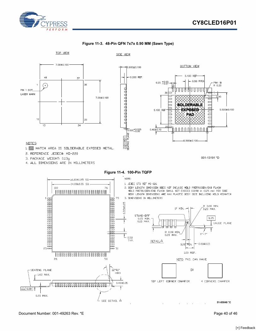
CY8CLED16P01
Document Number: 001-49263 Rev. *E Page 40 of 46
Figure 11-3. 48-Pin QFN 7x7x 0.90 MM (Sawn Type)
Figure 11-4. 100-Pin TQFP
001-13191 *D
51-85048 **51-85048 **
51-85048 *C
[+] Feedback
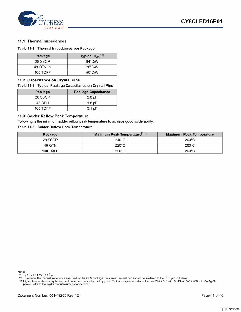
CY8CLED16P01
Document Number: 001-49263 Rev. *E Page 41 of 46
11.1 Thermal Impedances
11.2 Capacitance on Crystal Pins
11.3 Solder Reflow Peak TemperatureFollowing is the minimum solder reflow peak temperature to achieve good solderability.
Table 11-1. Thermal Impedances per Package
Package Typical θJA[11]
28 SSOP 94°C/W48 QFN[12] 28°C/W100 TQFP 50°C/W
Table 11-2. Typical Package Capacitance on Crystal Pins
Package Package Capacitance28 SSOP 2.8 pF48 QFN 1.8 pF
100 TQFP 3.1 pF
Table 11-3. Solder Reflow Peak Temperature
Package Minimum Peak Temperature[13] Maximum Peak Temperature28 SSOP 240°C 260°C48 QFN 220°C 260°C
100 TQFP 220°C 260°C
Notes11. TJ = TA + POWER × θJA 12. To achieve the thermal impedance specified for the QFN package, the center thermal pad should be soldered to the PCB ground plane.13. Higher temperatures may be required based on the solder melting point. Typical temperatures for solder are 220 ± 5°C with Sn-Pb or 245 ± 5°C with Sn-Ag-Cu
paste. Refer to the solder manufacturer specifications.
[+] Feedback

CY8CLED16P01
Document Number: 001-49263 Rev. *E Page 42 of 46
12. Development Tool Selection12.1 Software12.1.1 PSoC Designer™At the core of the PSoC development software suite is PSoCDesigner. Utilized by thousands of PSoC developers, this robustsoftware has been facilitating PSoC designs for years. PSoCDesigner is available free of charge at http://www.cypress.com.PSoC Designer comes with a free C compiler.12.1.2 PSoC ProgrammerPSoC Programmer is a very flexible programming application. Itis used on the bench in development and is also suitable forfactory programming. PSoC Programmer works either in astandalone configuration or operates directly from PSoCDesigner. PSoC Programmer software is compatible with bothPSoC ICE Cube In-Circuit Emulator and PSoC MiniProg. PSoCprogrammer is available free of charge athttp://www.cypress.com/psocprogrammer.
12.2 Development KitsAll development kits are sold at the Cypress Online Store.
12.2.1 CY3276-Programmable HV PLC + EZ-Color™ Devel-opment Kit
The CY3276 is used for prototyping and development on theCY8CLED16P01 with PSoC Designer. This kit supports in-circuitemulation. The software interface enables users to run, halt, andsingle-step the processor and view the content of specificmemory locations. PSoC Designer also supports the advancedemulation features. The hardware contains the high voltagecoupling circuit for 110 VAC to 240 VAC powerline, which iscompliant with the CENELEC/FCC standards. This board alsohas an onboard switch mode power supply. The kit includes:■ One High Voltage (110 to 230VAC) PLC Board. Cypress recom-
mends that a user purchases two CY3276 kits to set up a two-node PLC subsystem for evaluation and development.
■ LED Daughter Card■ CY8CLED16P01-OCD (100 TQFP)■ Software CD■ Supporting Literature■ MiniProg1
12.2.2 CY3277-Programmable LV PLC + EZ-Color Development Kit
The CY3277-PLC is used for prototyping and development onthe CY8CLED16P01 with PSoC Designer. This kit supportsin-circuit emulation. The software interface enables users to run,halt, and single-step the processor and view the content ofspecific memory locations. PSoC Designer also supportsadvanced emulation features. The hardware contains the lowvoltage coupling circuit for 12-24V AC/DC powerline. The kitincludes:
■ One Low Voltage (12 to 24V AC/DC) PLC Board. Cypress recommends that a user purchases two CY3275 kits to set up a two-node PLC subsystem for evaluation and development
■ LED Daughter Card■ CY8CLED16P01-OCD (100 TQFP)■ Software CD■ Supporting Literature■ MiniProg1
12.2.3 CY3250-PLC Pod KitsThe CY3250-PLC Pod Kits are essential for developmentpurposes as they provide the users a medium to emulate anddebug their designs. The pod kits are available for all theavailable footprints. The details are:
■ CY3250-LED16P01NQ – One SSOP Pod (CY8CLED16P01-OCD), Two 28-SSOP Feet, One 3250-Flex Cable, One 28-SSOP Foot Mask
■ CY3250-LED16P01QFN – One QFN Pod (CY8CLED16P01-OCD), Two 48-QFN Feet, One 3250-Flex Cable
■ CY3250-LED16P01NQ-POD – Two SSOP Pods (CY8CLED16P01-OCD)
■ CY3250-LED16P01QFN-POD – Two QFN Pods (CY8CLED16P01-OCD)
12.2.4 CY3215-DK Basic Development KitThe CY3215-DK is used for prototyping and development withPSoC Designer. This kit can be used in conjunction with the PLCkits to support in-circuit emulation. The software interfaceenables users to run, halt, and single step the processor andview the content of specific memory locations. PSoC Designeralso supports the advanced emulation features. The kit includes:
■ PSoC Designer Software CD
■ ICE-Cube In-Circuit Emulator
■ ICE Flex-Pod for CY8C29x66 Family
■ Cat-5 Adapter
■ Mini-Eval Programming Board
■ 110 ~ 240V Power Supply, Euro-Plug Adapter
■ iMAGEcraft C Compiler (Registration Required)
■ ISSP Cable
■ USB 2.0 Cable and Blue Cat-5 Cable
■ 2 CY8C29466-24PXI 28-PDIP Chip Samples
[+] Feedback
CY8CLED16P01
Document Number: 001-49263 Rev. *E Page 43 of 46
12.3 Evaluation KitsThe evaluation kits do not have on-board powerline capability,but can be used with a PLC kit for evaluation purposes. All evalu-ation tools are sold at the Cypress Online Store.
12.3.1 CY3210-MiniProg1The CY3210-MiniProg1 kit enables the user to program PSoCdevices via the MiniProg1 programming unit. The MiniProg is asmall, compact prototyping programmer that connects to the PCvia a provided USB 2.0 cable. The kit includes:
■ MiniProg Programming Unit
■ MiniEval Socket Programming and Evaluation Board
■ 28-Pin CY8C29466-24PXI PDIP PSoC Device Sample
■ 28-Pin CY8C27443-24PXI PDIP PSoC Device Sample
■ PSoC Designer Software CD
■ Getting Started Guide
■ USB 2.0 Cable
12.3.2 CY3210-PSoCEval1The CY3210-PSoCEval1 kit features an evaluation board andthe MiniProg1 programming unit. The evaluation board includesan LCD module, potentiometer, LEDs, and plenty of breadboarding space to meet all of your evaluation needs. The kitincludes:
■ Evaluation Board with LCD Module
■ MiniProg Programming Unit
■ 28-Pin CY8C29466-24PXI PDIP PSoC Device Sample (2)
■ PSoC Designer Software CD
■ Getting Started Guide
■ USB 2.0 Cable
12.3.3 CY3214-PSoCEvalUSB The CY3214-PSoCEvalUSB evaluation kit features a devel-opment board for the CY8C24794-24LFXI PSoC device. Specialfeatures of the board include both USB and capacitive sensingdevelopment and debugging support. This evaluation board alsoincludes an LCD module, potentiometer, LEDs, an enunciator,and plenty of bread boarding space to meet all of your evaluationneeds. The kit includes:
■ PSoCEvalUSB Board
■ LCD Module
■ MIniProg Programming Unit
■ Mini USB Cable
■ PSoC Designer and Example Projects CD
■ Getting Started Guide
■ Wire Pack
12.4 Device ProgrammersAll device programmers are purchased from the Cypress OnlineStore.
12.4.1 CY3216 Modular ProgrammerThe CY3216 Modular Programmer kit features a modularprogrammer and the MiniProg1 programming unit. The modularprogrammer includes three programming module cards andsupports multiple Cypress products. The kit includes:
■ Modular Programmer Base
■ Three Programming Module Cards
■ MiniProg Programming Unit
■ PSoC Designer Software CD
■ Getting Started Guide
■ USB 2.0 Cable
12.4.2 CY3207 ISSP In-System Serial Programmer (ISSP)The CY3207ISSP is a production programmer. It includesprotection circuitry and an industrial case that is more robust thanthe MiniProg in a production programming environment.Note that CY3207ISSP needs special software and is notcompatible with PSoC Programmer. The kit includes:
■ CY3207 Programmer Unit
■ PSoC ISSP Software CD
■ 110 ~ 240V Power Supply, Euro-Plug Adapter
■ USB 2.0 Cable
12.4.3 Third Party ToolsSeveral tools are specially designed by the following third partyvendors to accompany PSoC devices during development andproduction. Specific details of each of these tools are found athttp://www.cypress.com under Support.
12.4.4 Build a PSoC Emulator into Your Board
For details on emulating the circuit before going to volume pro-duction using an on-chip debug (OCD) non-production PSoCdevice, see Application Note AN2323 Debugging - Build aPSoC Emulator into Your Board athttp://www.cypress.com/design/AN2323.
[+] Feedback
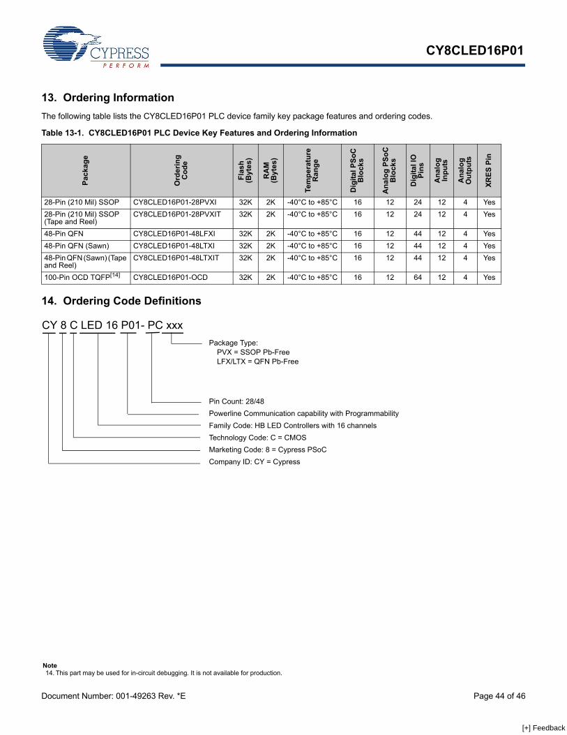
CY8CLED16P01
Document Number: 001-49263 Rev. *E Page 44 of 46
13. Ordering InformationThe following table lists the CY8CLED16P01 PLC device family key package features and ordering codes.
14. Ordering Code Definitions
Table 13-1. CY8CLED16P01 PLC Device Key Features and Ordering Information
Pack
age
Ord
erin
gC
ode
Flas
h(B
ytes
)
RA
M(B
ytes
)
Tem
pera
ture
Ran
ge
Dig
ital P
SoC
Blo
cks
Ana
log
PSoC
Blo
cks
Dig
ital I
OPi
ns
Ana
log
Inpu
ts
Ana
log
Out
puts
XRES
Pin
28-Pin (210 Mil) SSOP CY8CLED16P01-28PVXI 32K 2K -40°C to +85°C 16 12 24 12 4 Yes28-Pin (210 Mil) SSOP (Tape and Reel)
CY8CLED16P01-28PVXIT 32K 2K -40°C to +85°C 16 12 24 12 4 Yes
48-Pin QFN CY8CLED16P01-48LFXI 32K 2K -40°C to +85°C 16 12 44 12 4 Yes48-Pin QFN (Sawn) CY8CLED16P01-48LTXI 32K 2K -40°C to +85°C 16 12 44 12 4 Yes48-Pin QFN (Sawn) (Tape and Reel)
CY8CLED16P01-48LTXIT 32K 2K -40°C to +85°C 16 12 44 12 4 Yes
100-Pin OCD TQFP[14] CY8CLED16P01-OCD 32K 2K -40°C to +85°C 16 12 64 12 4 Yes
CY 8 C LED 16 P01- PC xxxPackage Type:
PVX = SSOP Pb-FreeLFX/LTX = QFN Pb-Free
Pin Count: 28/48Powerline Communication capability with ProgrammabilityFamily Code: HB LED Controllers with 16 channelsTechnology Code: C = CMOSMarketing Code: 8 = Cypress PSoCCompany ID: CY = Cypress
Note14. This part may be used for in-circuit debugging. It is not available for production.
[+] Feedback
CY8CLED16P01
Document Number: 001-49263 Rev. *E Page 45 of 46
15. Document History Page
Document Title: CY8CLED16P01 Powerline Communication SolutionDocument Number: 001-49263
Rev. ECN No. Orig. of Change
Submission Date Description of Change
** 2575716 GHH/PYRS 10/01/08 New Datasheet*A 2731927 GHH/HMT/
DSG07/06/09 Added
- Configurable baud rates and FSK Frequencies- PLC Pod Kits for development purposesModified- Pin information for all packages
*B 2748537 GHH See ECN Added Sections on ‘Getting Started’ and ‘Document Conventions’Modified the following Electrical Parameters- FIMO6 Min: Changed from 5.75 MHz to 5.5 MHz- FIMO6 Max: Changed from 6.35 MHz to 6.5 MHz- SPIS (Maximum input clock frequency): Changed from 4.1 ns to 4.1 MHz- TWRITE (Flash Block Write Time): Changed from 40 ms to 10 ms
*C 2752799 GHH 08/17/09 Posting to external web.*D 2759000 GHH 09/02/2009 Fixed typos in the data sheet.
Updated Figure 1-2. on page 2 and Figure 3-1. on page 10.*E 2778970 FRE 10/05/2009 Added a table for DC POR and LVD Specifications
Updated DC GPIO, AC Chip-Level, and AC Programming Specifications as follows:- Modified FIMO6, TWRITE, and Power Up IMO to Switch specifications- Added IOH, IOL, DCILO, F32K_U, TPOWERUP, TERASEALL, and SRPOWER_UP specificationsAdded 48-Pin QFN (Sawn) package diagram and CY8CLED16P01-48LTXI and CY8CLED16P01-48LTXIT part details in the Ordering Information tableUpdated section 5 and Tables 10-1, 10-2, and 10-3 to state the requirement to use the external crystal for PLC protocol timingTable 10-1 and Figure 10-1: Changed pins 9 and 25 from NC to RSVDTable 10-2 and Figure 10-2: Changed pins 7 and 39 from NC to RSVDTable 10-3 and Figure 10-3: Changed pins 14 and 77 from NC to RSVDTables 10-1, 10-2, 10-3: Added explanation to Connect a 0.1 uF capacitor between XTAL_Stability and VSS.Fixed minor typos
[+] Feedback
Document Number: 001-49263 Rev. *E Revised October 05, 2009 Page 46 of 46
PSoC® and CapSense® are registered trademarks and PSoC Designer and EZ-Color are trademarks of Cypress Semiconductor Corp. All products and company names mentioned in this documentmay be the trademarks of their respective holders.
CY8CLED16P01
© Cypress Semiconductor Corporation, 2008-2009. The information contained herein is subject to change without notice. Cypress Semiconductor Corporation assumes no responsibility for the use ofany circuitry other than circuitry embodied in a Cypress product. Nor does it convey or imply any license under patent or other rights. Cypress products are not warranted nor intended to be used formedical, life support, life saving, critical control or safety applications, unless pursuant to an express written agreement with Cypress. Furthermore, Cypress does not authorize its products for use ascritical components in life-support systems where a malfunction or failure may reasonably be expected to result in significant injury to the user. The inclusion of Cypress products in life-support systemsapplication implies that the manufacturer assumes all risk of such use and in doing so indemnifies Cypress against all charges.
Any Source Code (software and/or firmware) is owned by Cypress Semiconductor Corporation (Cypress) and is protected by and subject to worldwide patent protection (United States and foreign),United States copyright laws and international treaty provisions. Cypress hereby grants to licensee a personal, non-exclusive, non-transferable license to copy, use, modify, create derivative works of,and compile the Cypress Source Code and derivative works for the sole purpose of creating custom software and or firmware in support of licensee product to be used only in conjunction with a Cypressintegrated circuit as specified in the applicable agreement. Any reproduction, modification, translation, compilation, or representation of this Source Code except as specified above is prohibited withoutthe express written permission of Cypress.
Disclaimer: CYPRESS MAKES NO WARRANTY OF ANY KIND, EXPRESS OR IMPLIED, WITH REGARD TO THIS MATERIAL, INCLUDING, BUT NOT LIMITED TO, THE IMPLIED WARRANTIESOF MERCHANTABILITY AND FITNESS FOR A PARTICULAR PURPOSE. Cypress reserves the right to make changes without further notice to the materials described herein. Cypress does notassume any liability arising out of the application or use of any product or circuit described herein. Cypress does not authorize its products for use as critical components in life-support systems wherea malfunction or failure may reasonably be expected to result in significant injury to the user. The inclusion of Cypress’ product in a life-support systems application implies that the manufacturerassumes all risk of such use and in doing so indemnifies Cypress against all charges.
Use may be limited by and subject to the applicable Cypress software license agreement.
16. Sales, Solutions, and Legal InformationWorldwide Sales and Design SupportCypress maintains a worldwide network of offices, solution centers, manufacturer’s representatives, and distributors. To find the officeclosest to you, visit us at www.cypress.com/go/home/order/sales.
ProductsPSoC psoc.cypress.comClocks & Buffers clocks.cypress.comWireless wireless.cypress.comMemories memory.cypress.comImage Sensors image.cypress.com
[+] Feedback