Embed Size (px)
Citation preview
1dc1676af
DEMO MANUAL DC1676A
Description
LTC4359HDCB 28V/20A Ideal Diode and Switch with Reverse Input
Protection
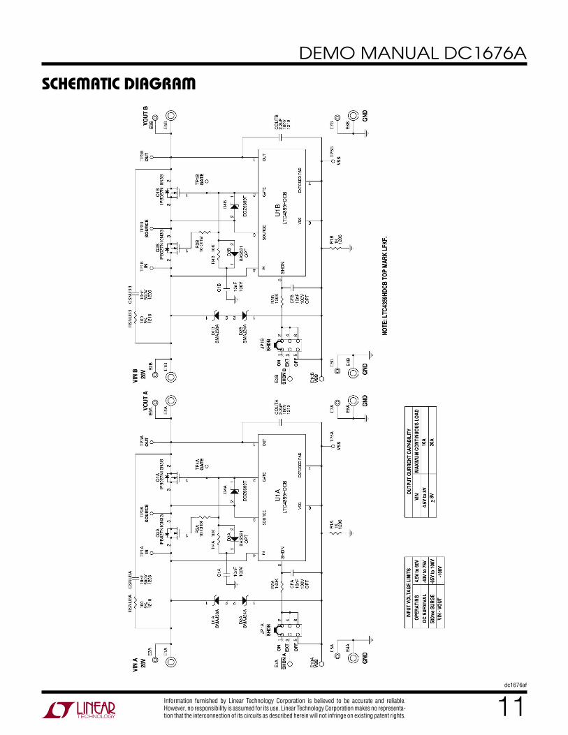
Demonstration Circuit 1676A showcases the LTC®4359 ideal diode controller with reverse input protection. The board includes two independent LTC4359 ideal diode circuits, sharing a common ground and operating over a 4.5V to 60V range. Each circuit comprises a load switch and ideal diode connected in series. Power to the load may be turned on and off by using the SHDN input, and the load is protected against reverse inputs of up to –40VDC by the ideal diode. In addition, input dropouts are blocked from the output, permitting capacitors or a battery to hold up the load when input power fails.
L, LT, LTC, LTM, Linear Technology and the Linear logo are registered trademarks of Linear Technology Corporation. All other trademarks are the property of their respective owners.
performance summary
Each channel is capable of carrying 20A. Through-hole pads are included to permit modification for even higher currents, using an off-board power stage.
Design files for this circuit board are available at http://www.linear.com/demo
PARAMETER CONDITIONS MIN TYP MAX UNITS
Input Voltage Limits Operating DC Survival 500ms Surge VIN – VOUT
4.5 –40 –65
–100
28 60 75
100
V V V V
Output Current Capability 4.5V ≤ VIN ≤ 8.5V 8.5V < VIN ≤ 60V
10 20
A A
Specifications are at TA = 25°C

2dc1676af
DEMO MANUAL DC1676A
Quick start proceDureOverview
DC1676A features two independent LTC4359 ideal diode and switch circuits sharing a common ground. Each chan-nel handles up to 20A at room temperature, with no air flow. The board is double-sided. Reference designators are duplicated for the two sections of the board; the upper section is suffixed A while the lower section is suffixed B.
Voltage Capability and Onboard Clamps
The voltage capability of DC1676A is clearly stated on the top side silkscreen and on the schematic. Several factors contribute to the listed ranges. First, there are the limits of the LTC4359 which has a specified operating range of 4V to 80V, and an absolute maximum rating for the IN, SHDN and SOURCE pins of –40V to 100V.
Second, there is the 100V BVDSS rating of MOSFET Q1 that limits the VIN – VOUT rating of the board to –100V maximum.
Third, there are the clamp diodes D1 and D2. Clamping is necessary to rein in commutation spikes—the LTC4359 behavior is no different in this respect from ordinary recti-fiers and switches.
Fourth, there is the dissipation capability of R1, a com-ponent which has been chosen for its pulse capability. It becomes the limiting factor for DC conditions when the input voltage exceeds the breakdown of D1 or D2. The pulse capability of R1 allows it to survive a –65V input for 500ms, or a –100V input for 30ms.
These factors combine to produce the Input Voltage Limits table shown on the schematic and silkscreened on to the circuit board. Always bear in mind the VIN – VOUT limit of –100V which may further restrict the input range as a function of the output voltage. As an example, if the output voltage is held at 75V, Q1 will limit the maximum negative input to –25V before reaching breakdown.
Current Capability
DC1676A is designed to carry 20A per channel, limited by MOSFET, board and connector dissipation. In the input voltage range of 4.5V to 8.5V the current capability is
limited to 10A owing to reduced gate drive at low input voltage. Currents higher than 10A or 20A are permissible for short durations, limited by MOSFET ratings and thermal considerations. Initial production boards are erroneously marked 8V; the correct figure is 8.5V for all boards.
Circuit Resistances
Typical measured RDSON at 10A for the IPB027N10N3G MOSFET is 2mΩ, dissipating about 800mW at 20A. If a single-point ground is used to avoid passing load current through the board’s ground traces, the total board plus MOSFET loss is about 3.7W with both channels operating at 20A. MOSFET junction temperature rises about 40˚C above ambient with the board lying on a bench top and deprived of air flow.
Banana plugs represent a substantial loss. The best banana test leads (such as Pomona Model B banana plug) are rated to only 10A to 15A. For this reason, and to minimize self-heating, all banana connections should be doubled up and kept as short as possible. The drop measured from the point where the wire exits a Pomona B-12 banana plug to the shoulder of the DC1676A banana jack is in excess of 20mV at 20A, or more than 1mΩ. If each of the eight banana jacks is used to carry 20A, the plugs themselves will contribute over 3W dissipation, not including a sub-stantial dissipation in the wire.
If the turrets are removed, 12 AWG bus wire can be installed in the vacated holes to virtually eliminate any voltage drop or dissipation associated with connections to the board. The dissipation is reduced to about 20mW (50μΩ) per connection. Use the banana jacks for Kelvin meter connections. At 20A even 12 AWG wire has its limitations: the resistance is ≈1.6mΩ/foot; one foot dis-sipates a surprising 640mW at 20A. Some of this heat is conducted into the circuit board.
Another means of making low resistance connections is to attach ring terminals or copper terminal lugs to the banana jacks, using 8-32 screws. A Blackburn/Thomas&Betts BTC1014 terminal lug, drilled out with a #15 drill, accepts up to 10 AWG stranded wire; BTC0614 accepts up to six AWG wire and needs no machining.
3dc1676af
DEMO MANUAL DC1676A
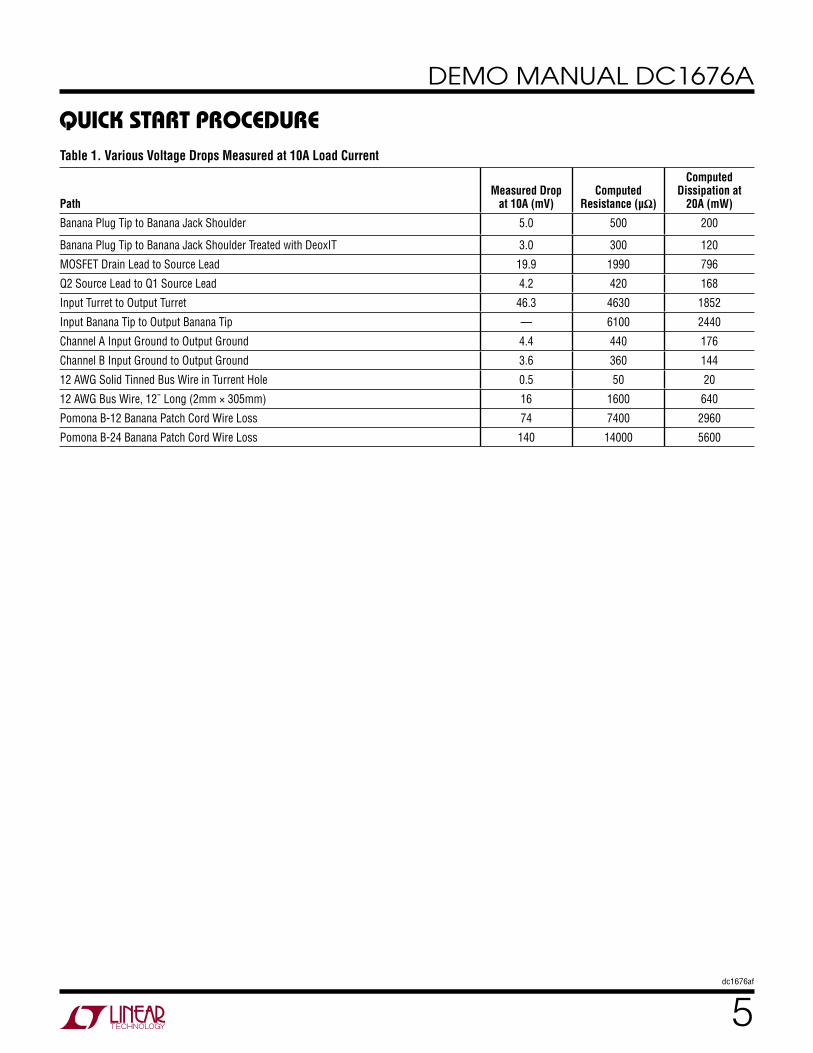
Table 1 summarizes various circuit resistances and as-sociated voltage and power losses.
ON/OFF Control
The LTC4359 may be turned on and off by placing the SHDN jumper in the ON or OFF position. In the OFF position the SHDN pin is connected to VSS through 100kΩ (R5), switch (Q2) is turned off, and the quiescent current is reduced to ≈14μA. In the ON position the SHDN pin floats allow-ing an internal 2μA pull up to assert it high, enabling the LTC4359. If the input is higher than the output, Q1 and Q2 are driven on; otherwise they remain off until forward current flow is possible.
In the EXT position, the SHDN pin is connected through R5 to the SHDN turret. If the SHDN turret is left open, the LTC4359 is enabled. To turn off, connect the SHDN turret to the neighboring VSS turret. SHDN pin level shift circuits are shown in data sheet Figure 3.
Because the SHDN pin is high impedance, it is subject to capacitive coupling. Pads are provided for an optional noise bypass capacitor, CF. R5 is included both for filter-ing and to help protect the SHDN pin against overvoltage conditions that might arise from use of the SHDN turret.
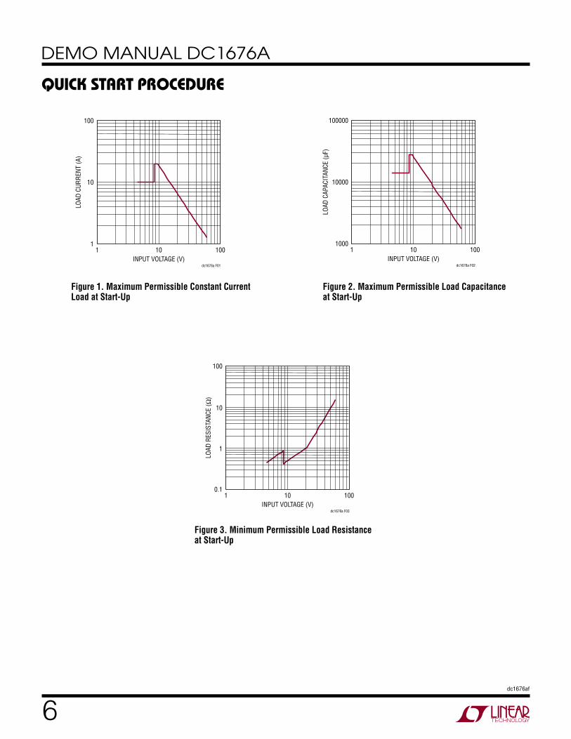
Load Limitations at Start-Up
Owing to its limited safe operating area (SOA), Q2 can be damaged if the output is heavily loaded at start-up. Start-up means activating the LTC4359 by abrupt application of power, or by asserting SHDN high. Figures 1, 2 and 3 show how much load can be supported at start-up, as a function of supply voltage for constant current, capacitive and resistive loads. The start-up capability is also a func-tion of slew rate, which is set by C1 to 714V/s.
Figure 1 shows how much load current can be started, assuming that the load current is constant over the entire start-up interval. As an example, at 28V do not attempt to drag up a constant current load of more than 3.5A. Current capability increases in direct proportion to the square root of slew rate.
Load capacitors draw a constant current in direct propor-tion to output slew rate. Figure 2 shows how much load capacitance can be safely driven at start-up as a function of input voltage. The capacitance is proportional to the reciprocal of the square root of slew rate.
Resistive loads, probably more common in the lab than in application, are less stressful than constant current loads because the current for large values of VDS is small, and VDS is small for large currents. Figure 3 shows minimum permissible load resistance as a function of input volt-age. As was the case for capacitive loads, the amount of resistance that can be safely started varies in proportion to the reciprocal of the square root of slew rate.
Figures 1, 2 and 3 apply for a P2t of 160W2s, loads that are present right from the onset of start-up, C1=10nF, and account for the effect of MOSFET capacitance which slows the slew rate to approximately 714V/s. Each graph presumes that the loading is exclusive: there is no other loading at start-up other than that suggested in the graph. Each graph also presumes that the output voltage starts from zero, and is not held up by a diode-OR arrangement. Discontinuities in the graphs arise because the loading is sometimes limited by the maximum permissible load cur-rent of 10A over the 4.5V to 8.5V range and 20A over the 8.5V to 60V range, and in other cases limited by Q2’s SOA.
Exact SOA analysis of a more complex loading situation, such as a mixture of constant current, resistive and ca-pacitive loading, is best quantified by simulation on a case by case basis. SOA is not an issue at turn off as the fall time is less than 1ms, in contrast to the rise time which approaches 85ms at 60V.
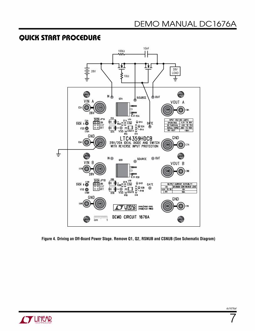
Modifying for Higher Current
An off-board power stage may be constructed and con-nected to DC1676A by using the IN, OUT, SOURCE and GATE test pads, provided Q1, Q2, CSNUB and RSNUB are removed from the DC1676A circuit board (see Figure 4). Snub the off-board MOSFETs with a 100Ω, 10nF series
Quick start proceDure
4dc1676af
DEMO MANUAL DC1676A
network. The off-board Q2 must have a 10Ω series resis-tor located at its gate lead, to prevent destructive parasitic oscillations. Keep the leads as short as possible, paying particular attention to GATE and SOURCE. Do not pass load current through the DC1676A ground terminals.
Modifying for Other Applications
Pads are provided for a SHDN pin filter capacitor, CF. This is useful for controlling the timing of ON/OFF signals, and for filtering noise if long wires are connected to the SHDN turret. Pads are also provided for D3, allowing the demo board to be modified to match certain data sheet applications.
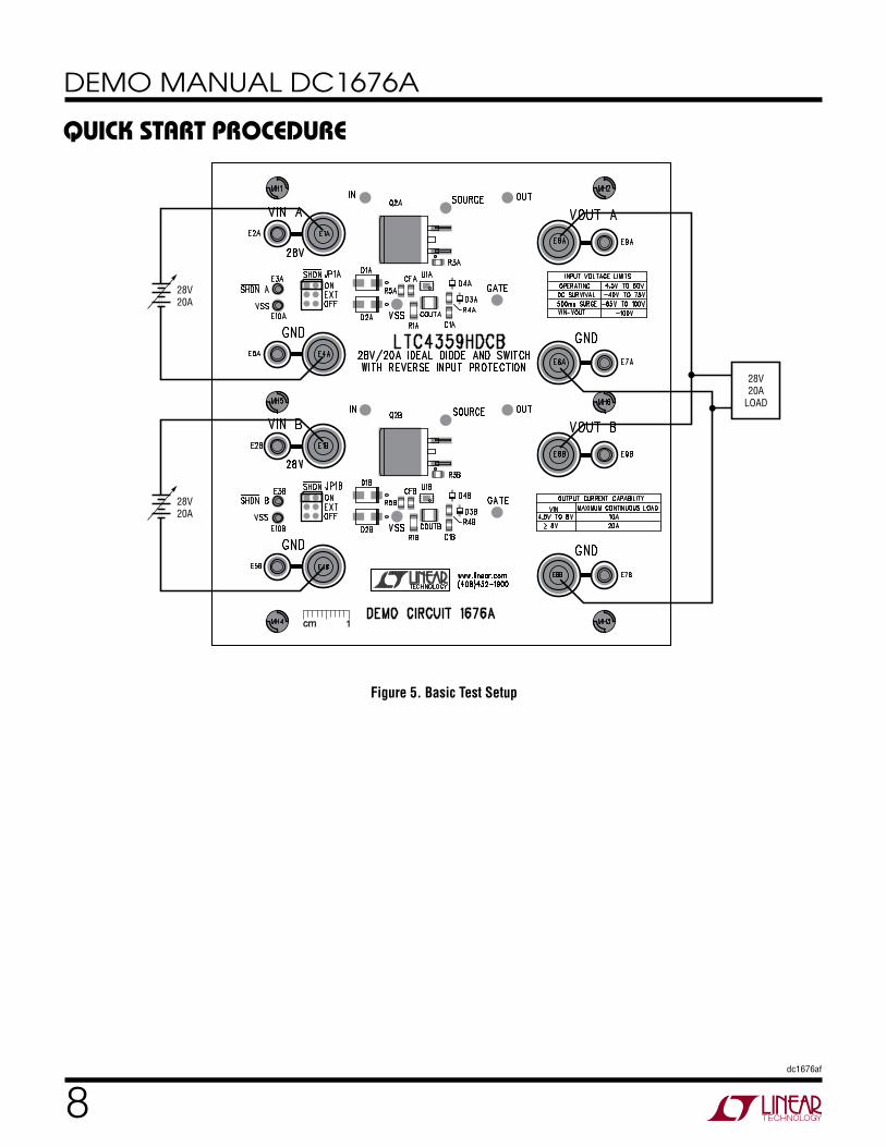
How to Operate DC1676A
A simple demonstration of DC1676A’s operation is as follows (see Figure 5). Connect two adjustable power sup-plies, each set to 28V. Connect one to VIN A and nearby GND, the second to VIN B and its associated GND. Place the SHDN jumpers in the ON position. Join together the outputs of VOUT A and VOUT B at the input of a DC load of up to 20A. Slowly adjust one power supply up and down relative to the other while monitoring the power supply currents. The higher supply will carry the load current, with a narrow transition region where the voltages are nearly identical and the supplies droop share. If one supply is shorted, the output voltage will not collapse—the other supply will carry the load.
Each channel can be individually controlled by its associated SHDN jumper. For example, if channel A is adjusted to 33V and channel B is set to 28V, channel A will supply the full load current. If channel A’s SHDN jumper is subsequently set to OFF, channel A will turn off and the full load current will be provided by channel B. This, of course, assumes that the outputs VOUT A and VOUT B are connected together as described in the previous paragraph.
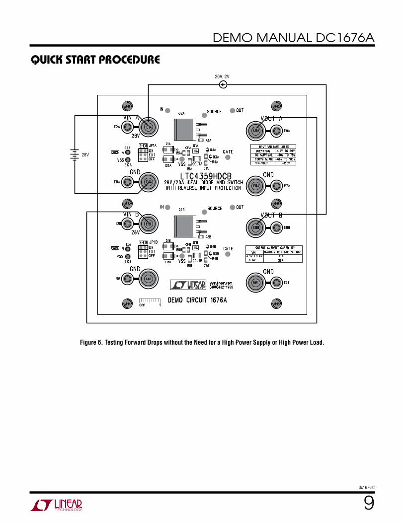
The forward characteristics of the LTC4359 can be tested without using a high power load and using only a low volt-age 20A supply, as shown in Figure 6. First, bias DC1676A with a 28V supply. This supply provides quiescent current for the two channels, totaling less than 1mA. Second, connect the two channels in series (VOUT A connected to VIN B), and connect a 20A, current-limited low voltage (1V to 2V) supply to VIN A and VOUT B.
Turn on the two supplies. 20A will flow from the input of channel A, through Q2A and Q1A, to the input of channel B, through Q2B and Q1B, and back out to the 20A power supply. This arrangement eliminates the need for high-power supplies or a high power load, yet the forward behavior of the LTC4359 and the board, connector and MOSFET voltage drops can be examined as though the board was fully loaded with each channel carrying 20A.
The 20A supply may be adjusted from zero to 20A and the 28V supply may be adjusted from 8.5V to 60V, to observe operation under any condition. At 10A, the 28V supply may be adjust to as low as 4.5V.
Quick start proceDure
5dc1676af
DEMO MANUAL DC1676A
Table 1. Various Voltage Drops Measured at 10A Load Current
PathMeasured Drop
at 10A (mV)Computed
Resistance (µΩ)
Computed Dissipation at
20A (mW)
Banana Plug Tip to Banana Jack Shoulder 5.0 500 200
Banana Plug Tip to Banana Jack Shoulder Treated with DeoxIT 3.0 300 120
MOSFET Drain Lead to Source Lead 19.9 1990 796
Q2 Source Lead to Q1 Source Lead 4.2 420 168
Input Turret to Output Turret 46.3 4630 1852
Input Banana Tip to Output Banana Tip — 6100 2440
Channel A Input Ground to Output Ground 4.4 440 176
Channel B Input Ground to Output Ground 3.6 360 144
12 AWG Solid Tinned Bus Wire in Turrent Hole 0.5 50 20
12 AWG Bus Wire, 12¨ Long (2mm × 305mm) 16 1600 640
Pomona B-12 Banana Patch Cord Wire Loss 74 7400 2960
Pomona B-24 Banana Patch Cord Wire Loss 140 14000 5600
Quick start proceDure
6dc1676af
DEMO MANUAL DC1676A
Quick start proceDure
INPUT VOLTAGE (V)
LOAD
CUR
RENT
(A)
dc1676a F01
100
10
11 10 100
INPUT VOLTAGE (V)
LOAD
RES
ISTA
NCE
(Ω)
dc1676a F03
100
1
10
0.11 10 100
Figure 1. Maximum Permissible Constant Current Load at Start-Up
Figure 2. Maximum Permissible Load Capacitance at Start-Up
Figure 3. Minimum Permissible Load Resistance at Start-Up
INPUT VOLTAGE (V)
LOAD
CAP
ACIT
ANCE
(µF)
dc1676a F02
100000
10000
10001 10 100
7dc1676af
DEMO MANUAL DC1676A
Quick start proceDure
Figure 4. Driving an Off-Board Power Stage. Remove Q1, Q2, RSNUB and CSNUB (See Schematic Diagram)
10Ω
100Ω
28VLOAD28V
10nF
8dc1676af
DEMO MANUAL DC1676A
Quick start proceDure
28V20A
28V20A
28V20A
LOAD
Figure 5. Basic Test Setup
9dc1676af
DEMO MANUAL DC1676A
Quick start proceDure20A, 2V
28V
Figure 6. Testing Forward Drops without the Need for a High Power Supply or High Power Load.
10dc1676af
DEMO MANUAL DC1676A
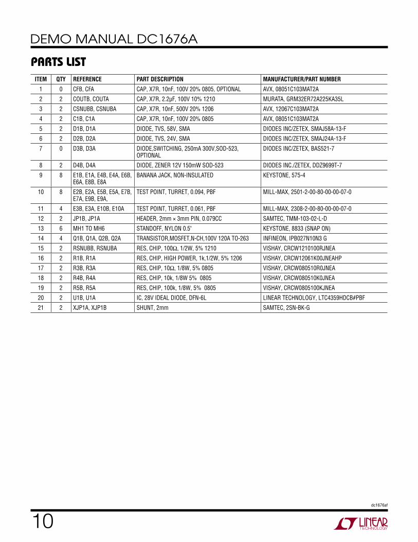
parts ListITEM QTY REFERENCE PART DESCRIPTION MANUFACTURER/PART NUMBER
1 0 CFB, CFA CAP, X7R, 10nF, 100V 20% 0805, OPTIONAL AVX, 08051C103MAT2A
2 2 COUTB, COUTA CAP, X7R, 2.2µF, 100V 10% 1210 MURATA, GRM32ER72A225KA35L
3 2 CSNUBB, CSNUBA CAP, X7R, 10nF, 500V 20% 1206 AVX, 12067C103MAT2A
4 2 C1B, C1A CAP, X7R, 10nF, 100V 20% 0805 AVX, 08051C103MAT2A
5 2 D1B, D1A DIODE, TVS, 58V, SMA DIODES INC/ZETEX, SMAJ58A-13-F
6 2 D2B, D2A DIODE, TVS, 24V, SMA DIODES INC/ZETEX, SMAJ24A-13-F
7 0 D3B, D3A DIODE,SWITCHING, 250mA 300V,SOD-523, OPTIONAL
DIODES INC/ZETEX, BAS521-7
8 2 D4B, D4A DIODE, ZENER 12V 150mW SOD-523 DIODES INC./ZETEX, DDZ9699T-7
9 8 E1B, E1A, E4B, E4A, E6B, E6A, E8B, E8A
BANANA JACK, NON-INSULATED KEYSTONE, 575-4
10 8 E2B, E2A, E5B, E5A, E7B, E7A, E9B, E9A,
TEST POINT, TURRET, 0.094, PBF MILL-MAX, 2501-2-00-80-00-00-07-0
11 4 E3B, E3A, E10B, E10A TEST POINT, TURRET, 0.061, PBF MILL-MAX, 2308-2-00-80-00-00-07-0
12 2 JP1B, JP1A HEADER, 2mm × 3mm PIN, 0.079CC SAMTEC, TMM-103-02-L-D
13 6 MH1 TO MH6 STANDOFF, NYLON 0.5" KEYSTONE, 8833 (SNAP ON)
14 4 Q1B, Q1A, Q2B, Q2A TRANSISTOR,MOSFET,N-CH,100V 120A TO-263 INFINEON, IPB027N10N3 G
15 2 RSNUBB, RSNUBA RES, CHIP, 100Ω, 1/2W, 5% 1210 VISHAY, CRCW1210100RJNEA
16 2 R1B, R1A RES, CHIP, HIGH POWER, 1k,1/2W, 5% 1206 VISHAY, CRCW12061K00JNEAHP
17 2 R3B, R3A RES, CHIP, 10Ω, 1/8W, 5% 0805 VISHAY, CRCW080510R0JNEA
18 2 R4B, R4A RES, CHIP, 10k, 1/8W 5% 0805 VISHAY, CRCW080510K0JNEA
19 2 R5B, R5A RES, CHIP, 100k, 1/8W, 5% 0805 VISHAY, CRCW0805100KJNEA
20 2 U1B, U1A IC, 28V IDEAL DIODE, DFN-6L LINEAR TECHNOLOGY, LTC4359HDCB#PBF
21 2 XJP1A, XJP1B SHUNT, 2mm SAMTEC, 2SN-BK-G
11dc1676af
DEMO MANUAL DC1676A
Information furnished by Linear Technology Corporation is believed to be accurate and reliable. However, no responsibility is assumed for its use. Linear Technology Corporation makes no representa-tion that the interconnection of its circuits as described herein will not infringe on existing patent rights.
schematic Diagram
12dc1676af
DEMO MANUAL DC1676A
Linear Technology Corporation1630 McCarthy Blvd., Milpitas, CA 95035-7417 (408) 432-1900 ● FAX: (408) 434-0507 ● www.linear.com LINEAR TECHNOLOGY CORPORATION 2013
LT 0313 • PRINTED IN USA
DEMONSTRATION BOARD IMPORTANT NOTICE
Linear Technology Corporation (LTC) provides the enclosed product(s) under the following AS IS conditions:
This demonstration board (DEMO BOARD) kit being sold or provided by Linear Technology is intended for use for ENGINEERING DEVELOPMENT OR EVALUATION PURPOSES ONLY and is not provided by LTC for commercial use. As such, the DEMO BOARD herein may not be complete in terms of required design-, marketing-, and/or manufacturing-related protective considerations, including but not limited to product safety measures typically found in finished commercial goods. As a prototype, this product does not fall within the scope of the European Union directive on electromagnetic compatibility and therefore may or may not meet the technical requirements of the directive, or other regulations.
If this evaluation kit does not meet the specifications recited in the DEMO BOARD manual the kit may be returned within 30 days from the date of delivery for a full refund. THE FOREGOING WARRANTY IS THE EXCLUSIVE WARRANTY MADE BY THE SELLER TO BUYER AND IS IN LIEU OF ALL OTHER WARRANTIES, EXPRESSED, IMPLIED, OR STATUTORY, INCLUDING ANY WARRANTY OF MERCHANTABILITY OR FITNESS FOR ANY PARTICULAR PURPOSE. EXCEPT TO THE EXTENT OF THIS INDEMNITY, NEITHER PARTY SHALL BE LIABLE TO THE OTHER FOR ANY INDIRECT, SPECIAL, INCIDENTAL, OR CONSEQUENTIAL DAMAGES.
The user assumes all responsibility and liability for proper and safe handling of the goods. Further, the user releases LTC from all claims arising from the handling or use of the goods. Due to the open construction of the product, it is the user’s responsibility to take any and all appropriate precautions with regard to electrostatic discharge. Also be aware that the products herein may not be regulatory compliant or agency certified (FCC, UL, CE, etc.).
No License is granted under any patent right or other intellectual property whatsoever. LTC assumes no liability for applications assistance, customer product design, software performance, or infringement of patents or any other intellectual property rights of any kind.
LTC currently services a variety of customers for products around the world, and therefore this transaction is not exclusive.
Please read the DEMO BOARD manual prior to handling the product. Persons handling this product must have electronics training and observe good laboratory practice standards. Common sense is encouraged.
This notice contains important safety information about temperatures and voltages. For further safety concerns, please contact a LTC applica-tion engineer.
Mailing Address:
Linear Technology
1630 McCarthy Blvd.
Milpitas, CA 95035
Copyright © 2004, Linear Technology Corporation