Embed Size (px)
Citation preview
www.ijecs.in International Journal Of Engineering And Computer Science ISSN:2319-7242 Volume 2 Issue 11 November, 2013 Page No. 3250-3255
Sree Vardhan IJECS Volume 2 Issue 11 November, 2013 Page No. 3250-3255 Page 3250
DC/DC Boost Converter Functionality in a Three-Phase IMC
Sree Vardhan, S.V. Panidhar
Abstract—An indirect matrix converter (IMC) connected with two input power sources is proposed: a gasoline generator
as themain ac power supply and batteries as the secondary power source. The IMC is small in size because of having a dc-
link part without an electrolytic capacitor. The dc-link part is utilized by connection with a boost-up chopper with
batteries as a secondary input power source. Furthermore, the chopper connects to the neutral point of the motor and
utilizes the leakage inductance of the motor as a reactor component. The proposed technique successfully further reduce
the size of the converter by removing the boost reactor in the boost converter stage. The proposed converter is simulated
and experimentally validated using a 750-W prototype and an induction motor driven with V/f control. The total harmonic
distortion of the input and output currents are 4% and 3.7%, respectively,and the efficiency is 96%
Index terms—Synchronous Reference Frame,
instantaneous current component theory, Modified SRF,
Active Filter, Harmonics.
I. INTRODUCTION
Environmental responsibility has become a significant
concern for communities so that the development of
renewable power sources, such as wind turbines and low-
carbon emission hybrid electric vehicles (HEVs) is
progressing rapidly. One of the most common applied
converters in hybrid systems is the ac/dc/ac converter
because it has the ability of connecting to two different
power sources. The generator mainly supplies constant
power to the load and a battery is used as an alternate power
source to drive an electric motor and also to absorb the
power fluctuation during periods of high peak energy
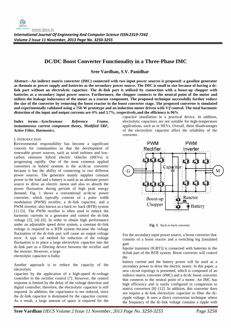
demand. Fig. 1 shows a conventional ac/dc/ac power
converter, which typically consists of a pulse width
modulation (PWM) rectifier, a dc-link capacitor, and a
PWM inverter, also known as a back to- back (BTB) system
[1]–[3]. The PWM rectifier is often used to reduce the
harmonic currents in a generator and control the dc-link
voltage [2], [4]–[6]. In order to obtain high performance
under an adjustable speed drive system, a constant dc-link
voltage is required in a BTB system because the voltage
fluctuation of the dc-link part will cause an output voltage
error. A typi- cal method for reduction of the voltage
fluctuation is to place a large electrolytic capacitor into the
dc-link part as a filtering device between the rectifier and
the inverter. However, a large
electrolytic capacitor is bulky
Another approach is to reduce the capacity of the
electrolytic
capacitor by the application of a high-speed dc-voltage
controller to the rectifier control [7]. However, the control
response is limited by the delay of the voltage detection and
digital controller; therefore, the electrolytic capacitor is still
required. In addition, the capacitance is not reduced, since
the dc-link capacitor is dominated by the capacitor current.
As a result, a large amount of space is required for the
capacitor installation in a practical device. In addition,
electrolytic capacitors are not suitable for high-temperature
applications, such as in HEVs. Overall, these disadvantages
of the electrolytic capacitor affect the reliability of the
converter.
.
Fig. 1: Back-to-back converter.
For the secondary input power source, a boost converter that
consists of a boost reactor and a switching leg [insulated
gate
bipolar transistor (IGBT)] is connected with batteries to the
dclink part of the BTB system. Boost converter will control
the
battery current and the battery power will be used as a
secondary power to drive the electric motor. In this paper, a
new circuit topology is presented, which is composed of an
indirect matrix converter (IMC) and a dc/dc boost converter
that connects to the neutral point of a motor. An IMC has
high efficiency and is easily configured in comparison to
matrix converters [8]–[12]. In addition, this converter does
not require a dc-link electrolytic capacitor to filter the dc-
ripple voltage. It uses a direct conversion technique where
the frequency of the dc-link voltage contains a ripple with
Sree Vardhan IJECS Volume 2 Issue 11 November, 2013 Page No. 3250-3255 Page 3251
six times of the input frequency. However, the output
voltage transfer ratio is limited by this direct conversion
technique which is similar to the matrix converter, where
output voltage = 0.866 of the input voltage [13].1)
Where x denotes voltages or currents.
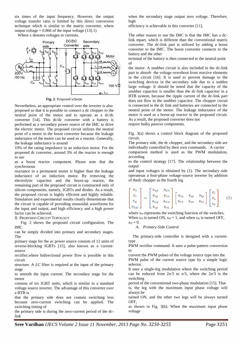
Fig. 2: Proposed scheme
Nevertheless, an appropriate control over the inverter is also
proposed so that it is possible to connect a dc chopper to the
neutral point of the motor and to operate as a dc/dc
converter [14]. This dc/dc converter with a battery is
performed as a secondary power source of the IMC to drive
the electric motor. The proposed circuit utilizes the neutral
point of a motor in the boost converter because the leakage
inductance of the motor can be used as a reactor. Generally,
the leakage inductance is around
10% of the rating impedance in an induction motor. For the
proposed dc converter, around 3% of the reactor is enough
to use
as a boost reactor component. Please note that the
synchronous
reactance in a permanent motor is higher than the leakage
inductance of an induction motor. By removing the
electrolytic capacitor and the boost-up reactor, the
remaining part of the proposed circuit is constructed only of
silicon components, namely, IGBTs and diodes. As a result,
the proposed circuit is highly efficient and highly reliable.
Simulation and experimental results clearly demonstrate that
the circuit is capable of providing sinusoidal waveforms for
the input and output, and high efficiency and a high power
factor can be achieved.
II. PROPOSED CIRCUIT TOPOLOGY
Fig. 2 shows the proposed circuit configuration. The
IMC
can be simply divided into primary and secondary stages.
The
primary stage for the ac power source consists of 12 units of
reverse-blocking IGBTs [15], also known as a current-
source
rectifier,where bidirectional power flow is possible in this
circuit
structure. A LC filter is required at the input of the primary
stage
to smooth the input current. The secondary stage for the
motor
consists of six IGBT units, which is similar to a standard
voltage source inverter. The advantage of this converter over
a BTB is
that the primary side does not contain switching loss
because zero-current switching can be applied. The
switching timing of
the primary side is during the zero-current period of the dc-
link
when the secondary stage output zero voltage. Therefore,
high
efficiency is achievable in this converter [11].
The other reason to use the IMC is that the IMC has a dc-
link mpart, which is different than the conventional matrix
converter. The dc-link part is utilized by adding a boost
converter to the IMC. The boost converter connects to the
battery and the other
terminal of the battery is then connected to the neutral point
of
the motor. A snubber circuit is also included in the dc-link
part to absorb the voltage overshoot from reactive elements
in the circuit [16]. It is used to prevent damage to the
switching devices in the secondary side due to a sudden
large voltage. It should be noted that the capacity of the
snubber capacitor is smaller than the dc-link capacitor in a
BTB system, because the ripple current of the dc-link part
does not flow in the snubber capacitor. The chopper circuit
is connected in the dc link and batteries are connected to the
neutral point of the motor. The leakage inductance of the
motor is used as a boost-up reactor in the proposed circuit.
As a result, the proposed converter does not
require bulky passive components.
Fig. 3(a) shows a control block diagram of the proposed
circuit.
The primary side, the dc chopper, and the secondary side are
individually controlled by their own commands. A carrier
comparison method is used as the PWM modulation,
according
to the control strategy [17]. The relationship between the
output
and input voltages is obtained by (1). The secondary side
operatesas a four-phase voltage-source inverter by addition
of thedc chopper as the fourth leg
where sxy represents the switching function of the switches.
When sxy is turned ON, sxy = 1, and when sxy is turned OFF,
sxy = 0.
A. Primary-Side Control
The primary-side controller is designed with a current-
type
PWM rectifier command. It uses a pulse-pattern conversion
to
convert the PWM pulses of the voltage source type into the
PWM pulse of the current source type by a simple logic
selector.
It uses a single-leg modulation where the switching period
can be reduced from 2π/3 to π/3, where the 2π/3 is the
switching
period of the conventional two-phase modulation [15]. That
is, the leg with the maximum input phase voltage will
always be
turned ON, and the other two legs will be always turned
OFF,
as shown in Fig. 3(b). When the maximum input phase
voltage
Sree Vardhan IJECS Volume 2 Issue 11 November, 2013 Page No. 3250-3255 Page 3252
is changing, (for example, from +R-phase to −S-phase), the
related max phase voltage leg and the mid phase voltage leg
will
be switched at zero current until the relevant switch that
contains
the mid phase voltage becomes the maximum input phase
voltage. From this direct conversion technique, a dc-link
voltage
that contains a ripple with six times of the input frequency
will
be formed [15].
B. Secondary-Side Control
A conventional controller method for a voltage-source-
type
inverter is applied to the dc chopper and the inverter with a
lean
controlled carrier modulation. The carrier modulation forms
a
Fig. 3 (a) Control block diagram. (b) Primary-side-switching
pattern
new carrier, where the peak position of the triangular
carrier
is controlled by the duty ratio of the rectifier-side pulse. This
rectifier pulse is used to control the switching timing of the
primary stage and the zero-vector of the secondary stage.
From
the control, zero-current switching is achieved in the
primary
stage, where the dc-link current becomes zero at the peak of
every carrier. This new carrier is then used in the secondary
side
and the dc chopper side as a normal PWM comparison
method,
also referred to as an inverter carrier.
The boost converter is not a stand-alone circuit in the
proposed circuit. Operation is strongly dependent on the
secondary side of the IMC. Zero-vector outputs on the
secondary side are the key factor to link the boost converter
to the IMC. The zero vector controls the amplitude of the
output voltage. There are two functions of the zero-vector
output to the secondary side. The first is to implement zero-
current switching on the primary side so that the switching
losses do not occur at the primary side. The second function
involves operation of the boost converter, which will be
described in a later chapter.Fig. 4 shows an example of the
relationship between the normal carrier applied to the
primary side and the new inverter carrier applied to the
secondary side.
The inverter commands are given by the voltage controller
as described in Chapter IV. It is noted that the dc chopper is
controlled as the fourth leg of the inverter so that the dc
chopper command is compared by the same carrier with the
inverter voltage commands. There are two methods to
generate an inverter carrier; Fig. 4(a) represents the
symmetrical type, which has approximately double the
switching frequency of the rectifier switching frequency,
and Fig. 4(b) shows the asymmetrical type, which has the
same switching frequency as the rectifier switching
frequency [16]. min Fig. 4(a), the bottom peak position of
the triangular carrier is controlled by the duty ratio of the
rectifier pulse, as shown in
.
Fig. 4. Relationship between the zero vectors and boost converter
operation. (a) Symmetrical inverter carrier. (b) Asymmetrical inverter carrier
the upper part of the figure. The chopper commands, along
with
the inverter output voltage commands, are compared with
this
new inverter carrier to obtain the desired switching patterns.
The
zero-vector periods are shown in the lower part of Fig. 4(a).
The
switching pulses of the secondary side attain the zero
vectors
for every carrier cycle. The primary side arms switch at
every
zero-vector period.
In Fig. 4, zv_u and zv_l represent the zero-vector periods of
the inverter, where zv u = Sup = Svp = Swp = 1 (upper arm
zero vector) and zv l = Sup = Svp = Swp = 0[lower arm zero
vector (Sun = Svn = Swn = 1)]. The upper arm of the chopper
(Scp) switches ON at every zero-vector period of zv_u. On
the
Other hand, the lower arm of the chopper (Scn ) will switch
ON
Sree Vardhan IJECS Volume 2 Issue 11 November, 2013 Page No. 3250-3255 Page 3253
at every zero-vector periods of zv_l. During these zero-
vector
periods, the boost converter is operated in the ON-state, and
the battery current through the leakage inductance of the
motor
increases. During the nonzero-vector periods, also known as
the OFF-state operation, the battery current is released into
the
capacitor in the LC filter at the power source. The operation
state in the figure is referred to the boost converter
operation.
When the switching frequency of the rectifier is 10 kHz, the
control method applied in Fig. 4(a) generates a new
symmetrical
carrier that has a frequency of approximately 20 kHz. This
is approximately twice the primary-side switching
frequency.
Alternatively, according to Fig. 4(b), an inverter carrier can
be
formed based on the duty of the rectifier command, which is
asymmetrical with a frequency of 10 kHz
By comparing the symmetrical and asymmetrical
inverter carriers in Fig. 4, it should be noted that the zero-
current n switching in the rectifier is not affected by the
inverter carrier because
both carriers are formed following the rectifier duty. Since
every
carrier time is longer in the asymmetrical inverter carrier,
the
sequence of the zero-vector periods becomes slower;
therefore,
the boost converter will achieve better efficiency, but the
current
ripple in the battery will be increased. Further, the
asymmetrical
method can achieve better total harmonic distortion (THD)
values for the output because the deadtime effect is smaller
due
to the lower switching frequency. The other disadvantage of
the asymmetrical inverter carrier is the detection of the load
current. Usually, the average value of the load current
appears at the peak of the symmetrical inverter carrier so
that it can be easily detected using the symmetrical inverter
carrier. However, for the asymmetrical carrier, the average
current point does not agree with the peak of the
asymmetrical carrier; therefore, in order to detect the
average current, a lowpass filter is required. Consequently,
control performance will be decreased.
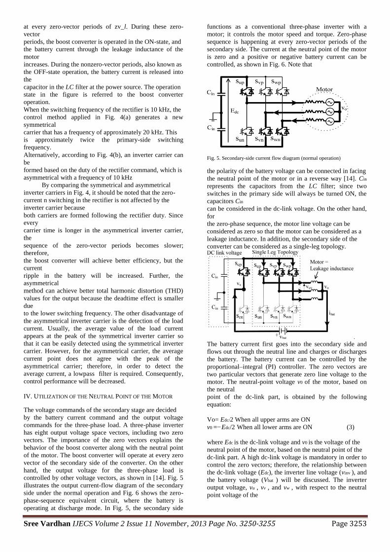
IV. UTILIZATION OF THE NEUTRAL POINT OF THE MOTOR
The voltage commands of the secondary stage are decided
by the battery current command and the output voltage
commands for the three-phase load. A three-phase inverter
has eight output voltage space vectors, including two zero
vectors. The importance of the zero vectors explains the
behavior of the boost converter along with the neutral point
of the motor. The boost converter will operate at every zero
vector of the secondary side of the converter. On the other
hand, the output voltage for the three-phase load is
controlled by other voltage vectors, as shown in [14]. Fig. 5
illustrates the output current-flow diagram of the secondary
side under the normal operation and Fig. 6 shows the zero-
phase-sequence equivalent circuit, where the battery is
operating at discharge mode. In Fig. 5, the secondary side
functions as a conventional three-phase inverter with a
motor; it controls the motor speed and torque. Zero-phase
sequence is happening at every zero-vector periods of the
secondary side. The current at the neutral point of the motor
is zero and a positive or negative battery current can be
controlled, as shown in Fig. 6. Note that
Fig. 5. Secondary-side current flow diagram (normal operation)
the polarity of the battery voltage can be connected in facing
the neutral point of the motor or in a reverse way [14]. Cin
represents the capacitors from the LC filter; since two
switches in the primary side will always be turned ON, the
capacitors Cin
can be considered in the dc-link voltage. On the other hand,
for
the zero-phase sequence, the motor line voltage can be
considered as zero so that the motor can be considered as a
leakage inductance. In addition, the secondary side of the
converter can be considered as a single-leg topology.
. The battery current first goes into the secondary side and
flows out through the neutral line and charges or discharges
the battery. The battery current can be controlled by the
proportional–integral (PI) controller. The zero vectors are
two particular vectors that generate zero line voltage to the
motor. The neutral-point voltage v0 of the motor, based on
the neutral
point of the dc-link part, is obtained by the following
equation:
Vo= Edc/2 When all upper arms are ON
v0 =−Edc/2 When all lower arms are ON (3)
where Edc is the dc-link voltage and v0 is the voltage of the
neutral point of the motor, based on the neutral point of the
dc-link part. A high dc-link voltage is mandatory in order to
control the zero vectors; therefore, the relationship between
the dc-link voltage (Edc), the inverter line voltage (vinv ), and
the battery voltage (Vbat ) will be discussed. The inverter
output voltage, vu , vv , and vw , with respect to the neutral
point voltage of the

Sree Vardhan IJECS Volume 2 Issue 11 November, 2013 Page No. 3250-3255 Page 3254
dc link, is expressed as
vu = aEdc/2sin ωt + v0
vv = aEdc/2(sinωt − 2π3)+ v0
vw = aEdc/2(sinωt − 4π3)+ v0 (3)
where a is the modulation index of the motor phase voltage,
0 <
a < 1, v0 is the neutral point voltage of the motor (during
zero
phase sequence), and ω is the inverter output angular
frequency.
The inverter line voltage is then given by (u–v phase)
vuv = a√3/2 Edc sin_(ωt + π/6) (4)
Equation (5) shows the relationship for an inverter to obtain
the maximum output line voltage Vinv (rms) under the
maximum
reference magnitude of a three-phase modulation
Edc ≥ 2√2 /√3Vinv . (5)
The maximum line voltage between the inverter leg and
chopper
leg can be obtained as (rms)
vux =√2/ √3Vinv + Vbat (6)
Since vux must be smaller than Edc, the inverter voltage and
battery voltage are constrained by the following equation
Edc >√2/ √3Vinv + Vbat (7)
As a result, the dc-link voltage of the proposed circuit must
satisfy both requirements as shown by the following
equation,
which can be referring to Fig. 6
Note that in (8), the Vbat can always be neutralized with half
of the Edc under the two conditions. That is, Vbat must be
always
smaller than half of the Edc, since the Edc is always known
as
the 0.866 of the input phase voltage, as shown in the
following
equation
√2/2 Vin0.866 > Vbat (9)
Furthermore, a new expression of the secondary-side
current
is given as follows, assuming that the leakage impedance is
even
during the zero-phase-sequence equivalent circuit
iu = ia + ibat/3 iv = ib + ibat/3 iw = ic + ibat/3 (10) where iu , iv , and iw are the inverter currents, ia , ib , and ic are
the
positive-phase-inverter current, and ibat is the battery current
V. SIMULATION RESULTS
Table I shows the simulation parameters for both results.
The
proposed circuit was simulated under two conditions of
battery
discharge and charge. An automatic current regulator (ACR)
ncontroller controls the battery current to a desired positive
or negative value. An ideal battery current ibat is purposely
adjusted
at a specific time of 38 ms to confirm the proposed circuit
performance. The motor model, which consists of three sets
of
voltage sources as back-electromotive forces and leakage
inductances, is used in the simulation. The asymmetrical
inverter
carrier was used in the simulation. Fig. 7 shows the battery
discharge mode, with the battery current controlled from 0.5
to 2 A. The two waveforms show the input power supply
voltages vr , vs , and vt , the input currents ir , is , and it , and
the output line voltages (vuv(LPF) , vvw(LPF) , and vwu(LPF) )
through a low-pass filter, which has a cutoff frequency of 1
kHz, to observe the low-frequency components, the output
currents iu , iv , and iw , and the battery current ibat . The
results show that the THD of both the input and output
currents are less than 4%. It should be noted that at 20 ms,
the input current magnitude decreases due to the increment
of ibat , which indicates that the increase of the battery power
leads to a decrease in generator power. On the other hand,
Fig. 8 shows the ACR controlling the battery current from
0.5 to −2 A. The battery is charged from a generator under
this condition. The results also showed that when in the
charging mode, both the input and output currents have
good sinusoidalwaveforms. At 20 ms, as the ibat decreases,
the input current is forced to increase, because higher power
is required to charge the battery. These two waveforms
provide evidence of good power management between the
generator and the battery.
i/p voltage,i/p current,o/p voltage,o/p current,battery current

Sree Vardhan IJECS Volume 2 Issue 11 November, 2013 Page No. 3250-3255 Page 3255
Fig. 7. Simulation results (battery = discharge mode).
i/p voltage,i/p current,o/p voltage,o/p current,battery current
Fig. 8 Simulation results (battery = charge mode)
VII. CONCLUSION
A new control method is proposed by utilizing the neutral
point of a motor and connection to an IMC for motor drive
applications. Control over the inverter zero-vector periods
allows an additional chopper leg to perform as a boost
converter
with connection to the neutral point of a motor. Simulation
results demonstrated good sinusoidal waveforms and
confirmed the validity of the proposed method.
REFERENCES
[1] D. Casadei, G. Grandi, C. Rossi, A. Trentin, and L. Zarri, “Comparison
between back-to-back and matrix converters based on thermal stress of
the switches,” in Proc. IEEE Int. Symp. Ind. Electron., May 2004, vol. 2, pp. 1081–1086.
[2] R. Ghosh and G. Narayanan, “Control of three-phase, four-wire PWM
rectifier,” IEEE Trans. Power Electron., vol. 23, no. 1, pp. 96–106, Jan. 2008.
[3] R. Lai, F. Wang, R. Burgos, Y. Pei, D. Boroyevich, B. Wang, T. A. Lipo,
V. D. Immanuel, and K. J. Karimi, “A systematic topology evaluation
methodology for high-density three-phase PWM AC-AC converters,”
IEEE Trans. Power Electron., vol. 23, no. 6, pp. 2665–2680, Nov. 2008.
[4] X. H.Wu, S. K. Panda, and J. X. Xu, “Analysis of the instantaneous
power flowfor three-phasePWMboost rectifier under unbalanced supply voltage
conditions,” IEEE Trans. Power Electron., vol. 23, no. 4, pp. 1679–1691,
Jul. 2008. [5] B. Yin, R. Oruganti, S. K. Panda, and A. K. S. Bhat, “A simple
singleinput-
single-output (SISO) model for a three-phasePWMrectifier,” IEEE Trans. Power Electron., vol. 24, no. 3, pp. 620–631, Mar. 2009.
[6] H.Yoo, J.-H.Kim, and S.-K. Sul, “Sensorless operation of
aPWMrectifier for a distributed generation,” IEEE Trans. Power Electron., vol. 22, no. 3,
pp. 1014–1018, May 2007.
[7] Y. Chen and X. Jin, “Modeling and control of three-phase voltage source
PWM rectifier,” in Proc. IEEE Power Electron. Motion Control Conf.,
Shanghai, Aug. 2006, vol. 3, pp. 1–4. [8] R.Vargas, U. Ammann, and J. Rodriguez, “Predictive approach to
increase
efficiency and reduce switching losses onmatrix converters,” IEEE Trans. Power Electron., vol. 24, no. 4, pp. 894–902, Apr. 2009.
[9] M. Jussila and H. Tuusa, “Comparison of simple control strategies of
space-vector modulated indirect matrix converter under distorted supply voltage,” IEEE Trans. Power Electron., vol. 22, no. 1, pp. 139–148, Jan.
2007.
[10] T. Friedli, M. L. Heldwein, F. Giezendanner, and J. W. Kolar, “A high
efficiency indirect matrix converter utilizing RB-IGBTs,” in Proc. 37th IEEE Power Electron. Spec. Conf., Jeju, Jun. 2006, pp. 1–7.
[11] J.W. Kolar, F. Schafmeister, S. D. Round, and H. Ertl, “Novel three-
phase AC–AC sparse matrix converters,” IEEE Trans. Power Electron., vol. 22,
no. 5, pp. 1649–1661, Sep. 2007.
[12] J.-I. Itoh and K.-I. Nagayoshi, “A new bidirectional switch with regenerative
snubber to realize a simple series connection for matrix converters,”
IEEE Trans. Power Electron., vol. 24, no. 3, pp. 822–829, Mar. 2009.
[13] T. Wijekoon, C. Klumpner, P. Zanchetta, and P. W. Wheeler,
“Implementation of a hybrid AC–AC direct power converter with unity voltage
transfer,” IEEE Trans. Power Electron., vol. 23, no. 4, pp. 1918–1926,
Jul. 2008. [14] J. Itoh and K. Fujita, “Novel unity power factor circuits using zero-
vector
control for single-phase input systems,” IEEE Trans. Power Electron., vol. 15, no. 1, pp. 36–43, Jan. 2000.
[15] J.-i. Itoh, I. Sato, A. Odaka, H. Ohguchi, H. Kodachi, and N. Eguchi,
“A novel approach to practical matrix converter motor drive system with reverse blocking IGBT,” IEEE Trans. Power Electron., vol. 20, no. 6,
pp. 1356–1363, Nov. 2005.
[16] K. Kato and J.-i. Itoh, “Control method for a three-port interface converter
using an indirect matrix converter with an active snubber circuit,” in Proc. 13th Power Electron. Motion Control Conf., Poznan, Sep. 2008, pp. 581–
588.
[17] J.-i. Itoh, S. Ikuya, O. Hideki, S. Kazuhisa, O. Akihiro, and E. Naoya, “A control method for the matrix converter based on virtual AC/DC/AC
conversion using carrier comparison method,” IEEJ Trans. Ind. Appl.,
vol. 152, no. 3, pp. 65–73, Jun. 2005. [18] J.-i Itoh, T. Iida, and A. Odaka, “Realization of high efficiency AC
link
converter system based on AC/AC direct conversion techniques with RBIGBT,”
in Proc. 32nd Ann. Conf. IEEE Ind. Electron., Paris, Nov. 2006,
pp. 1703–1708. [19] S. Round, F. Schafmeister, M. Heldwein, E. Pereira, L. Serpa, and
J. W. Kolar, “Comparison of performance and realization effort of a very
sparse matrix converter to a voltage dc link pwm inverter with active front end,” IEEJ Trans. Inst. Electr. Eng. Jpn., vol. 126-D, no. 5, pp. 578–588,
May 2006.