Embed Size (px)
Citation preview

By: ______________Class: ____________Roll No: __________
1

ACKNOWLEDGEMENT
I acknowledge the valuable contribution of Mr. Umesh Tyagi in providing me the proper guidance to complete these demonstration experiments. The experiments would not have been completed without his support and kind help. I would also be thankful of Mr. Satpal Singh (Physics Laboratory Assistant).
2
*********************
3

CERTIFICATE
This is to certify that ___________________, Roll number _______ of Class _____ has successfully completed the Demonstration Experiment under my supervision according to the guidelines laid down by CBSE.
Teacher Incharge Vice PrincipalPrincipal
4

5

CONTENTS
1) Demonstration Experiment 1_____________________________51.1) Aim1.2) Apparatus1.3) Principle1.4) Circuit Diagram1.5) Construction1.6) Working1.7) Description of parts
1.7.1) Step-Down Transformer1.7.2) p-n junction diode1.7.3) Capacitor1.7.4) Load Resistance
2) Demonstration Experiment 2____________________________152.1) Aim2.2) Apparatus2.3) Theory
2.3.1) Diffraction2.3.2) Diffraction through single slit (Graph)2.3.3) Diffraction through single slit (Pattern Observed)2.3.4) Single Slit Experiment2.3.5) Condition for Secondary Minima2.3.6) Condition for Secondary Maxima2.3.7) Width of Central Minima2.3.8) Width of Central Maxima2.3.9) Angular Width of Central Maxima2.3.10) Factors affecting width of Central Maxima
2.4) Observations2.5) Result
6

To construct a Full Wave Rectifier
7

TOutput d.c. Voltage
Input a.c. voltage
RL
P S
C
D
B
A
D1
D2
It is based on the principle that the diode offers low resistance when it is forward biased and offers high resistance when it is reverse biased.
The a.c. supply is fed across the primary coil P of a step down transformer. Two two ends of the secondary coil S of the transformer are connected to the p- regions of the junction diodes D1 and D2 . A load resistance RL is connected beteen the n-regions of the two diodes and the ncentral tapping of the secondary coil. The out put d.c. is obtained across the load reistance.
8

A.C. Input Voltage
D.C. 0utput Voltage
Suppose that during first half of the input, the upper end A of the secondary is at + ve pot. and lower end B is at (–) ve pot. So the diode D1 gets forward bias and D2 gets reverse bias hence current flows through D1 in load resistance from C to D. During the next half cycle A becomes –ve and B becomes +ve and hence D1 gets reverse bias and D2 gets forward bias. Thus the current flows through D2 from C to D in load resistance. Hence the full wave rectifier, rectifies the both halves of a.c. The output d.c. is continuous but pulsating. To reduce the fluctuations, filter circits are used in output circits. Electrolytic condenser and zener diodes are use to reduce the fluctuations of d.c.
1. Step-Down Transformer
2. p-n Junction Diode
3. Capacitor
4. Load Resistance
9

1. Step-Down TransformerIt is used to decrease the alternating voltage with increase in current. It works on the principle of mutual indication. It consists of soft iron core over which two coils are wound. One of them is connected with A/C input source is called primary coil and the other one is connected with the output called secondary coil. The primary coil consists of large no. of turns of thin insulated copper wire and secondary coil consists less no. of turns of thick insulated copper wire.
When alternating e.m.f. is applied across the primary coil of transformer then induced e.m.f. is developed in the primary coil due to self induction.
e = - N d/dt …………………………. (I)
N is the no. of turns in primary coil and d/dt is the change in magnetic flux with each turns of primary coil.Because both primary coil & secondary coil are wound on a same core, so mutual induction takes place between them and induced e.m.f. is developed in the secondary coil.
es = - Ns d/dt …………………………. (II)
Ns is the no. of turns in secondary coil.
Es/ep = Ns/Np = Ip/Is = k
k is constant and is called transformation ratio.
10

2. p-n Junction Diode When p-type semiconductor is brought into close contact with n-type semiconductor then p-n junction is formed.
When p-n junction is formed, diffusion of majority of charge carrier take place across the junction, the holes move from p to n leave their counter –ve charge in p-region and the elctrons move from n to p leaving their +ve charge in n-region. These +ve & -ve charge accumulate near junction and form a layer called depletion layer in which no free charge carrier is available.
Due to accumulation of +ve & -ve charge at the junction, a potential difference is developed and is called potential barrier as it stops further diffusion.
Biaising of p-n junction
Connection of battery with p-n junction is called biaising.
11

12

Forward Biaising
When p-type is connected with +ve terminal and n-type is connected with –ve terminal of the battery then p-n junction is said to be in forward bias.
Forward bias batteries push the majority charge carriers towards the junction and oppose the formation of depletion layer. When an electron combines with a hole, they neutralize each other at the same instant. One electron leaves the –ve terminal of the battery & enters n-region tp compensate the electron. Simultaneously one covalent bond breaks in p-region. The electron leaves p-region & enters into the +ve terminal of the battery. So the current flows in the circuit. This current increases the forward bias voltage and p-n junction offers very low resistance in forward bias.
13

Reverse Biaising
When p-type is connected with –ve terminal and n-type is connected with +ve terminal of the battery then p-n junction is said to be in reverse bias.
Reverse bias batteries push the majority charge carriers away from the junction but support the minority charge carriers move towards the junction. It also supports the formation of depletion layer. As a result depletion layer increases. In this connection very small current flows at high reverse bias voltage due to minority charge carriers and p-n junction forms high resistance in reverse bias.
14

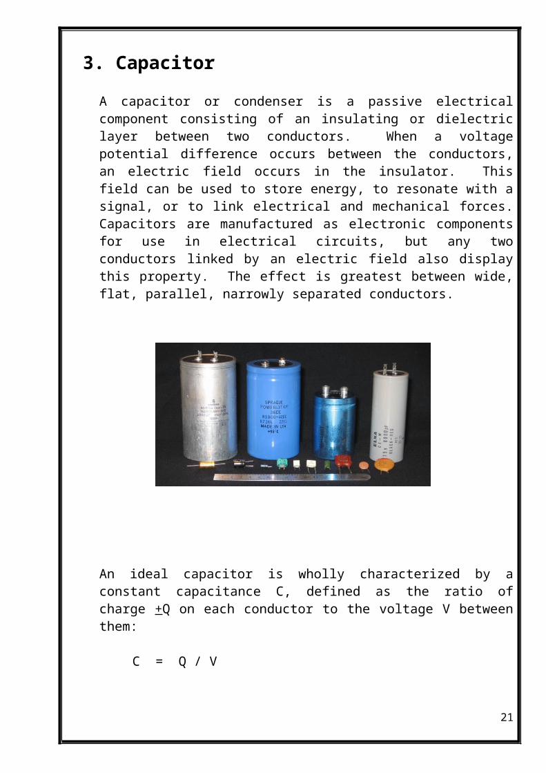
3. CapacitorA capacitor or condenser is a passive electrical component consisting of an insulating or dielectric layer between two conductors. When a voltage potential difference occurs between the conductors, an electric field occurs in the insulator. This field can be used to store energy, to resonate with a signal, or to link electrical and mechanical forces. Capacitors are manufactured as electronic components for use in electrical circuits, but any two conductors linked by an electric field also display this property. The effect is greatest between wide, flat, parallel, narrowly separated conductors.
An ideal capacitor is wholly characterized by a constant capacitance C, defined as the ratio of charge +Q on each conductor to the voltage V between them:
C = Q / V
The unit of capacitance is thus coulombs per volt, or farads. Higher capacitance indicates that more charge may be stored at a given energy level, or voltage. In actual capacitors, the insulator allows a small amount of current through, called leakage current, the conductors add an additional series resistance, and the insulator has an electric field strength limit resulting in a breakdown voltage.
15

4. Load ResistanceA resistor is a two-terminal electronic component that produces a voltage across its terminals that is proportional to the electric current through it in accordance with Ohm's law:
V = IR
*****************************
16

To observe the effects of changing the distance between screen and slit on the width
of central maxima in diffraction
17

1. Laser Source
2. Single Slit
3. Optical Bench
4. Screen
5. Scale & Pencil
18

DiffractionDiffraction of light is the phenomenon of bending of light around corners of an obstacle or aperture in the path of light. On account of this bending, light penetrates into the geometrical shadow of the obstacle. The light thus deviates from its linear path. Or in other words, Diffraction is normally taken to refer to various phenomena which occur when a wave encounters an obstacle. It is described as the apparent bending of waves around small obstacles and the spreading out of waves past small openings.
Diffraction of light through single slit(Graph)
19

Diffraction of light through single slit(Pattern Observed)
Single Slit Experiment
In this experiment, light coming from a monochromatic source, falls on a convex lens and a parallel beam of light is obtained. This parallel beam of light falls on the single slit. The rays of light bend through the edge and superimpose in the different phase on a different point in the screen.
As a result alternate dark and bright bands are obtained. These are called secondary bands i.e. secondary maxima or secondary minima. The central point has the maximum intensity and maximum width called Central Maxima.
Condition for Secondary MinimaPath difference = nλ (n=1, 2, 3…)
= asinθWhere,
a = width of slitTherefore,
It is because path difference between the waves coming from two paths of same wave front is λ/2 each. Hence, minima is obtained when path difference is a multiple of λ.
20
asinθ = nλ
Phase Difference
Thus
Condition for Secondary Maxima
Path Difference =
Phase Difference =
Thus,
Width of Central MinimaIt is the distance between two first secondary minima on both sides of central point.
For secondary minima : asinθ = n For n=1 asinθ = λ sinθ = λa ……( 1 )
For small angle : sinθ = θ = XnD ……( 2 )
21
Φ = 2nπ
asinθ = ( 2n+1 ) λ2
( 2n +1 )π = φ
Xn = (2n+1)λD2a
xn = nλDa

From 1 and 2:λa= XnD
Thus,
Width of Central Maxima
β = 2Xn = 2λDa
If lens are very close to the slit , then D ≈ f β = 2λf
a
Angular Width of Central Maxima
Sinθ ¿ λa=X nD
θ ¿ λa=X nD
Angular width = 2θ =2λa
=2 X nD
Factors affecting Width of Central Maxima
Considering the expression xn = λDa
Width of central maxima varies with the following parameters:
1. It varies directly with the wavelength of light.2. It varies directly with the distance between the screen and the slit.3. It is inversely proportional to the width of slit.
22
Xn = λDa

S.no Distance of screen( cm )
Width of central maxima( cm )
1.
2.
3.
The observations obtained show that width of central maxima increases with increase in the distance between the slit and the screen.
23

1. Wikipedia – The Free Encyclopedia
2. Physics NCERT Class XII
3. Textbook of Physics – Pradeep’s
4. Encarta Encyclopedia
5. Britannica Encyclopedia
24


![Project [Vishwa]](https://img.pdfslide.net/doc/110x75/577d369f1a28ab3a6b938b41/project-vishwa.jpg)