Embed Size (px)
Citation preview
DESIGN AND ANALYSIS OF FEEDBACK CONTROLLERS FOR A DC BUCK-BOOST CONVERTER Murdoch University: The Murdoch School of Engineering & Information Technology
Author: Jason Chan
Supervisors: Martina Calais & Simon Glenister

2 | P a g e
Abstract
In Murdoch University, students majoring in Electrical Power Engineering have the opportunity to
learn about the basics of power electronic systems. ENG349 Power Electronic Converters and
Systems is a unit where students are exposed to a range of industrial electronics. The power pole
board provided by the University of Minnesota is used for laboratory teaching on how DC converters
operate [1, 2]. This thesis topic gives an opportunity for Electrical Power students to further expand
their basic knowledge on power electronics.
Additionally, Instrumentation and Control System Engineering students will have a better
understanding of dynamic control systems, which are essential in designing and analysing feedback
control on DC converters. Industrial computer systems students are able to design and implement
external hardware to enhance power board components. Renewable Energy students will be
interested in how DC converters are applied to renewable energy systems. This thesis provides
project expansion for all types of electrical engineering majors taught at Murdoch University.
The main focus of this thesis is to design and analyse different feedback controllers for the converter
system. The literature review and steps into designing feedback controllers are adapted from Ned
Mohan’s approach in designing feedback controllers for DC converters [3]. The results presented are
based on the author’s knowledge learnt from Electrical Power and Instrumentation and Control
Systems Engineering.
Computer simulations from and are used for testing the feedback responses of
implementing different feedback compensators. The most difficult task in this thesis is to produce
accurate results from the power pole board, especially with the peak current controller circuit.
Although the simulated results are successful, it is hard to compare these to the experimental results
due to the ways of how the power board components are connected. This thesis will further explain
the process in exploring these feedback controllers.

3 | P a g e
Acknowledgements
I would like to acknowledge my supervisors, Dr Martina Calais and Simon Glenister, for providing
guidance and assistance in this project, and helping me to overcome difficulties I’ve experienced
during the year. I would also like to thank Iafeta Laava for technical support in the laboratory work,
which was essential in completing this thesis.
I would like to acknowledge the lecturers of Murdoch University for their valuable teaching time and
encouragements which have helped me to complete my degree. Finally, I would like to thank my
family and friends for their support.
23 November, 2014
Jason Chan

4 | P a g e
Contents Abstract ................................................................................................................................................... 2
Acknowledgements ................................................................................................................................. 3
Nomenclature ......................................................................................................................................... 6
Table of Figures ....................................................................................................................................... 9
List of Tables ......................................................................................................................................... 11
Chapter 1 - Introduction ....................................................................................................................... 12
1.1 Objectives and Aim ............................................................................................................... 12
1.2 Report Overview ......................................................................................................................... 12
Chapter 2 - Buck-boost converter review ............................................................................................. 13
2.1 DC converters .............................................................................................................................. 13
2.2 Buck-boost Converter Components ............................................................................................ 13
2.3 Buck-boost Operation in Continuous Conduction Mode ............................................................ 14
Chapter 3 - Control Aspects of DC Converters ...................................................................................... 17
3.1 Dynamic Average Model ............................................................................................................. 17
3.1.1 Ideal Transformer................................................................................................................. 19
3.2 Regulation with pulse width modulation .................................................................................... 21
Chapter 4 - Linearisation ....................................................................................................................... 22
4.1 Pulse Width Modulator Linearisation ......................................................................................... 22
4.2 Power Stage Linearisation ........................................................................................................... 23
4.3 Equivalent Circuit and Transfer Function of Converter .............................................................. 25
Chapter 5 - Bode Plots and Computer simulations ............................................................................... 26
5.1 Bode plots Review ....................................................................................................................... 27
5.2 Buck-boost Pole Zero Map .......................................................................................................... 29
5.3 PSpice Simulation on Power Stage
........................................................................................ 30
5.3.1 Open loop transient response ............................................................................................. 32
Chapter 6 - Feedback control compensator design .............................................................................. 34
6.1 Electronic control systems .......................................................................................................... 34
6.2 K Factor Method ......................................................................................................................... 35
6.2.1 Type 2 Amplifier ................................................................................................................... 35
6.2.2 Type 3 Amplifier ................................................................................................................... 36
6.3 Voltage mode control in Continuous Conduction Mode ............................................................ 37
6.3.1 Voltage Mode Controller Design .......................................................................................... 37
6.4 Peak current control in Continuous Conduction Mode .............................................................. 42
5 | P a g e
6.4.1 Peak current mode controller design .................................................................................. 43
Chapter 7 PSpice Feedback Controller Testing ..................................................................................... 46
7.1 Voltage Mode Control ............................................................................................................. 46
7.2 Peak Current Mode Control ........................................................................................................ 48
7.3 Performance Criteria Calculations .............................................................................................. 50
Chapter 8 – Power Pole Board .............................................................................................................. 50
8.1 Technical Specifications .............................................................................................................. 51
8.1.1 Signal Supply ........................................................................................................................ 51
8.1.2 Load ...................................................................................................................................... 51
8.1.3 Frequency Analysis ............................................................................................................... 52
8.1.4 Controller Selection Jumpers ............................................................................................... 52
8.1.5 Current Measurement ......................................................................................................... 52
8.1.6 PWM Signal Generation ....................................................................................................... 52
8.2 Open Loop Operation in CCM ..................................................................................................... 53
8.3 Finding the Transfer Function of the Buck-boost Power Board ................................................. 55
8.4 Closed loop Operation (Peak current control mode) ................................................................. 55
Chapter 9 – Power Pole Board Testing ................................................................................................. 56
9.1 Buck-boost Transfer Function Findings ....................................................................................... 57
9.2 Peak Current Mode Control ........................................................................................................ 58
Chapter 10 – Conclusion ....................................................................................................................... 61
Chapter 10.1 Future Work ................................................................................................................ 62
References ............................................................................................................................................ 63
Appendix A - Power pole board ............................................................................................................ 65
A-1 Power board part locations ........................................................................................................ 65
A-2 Type 2 Amplifier Breadboard and PWM Connections ............................................................... 68
Appendix B – MATLAB Code for Buck-boost Analysis and Controller Design ....................................... 69
B-1 Buck-boost Type 3 Amplifier Transfer Function ......................................................................... 69
B-2 Buck-boost Type 2 Amplifier Transfer Function ......................................................................... 70

6 | P a g e
Nomenclature
–
–
–
–
–
–
–
–
–
–
–

7 | P a g e
–
–
–

8 | P a g e
9 | P a g e
Table of Figures
Figure 1 DC Converter Block Diagram ................................................................................................... 13
Figure 2 Buck-boost Converter ............................................................................................................. 14
Figure 3 n channel MOSFET .................................................................................................................. 14
Figure 4 Buck-boost Conduction MOSFET states and Waveforms ....................................................... 15
Figure 5 Dynamic Average Model Configurations ................................................................................ 18
Figure 6 Buck-boost Dynamic Average Model ...................................................................................... 19
Figure 7 DC Converter Equivalent Model ............................................................................................. 20
Figure 8 DC Ideal Transformer Model ................................................................................................... 20
Figure 9 Pulse Width Modulation Output Regulation .......................................................................... 21
Figure 10 PWM Amplifier and Comparator Block Diagram .................................................................. 21
Figure 11 PWM UC3824 Linearisation .................................................................................................. 22
Figure 12 Switching Power Pole Linearisation ...................................................................................... 24
Figure 13 Linearised Buck-boost Model ............................................................................................... 25
Figure 14 DC Converter Equivalent Circuit ........................................................................................... 26
Figure 15 Magnitude Bode plot linear relationships ............................................................................ 27
Figure 16 Buck-boost Transfer Function P-Z Map Code ....................................................................... 29
Figure 17 Poles and Zeros Locations for Buck-boost Transfer Function ............................................... 29
Figure 18 Pspice Drawing of Buck-boost Dynamic Model .................................................................... 30
Figure 19 PSpice frequency response of buck-boost power stage
.................................................. 31
Figure 20 Buck-boost Open Loop Dynamic Circuit ............................................................................... 32
Figure 21 Buck-boost Open Loop Transient Response ......................................................................... 33
Figure 22 Type 2 Amplifier (a) and Bode Plot (b) .................................................................................. 35
Figure 23 Type 3 Amplifier (a) and Bode Plot (b) .................................................................................. 36
Figure 24 Voltage mode controller block diagram ............................................................................... 37
Figure 25 MATLAB Bode Plot of Type 3 Amplifier Transfer Function ................................................... 38
Figure 26 Peak current mode controller block diagram ....................................................................... 42
Figure 27 Peak Current Control with Slope Compensation .................................................................. 42
Figure 28 PSpice Bode Plot for Power Stage
..................................................................................... 43
Figure 29 MATLAB Bode Plot of Type 2 Amplifier Transfer Function ................................................... 43
Figure 30 Pspice Buck-boost Voltage Mode Controller Circuit ............................................................. 46
Figure 31 Voltage Mode Control Transient Response .......................................................................... 47
Figure 32 Pspice Buck-boost Peak Current Controller Circuit............................................................... 48
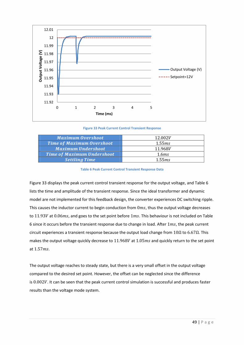
Figure 33 Peak Current Control Transient Response ............................................................................ 49
Figure 34 Power Pole Board Diagram ................................................................................................... 51
Figure 35 Buck-boost Power Board Configuration Diagram ................................................................. 54
Figure 36 Power Pole Board Equipment Set Up ................................................................................... 56
Figure 37 Buck-boost Power Pole Board Magnitude Log Scale Plot ..................................................... 57
Figure 38 Buck-boost Power Pole Board Phase Plot ............................................................................. 58
Figure 39 Type 2 Amplifier Breadboard Connections ........................................................................... 58
Figure 40 Unstable PWM(purple) and Inductor Current(blue) Oscilloscope Waveforms (Output
Voltage=10.28V).................................................................................................................................... 59

10 | P a g e
Figure 41 Slope Compensation Jumper ................................................................................................ 60
Figure 42 PWM(purple) and Inductor Current(blue) Oscilloscope Waveforms - with slope
compensation ....................................................................................................................................... 61
Figure 43 Power Pole Board Component Locations ............................................................................. 65
Figure 44 Power pole Board Circuit Drawing with Peak Current Control Board .................................. 68

11 | P a g e
List of Tables Table 1 Buck-boost Converter Parameter Parts and Values ................................................................. 26
Table 2 Open loop transient response data.......................................................................................... 33
Table 3 Type 3 Amplifier Parameters for Voltage Mode Control Implementation .............................. 41
Table 4 Type 2 Amplifier Parameters for Peak Current Control Implementation ................................ 45
Table 5 Voltage Mode Control Transient Response Data ..................................................................... 47
Table 6 Peak Current Control Transient Response Data ....................................................................... 49
Table 7 Control System Performance Criteria Values ........................................................................... 50
Table 8 Type 2 Amplifier Breadboard Components .............................................................................. 59
Table 9 Slope Compensation Jumper Values ........................................................................................ 61
Table 10 Component locations on Power pole Board .......................................................................... 66
Table 11 Test points on the Power pole Board ..................................................................................... 67

12 | P a g e
Chapter 1 - Introduction
This chapter will introduce the overall structure of this thesis report. This includes the objectives in
completing different tasks and how to analyse the final results.
1.1 Objectives and Aim
The aim of this project is to develop and analyse different feedback concepts for the buck-boost
converter. This project represents an expansion of Luke Morrison’s thesis, including the voltage
mode controller for the buck converter [4]. The literature background is reviewed for the buck-boost
converter, as well as the steps in completing feedback controllers for the closed loop system.
Computer simulations are used to model the buck-boost model and the feedback controllers. A
simple comparison is made to determine which feedback concept is more effective. The parameter
values are calculated from coding, and implemented from an external source. The final
task of the project is to implement a peak current compensator onto the power pole board, and
analyse the effects it has on the hardware.
1.2 Report Overview
The report begins in Chapter 2 with a literature review on the buck-boost converter in continuous
conduction mode. Chapter 3 explains the DC control aspects which can affect the final feedback
responses. Chapter 4 covers linearisation techniques required for transfer functions of the DC
converter and feedback controllers. Chapter 5 shows a description of Bode plots for analysing
transfer functions. Simulated results of the buck-boost converter are included in the chapter.
Chapter 6 covers the literature review of designing feedback controllers for the buck-boost
converter. This chapter also includes the final calculations of the feedback controller parts. The
feedback controller results produced from schematics are in Chapter 7. Chapter 8 include
descriptions of the Power Board components and how to obtain laboratory results. Chapter 9
includes the results for the buck-boost converter configured on the board, as well as the peak
current control compensator testing. Finally, Chapter 10 concludes this thesis report with
recommendations on further improvements and project expansion in the future.
13 | P a g e
Chapter 2 - Buck-boost converter review
This chapter provides the theoretical background on the buck-boost converter selected for project
analysis.
2.1 DC converters
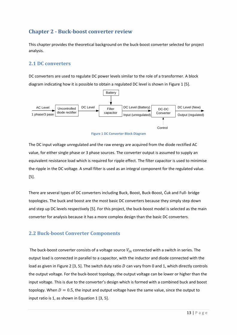
DC converters are used to regulate DC power levels similar to the role of a transformer. A block
diagram indicating how it is possible to obtain a regulated DC level is shown in Figure 1 [5].
DC Level (Battery)
Input (unregulated)
DC Level (New)
Output (regulated)
Control
DC-DC
Converter
Filter
capacitor
Battery
Uncontrolled
diode rectifier
AC Level
1 phase/3 pase
DC Level
Figure 1 DC Converter Block Diagram
The DC input voltage unregulated and the raw energy are acquired from the diode rectified AC
value, for either single phase or 3 phase sources. The converter output is assumed to supply an
equivalent resistance load which is required for ripple effect. The filter capacitor is used to minimise
the ripple in the DC voltage. A small filter is used as an integral component for the regulated value.
[5].
There are several types of DC converters including Buck, Boost, Buck-Boost, Ćuk and Full- bridge
topologies. The buck and boost are the most basic DC converters because they simply step down
and step up DC levels respectively [5]. For this project, the buck-boost model is selected as the main
converter for analysis because it has a more complex design than the basic DC converters.
2.2 Buck-boost Converter Components
The buck-boost converter consists of a voltage source connected with a switch in series. The
output load is connected in parallel to a capacitor, with the inductor and diode connected with the
load as given in Figure 2 [3, 5]. The switch duty ratio can vary from 0 and 1, which directly controls
the output voltage. For the buck-boost topology, the output voltage can be lower or higher than the
input voltage. This is due to the converter’s design which is formed with a combined buck and boost
topology. When , the input and output voltage have the same value, since the output to
input ratio is 1, as shown in Equation 1 [3, 5].
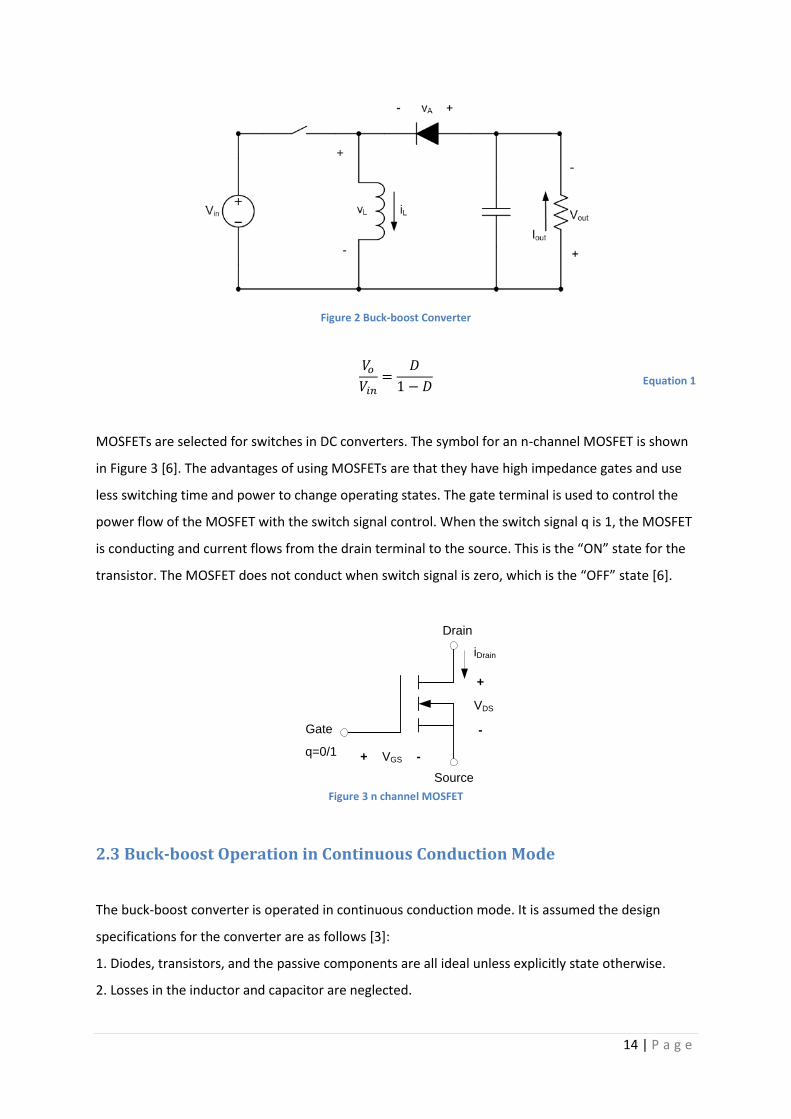
14 | P a g e
Figure 2 Buck-boost Converter
Equation 1
MOSFETs are selected for switches in DC converters. The symbol for an n-channel MOSFET is shown
in Figure 3 [6]. The advantages of using MOSFETs are that they have high impedance gates and use
less switching time and power to change operating states. The gate terminal is used to control the
power flow of the MOSFET with the switch signal control. When the switch signal q is 1, the MOSFET
is conducting and current flows from the drain terminal to the source. This is the “ON” state for the
transistor. The MOSFET does not conduct when switch signal is zero, which is the “OFF” state [6].
Gate
Drain
Source
iDrain
VGS
VDS
+ -
+
-
q=0/1
Figure 3 n channel MOSFET
2.3 Buck-boost Operation in Continuous Conduction Mode
The buck-boost converter is operated in continuous conduction mode. It is assumed the design
specifications for the converter are as follows [3]:
1. Diodes, transistors, and the passive components are all ideal unless explicitly state otherwise.
2. Losses in the inductor and capacitor are neglected.
15 | P a g e
3. Switching frequency and duty ratio need to be constant over each cycle.
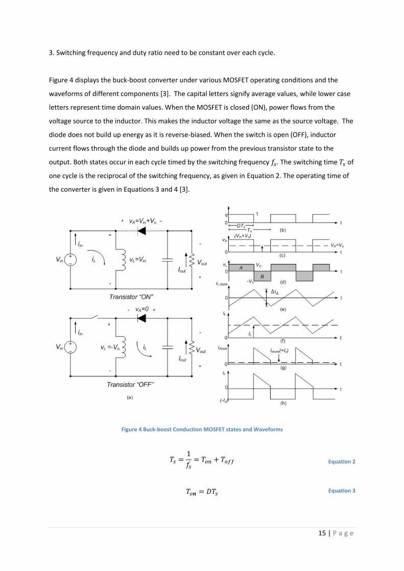
Figure 4 displays the buck-boost converter under various MOSFET operating conditions and the
waveforms of different components [3]. The capital letters signify average values, while lower case
letters represent time domain values. When the MOSFET is closed (ON), power flows from the
voltage source to the inductor. This makes the inductor voltage the same as the source voltage. The
diode does not build up energy as it is reverse-biased. When the switch is open (OFF), inductor
current flows through the diode and builds up power from the previous transistor state to the
output. Both states occur in each cycle timed by the switching frequency . The switching time of
one cycle is the reciprocal of the switching frequency, as given in Equation 2. The operating time of
the converter is given in Equations 3 and 4 [3].
Figure 4 Buck-boost Conduction MOSFET states and Waveforms
Equation 2
Equation 3

16 | P a g e
During the ON state, the diode voltage equals the sum of the input and output voltages as given
in Equation 5. The average diode voltage has the same value as the output voltage for DC steady
state conditions due to no power being dissipated in the inductor. When the MOSFET is in the OFF
state, the diode voltage drops to zero from the ON state. Figure 4(c) displays the diode voltage
waveform [3].
Equation 5
Figure 4(d) displays the inductor voltage waveform which changes instantaneously between the ON
and OFF state [3]. During the ON state, the power flow causes the inductor to have the same voltage
as the input supply, as given in Equation 6. During the OFF state, the inductor voltage is equal to the
negative polarity of the output voltage, as given in Equation 7. The negative polarity is cause by the
fixed direction of the current flowing through the capacitor and output load [7]. The voltages for the
diode and inductor remains constant during each MOSFET state, whereas the currents have time
based linear relationships [3].
Equation 6
Equation 7
By applying the Kirchhoff’s current law in the converter, the inductor current is obtained from the
addition of the input and output currents as given in Equation 8. The output current is obtained from
the ohm’s law relationship between the output voltage and load, which can be substituted into the
inductor current equation with Equation 1. In DC steady state, the average capacitor current is zero
[3].
Equation 8
Over time, the inductor current is obtained from the sum of the average inductor current and the
time domain ripple inductor current as given in Equation 9. The inductor current has average value
Equation 4
17 | P a g e
of zero and experiences ripple through each state (rises when is positive and drops when is
negative). The peak-peak ripple value can be calculated from Area A or B as given in Equation 10 [3].
Equation 9
As displayed in Figure 4(d), area A and B has must possess the same scale and opposing polarity,
which represent volt-second areas. This is because the average inductor current is zero. It is possible
to obtain the ratio for input/output voltage values from the or since the average value of the
inductor voltage is zero [3].
Equation 10
It is necessary for the capacitor to possess a very large value in order to achieve a constant output
voltage. The capacitor has lower impedance in the ripple inductor current than the load resistance,
therefore it is presumed the ripple diode current passes through the capacitor, as shown in Equation
11 [3]. When forming the equivalent circuit, the capacitor will be connected with an equivalent
series resistance (ESR) for dispersing heat power [8].
Equation 11
The buck-boost configuration on the power pole board should display these waveforms to confirm
the components are not malfunctioning.
Chapter 3 - Control Aspects of DC Converters This chapter covers control aspects which can affect the feedback analysis of DC converters. This
includes the dynamic average model required for DC converters, DC ideal transformer, and the pulse
width modulation (PWM) implemented on the converter simulations and hardware.
3.1 Dynamic Average Model
Dynamic average models are preferable for analysing feedback control in DC converters. The
dynamic conditions are determined by the change in output load and input voltage. It is assumed
18 | P a g e
the operating time is relatively slow and frequencies of average values are lower than the switching
frequency [3].
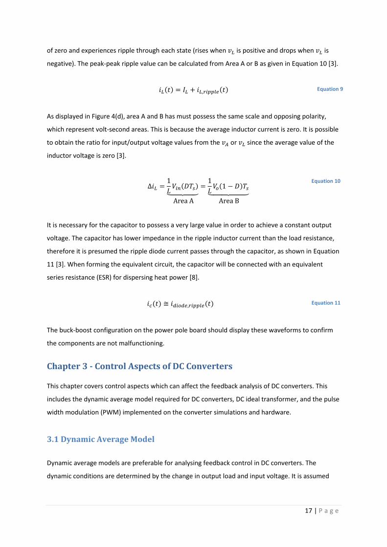
Figure 5 Dynamic Average Model Configurations
Figure 5 displays the configuration in implementing a dynamic average model into DC converters.
The figures have voltages and currents with the following subscript meanings: voltage port (‘ ’) and
current-port (‘ ’). The voltage port refers to the input terminals, while the current port refers to the
output terminals [3].
Figure 5(a) is the MOSFET switching power pole connected with the diode. The switching signal q is
based on the ratio between the control voltage and ramp voltage , which are further explained
in Chapter 3.2. The switching states make it difficult to perform analysis with any change of input
voltage or output load.
Figure 5((b) displays an ideal transformer for the DC steady state average model. This model is
suitable for performing transient analysis on the converter. The DC steady state values are
represented by capital letters: and , while lower case represents the full dynamic time varying
quantities [3].
The voltage-port voltage should not have a negative polarity as the duty ratio has to be within the
range 0 to 1. Assuming the switching power pole is functional for DC and AC applications, the ideal
transformer is theoretical and recommended for mathematical problems. The disadvantage of using
a real transformer is that it cannot perform the same behaviour. This is signified by the parallel
straight and curved line below the transformer. There is no electrical isolation between the voltage-
19 | P a g e
port and the current-port, as signified by the connection at the bottom of the windings of the
transformer in Figure 5(b) [3].
The MOSFET and diode devices are replaced by the ideal transformer model, which completes the
dynamic average model in Figure 5(c). Equations for time domain average values are formed from
the model, as given in Equations 12 and 13. The DC average values are represented by a bar over the
lowercase letters [3].
Equation 12
Equation 13
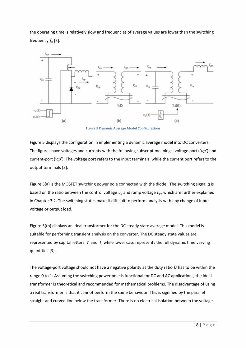
Figure 6 Buck-boost Dynamic Average Model
Figure 6 displays the conversion from the buck-boost MOSFET/switching pole circuit to the dynamic
average model, which is applied in simulations and tested for output transient response. The ideal
transformer replaces the MOSFET/diode switching pole in the buck-boost configuration which
eliminates the switching conditions for dynamic analysis [3].
3.1.1 Ideal Transformer
The ideal transformer is the main component of the dynamic average model. It is responsible for
cancelling the DC switching ripple, as required for DC performance analysis [9]. This makes the
circuit a switching electronic converter rather than a simple transformer [10]. Figure 7 displays the
DC converter equivalent model which has dependent sources for manipulating the input current and
20 | P a g e
output voltage. The circuit relationships are distinguished in Equations 14 and 15, which applies for
all types of converters [9].
+
-
+
-
+
-
Input Terminal Output Terminal
Figure 7 DC Converter Equivalent Model
Equation 14
Equation 15
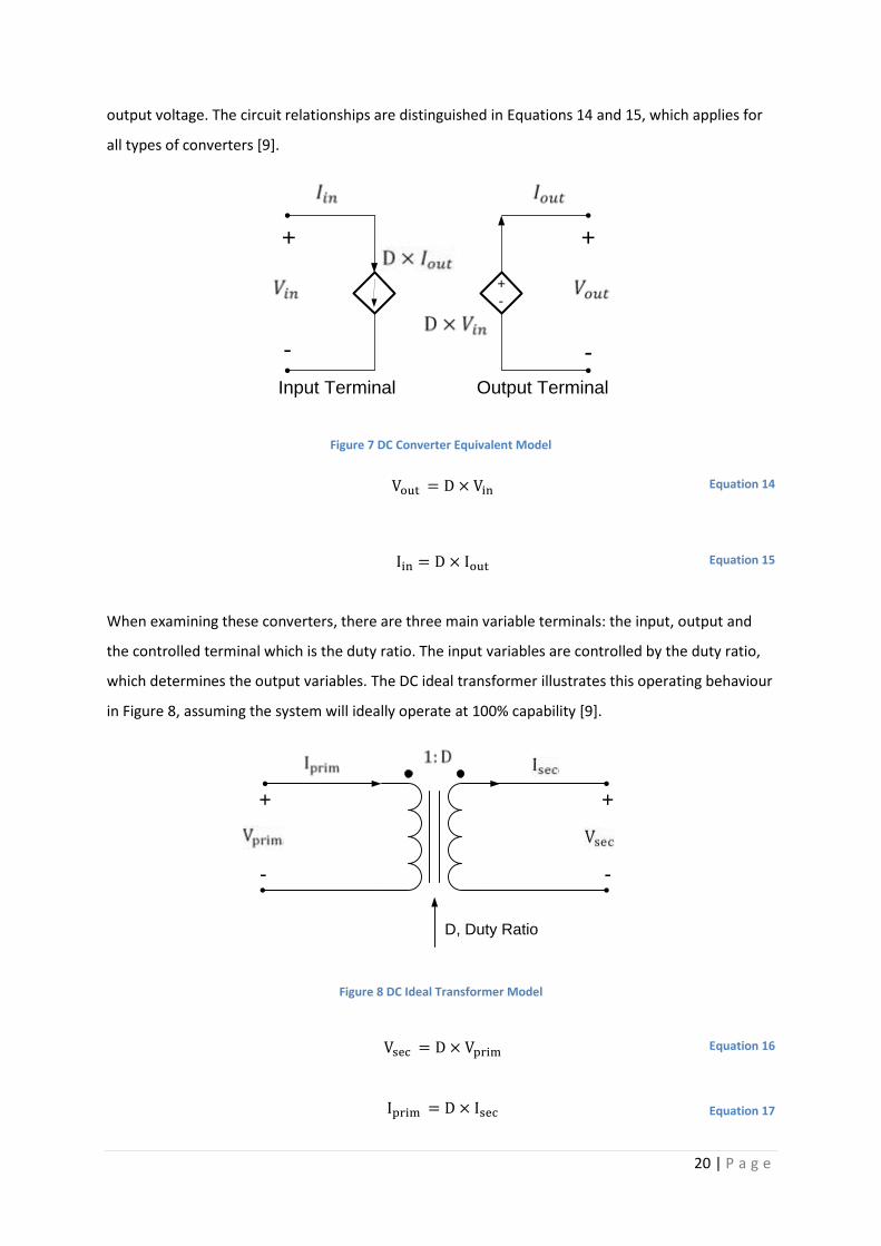
When examining these converters, there are three main variable terminals: the input, output and
the controlled terminal which is the duty ratio. The input variables are controlled by the duty ratio,
which determines the output variables. The DC ideal transformer illustrates this operating behaviour
in Figure 8, assuming the system will ideally operate at 100% capability [9].
+
-
+
-
D, Duty Ratio
Figure 8 DC Ideal Transformer Model
Equation 16
Equation 17

21 | P a g e
The advantage of using an ideal transformer is that it does not disturb the energy going through the
model [10]. Therefore, the input and output terminals should experience the same amount of power
as shown in Equations 18 and 19.
Equation 18
Equation 19
When simulating the buck-boost converter with the ideal transformer, the input and output voltages
should be based on the relationship that is given by equations in Chapter 2.2.
3.2 Regulation with pulse width modulation
Pulse width modulation (PWM) is used for manipulating DC output at a constant switching
frequency. It modulates the pulse width to control the average value of the switching cycle output.
The duty ratio is directly related to the pulse width and the output voltages to match their desired
values and range. It will react to any changes in the input voltage and output load disturbances [3].
Figure 9 Pulse Width Modulation Output Regulation
Figure 10 PWM Amplifier and Comparator Block Diagram
22 | P a g e
Figure 9 displays a block diagram and waveforms of an output regulated DC converter for this case
[3]. In the PWM controller, the output voltage is measured and contrasted with its reference value.
An amplifier is used to measure the error between the two values, as shown in Figure 10 [5]. The
output value of the amplifier is the control voltage . The comparator is used for comparing the
control voltage with the ramp voltage to determine the switch control signal q. When the ramp
voltage exceeds the control voltage, the MOSFET switch signal will go to zero (OFF state). The ramp
peak is the final ramp value at the end of each MOSFET cycle [3].
Chapter 4 - Linearisation
This chapter covers linearisation in order to obtain transfer functions required for the closed loop
converter system. The purpose of linearisation is to take in account all DC components operating
around dc steady state points and obtain the small signal model for the DC equivalent circuit.
4.1 Pulse Width Modulator Linearisation
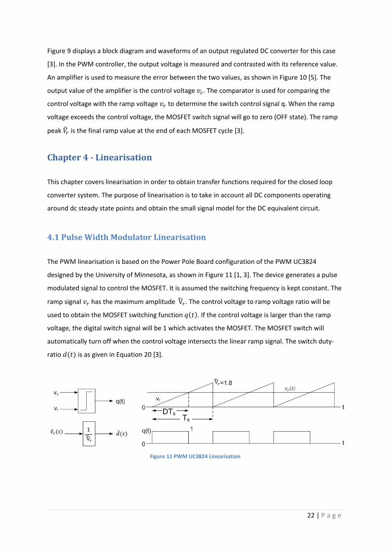
The PWM linearisation is based on the Power Pole Board configuration of the PWM UC3824
designed by the University of Minnesota, as shown in Figure 11 [1, 3]. The device generates a pulse
modulated signal to control the MOSFET. It is assumed the switching frequency is kept constant. The
ramp signal has the maximum amplitude . The control voltage to ramp voltage ratio will be
used to obtain the MOSFET switching function . If the control voltage is larger than the ramp
voltage, the digital switch signal will be 1 which activates the MOSFET. The MOSFET switch will
automatically turn off when the control voltage intersects the linear ramp signal. The switch duty-
ratio is as given in Equation 20 [3].
Figure 11 PWM UC3824 Linearisation

23 | P a g e
Equation 20
The time domain control voltage is based on the addition of small signal disturbance and the DC
steady state operating point, as given in Equation 21 [3].
Equation 21
Using the relationships in Equations 20 and 21, it is possible to substitute these variables into the
power stage duty cycle equation, which makes up Equation 22 [3].
Equation 22
Equation 22 is easily separated into the small signal variable for obtaining the PWM unit transfer
function. The transfer function is the small signal ratio of the duty ratio to the control voltage, as
given in Equation 23. This proves the PWM has a pure gain value as the final equation is a reciprocal
of the ramp to peak amplitude [3].
Equation 23
The Unitrode/Texas Instruments has provided a datasheet listing the characteristics of different high
speed PWM controllers. The UC3824 ramp valley to peak is [11], which is substituted into
Equation 23 to calculate the PWM gain, as given in Equation 24 [3].
Equation 24
This completes the linearisation for the PWM controller configured on the Power Pole board.
4.2 Power Stage Linearisation
Before creating feedback compensators for the DC converter, linearisation must be applied to the
buck-boost power stage. It is assumed a small signal disturbance will occur on the DC switching
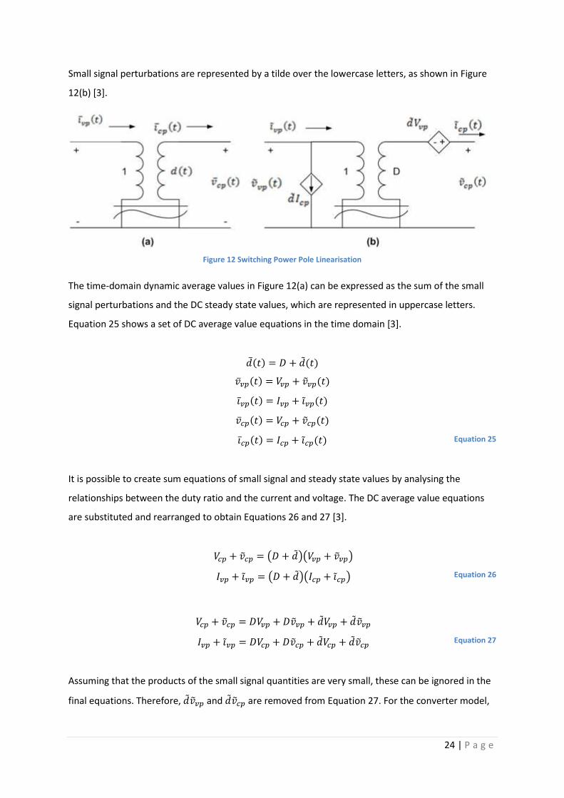
power pole. The linearised average model of the switching power pole is shown in Figure 12(a).
24 | P a g e
Small signal perturbations are represented by a tilde over the lowercase letters, as shown in Figure
12(b) [3].
Figure 12 Switching Power Pole Linearisation
The time-domain dynamic average values in Figure 12(a) can be expressed as the sum of the small
signal perturbations and the DC steady state values, which are represented in uppercase letters.
Equation 25 shows a set of DC average value equations in the time domain [3].
Equation 25
It is possible to create sum equations of small signal and steady state values by analysing the
relationships between the duty ratio and the current and voltage. The DC average value equations
are substituted and rearranged to obtain Equations 26 and 27 [3].
Equation 26
Equation 27
Assuming that the products of the small signal quantities are very small, these can be ignored in the
final equations. Therefore, and are removed from Equation 27. For the converter model,
25 | P a g e
Equation 26 is decomposed to form equations for the DC steady state variables (Equation 28) and
small signal linear representation given by steady state conditions (Equation 29) [3].
Equation 28
Equation 29
The small signal equations can be used to find the converter’s power stage transfer function, which
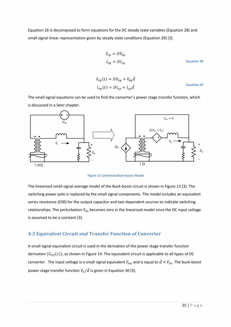
is discussed in a later chapter.
Figure 13 Linearised Buck-boost Model
The linearised small signal average model of the Buck-boost circuit is shown in Figure 13 [3]. The
switching power pole is replaced by the small signal components. The model includes an equivalent
series resistance (ESR) for the output capacitor and two dependent sources to indicate switching
relationships. The perturbation becomes zero in the linearised model since the DC input voltage
is assumed to be a constant [3].
4.3 Equivalent Circuit and Transfer Function of Converter
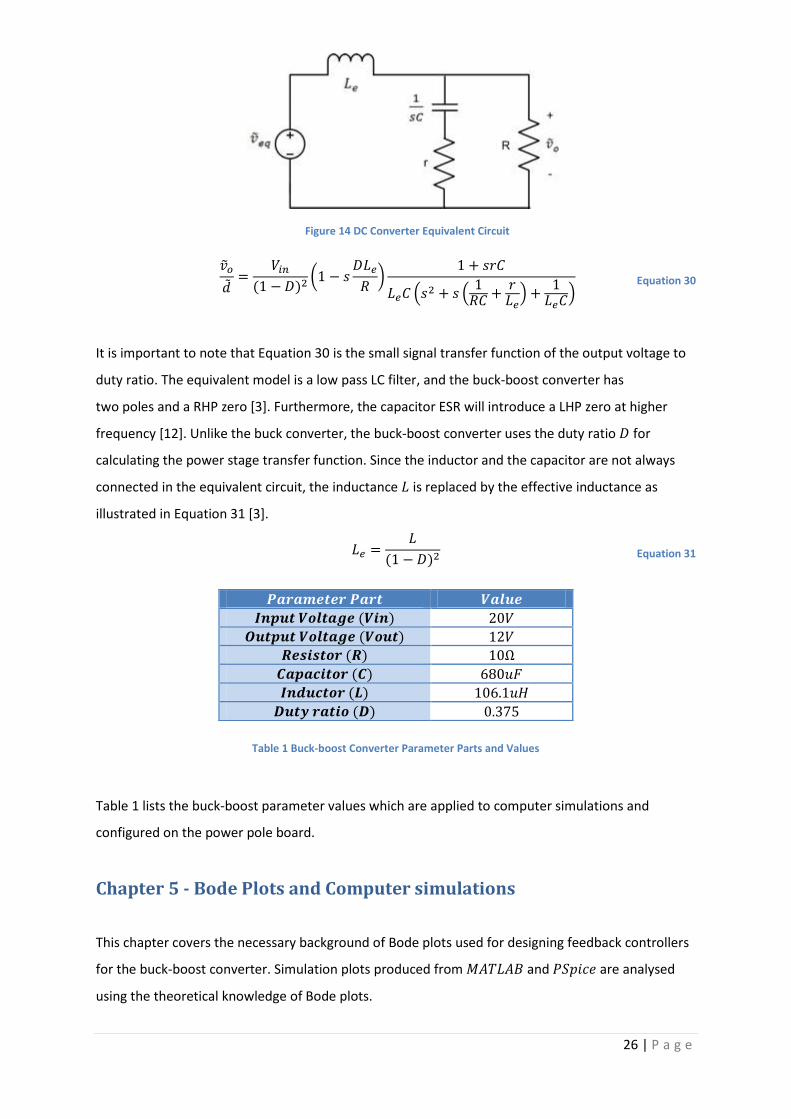
A small signal equivalent circuit is used in the derivation of the power stage transfer function
derivation , as shown in Figure 14. The equivalent circuit is applicable to all types of DC
converter . The input voltage is a small signal equivalent and is equal to . The buck-boost
power stage transfer function is given in Equation 30 [3].
26 | P a g e
Equation 30
It is important to note that Equation 30 is the small signal transfer function of the output voltage to
duty ratio. The equivalent model is a low pass LC filter, and the buck-boost converter has
two poles and a RHP zero [3]. Furthermore, the capacitor ESR will introduce a LHP zero at higher
frequency [12]. Unlike the buck converter, the buck-boost converter uses the duty ratio for
calculating the power stage transfer function. Since the inductor and the capacitor are not always
connected in the equivalent circuit, the inductance is replaced by the effective inductance as
illustrated in Equation 31 [3].
Equation 31
Table 1 Buck-boost Converter Parameter Parts and Values
Table 1 lists the buck-boost parameter values which are applied to computer simulations and
configured on the power pole board.
Chapter 5 - Bode Plots and Computer simulations
This chapter covers the necessary background of Bode plots used for designing feedback controllers
for the buck-boost converter. Simulation plots produced from and are analysed
using the theoretical knowledge of Bode plots.
Figure 14 DC Converter Equivalent Circuit
27 | P a g e
5.1 Bode plots Review
Bode plots can be used to illustrate the frequency response of DC converters as magnitude and
plots. The magnitude is in decibels, and phase is in degrees. Before conducting simulation runs on
the system, it is useful to review how these plots should appear based on the transfer function [9].
The magnitude in decibels is defined in Equation 32, where M can be dimensionless.
Equation 32
The bode plot defines a crossover frequency , where the magnitude is 0 or 1 dB. Given the
magnitude is a dimensionless quantity with and which are constants (Equation 33),
Equation 32 is rearranged to Equation 34 [9].
Equation 33
Equation 34
Figure 15 Magnitude Bode plot linear relationships
Figure 15 signifies how different values of affects the Bode plot magnitude over several decades in
frequencies. As indicated in Equation 34, an increase of is due to a decade increase in
frequency. Therefore, the gradient of the magnitude is [9].

28 | P a g e
By using Bode plots to display the frequency response of various transfer functions, it is possible to
analyse how a single pole and single zero affect the magnitude and phase individually. For
,
the value of is -1 which makes the magnitude gradient . This is the asymptote for
a single real pole transfer function. The magnitude consists of a low frequency asymptote of
and decreases by approximately after intersection with crossover frequency.
The phase is for a low frequency asymptote, and at crossover frequency. The phase
gradient is until the higher frequency asymptote phase is . [9].
For
, the value of is 1 which makes the magnitude gradient . This is the
asymptote for a single real zero transfer function. The magnitude consists of a low frequency
asymptote of and increases by approximately after intersection with
crossover frequency. The phase is for the low frequency asymptote, and at crossover
frequency. After the crossover frequency, the phase angle decreases each decade until it reaches
at larger frequency. Therefore, the phase gradient is [9].
For
, the value of is -2 which makes the magnitude gradient . This is the
asymptote for a two pole transfer function. The magnitude consists of low frequency asymptote of
and decreases by after intersection with crossover frequency. The phase is
for low frequency asymptote, and at crossover frequency. After the crossover frequency,
the phase angle decreases each decade until it reaches at larger frequencies. At the
crossover frequency (Equation 35), there maybe a peak which is determined by the quality factor .
It measures the amount of dissipation in the system, which can be calculated using Equation 36.
When increasing the value of , it makes the phase change sharper between the and
asymptote [9].
Equation 35
Equation 36
29 | P a g e
5.2 Buck-boost Pole Zero Map
It is easily possible to generate a bode plot the buck-boost transfer function using .
Additionally, the syntax ‘pzmap’ allows the user to map the pole and zero locations of transfer
functions [13]. Using the equations and parameters introduced from Chapter 4.3, the equivalent
code script has created and is shown in Figure 16.
Figure 16 Buck-boost Transfer Function P-Z Map Code
Figure 17 Poles and Zeros Locations for Buck-boost Transfer Function

30 | P a g e
Figure 17 shows the locations of the poles and zeros of the configured buck-boost converter. The
two complex poles are located at frequency which will result in the buck-boost magnitude
decreasing at and the phase shift lags by 180° [9]. Both poles are lying near the
imaginary axis, but are located on different real axis points. This signifies the buck-boost open loop
transient response will be oscillatory and takes a significant amount of time to reach steady state
[14].
The capacitor ESR creates the LHP zero at . The RHP zero is introduced from the buck-boost
circuit at which makes the magnitude to fall at , and introduce an additional
phase lag [9]. The contact between the two zeros will neglect the RHP zero effects on higher
frequencies [15]. Despite this condition, it is likely that the RHP zero will still cause problems when
designing feedback compensators to control the buck-boost system [16].
5.3 PSpice Simulation on Power Stage
Schematic is a very effective simulation package for drawing and analysing electrical circuits.
The University of Minnesota have created a schematic file of circuit components for designing the
DC converters [2, 3]. The buck-boost dynamic model is adapted from Ned Mohan’s
research on designing the peak current compensator, as shown in Figure 18 [3]. Through this
simulation package, it is possible to obtain the frequency response for the power stage transfer
function
[2].
Figure 18 Pspice Drawing of Buck-boost Dynamic Model
31 | P a g e
The buck-boost dynamic model makes use of an ideal transformer, which includes dependent
sources for the voltage and current. The duty ratio is determined by the DC voltage source V2. An
AC voltage source is connected in series for small signal perturbations. It has an amplitude of 1V
because the model is linearised before AC analysis. The parameter values are entered into the
program and located on the side of the circuit in Figure 18 [3].
Figure 19 PSpice frequency response of buck-boost power stage
Figure 19 shows the frequency response for the buck-boost power stage transfer function (
). The
plot shows the low frequency asymptote has a magnitude of and phase angle . Since the
power stage has two poles in the transfer function, the power exhibits a resonant peak of at
frequency , where the phase drops to . According to Robert W. Erikson’s explanation
on two pole transfer function, the quality factor on the Bode plot is the difference between the
peak magnitude and the low frequency asymptote, as calculated in Equation 37 [9]. is also
calculated with the buck-boost component values in Equation 38. The calculated magnitude gives
results which are quite similar to the Bode plot.
Equation 37
Equation 38
32 | P a g e
For moderate frequency ranges, the magnitude gradient is calculated using the values from
and . This will ensure the gradient is expressed in , since one decade is a 10
fold increase in frequency [9]. The magnitude gradient is calculated in Equation 39, which the value
is very similar to the expected result.
Equation 39
For designing a feedback controller, the design frequency has to be as large as possible for a quick
closed loop response. The value should exceed the resonant frequency , as calculated in Equation
40.
The phase angle should not exceed before the magnitude and phase angle intersects the
crossover frequency [3]. Furthermore, the instability effect caused by the RHP zero can be neglected
with larger frequencies [16].
5.3.1 Open loop transient response
Figure 20 Buck-boost Open Loop Dynamic Circuit
Equation 40
33 | P a g e
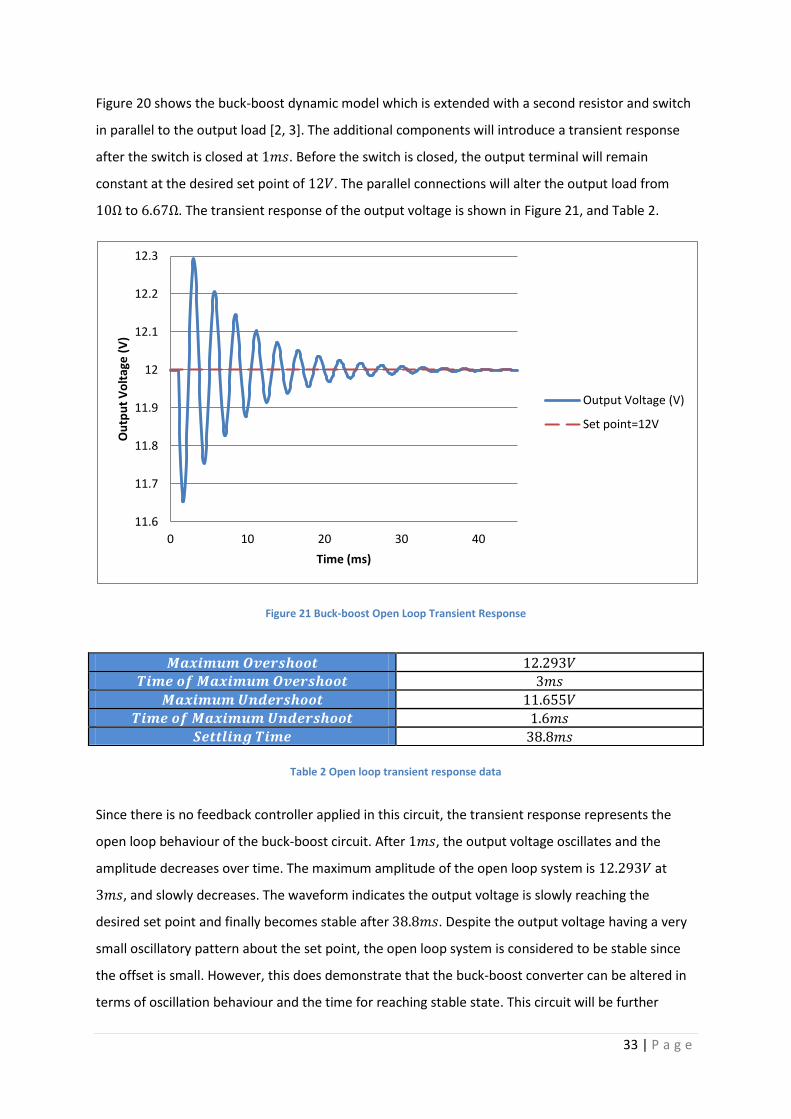
Figure 20 shows the buck-boost dynamic model which is extended with a second resistor and switch
in parallel to the output load [2, 3]. The additional components will introduce a transient response
after the switch is closed at . Before the switch is closed, the output terminal will remain
constant at the desired set point of . The parallel connections will alter the output load from
to . The transient response of the output voltage is shown in Figure 21, and Table 2.
Figure 21 Buck-boost Open Loop Transient Response
Table 2 Open loop transient response data
Since there is no feedback controller applied in this circuit, the transient response represents the
open loop behaviour of the buck-boost circuit. After , the output voltage oscillates and the
amplitude decreases over time. The maximum amplitude of the open loop system is at
, and slowly decreases. The waveform indicates the output voltage is slowly reaching the
desired set point and finally becomes stable after . Despite the output voltage having a very
small oscillatory pattern about the set point, the open loop system is considered to be stable since
the offset is small. However, this does demonstrate that the buck-boost converter can be altered in
terms of oscillation behaviour and the time for reaching stable state. This circuit will be further
11.6
11.7
11.8
11.9
12
12.1
12.2
12.3
0 10 20 30 40
Ou
tpu
t V
olt
age
(V
)
Time (ms)
Output Voltage (V)
Set point=12V

34 | P a g e
expanded and analysed after a description of designing different feedback controllers in the next
chapter.
Chapter 6 - Feedback control compensator design
This chapter covers the concept of feedback control systems, and techniques in designing different
feedback controllers for the buck-boost converter. There are two feedback systems applied in this
thesis: voltage mode control and peak current control. This chapter includes the steps in designing
and implementing the desired feedback compensators. The purpose of designing feedback
controllers is to apply and test closed loop operation in the Power Pole board and computer
simulations.
6.1 Electronic control systems
The buck-boost converter is a form of electronic control system, since it consists of a system formed
by electrical components [17]. These components create the DC input and output relationships, as
explained in earlier chapters. In terms of control systems, there are two different types which will be
used in this thesis: open loop and closed loop.
The open loop system does not have any feedback relationships between the output and input
terminals, creating an unregulated process. This makes it difficult to control the amount of
oscillations and time to reach the set point. This was already discussed in Section 5.3.1. The closed
loop system is designed to overcome these issues by comparing the output variable to the desired
set point. This will automatically regulate the output until the desired value is reached [18]. These
control systems are designed based on the transfer functions of the DC converter.
The power pole board is configured with most of the relevant transfer functions able to be
measured from the lab exercises created by the University of Minnesota. The control system is
considered successful if the following conditions are satisfied for the output voltage [3]:
Gets close to zero steady state error.
Responds quickly to changes in input voltage and output load. This means any oscillations in
the system response dissipate quickly.
Produce minimal overshoot and noise susceptibility from the hardware.
35 | P a g e
6.2 K Factor Method
To design feedback control compensators, the K Factor method is the one method which can be
used. It is a technique invented by H. Dean Venable in the 1980’s and uses the phase rise for stability
observations in control loops [19]. Higher frequencies tend to cause stability problems in the system
as well as large amplifier gain values. For a stable system, the phase lag must be less than at the
crossover frequency . The K factor uses the gain and phase margins obtainable from any amplifier
transfer function. The gain margin is the measured magnitude below 0dB when the phase angle
equals . It responds quickly by increasing to . This prevents the system from becoming
significantly oscillatory because of any change in parameters and other disturbances. When
performing any analysis at the crossover frequency, the phase angle is compared with . The
phase margin is the gap between the loop transfer function phase angle and [3]. For control
loop design, a phase margin of is preferable because smaller phase margins result in large
overshoots and oscillates for longer times, and larger phase margins produce slower and flatter
responses. The crossover frequency needs to be as large as possible to ensure the closed loop
response is not being affected by the RHP zero [3]. The amplifier bode plots are obtained in
simulations, using syntax code ‘bode’ [20].
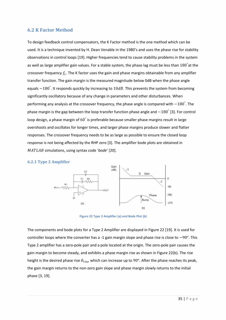
6.2.1 Type 2 Amplifier
Figure 22 Type 2 Amplifier (a) and Bode Plot (b)
The components and bode plots for a Type 2 Amplifier are displayed in Figure 22 [19]. It is used for
controller loops where the converter has a -1 gain margin slope and phase rise is close to . This
Type 2 amplifier has a zero-pole pair and a pole located at the origin. The zero-pole pair causes the
gain margin to become steady, and exhibits a phase margin rise as shown in Figure 22(b). The rise
height is the desired phase rise which can increase up to . After the phase reaches its peak,
the gain margin returns to the non-zero gain slope and phase margin slowly returns to the initial
phase [3, 19].
36 | P a g e
Equation 41 gives the Type 2 Amplifier transfer function by Ned Mohan. The Type 2 K factor is
calculated using Equation 42 [3, 19]. The pole and zero frequency of the controller transfer function
are based on the desired crossover frequency and the K factor value. This amplifier is suitable for
current control systems, and so can be used for designing the peak current compensator [3, 19].
Equation 41
Equation 42
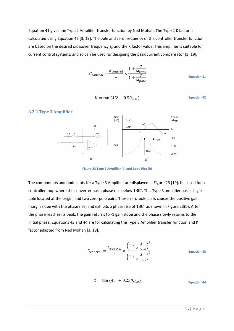
6.2.2 Type 3 Amplifier
R1
R2C1
C2
INOUT
+
-
Gain
(dB) -1
-1
+1
Phase
(deg)
0
-90
-180
-270
Gain
Phase
Rise
(a) (b)
R3C3
Figure 23 Type 3 Amplifier (a) and Bode Plot (b)
The components and bode plots for a Type 3 Amplifier are displayed in Figure 23 [19]. It is used for a
controller loop where the converter has a phase rise below . This Type 3 amplifier has a single
pole located at the origin, and two zero-pole pairs. These zero-pole pairs causes the positive gain
margin slope with the phase rise, and exhibits a phase rise of as shown in Figure 23(b). After
the phase reaches its peak, the gain returns to -1 gain slope and the phase slowly returns to the
initial phase. Equations 43 and 44 are for calculating the Type 3 Amplifier transfer function and K
factor adapted from Ned Mohan [3, 19].
Equation 43
Equation 44
37 | P a g e
6.3 Voltage mode control in Continuous Conduction Mode
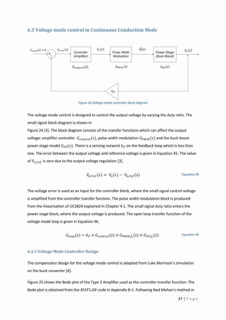
Figure 24 Voltage mode controller block diagram
The voltage mode control is designed to control the output voltage by varying the duty ratio. The
small signal block diagram is shown in
Figure 24 [3]. The block diagram consists of the transfer functions which can affect the output
voltage: amplifier controller , pulse width modulation and the buck-boost
power stage model . There is a sensing network on the feedback loop which is less than
one. The error between the output voltage and reference voltage is given in Equation 45. The value
of is zero due to the output voltage regulation [3].
Equation 45
The voltage error is used as an input for the controller block, where the small signal control voltage
is amplified from the controller transfer function. The pulse width modulation block is produced
from the linearisation of UC3824 explained in Chapter 4.1. The small signal duty ratio enters the
power stage block, where the output voltage is produced. The open loop transfer function of the
voltage mode loop is given in Equation 46.
Equation 46
6.3.1 Voltage Mode Controller Design
The compensator design for the voltage mode control is adapted from Luke Morrison’s simulation
on the buck converter [4].
Figure 25 shows the Bode plot of the Type 3 Amplifier used as the controller transfer function. The
Bode plot is obtained from the code in Appendix B-1. Following Ned Mohan’s method in
38 | P a g e
designing the feedback controller for voltage mode control, the desired phase rise is calculated using
the equations given below. The feedback path gain is [3].
Figure 25 MATLAB Bode Plot of Type 3 Amplifier Transfer Function
The absolute gain of the closed loop system is equivalent to 1 at the crossover frequency. It requires
the multiplication of the other transfer functions as given in Equation 47. While the feedback path
and PWM gain values are a constant ( , the crossover frequency
magnitude of the power stage needs to be converted from decibels to absolute value, as given in
Equation 48. The absolute controller transfer gain is calculated in Equation 49 [3].
Equation 47
Equation 48

39 | P a g e
Equation 49
Equation 50 is for calculating the control loop transfer function phase, which is obtained from the
power stage and feedback compensator transfer function. The PWM Gain and feedback path are not
included because both are constant values. Equation 51 ensures the control loop phase does not go
below with respect to the desired phase for loop stability. There is an angle of which is
compared with the phase rise for finding the phase angle in the controller transfer function
(Equation 52) [3].
Equation 50
Equation 51
Equation 52
It is possible to rearrange the equations in terms of the phase rise and calculate the value as given in
Equation 53.
Equation 53
According to H. Dean Venable, the maximum phase rise for the Type 3 Amplifier is at the
crossover frequency [19]. Since the phase rise for the voltage mode controller is less than and
above , the Type 3 Amplifier is the most suitable compensator for voltage mode control. The
maximum phase peak is , while the phase is for decreasing magnitudes. The controller
phase rise is the difference between the two phases, which is .
40 | P a g e
The K factor method is used to determine the pole and zero frequencies required to achieve the
desired controller phase rise. Using Equation 44 from Section 6.2.2, the K factor value is 7.396 as
given in Equation 54. The pole and zero frequencies can be calculated using the crossover frequency
and K factor, given in Equations 55 and 56. In the Bode plot, the pole and zero frequencies are the
points where the magnitude reaches its peak and the phase angle is near .
Equation 54
Equation 55
Equation 56
The frequencies calculated from Equations 55 and 56 are converted from to for
calculating Type 3 components (Equations 57 and 58). The Type 3 controller gain is calculated as
shown in Equation 59.
Equation 57
Equation 58
Equation 59
Using the values calculated, it is possible to perform calculations for the Type 3 resistors and
capacitors required for the voltage feedback compensator. is selected as the resistor value
for , while the other component values are calculated through Equation 60 to 64 [3].
41 | P a g e
Equation 60
Equation 61
Equation 62
Equation 63
Equation 64
Table 3 Type 3 Amplifier Parameters for Voltage Mode Control Implementation
42 | P a g e
6.4 Peak current control in Continuous Conduction Mode
The peak current mode compensator is designed to control the desired output voltage with the
inductor current. The current control block diagram is given in Figure 26. Unlike the
voltage mode control, the block diagram consists of the outer voltage loop and the inner current
control loop. The peak current mode block replaces the PWM block from the voltage mode loop [3,
21].
Controller
Peak Current
Mode
Controller
Power Stage
(Buck Boost)+-
Figure 26 Peak current mode controller block diagram
The slope compensation is the most unique feature of the peak current control. In Figure 27, the
desired inductor current is compared with the measured inductor current . Unlike the voltage
mode control, the current loop uses the slope compensation to limit the inductor current and
avoid oscillations produced from sub-harmonic frequencies. This is the case for duty ratios larger
than 0.5 [3].
0 t
Ts=1/fsTon
Toff
iL
iL*
ic
Slope Compensation
Figure 27 Peak Current Control with Slope Compensation
The DC reference perturbation will be zero since the regulated voltage is at a constant
level. The closed loop transfer function of the overall system is given in Equation 65 [3].
43 | P a g e
Equation 65
6.4.1 Peak current mode controller design
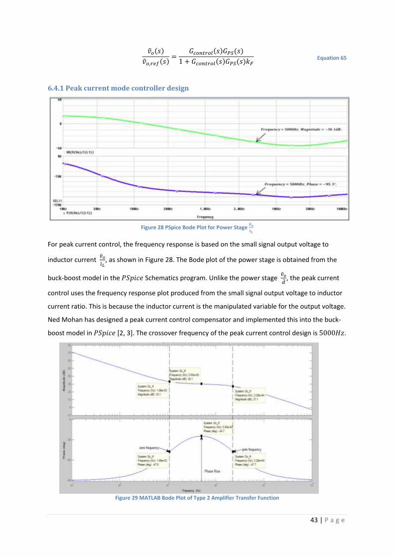
Figure 28 PSpice Bode Plot for Power Stage
For peak current control, the frequency response is based on the small signal output voltage to
inductor current
, as shown in Figure 28. The Bode plot of the power stage is obtained from the
buck-boost model in the Schematics program. Unlike the power stage
, the peak current
control uses the frequency response plot produced from the small signal output voltage to inductor
current ratio. This is because the inductor current is the manipulated variable for the output voltage.
Ned Mohan has designed a peak current control compensator and implemented this into the buck-
boost model in [2, 3]. The crossover frequency of the peak current control design is .
Figure 29 MATLAB Bode Plot of Type 2 Amplifier Transfer Function

44 | P a g e
The power stage magnitude and phase on the crossover frequency is and
respectively, as given in Figure 29. Based on the feedback loop from Figure 26, the peak current loop
transfer function is the product of the controller and power stage transfer function as given in
Equation 66. This makes the controller transfer function gain, as calculated in Equation 67.
Equation 66
Equation 67
Using the same phase margin from the voltage mode control and the crossover phase for
, the
phase rise of the current control is given in Equation 68. The Type 2 K factor value is calculated as
given in Equation 69. The pole and zero frequencies required for the desired phase rise is given in
Equations 70 and 71.
Equation 68
Equation 69
Equation 70
Equation 71
The frequencies calculated in Equations 72 and 73 are conversions from to for calculating
Type 2 components. The Type 2 controller gain is calculated using Equation 74.
Equation 72
Equation 73

45 | P a g e
Equation 74
Using the values calculated, it is possible to perform calculations for Type 2 resistors and capacitors
required for the voltage feedback compensator. is used for calculating the expected
parameters for the amplifier. A resistor is selected as the resistor value for , while the other
component values are calculated through Equations 75 to 77 [3].
Equation 75
Equation 76
Equation 77
These parameter values are used in designing the peak current control compensator, which is
connected to the Power Pole board and the model. The code in obtaining these
results is shown in Appendix B-2.
Table 4 Type 2 Amplifier Parameters for Peak Current Control Implementation
46 | P a g e
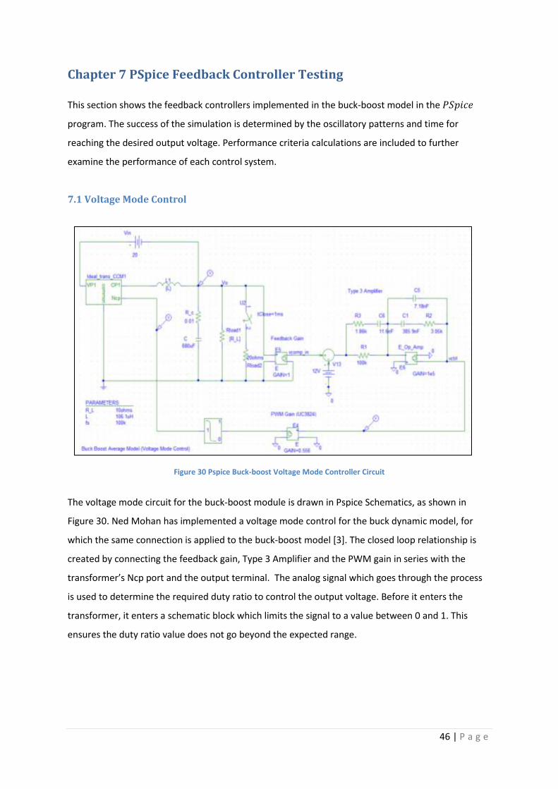
Chapter 7 PSpice Feedback Controller Testing
This section shows the feedback controllers implemented in the buck-boost model in the
program. The success of the simulation is determined by the oscillatory patterns and time for
reaching the desired output voltage. Performance criteria calculations are included to further
examine the performance of each control system.
7.1 Voltage Mode Control
Figure 30 Pspice Buck-boost Voltage Mode Controller Circuit
The voltage mode circuit for the buck-boost module is drawn in Pspice Schematics, as shown in
Figure 30. Ned Mohan has implemented a voltage mode control for the buck dynamic model, for
which the same connection is applied to the buck-boost model [3]. The closed loop relationship is
created by connecting the feedback gain, Type 3 Amplifier and the PWM gain in series with the
transformer’s Ncp port and the output terminal. The analog signal which goes through the process
is used to determine the required duty ratio to control the output voltage. Before it enters the
transformer, it enters a schematic block which limits the signal to a value between 0 and 1. This
ensures the duty ratio value does not go beyond the expected range.
47 | P a g e
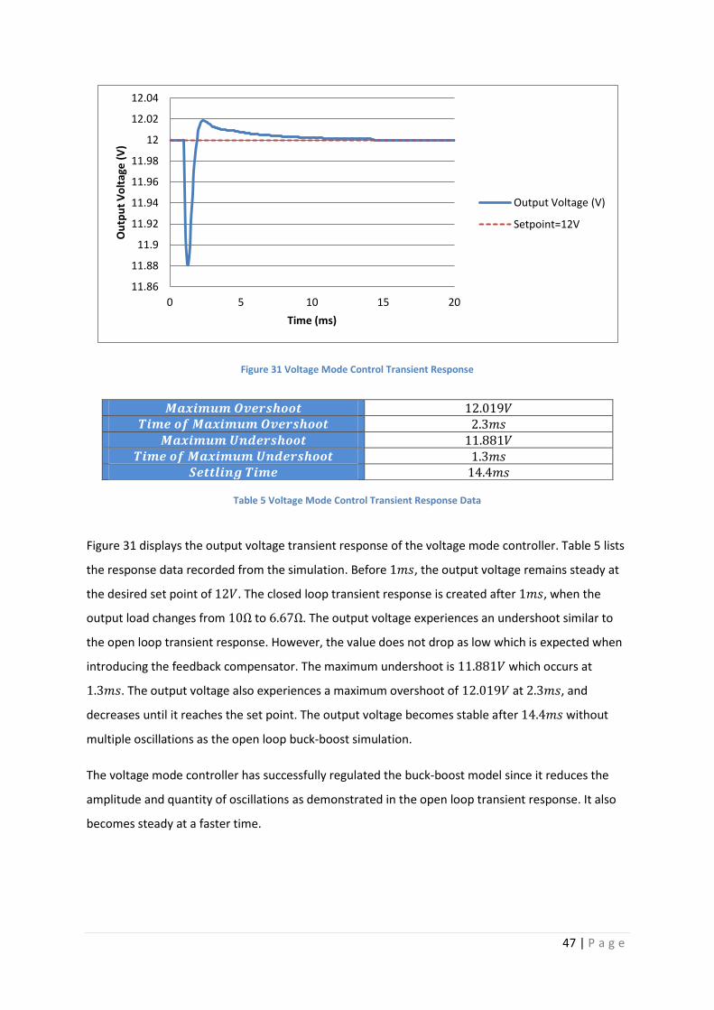
Figure 31 Voltage Mode Control Transient Response
Table 5 Voltage Mode Control Transient Response Data
Figure 31 displays the output voltage transient response of the voltage mode controller. Table 5 lists
the response data recorded from the simulation. Before , the output voltage remains steady at
the desired set point of . The closed loop transient response is created after , when the
output load changes from to . The output voltage experiences an undershoot similar to
the open loop transient response. However, the value does not drop as low which is expected when
introducing the feedback compensator. The maximum undershoot is which occurs at
. The output voltage also experiences a maximum overshoot of at , and
decreases until it reaches the set point. The output voltage becomes stable after without
multiple oscillations as the open loop buck-boost simulation.
The voltage mode controller has successfully regulated the buck-boost model since it reduces the
amplitude and quantity of oscillations as demonstrated in the open loop transient response. It also
becomes steady at a faster time.
11.86
11.88
11.9
11.92
11.94
11.96
11.98
12
12.02
12.04
0 5 10 15 20
Ou
tpu
t V
olt
age
(V
)
Time (ms)
Output Voltage (V)
Setpoint=12V
48 | P a g e
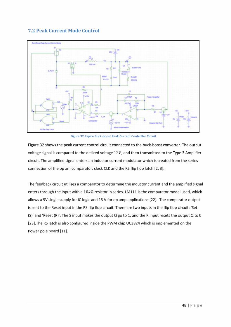
7.2 Peak Current Mode Control
Figure 32 shows the peak current control circuit connected to the buck-boost converter. The output
voltage signal is compared to the desired voltage , and then transmitted to the Type 3 Amplifier
circuit. The amplified signal enters an inductor current modulator which is created from the series
connection of the op am comparator, clock CLK and the RS flip flop latch [2, 3].
The feedback circuit utilises a comparator to determine the inductor current and the amplified signal
enters through the input with a resistor in series. LM111 is the comparator model used, which
allows a 5V single supply for IC logic and 15 V for op amp applications [22]. The comparator output
is sent to the Reset input in the RS flip flop circuit. There are two inputs in the flip flop circuit: ‘Set
(S)’ and ‘Reset (R)’. The S input makes the output Q go to 1, and the R input resets the output Q to 0
[23].The RS latch is also configured inside the PWM chip UC3824 which is implemented on the
Power pole board [11].
Figure 32 Pspice Buck-boost Peak Current Controller Circuit
49 | P a g e
Figure 33 Peak Current Control Transient Response
Table 6 Peak Current Control Transient Response Data
Figure 33 displays the peak current control transient response for the output voltage, and Table 6
lists the time and amplitude of the transient response. Since the ideal transformer and dynamic
model are not implemented for this feedback design, the converter experiences DC switching ripple.
This causes the inductor current to begin conduction from , thus the output voltage decreases
to at , and goes to the set point before . This behaviour is not included on Table
6 since it occurs before the transient response due to change in load. After , the peak current
circuit experiences a transient response because the output load change from to . This
makes the output voltage quickly decrease to at and quickly return to the set point
at .
The output voltage reaches to steady state, but there is a very small offset in the output voltage
compared to the desired set point. However, the offset can be neglected since the difference
is . It can be seen that the peak current control simulation is successful and produces faster
results than the voltage mode system.
11.92
11.93
11.94
11.95
11.96
11.97
11.98
11.99
12
12.01
0 1 2 3 4 5
Ou
tpu
t V
olt
age
(V
)
Time (ms)
Output Voltage (V)
Setpoint=12V

50 | P a g e
7.3 Performance Criteria Calculations Performance criteria calculations are used to further examine the efficiency of implementing
feedback controllers compared to the open loop model. Babatunde A. Ogunnaike and W. Harman
Ray published a book called “Process Dynamics, Modeling and Control”, which included calculations
of time integral performance criteria [24]. These calculations require the time integral error
produced from the process variables of dynamic systems. Both the Integral Absolute Error
and Integral Sum Error calculations enable the dynamic performance of each feedback
concept and the open loop system, as shown in Equations 78 and 79 [24]. The most effective
feedback controller which is analysed should have the smallest and .
Equation 78
Equation 79
Table 7 Control System Performance Criteria Values
Table 7 lists the performance criteria of each operating condition after the operating time. This
is the time when the buck-boost model experiences a transient event from the change in the output
load. Larger values are expected for the open loop transient response since it has more aggressive
oscillations overtime. Since the peak current control mode responds faster than voltage mode
control and possesses lower amplitude, it has smaller IAE and ISE values.
This provides further evidence proved that the peak current control mode gives the best
performance in the buck-boost simulation.
Chapter 8 – Power Pole Board
This chapter describes the components of the power pole board. The instructions for each
experiment are explained, which is required in order to obtain the results [1].
51 | P a g e
8.1 Technical Specifications
The Power pole Board is built by the University of Minnesota for educational learning of electronic
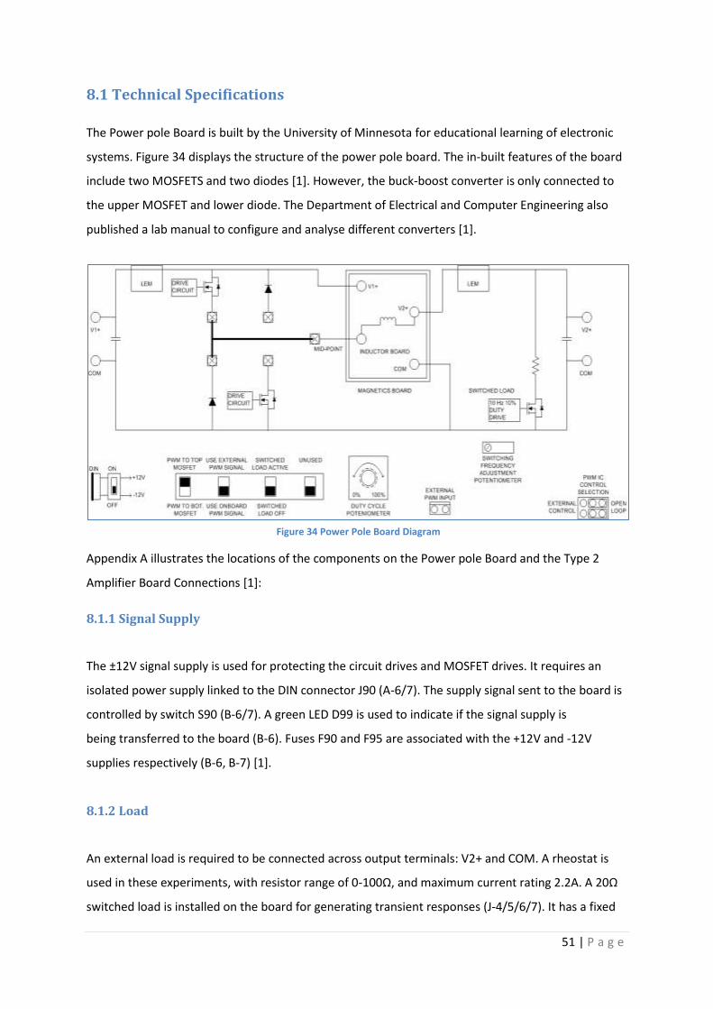
systems. Figure 34 displays the structure of the power pole board. The in-built features of the board
include two MOSFETS and two diodes [1]. However, the buck-boost converter is only connected to
the upper MOSFET and lower diode. The Department of Electrical and Computer Engineering also
published a lab manual to configure and analyse different converters [1].
Appendix A illustrates the locations of the components on the Power pole Board and the Type 2
Amplifier Board Connections [1]:
8.1.1 Signal Supply
The ±12V signal supply is used for protecting the circuit drives and MOSFET drives. It requires an
isolated power supply linked to the DIN connector J90 (A-6/7). The supply signal sent to the board is
controlled by switch S90 (B-6/7). A green LED D99 is used to indicate if the signal supply is
being transferred to the board (B-6). Fuses F90 and F95 are associated with the +12V and -12V
supplies respectively (B-6, B-7) [1].
8.1.2 Load
An external load is required to be connected across output terminals: V2+ and COM. A rheostat is
used in these experiments, with resistor range of 0-100Ω, and maximum current rating 2.2A. A 20Ω
switched load is installed on the board for generating transient responses (J-4/5/6/7). It has a fixed
Figure 34 Power Pole Board Diagram

52 | P a g e
frequency and duty ratio at 10Hz and 10% respectively. This makes it possible to periodically switch
in and out the load. The switched load is triggered by placing switch 3 of the selector switch
bank S30 to the top position (D/E-6) [1].
8.1.3 Frequency Analysis
It is possible to perform frequency response analysis in order to measure the transfer function
model of the configured board. This process is achieved by injecting a low voltage sinusoidal signal at
jumper J64 (F-6). The jumper J64 is removed from the converter and replaced by a small signal
sinusoidal source. The function generator is used to produce the small sinusoidal signal. The model
used is MFG-8216A (maximum frequency ), which is manufactured by Matrix [25]. In this
experiment, the frequency response will be measured over the range to .
8.1.4 Controller Selection Jumpers
The controller selection jumpers are J62 and J63 (H-6), which determines the power board operating
conditions. The board will operate in open loop mode before proceeding to closed loop mode. Both
jumpers must be on the right hand side for open loop configuration. For the Power board
experiment, peak current control will be used in the feedback compensator. When operating in
closed loop conditions, jumper J63 must be placed on the left side for external control [1].
8.1.5 Current Measurement
For peak current control mode, the current waveforms will be measured through the LEM current
sensors (B-1/2, I-1/2). The output current is located before the output filter capacitor, where the
oscilloscope probe is connected to CS5 and its ground to COM. The input current is located after the
input filter capacitor, where the oscilloscope probe can be connect to CS1 and its ground to COM.
Both sensors are calibrated so that 1A current flows through each, with 0.5V output. Signals are
scaled and connected to the daughter board connector J60. This allows feedback current control on
the board. Current sense resistors are used to measure currents flowing through MOSFETs and the
output capacitor [1].
8.1.6 PWM Signal Generation
PWM signals required for the MOSFETs can be generated using the on-board PWM controller

53 | P a g e
UC3824 (G-6). Although there is an alternative to supply PWM signals from an external source, this
thesis will only be using the onboard PWM for analysis. Switch 2 of the selector switch bank S30
allows the onboard PWM to be used by positioning the switch to its bottom position (D/E-6). The
duty ratio can be controlled using pot RV64 (E-6) when operating PWM in open loop mode. The duty
ratio can be varied from 4% to 98%. The trim pot RV60 (H-6) is used for adjusting PWM frequency.
For peak current control, there is a prerequisite for an external ramp to UC3824 IC. This is performed
by removing jumper J61 (G-6) and using the RAMP pin on the daughter board connector J60 (F/G/H-
7). It is important to note that J64 is short circuited for AC operation (F-6) [1].
8.2 Open Loop Operation in CCM
Before proceeding to closed loop or AC operation, it is important to set up the open loop
configuration to confirm buck-boost characteristics. The lab manual covers the instructions in
configuring the buck-boost module in CCM [1]. It is important to note that the input and output
ports are not connected in the same manner as the buck or boost converter. The laboratory
exercises involve the use of the following equipment:
1x Power Supply
1x Power pole Board
1x BB Magnetic Board
1x signal supply
1x Rheostat
2x Digital Multimeter (one for measuring output voltage, and the other for measuring
output current)
1x Oscilloscope
Multiple leads
Function generator (for transfer function analysis)
Below are the steps in constructing the buck-boost converter on the Power board [1].
1. Insert the BB Magnetics board required for buck-boost configuration. It is placed in the
middle of the power pole board.
2. Connect the rheostat and power supply to the board, as shown in Figure 35. Before the
connection, ensure the power supply voltage is and rheostat resistor is .
3. Connect the multimeters to measure output voltage and current flowing through the
rheostat.
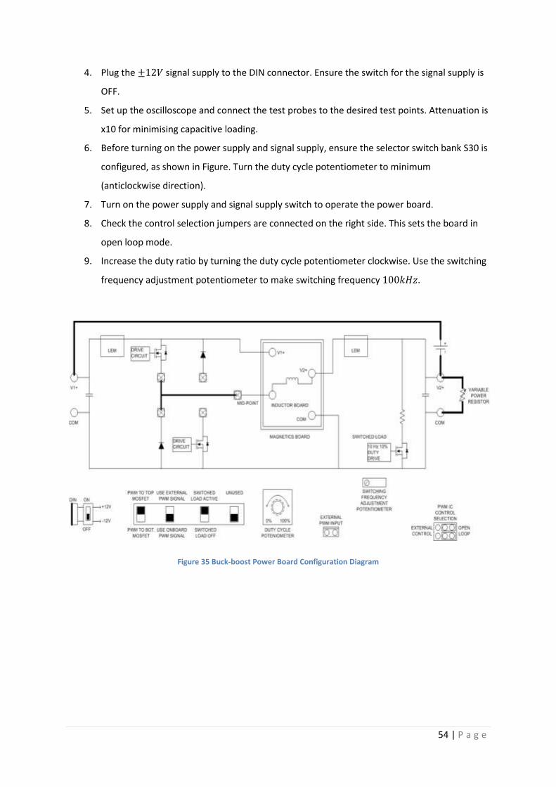
54 | P a g e
4. Plug the signal supply to the DIN connector. Ensure the switch for the signal supply is
OFF.
5. Set up the oscilloscope and connect the test probes to the desired test points. Attenuation is
x10 for minimising capacitive loading.
6. Before turning on the power supply and signal supply, ensure the selector switch bank S30 is
configured, as shown in Figure. Turn the duty cycle potentiometer to minimum
(anticlockwise direction).
7. Turn on the power supply and signal supply switch to operate the power board.
8. Check the control selection jumpers are connected on the right side. This sets the board in
open loop mode.
9. Increase the duty ratio by turning the duty cycle potentiometer clockwise. Use the switching
frequency adjustment potentiometer to make switching frequency .
Figure 35 Buck-boost Power Board Configuration Diagram

55 | P a g e
8.3 Finding the Transfer Function of the Buck-boost Power Board
This experiment is adapted from one of the lab exercises performed on the buck converter [1]. The
objective is to find the small signal frequency response for the buck-boost configuration. Here are
the steps in performing this exercise [1].
1. From the Open Loop Operation, make duty ratio at 0.5 and keep rheostat at .
2. Switch OFF the power supply and signal supply from the open loop operation.
3. Turn OFF the switched load on the selector switch bank.
4. Connect the function generator output and test probe to the small signal AC analysis
selection jumper J64. Make sure the polarity is connected properly.
5. Turn on the function generator and oscilloscope. Tune the function generator voltage to
sinusoidal output and peak-peak voltage.
6. Switch ON the signal supply and ensure the green LED light up. Turn ON the power supply to
.
7. Change the scope of the function generator voltage and output voltage to AC coupling.
8. Calculate the magnitude and phase difference between both waves. This is
completed by measuring the peak to peak voltage and delay time between the waves. The delay
time is the zero crossing gap for rising and falling time.
9. Repeat Step 8 until function generator frequency reaches .
8.4 Closed loop Operation (Peak current control mode)
The final task for the Power Board experiment is to observe how the peak current compensator
affects the buck-boost configuration. Here are the steps in performing this exercise [1].
1. Change the upper jumper from the control selection to the left side and leave the bottom
jumper in the same position. This will allow an external controller to be implemented into
the board.
2. Using the parameters calculated beforehand, position the resistors and capacitors for the
Type 2 Amplifier on a breadboard.
3. Remove the jumper from J61 and connect the breadboard to the daughter board connector.
This will introduce the feedback control for the board.
4. Turn the duty cycle potentiometer to the minimum position. Switch OFF the switched load.
5. Switch ON the signal supply before the power supply. Otherwise, the red LEDs will light up
for indicating technical issues.
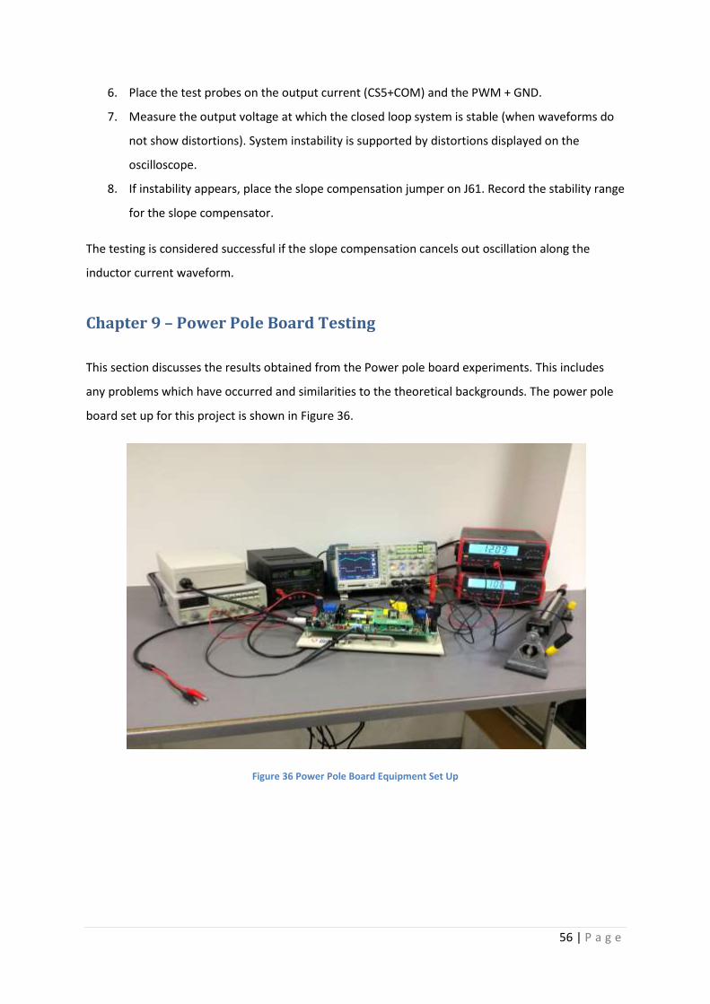
56 | P a g e
6. Place the test probes on the output current (CS5+COM) and the PWM + GND.
7. Measure the output voltage at which the closed loop system is stable (when waveforms do
not show distortions). System instability is supported by distortions displayed on the
oscilloscope.
8. If instability appears, place the slope compensation jumper on J61. Record the stability range
for the slope compensator.
The testing is considered successful if the slope compensation cancels out oscillation along the
inductor current waveform.
Chapter 9 – Power Pole Board Testing
This section discusses the results obtained from the Power pole board experiments. This includes
any problems which have occurred and similarities to the theoretical backgrounds. The power pole
board set up for this project is shown in Figure 36.
Figure 36 Power Pole Board Equipment Set Up

57 | P a g e
9.1 Buck-boost Transfer Function Findings
The transfer function magnitude and phase are displayed in Figures 37 and 38. The experimental
results are compared with the frequency response
. The results obtained from the Power
pole board were not expected since the buck-boost module does not experience a peak magnitude
produced by the two poles. Furthermore, the magnitude becomes constant at 0dB and the phase
does not reach lower than at higher frequency. As shown in the frequency response
simulation, the buck-boost converter should experience a magnitude gradient of
and phase angle of .
The function generator supplies an input voltage through jumper slot J64, which is also connected to
the UC3824 PWM chip in the Power Pole Board (pin number 15). Furthermore, the duty cycle pot
RV64 includes three resistors for controlling the duty ratio values. These connections are shown in
Appendix A-2. It is possible that these components cause problems in obtaining similar results to the
simulations.
Due to the failure in finding the locations of the poles and zeros on the Power pole board, it is
difficult to include these results into the final design of the feedback controllers and compare them
with simulation results.
Figure 37 Buck-boost Power Pole Board Magnitude Log Scale Plot
0.1
1
10
100
0 2000 4000 6000 8000 10000
Log
Frequency (Hz)
Buck Boost Frequency Response Magnitude Comparison (Log Scale)
Magnitude (PPB*)
Magnitude (Pspice)
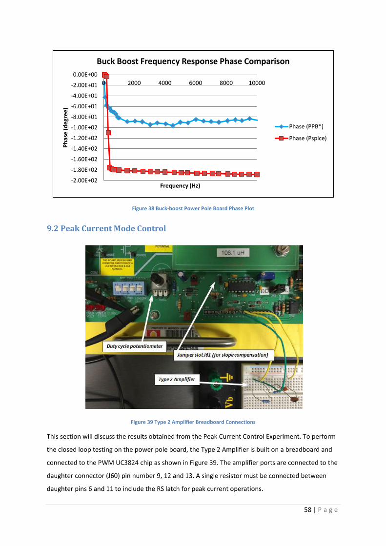
58 | P a g e
Figure 38 Buck-boost Power Pole Board Phase Plot
9.2 Peak Current Mode Control
Figure 39 Type 2 Amplifier Breadboard Connections
This section will discuss the results obtained from the Peak Current Control Experiment. To perform
the closed loop testing on the power pole board, the Type 2 Amplifier is built on a breadboard and
connected to the PWM UC3824 chip as shown in Figure 39. The amplifier ports are connected to the
daughter connector (J60) pin number 9, 12 and 13. A single resistor must be connected between
daughter pins 6 and 11 to include the RS latch for peak current operations.
-2.00E+02
-1.80E+02
-1.60E+02
-1.40E+02
-1.20E+02
-1.00E+02
-8.00E+01
-6.00E+01
-4.00E+01
-2.00E+01
0.00E+00
0 2000 4000 6000 8000 10000
Ph
ase
(d
egr
ee
)
Frequency (Hz)
Buck Boost Frequency Response Phase Comparison
Phase (PPB*)
Phase (Pspice)
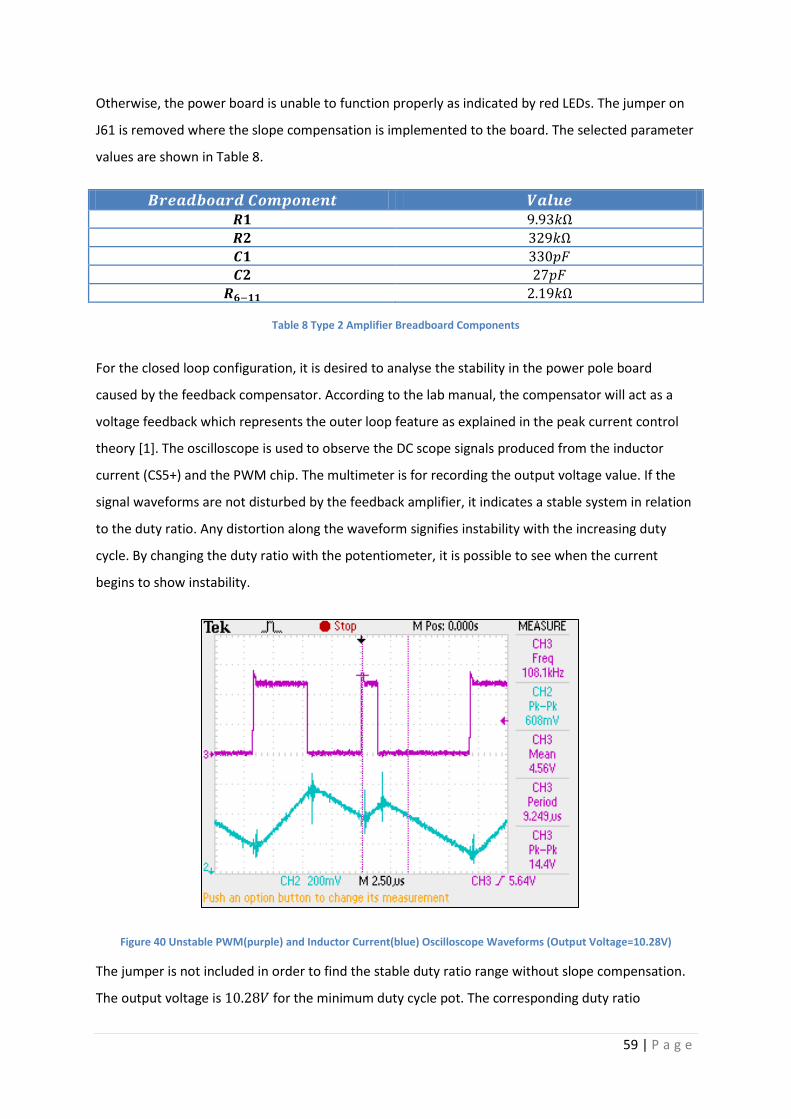
59 | P a g e
Otherwise, the power board is unable to function properly as indicated by red LEDs. The jumper on
J61 is removed where the slope compensation is implemented to the board. The selected parameter
values are shown in Table 8.
Table 8 Type 2 Amplifier Breadboard Components
For the closed loop configuration, it is desired to analyse the stability in the power pole board
caused by the feedback compensator. According to the lab manual, the compensator will act as a
voltage feedback which represents the outer loop feature as explained in the peak current control
theory [1]. The oscilloscope is used to observe the DC scope signals produced from the inductor
current (CS5+) and the PWM chip. The multimeter is for recording the output voltage value. If the
signal waveforms are not disturbed by the feedback amplifier, it indicates a stable system in relation
to the duty ratio. Any distortion along the waveform signifies instability with the increasing duty
cycle. By changing the duty ratio with the potentiometer, it is possible to see when the current
begins to show instability.
Figure 40 Unstable PWM(purple) and Inductor Current(blue) Oscilloscope Waveforms (Output Voltage=10.28V)
The jumper is not included in order to find the stable duty ratio range without slope compensation.
The output voltage is for the minimum duty cycle pot. The corresponding duty ratio

60 | P a g e
experiences instability as proved by the noise production from the inductor board
and the distorted waveforms displayed in Figure 40. The waveforms are distorted as each MOSFET
cycle is not identical.
As the duty cycle increases, the oscilloscope waveform becomes significantly distorted. However,
the power board begins to become stable at output voltage since the oscilloscope
waveforms are not disturbed. Furthermore, the inductor board produce minimal noise from the
current flow. The power pole board becomes unstable again for an output voltage greater than
. The stable duty ratio range without slope compensation is calculated in Equation 80.
Equation 80
The stability range of the buck-boost power board is very small. Without the slope compensation, it
is not possible to produce output voltages outside the calculated range. The slope compensation
jumper (Figure 41) is inserted onto for controlling the instability in the peak current output.
Table 9 lists the parameter values of the compensation jumper. The design concept of slope
compensation is to send a modified signal to the controller output, thus cancelling out oscillations.
This is especially important for duty ratios greater than . The outcome was expected as it cancels
out the fluctuations for the unstable values.
Figure 41 Slope Compensation Jumper
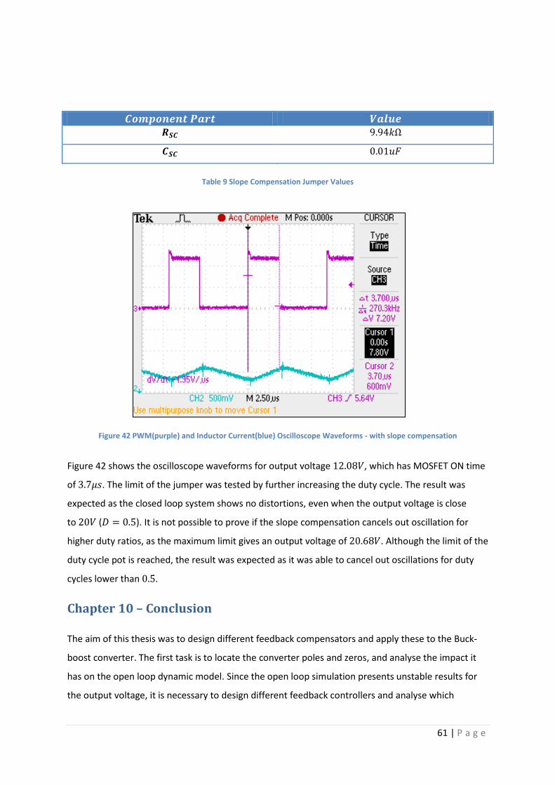
61 | P a g e
Table 9 Slope Compensation Jumper Values
Figure 42 PWM(purple) and Inductor Current(blue) Oscilloscope Waveforms - with slope compensation
Figure 42 shows the oscilloscope waveforms for output voltage , which has MOSFET ON time
of . The limit of the jumper was tested by further increasing the duty cycle. The result was
expected as the closed loop system shows no distortions, even when the output voltage is close
to ( ). It is not possible to prove if the slope compensation cancels out oscillation for
higher duty ratios, as the maximum limit gives an output voltage of . Although the limit of the
duty cycle pot is reached, the result was expected as it was able to cancel out oscillations for duty
cycles lower than .
Chapter 10 – Conclusion
The aim of this thesis was to design different feedback compensators and apply these to the Buck-
boost converter. The first task is to locate the converter poles and zeros, and analyse the impact it
has on the open loop dynamic model. Since the open loop simulation presents unstable results for
the output voltage, it is necessary to design different feedback controllers and analyse which

62 | P a g e
concept is more efficient. Both the voltage mode and peak current control utilise the K factor
method in completing the final design. feedback simulations are performed, for which both
feedback controllers give stable and quick responses. However, the peak current mode is the best
control system for the buck-boost converter, as calculated from IAE and ISE equations using
simulated data from the transient response. Therefore, the computer simulations show no difficulty
in completing one of the main objectives.
The power board experiments proved more challenging in completing the required task. Due to the
complexity of the hardware design, there was significant difficulty in finding the frequency response,
as evidenced from the noise production. This made it difficult for locating the poles and zeros on the
buck-boost configuration. When the peak current compensator was implemented, it was not
possible to test out the full extent in stability limit, as the hardware is configured between the
ranges of lower duty ratio.
In terms of producing different output values, the experimental results show that it is difficult to
produce other output voltages without the slope compensation jumper. This is because the inductor
current is not regulated which leads to unstable outputs. Once the jumper is connected with the
peak current control compensator, produce the desired output value similar to the peak current
control mode in simulations. This experiment further proves the theory of designing peak
current controllers for buck-boost converter.
Chapter 10.1 Future Work
For future work, it is possible to further improve the design of the buck-boost simulations and
hardware, as well as introducing a new concept to other types of converters. The peak current
control is commonly used in DC converters with RHP zero. The boost converter is another DC
converter, which features a RHP zero [26]. It would be interesting to analyse transient responses
produced from other converters. The power pole board allows an external PWM controller to be
connected through jumper J68 [1]. This will allow users to manually configure the power pole board
components to obtain better electronic performances. It is possible to perform circuit analysis using
other simulations packages. is another simulation program developed by MathWorks
,which performs block diagram analysis of dynamic systems [27]. It is possible to include the buck-
boost converter in this simulator with the linearised equations in Chapter 4.

63 | P a g e
References
[1] D. o. E. a. C. Engineering, Power Electronics Laboratory User Manual: University of Minnesota, 2004.
[2] N. Mohan. (2012). Educational Laboratories. Available: http://www.ece.umn.edu/~mohan/labs.html
[3] N. Mohan, Power Electronics: A First Course. Minneapolis: John Wiley & Sons, 2012. [4] L. Morrison, "Feedback Controller Design for Power Pole Electronics Laboratory Buck
Converter Module," Bachelor of Engineering, School of Engineering and Energy, Murdoch University, Murdoch, 2013.
[5] N. Mohan, T. M. Undeland, and W. P. Robbins, "Chapter 7: dc-dc Switch-Mode Converters," in Power Electronics: Converters, Applications, and Design 3rd ed., ed USA: John WIley & Sons, Inc, 2003, pp. 161-199.
[6] F. Semiconductor, "Characteristics of MOSFET" in AN-9010 MOSFET Basics, ed, 2000.
[7] E. Rogers, Understanding Buck-Boost Power Stages in Switch Mode Power Supplies, 2002. [8] Radio-Electronics.com. Capacitor ESR, Dissipation Factor, Loss Tangent and Q. Available:
http://www.radio-electronics.com/info/formulae/capacitance/esr-df-loss-tangent-q-tutorial-basics.php
[9] R. W. Erikson and D. Maksimović, Fundamentals of Power Electronics: Second Edition. Massachusetts: Kluwer Academic Publishers, 2001.
[10] R. King. (2004). The Ideal Transformer. Available: http://www.eng.utoledo.edu/~rking/IdealTrans.pdf
[11] (2007). High Speed PWM Controller. Available: http://www.ti.com.cn/cn/lit/ds/symlink/uc3824.pdf
[12] N. K. Gabriel A Rincón-Mora. (2006). Cloaking the non-idealities of DC-DC converter stability. Available: http://users.ece.gatech.edu/~rincon/publicat/trade_jrnls/pmdl_0106_dcdc_freq.pdf
[13] MathWorks. (2014). MATLAB: pzmap. Available: http://au.mathworks.com/help/control/ref/pzmap.html?nocookie=true
[14] R. M. N. J. David Irwin, "Application of the Laplace Transform to Circuit Analysis," in Basic Engineering Circuit Analysis, 10th Edition, ed USA: John Wiley & Sons, 2011, pp. 695-738.
[15] B. T. Lynch. Under the Hood of a DC/DC Boost Converter Available: http://www.ti.com/download/trng/docs/seminar/Topic_3_Lynch.pdf
[16] S. Maniktala. (2012). Voltage-Mode, Current-Mode (and Hysteretic Control). Available: http://www.microsemi.com/document-portal/doc_view/124786-voltage-mode-current-mode-and-hysteretic-control
[17] (2014). Electronic Systems. Available: http://www.electronics-tutorials.ws/systems/electronic-system.html
[18] (2014). Closed-loop Systems. Available: http://www.electronics-tutorials.ws/systems/closed-loop-system.html
[19] H. D. Venable, The K Factor: A New Mathematical Tool for Stability Analysis and Synthesis. Austin: Venable Industries, Inc., 1994.
[20] MathWorks. (2014). MATLAB: bode. Available: http://au.mathworks.com/help/ident/ref/bode.html
[21] M. K. Kazimierczuk, "Principle of Operation of PWM Converters with Peak-current-mode Control," in Pulse-width Modulated DC-DC Power Converters, L. John Wiley & Sons, Ed., ed Dayton, Ohio, USA: Wright State University, 2008, pp. 512-516.
[22] T. Instruments. (2013). LM111-N/LM211-N/LM311-N Voltage Comparator. Available: http://www.ti.com/lit/ds/symlink/lm111-n.pdf

64 | P a g e
[23] A. A. Circuits. (2014). The S-R Latch. Available: http://www.allaboutcircuits.com/vol_4/chpt_10/2.html
[24] W. H. R. Babatunde A. Ogunnaike, "Controller Design Principles," in Process Dynamics, Modeling, and Control, ed New York: Oxford University Press, Inc., 1994, pp. 519-524.
[25] Function Generator MFG8216A. Available: http://www.hestore.hu/files/MFG8216A.pdf [26] B. T. Lynch. Under the Hood of a DC/DC Boost Converter. Available:
http://www.ti.com/download/trng/docs/seminar/Topic_3_Lynch.pdf [27] MathWorks. (2014). Simulink. Available: http://au.mathworks.com/products/simulink/
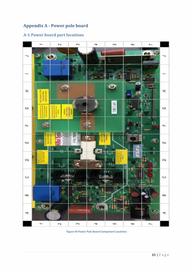
65 | P a g e
Appendix A - Power pole board
A-1 Power board part locations
Figure 43 Power Pole Board Component Locations
66 | P a g e
Number Components Ref. Des. Location in 1 Terminal V1+ J1 A-1
2 Terminal V2+ J21 J-1/2
3 Terminal COM (input) J2 A-4
4 Terminal COM (output) J22 J-7
5 DIN connector for ±12V signal supply J90 A-6/7
6 Signal supply switch S90 B-6/7
7 Signal supply +12V fuse F90 B-6
8 Signal supply -12V fuse F95 B-7
9 Signal supply LED D99 B-6
10 Fault LED D32 C-7
11 Over voltage LED D33 C-7
12 Over current LED D34 D-7
13 Upper MOSFET, diode and heat sink assembly Q15, D15 C-2/3
14 Lower MOSFET, diode and heat sink assembly Q10, D10 C-4/5
15 Screw terminal for upper MOSFET source J13 D-3
16 Screw terminal for lower diode cathode J11 D-4
17 Screw terminal for upper diode cathode J12 D/E-3
18 Screw terminal for lower MOSFET drain J10 D/E-4
19 Screw terminal for Mid-point J18 E-4
20 Magnetics Board with 106.1uH inductor J20 F/G/H-1/2/3/4/5
21 PWM Controller UC3824 U60 G-6
22 Duty ratio pot RV64 RV64 E-6
23 Switching frequency adjustment pot RV60 RV60 H-6
24 External PWM signal input terminal J68 F-7
25 Selector Switch Bank S30 D/E-6
26 Daughter board connector J60 F/G/H-7
27 Switched load R22 J-4/5/6/7
28 Resettable Fuse F21 J-2/3
29 Control selection jumpers J62, J63 H-6
30 Ramp select jumper J61 G-6
31 Current limit jumper J65 G-7
32 Small-signal ac analysis selection jumper J64 F-6
33 Input current sensor (LEM) CS1 B-1/2
34 Output current sensor (LEM) CS5 I-1/2
Table 10 Component locations on Power pole Board
67 | P a g e
Number Test Point Description of Test Point Location in
1 V1+ Terminal V1+ C-1
2 V2+ Terminal V2+ I/J-1
3 CS1 Input current B-4
4 CS2 Upper MOSFET source current D-3
5 CS3 Lower diode or lower MOSFET source current
D-5
6 CS4 Output Capacitor Current I-4
7 CS5 Output current I-5
8 CS LOAD 1 Switched Load Voltage +ve J-6
9 CS LOAD 2 Switched Load Voltage -ve J-6
10 PWM PWM signal D-7
11 DRAIN (upper MOSFET)
Upper MOSFET drain D-2
11 SOURCE (upper MOSFET)
Upper MOSFET source D-3
12 DRAIN (lower MOSFET)
Lower MOSFET drain E-5
12 SOURCE (lower MOSFET)
Lower MOSFET source E-5
13 ANODE (upper diode)
Upper diode anode E-2/3
13 CATHODE (upper diode)
Upper diode cathode E-2
14 ANODE (lower diode) Lower diode anode D-5
14 CATHODE (lower diode)
Lower diode cathode D-5
15 GATE (upper MOSFET)
Gate of upper MOSFET C-2/3
16 GATE (lower MOSFET)
Gate of lower MOSFET C-4/5
Table 11 Test points on the Power pole Board
68 | P a g e
A-2 Type 2 Amplifier Breadboard and PWM Connections
Figure 44 Power pole Board Circuit Drawing with Peak Current Control Board

69 | P a g e
Appendix B – MATLAB Code for Buck-boost Analysis and Controller
Design
B-1 Buck-boost Type 3 Amplifier Transfer Function % Voltage mode calculations for CCM Buck-Boost
clc s = tf('s');
% Buck-boost Converter Parameters Vin = 20; % Input voltage (V) r = 0.01; % Equivalent Series Resistance (ohm) C = 680 * (10^-6); % Capacitor (F) L = 106.1 * (10^-6); % Inductor (H) R = 10; % Resistor (ohm) = Output Load fs = 100 * (10^3); % Switching frequency (Hz)
% Input and Output Calculations Po = 18; % Output Power (W) Vo = 12; % Output Voltage (V) Io = Po/Vo; % Output Current (A) Iin = (Vo*Io)/Vin; % Input Current (A)
%Buck-boost Converter Duty Ratio D = Vo/(Vo+Vin);%1/((Vin/Vo)-1);
Le = L/((1-D)^2); %Small signal equivalent inductor kfb = 1; %Voltage feedback network
%-------------------------------------------------------------------- % PWM Linearisation (Controller UC3824) Vr = 1.8; %Peak to valley voltage G_PWM = 1/Vr; %PWM Gain unit %--------------------------------------------------------------------
% Step 1: Choose crossover frequency. fc = 1000;%Crossover frequency
% Step 2: Calculate required Phase Rise. % Desired phase margin ang_pm = 60; % degree
% Power Stage Angle at crossover frequency ang_gps = -179.2; % degree
% Required phase boost ang_rise = -90+ang_pm-ang_gps % degree
% Step 4: Calculate Kboost in radians. (Indicates geometric separation % between poles and zeros) Kboost = tand(45+(ang_rise/4))
% Calculate fz and fp using crossover frequency and Kboost. fz = fc/Kboost % Zero frequency (Hz) fp = Kboost*fc % Pole frequency (Hz)
70 | P a g e
wz = 2*pi*fz % Convert Hz to rad/s (Zero)
wp = 2*pi*fp % Convert Hz to rad/s (Pole)
%Power Stage Crossover Magnitude Gps_dB_fc = 18.2; Gps_fc = 10^(Gps_dB_fc/20);
G_ctrl_fc = 1/(G_PWM*Gps_fc*kfb)
k_ctrl = (wz*G_ctrl_fc)/Kboost
%Type 3 Amplifier Transfer Function G_ctrl = (k_ctrl/s)*(((1+(s/wz))^2)/((1+(s/wp))^2))
%Type 3 Amplifier Parameters R1 = 100*(10^3) C2 = wz/(k_ctrl*wp*R1) C1 = C2*((wp/wz)-1) R2 = 1/(wz*C1) R3 = R1/((wp/wz)-1) C3 = 1/(wp*R3)
bode(G_ctrl); %display bode plot of Type 3 Amplifier
B-2 Buck-boost Type 2 Amplifier Transfer Function
% Peak current control mode calculations for CCM Buck-Boost
clc s = tf('s');
%Buck-boost converter parameters Vin = 20; %Input voltage (V) r = 0.01; %Equivalent Series Resistance (ohm) C = 680 * (10^-6); %Capacitor (F) L = 106.1 * (10^-6); %Inductor (H) R = 10; %Resistor (ohm) = Output Load fs = 100 * (10^3); %Switching frequency (Hz)
% Step 1: Choose crossover frequency. fc = 5000;%Crossover frequency
% Step 2: Calculate required Phase Boost. % Desired phase margin ang_pm = 60;
% Power Stage Angle ang_gps = -95.3;
% Required phase boost ang_boost = -90+ang_pm-ang_gps
% Step 4: Calculate Kboost in radians. (Indicates geometric separation % between poles and zeros) Kboost = tand(45+(ang_boost./2))
% Calculate fz and fp using crossover frequency and Kboost.

71 | P a g e
fz = fc/Kboost % Zero frequency (Hz)
fp = Kboost*fc % Pole frequency (Hz) wz = 2*pi*fz % Convert Hz to rad/s (Zero) wp = 2*pi*fp % Convert Hz to rad/s (Pole)
% Power Stage Crossover frequency magnitude Gps_dB_fc = -30.1; Gps_fc = 10^(Gps_dB_fc/20);
Gc_fc = 1/Gps_fc
kc = wz/Gps_fc
% Type 2 Amplifier Parameter Equations R1 = 10*(10^3) C2 = wz/(wp*R1*kc) C1 = C2*(wp/wz-1) R2 = 1/(wz*C1)
% Type 2 Amplifier Transfer Function Gc_tf = (kc/s)*((1+s/wz)/(1+s/wp))
bode(Gc_tf) % Display bode plot of Type 2 Amplifier


![Bridgeless Buck-Boost PFC Converter for Multistring LED Driver€¦ · boost converter as a universal PFC converter [6]. In order to address these issues, a buck-boost converter is](https://img.pdfslide.net/doc/110x75/5eaabf2a4ab79d1e774f9005/bridgeless-buck-boost-pfc-converter-for-multistring-led-driver-boost-converter-as.jpg)