Embed Size (px)
Citation preview

1
Wolfgang Heinrich
Ferdinand-Braun-Institut (FBH),
Leibniz-Institut für Höchstfrequenztechnik
Berlin, Germany
Design and Characterization of Integrated
Circuits at Frequencies beyond 100 GHz
Acknowledgements
FBH, Berlin
Franz-Josef Schmückle, Adam Rämer, Siddartha Sinha
S. Chevtchenko, R. Doerner, M. Hrobak, M. Hossain, B. Janke, T. Jensen,
T. Krämer, V. Krozer, O. Krüger, I. Ostermay, A. Thies, G. Tränkle,
N. Weimann, J. Würfl
IHP, Leibniz-Institut, Frankfurt/Oder
Y. Borokhovych, J. Borngräber , M. Elkhouly, S. Glisic, M. Lisker, E. Matthus,
C. Meliani, B. Tillack, A. Trusch
Goethe Universität Frankfurt
M. Bauer, S. Boppel, V. Krozer, A. Lisauskas, M. Mundt,
H. G. Roskos
2

2
Beyond 100 GHz: The THz Frequency Range
Definition & physics
Part of electromagnetic spectrum from 0.1 THz to 10 THz
High propagation loss (interaction with molecules)
The challenges
Components difficult to realize (both electronic and optoelectronic ones)
Rather unexplored gap within the spectrum so far
The main applications (envisaged)
High-resolution radar, imaging, testing of materials
High data-rate (broadband) wireless communications
3
The THz Frequency Range
The THz paradoxon
No "killer application" on the horizon so far
Nevertheless: substantial funding and research activities worldwide
4

3
5 08.05.2014
Technological Gap at THz frequencies
Electronic approches
transit-time limited
Photonic approaches
limited by thermal energy
This Talk
Outline
Overview transistor technologies
InP-on-BiCMOS MMICs
Process development and technical challenges
Interconnects
Circuits
Plasmonics
Principle of operation
Detection & emission
THz challenges for em simulation
Conclusions
6

4
Transistor Technologies for 100+ GHz Frequencies (I)
InP heterobipolar transistors (HBTs)
Best efficient power amplifiers and up/down converters
90 mW (19.5 dBm) @ 220 GHz (0.25 µm emitter)
2 mW (2.8 dBm) @ 585 GHz (0.13 µm)
InP high electron-mobility transistors (HEMTs)
Best LNA results
Output power: 60 mW (17.8 dBm) @ 210 GHz (sub 50 nm gate)
Metamorphic HEMT (mHEMT)
InP-like properties on GaAs substrate
Future candidate: GaN HEMT
High breakdown but lower gain than InP and mHEMT
7
Transistor Technologies for 100+ GHz Frequencies (II)
CMOS
High functionality and integration density available
Continuous development (more Moore)
Limited output power: breakdown voltage scales with fmax
SiGe-BiCMOS
CMOS potential plus bipolars (more relaxed geometry than MOSFETs)
fmax close to III-V counterparts (500 GHz)
But lower power
1.3 mW (1 dBm) @ 245 GHz (130 nm SiGe BiCMOS)
8

5
Transistor Technologies for 100+ GHz Frequencies (III)
Summary
CMOS and SiGe-BiCMOS
high functionality and integration on-chip
essential, e.g., for radar/imaging arrays
limited in output power and noise figure
InP
best power and noise figure
limited integration capabilities
Why not combining the two technologies by heterogeneous integration?
Realizing digital and analog RF functionality on same chip
Idea convincing, but only minor-scale activities until recently
9
Heterogeneous Integration: Recent Progress
DARPA projects COSMOS/DAHI
Integrating InP bipolars with CMOS, on device level
Targeting high-speed circuits such as DACs
3 different approaches, 3 teams
(i) InP chiplets mounted on CMOS wafer
(Northrop Grumman Aerospace Systems)
(ii) Monolithically grown InP on Si wafer (Raytheon)
(iii) Epitaxial transfer and fabrication of InP HBTs on fully processed
CMOS wafer (HRL)
All 3 approaches successful, efforts ongoing
Major activities on mm-wave circuits > 100 GHz not known so far
10

6
This Work
Our Approach
Combine InP and BiCMOS not on device but on circuit level
Wafer-level process
Focusing on circuits in the frequency range 100 ... 500 GHz
Cooperation between FBH (InP) and IHP (BiCMOS)
2 Leibniz institutes located in Berlin and Frankfurt/Oder
11
Outline
Overview transistor technologies
InP-on-BiCMOS MMICs
Process development and technical challenges
Interconnects
Circuits
Plasmonics
Principle of operation
Detection & emission
THz challenges for em simulation
Conclusions
12

7
Process Flow (I)
13
SiGe-BiCMOS (IHP, Frankfurt)
0.25 µm technology,
fT/fmax = 180/220 GHz
8" wafers, fully processed
Alignment Marks
Si-BiCMOS Substrate
TM2
M3 M2 M1
TM1 Gd
InP substrate
Benzocyclobutene (BCB)
Wafer bonding
Dicing – cut into 4 x 3” Wafers
InP (FBH, Berlin)
0.8 µm DHBT
fT/fmax = 340/360 GHz
3” wafers, semi-processed
up to ground metal
Process Flow (II)
14
Remove InP Substrate SiO2
BCB
Au (Gd)
Al (TM2)
InP
Si
Si-BiCMOS Substrate
interconnects
SiO2
BCB
Au (Gd)
Al (TM2)
Alignment Marks
InP
Si
Si-BiCMOS Substrate
Au (G2) Interconnects InP-Si
Last metalization level
(G2)
E
E C
8
Challenges with InP-on-CMOS Integration
Compatibility between InP and BiCMOS process technologies
Join 8” (BiCMOS) and 3” (InP) wafers -> cutting
Ensure planar surfaces
Aluminum metallization (Si) meets gold metal (InP)
Wafer bonding
Alignment between wafers
Interconnects
Low RF insertion loss
Tolerate misalignment due to wafer bonding
Robust circuit design
Detuning of circuits due to stacked wafer structure
15
SiO2
BCB
Au (Gd)
Al (TM2)
Si-BiCMOS Substrate
Au (G2)
E C
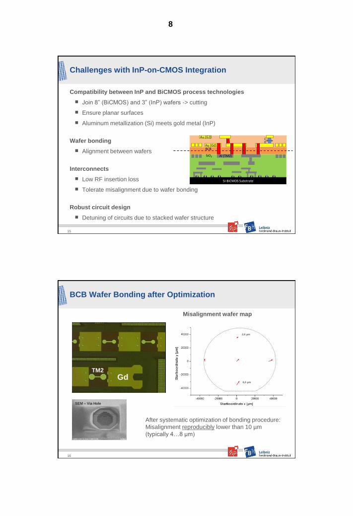
BCB Wafer Bonding after Optimization
Gd TM2
After systematic optimization of bonding procedure:
Misalignment reproducibly lower than 10 µm
(typically 4…8 µm)
SEM – Via Hole
2,6 µm
6,5 µm
Misalignment wafer map
16

9
Transmission Lines and Interconnects
Thin-film microstrip lines both in InP and BiCMOS parts
InP
G2 = signal line
Gd = ground
BiCMOS
TM2 = signal line
M1 = ground
Shielding by Gd avoids detuning of InP circuits
17
SiO2
BCB
Au (Gd)
Al (TM2)
Si-BiCMOS Substrate
Au (G2)
E
C
20 40 60 80 100 120-2.0
-1.5
-1.0
-0.5
0.0
@ 100 GHz
@ 200 GHz
S12 i
n d
B
Side length of the opening [µm]
Interconnect Design
Landing pad
Large enough to catch misalignment
But increases capacitance to GND
-> opening in ground
Stable optimum with high tolerance
to process variations
18
BiCMOS
InP InP

10
Interconnects: Measurements up to 220 GHz
Reflection and insertion loss of transition
Insertion loss < 0.3 dB per transition up to 110 GHz
< 0.5 dB up to 220 GHz
Excellent values (broadband)
Good agreement with simulations
19
40 80 120 160 200-50
-40
-30
-20
-10
0
S1
1 in
dB
frequency in GHz
Thru
420 µm
1250 µm
1950 µm
40 80 120 160 200-6
-5
-4
-3
-2
-1
0
S2
1 i
n d
B
frequency in GHz
Thru
420 µm
1250 µm
1950 µm
Interconnects: 220 … 325 GHz (I)
Test structure
Transition InP-BiCMOS as before
Daisy-chain with 10 transitions
Pad structure deembedded
in both em simulation and
measurements
20

11
220.000 230.000 240.000 250.000 260.000 270.000 280.000 290.000 300.000 310.000 320.000
freq [GHz]
-6.500
-6.000
-5.500
-5.000
-4.500
-4.000
-3.500
abs( Sxx ) (dB)
...29_hitek_thi02_trans_tm2_m1_d5_deduct: S(2,1)
tbottom3: S(2,1)
Interconnects: 220 … 325 GHz (II)
Transmission (S21): comparison em simulation with measurements
Deviations
less than 0.5 dB
up to 325 GHz
6.5 dB insertion loss
@ 325 GHz
for 10 transitions
(incl. line lengths)
< 0.5 dB
per transition
21
Circuit Design
Design process and tools used
Basic circuit topology
network-oriented approach equivalent-circuit models for active and
passive elements
2.5D em simulation for special structures, e.g. transformers
Optimization and layout
network description
check of critical layout parts by 2.5D (3D) em simulation
Interconnects & modules
design using 3D em simulation
Antennas
design by means of 3D em simulation
22

12
Circuit Results: Examples (I)
164 GHz hetero-integrated source
Output power: 0 dBm @ 164 GHz
3.2 x 1 mm² circuit size
82 GHz BiCMOS VCO InP Doubler + PA
164 GHz output
transition
23
Circuit Results: Examples (II)
246 GHz source
82 GHz VCO plus frequency tripler
Output power: -10 dBm
Phase noise: -87dBc/Hz @ 2 MHz offset
24

13
Summary InP-on-BiCMOS (I)
Technological achievements
Combining 8” SiGe-BiCMOS and 3” InP-HBT processes
Wafer bond alignment better than 10 µm
Broadband interconnects with low insertion loss
Below 0.5 dB @ 0 … 300 GHz
First circuits demonstrated
164 GHz and 246 GHz sources, oscillators at 200 GHz and 270 GHz
Outlook
Further stabilize process and establish seamless design environment
Increase output power
Downscale InP HBT emitter to push fmax > 500 GHz
25
Summary InP-on-BiCMOS (II)
Next step: modules
Flip-chip mounting of chips on AlN motherboard
Interconnect design by 3D em simulation
Passive test structures fabricated
26
view from backside

14
Flip-Chip Transition up to 400 GHz: Simulations (I)
Back-to-back structure with thru-line: E-field in the cross section
100 GHz
400 GHz
01/07/2012 27
Flip-Chip Transition up to 400 GHz: Simulations (II)
E-field: top view
100 GHz
400 GHz
radiation,
mainly generated
at the transitions
01/07/2012 28

15
Outline
Overview transistor technologies
InP-on-BiCMOS MMICs
Process development and technical challenges
RF results (interconnects)
Circuits realized so far
Plasmonics
Principle of operation
Detection & emission
THz challenges for em simulation
Conclusions
29
Plasmonics
Plasmon: quasi-particle resulting from quantization of plasma oscillations
Physical model
free electron plasma, e.g., in semiconductors
(partly) ballistic behavior of electrons
then: electron gas exhibits plasma waves (plasmons)
with a velocity beyond that of the electrons
Plasmonic effects allow operating a transistor structure beyond common cut-
off frequency fmax
30

16
31 08.05.2014
Transport in FETs: Dyakonov-Shur Description
0
v
x
U
m
e
x
vv
t
v
0
x
nv
t
n
Transport
equation:
Charge continuity:
Charge density dependence:
x-axis:
y-axis:
v
n
U Potential (voltage)
Charge density
Drift velocity
Scattering time M. Shur, T. A. Fjeldly, T. Ytterdal, and K. Lee,
Solid-state Electronics 35, 1795 (1992).
32 08.05.2014
Non-linear RLC Transmission Line Approximation
Harmonic analysis and approximation
to the first order yields the
transmission-line equations
with quantities (depending on
gate-to-channel voltage U)
Resistance
(Kinetic) inductance
Capacitance
I. Khmyrova and Y. Seijyou, Applied Physics Letters 91, 143515 (2007).

17
Plasmonic Devices for THz Applications
Plasmonic phenomena in FETs can be utilized for THz applications
in two different ways
Detectors
Effect proven experimentally for various structures
Particularly interesting: CMOS FETs
easy realization of detector arrays
integration with CMOS signal processing circuitry
Our approach: GaN instead of CMOS
Emitters
33
34 08.05.2014
Efficiency of Dyakonov-Shur-type mixing as a
function of frequency
EuMW2013
11 October, 2013
,,,
4
2
det sLfUU
UU
thgs
a
Ua: THz signal on gate
L: gate length
: momentum relaxation time
s: velocity of plasma waves
Quasi-static regime: No plasmonic mixing
Non-quasi-static regime: Distributed
resistive mixing (= plasmonic mixing in the
overdamped case) starts
Non-quasi-static regime: Full plasmonic
mixing (additional kinetic-inductance contribution is to
be included; enhances efficiency up to a factor
of three)
Dyakonov-Shur equations
predict an enhanced (!)
responsivity at higher frequencies
THz 2.3
1

18
Our Approach: GaN-Based Detectors
Technology
FBH 0.25 µm GaN MMIC process
HEMTs with small gate widths
w/o backside metal
First design
Bow-Tie antenna as receiving element (radiation from backside)
Direct coupling with double-HEMT configuration
Detection via drain bias current
35
36 08.05.2014
THz Emission from AlGaN/GaN HEMTs
State-of-the-art

19
37 08.05.2014
THz Emission from AlGaN/GaN HEMTs
• Gate (LW): 150/250 nm 2·100 μm
• THz emission for both; tunable only
with field plate, reason unknown
State-of-the-art From El Fatimy et al., JAP 107,
024504 (2010)
0.5 μm 3.15 μm
Without field plate
With field plate
Emitters: Our Approach
Objective
Prove measurements reported (on GaN)
Understand phenomena (e.g., impedance matching to antenna)
Design
Provide well-defined RF environment
ensure transistor stability from DC to fmax
Radiation into substrate,
dielectric lense on backside
Status
in process
38
1st-step detector structure

20
Outline
Overview transistor technologies
InP-on-BiCMOS MMICs
Process development and technical challenges
Interconnects
Circuits
Plasmonics
Principle of operation
Detection & emission
THz challenges for em simulation
Conclusions
39
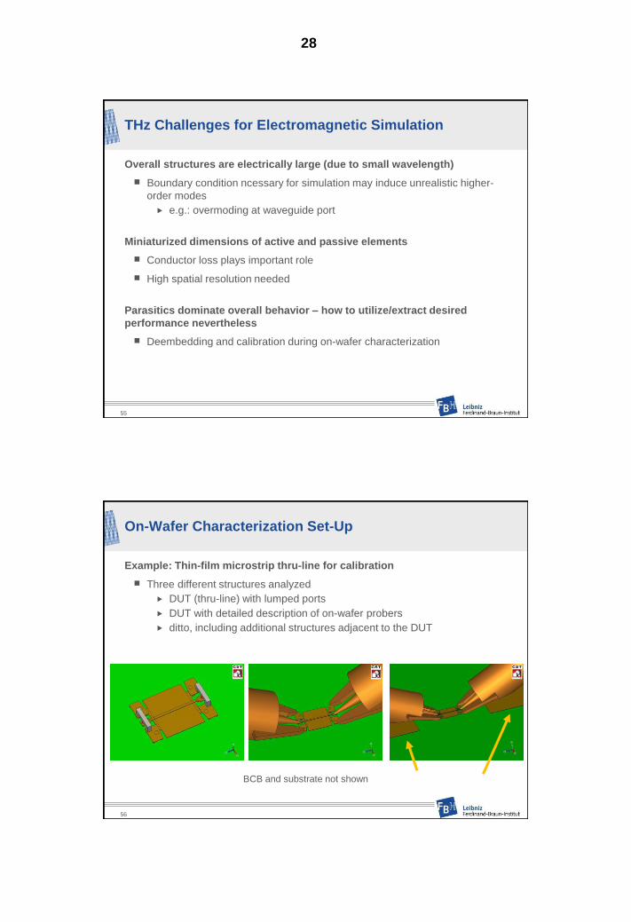
THz Challenges for Electromagnetic Simulation
Overall structures become electrically large (due to small wavelength)
Boundary conditions in simulation may induce unrealistic higher-order modes
e.g.: overmoding at waveguide port
40

21
Overmoding at Waveguide Ports (I)
Example: Electrically large CPW port with backside GND
Frequency range: 200…350 GHz
5 propagating modes detected
Includes higher-order modes due to artificial port boundary
41
600 µm
13 / 20 / 13 µm
ca. 2000 µm
Overmoding at Waveguide Ports (II)
Mode #1
Parallel-plate (PPL)
mode
realistic
42

22
Overmoding at Waveguide Ports (III)
Mode #2
Box mode due to
lateral port boundary
artificial
43
Overmoding at Waveguide Ports (IV)
Mode #3
Box mode due to
port boundaries
artificial
44

23
Overmoding at Waveguide Ports (V)
Mode #4
CPW mode
desired
45
Overmoding at Waveguide Ports (VI)
Mode #5
Higher-order
PPL mode
realistic,
but parasitic
46

24
Overmoding at Ports: What to do?
Use a (lumped) internal port
E.g.: CPW port with air-bridge to ensure proper excitation
Absorbing boundary condition at the outer boundaries
01/07/2012 47
THz Challenges for Electromagnetic Simulation
Overall structures are electrically large (due to small wavelength)
Boundary condition necessary for simulation may induce unrealistic higher-
order modes
e.g.: overmoding at waveguide port
Miniaturized dimensions of active and passive elements
Conductor loss plays important role
High spatial resolution needed
example: simulation of THz bow-tie antenna
48

25
Bow-Tie Antenna for THz (I)
The chip with the antenna (about 1 x 1 mm²) ...
49
Bow-Tie Antenna for THz (II)
Antenna (60 µm) with excitation by lumped port in the center (a few µm) ...
50
60 µm

26
Bow-Tie Antenna for THz (III)
Dielectric lens on the backside...
51
Bow-Tie Antenna for THz (IV)
Current density in y direction (at 1.5 THz)
52
y

27
Bow-Tie Antenna for THz (V)
Magnitude of E field in the x plane (cross-section)
53
Bow-Tie Antenna for THz (VI)
The Ez field in the dielectric lens (at 1.5 THz)
54
y
y
28
THz Challenges for Electromagnetic Simulation
Overall structures are electrically large (due to small wavelength)
Boundary condition ncessary for simulation may induce unrealistic higher-
order modes
e.g.: overmoding at waveguide port
Miniaturized dimensions of active and passive elements
Conductor loss plays important role
High spatial resolution needed
Parasitics dominate overall behavior – how to utilize/extract desired
performance nevertheless
Deembedding and calibration during on-wafer characterization
55
On-Wafer Characterization Set-Up
Example: Thin-film microstrip thru-line for calibration
Three different structures analyzed
DUT (thru-line) with lumped ports
DUT with detailed description of on-wafer probers
ditto, including additional structures adjacent to the DUT
56
BCB and substrate not shown

29
Simulations On-Wafer Measurement Set-Up (I)
Plots of E-field magnitude in longitudinal-section plane
57
Simulations On-Wafer Measurement Set-Up (II)
E-field magnitude (top view, plane 5 µm below the GND)
58

30
Conclusions (I)
Further development of electronics towards 1 THz frequency of operation
Si
CMOS: Limited advances (RF does not benefit from further downscaling)
SiGe-BiCMOS: further potential, limitations in output power will remain
III-V
InP: 1 THz within reach, strong activities in this field
Hetero-integration approaches will gain importance (system requirements)
Plasmonics
Interesting approach for frequency range exceeding 1 THz
Detectors
first arrays established, improvements to be expected
Emitter case: basics still to be clarified
59
Conclusions (II)
3D em simulation: indispensible tool for design
The THz designers' wish list regarding 3D em tools
High spatial resolution (this is a general trend)
Accurate conductor-loss description
True open boundary for both computational domain and ports
A particular challenge
Deembedding of on-wafer measurements
how to remove the strong influence of environment
60