Embed Size (px)
Citation preview
Design and Implementation of a High-speed Data Transmission System based on PCI-Express Protocol
Xing Yang Wu Qiong-zhi Department of complicated circuit system Department of complicated circuit system
Beijing Institute of Technology Beijing Institute of Technology Beijing China Beijing China
[email protected] [email protected]
Yang Xin-ran Su Fu-shun Department of complicated circuit system Department of complicated circuit system
Beijing Institute of Technology Beijing Institute of Technology Beijing China Beijing China
[email protected] [email protected]
Abstract - In order to meet the demand of high-speed digital data processing and achieve high-speed communication between digital front-ends and computer, we design and implement a transmission system based on FMC and PCI-Express protocol. This paper describes the basic hardware structure of the interface system, implements the high-speed data transmission via PCI-Express protocol on an FPGA and the highly modular design based-on FMC standard. The maximal speed of this transmission system is up to 34 Gbps. This system has a wide commonality as the communication interface module can be adjustable depending on different digital front-end.
Keywords – PCI-Express, digital front-end, FMC, modular
I. INTRODUCTION With the growing amount of digital signal processing and
its increasing speed development, how to achieve high-speed data transmission has become one of the emphases in the communication between digital front-end system and computer. PCI bus which was often used in the past cannot meet the requirements of high-speed data transmission system. So it is necessary to use a new data transmission technology. PCI-Express bus which is the newest generation of computer bus has represented the currently fastest solution to a point-to-point high-speed data transfer capability [1], the latest PCI-E 3.0 standard supports single-channel transmission rate of 8Gbps, up to 32 channels. Therefore, using the PCI-Express bus as the transmission interface between the digital front-end systems and computer has become an inevitable trend.
Because computer has fixed PCI-E interface, and there are many types of digital front-end system interface currently. It will generate a lot of resource waste if we design different transmission systems for each type of the digital front-end interface. We design a system using FMC modular technology [2]. FMC mezzanine card specification is defined in VITA 57 standard which is established by Xilinx. FMC's most obvious feature is to give up the traditional mezzanine card based on the characteristics of a standard bus, using a high-density and high-speed connection directly connected to the FPGA
programmable I/O. This article describes a high-speed data interface system of which the core controller is FPGA, external connection is FMC interface. This system transfers the large amounts of high-speed data with the computer through the PCI-E interface, through the FMC interface to improve system reusability.
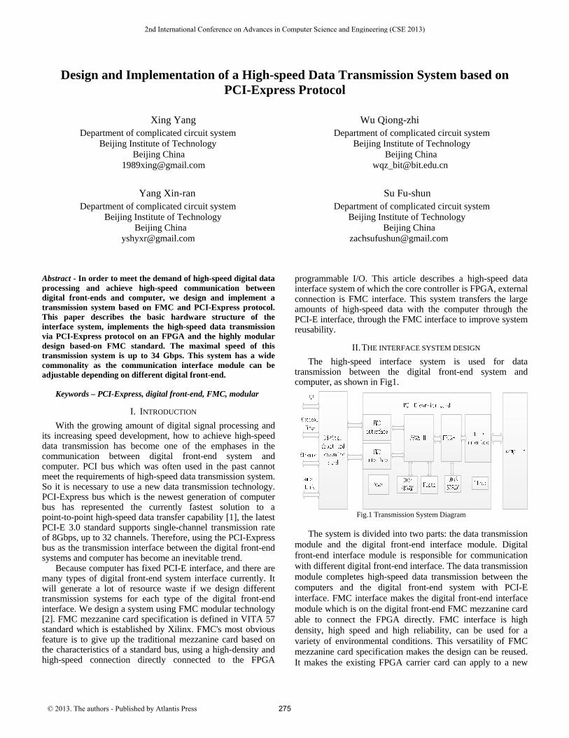
II. THE INTERFACE SYSTEM DESIGN The high-speed interface system is used for data
transmission between the digital front-end system and computer, as shown in Fig1.
Fig.1 Transmission System Diagram
The system is divided into two parts: the data transmission module and the digital front-end interface module. Digital front-end interface module is responsible for communication with different digital front-end interface. The data transmission module completes high-speed data transmission between the computers and the digital front-end system with PCI-E interface. FMC interface makes the digital front-end interface module which is on the digital front-end FMC mezzanine card able to connect the FPGA directly. FMC interface is high density, high speed and high reliability, can be used for a variety of environmental conditions. This versatility of FMC mezzanine card specification makes the design can be reused. It makes the existing FPGA carrier card can apply to a new
2nd International Conference on Advances in Computer Science and Engineering (CSE 2013)
© 2013. The authors - Published by Atlantis Press 275
data interface, with just changing the FMC module and slightly revamping the program of FPGA. The functionality of this module is completed by the PCI-E carrier card.
III. PCI-E CARRIER CARD PCI-E carrier card uses dual FPGA and dual FMC structure.
The FPGA adopts Virtex6-LX130T which is widely used currently and has rich I/O interface and internal logic resources. Two FMC interface can be equipped with different FMC mezzanine card according to different interface. FPGA-I is responsible for carrier card communication with the computer: controlling the PCI-E data transmission module and DDR3 SDRAM-for high-speed data cache. FPGA-II is responsible for the communication between the carrier card and FMC mezzanine card: control FMC module with various data front-end interface for data transmission, and a large capacity FLASH and a DDR3 SDRAM, for different rates of data cache. Data transmits with custom packet format between the two FPGA via chip bus. The transmission interface protocol is PCI-E 2.0 x8, theoretical transfers speed up to 40Gbps, taking into account the data codec expenses, the actual maximal speed up to 34Gbps.
The design of FPGA logic program can be divided into two parts: the PCI-E data transmission module of FPGA-I and the high-speed serial signal transmission module of FPGA-II.
A. The PCI-E data transmission module This module uses identifier in data transfer, including
registers transfer and stream data transfer. The parameter configuration of the digital front-end module is through register transfer. Stream data transfer complete large amount of data transmission.
This module uses the PCI-E transmission module to communicate with the computer and the DDR3 SDRAM as high-speed data cache [3].
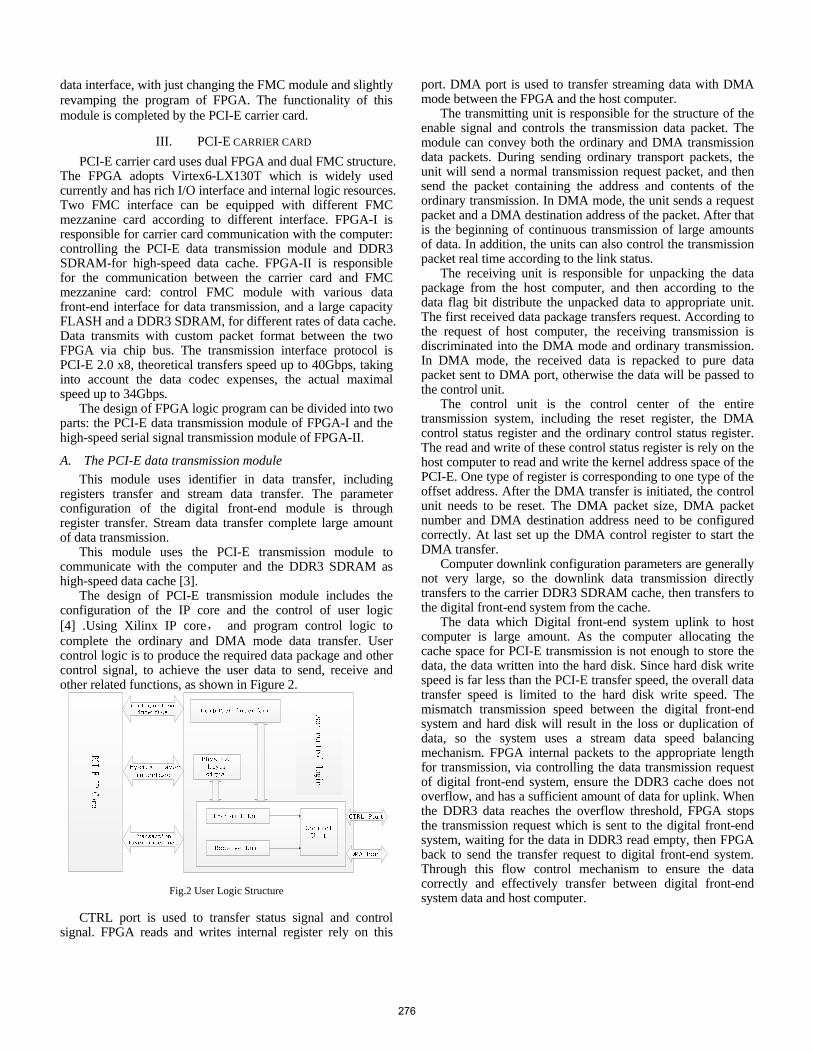
The design of PCI-E transmission module includes the configuration of the IP core and the control of user logic [4] .Using Xilinx IP core, and program control logic to complete the ordinary and DMA mode data transfer. User control logic is to produce the required data package and other control signal, to achieve the user data to send, receive and other related functions, as shown in Figure 2.
Fig.2 User Logic Structure
CTRL port is used to transfer status signal and control signal. FPGA reads and writes internal register rely on this
port. DMA port is used to transfer streaming data with DMA mode between the FPGA and the host computer.
The transmitting unit is responsible for the structure of the enable signal and controls the transmission data packet. The module can convey both the ordinary and DMA transmission data packets. During sending ordinary transport packets, the unit will send a normal transmission request packet, and then send the packet containing the address and contents of the ordinary transmission. In DMA mode, the unit sends a request packet and a DMA destination address of the packet. After that is the beginning of continuous transmission of large amounts of data. In addition, the units can also control the transmission packet real time according to the link status.
The receiving unit is responsible for unpacking the data package from the host computer, and then according to the data flag bit distribute the unpacked data to appropriate unit. The first received data package transfers request. According to the request of host computer, the receiving transmission is discriminated into the DMA mode and ordinary transmission. In DMA mode, the received data is repacked to pure data packet sent to DMA port, otherwise the data will be passed to the control unit.
The control unit is the control center of the entire transmission system, including the reset register, the DMA control status register and the ordinary control status register. The read and write of these control status register is rely on the host computer to read and write the kernel address space of the PCI-E. One type of register is corresponding to one type of the offset address. After the DMA transfer is initiated, the control unit needs to be reset. The DMA packet size, DMA packet number and DMA destination address need to be configured correctly. At last set up the DMA control register to start the DMA transfer.
Computer downlink configuration parameters are generally not very large, so the downlink data transmission directly transfers to the carrier DDR3 SDRAM cache, then transfers to the digital front-end system from the cache.
The data which Digital front-end system uplink to host computer is large amount. As the computer allocating the cache space for PCI-E transmission is not enough to store the data, the data written into the hard disk. Since hard disk write speed is far less than the PCI-E transfer speed, the overall data transfer speed is limited to the hard disk write speed. The mismatch transmission speed between the digital front-end system and hard disk will result in the loss or duplication of data, so the system uses a stream data speed balancing mechanism. FPGA internal packets to the appropriate length for transmission, via controlling the data transmission request of digital front-end system, ensure the DDR3 cache does not overflow, and has a sufficient amount of data for uplink. When the DDR3 data reaches the overflow threshold, FPGA stops the transmission request which is sent to the digital front-end system, waiting for the data in DDR3 read empty, then FPGA back to send the transfer request to digital front-end system. Through this flow control mechanism to ensure the data correctly and effectively transfer between digital front-end system data and host computer.
276
B. The high-speed serial signal transmission module The transmission between the carrier card and the digital
front-end system is through the high-speed data transmission module via the FMC interface.FMC specification define the signal grouping as the clock signal, the GTX signal and ordinary signal according to the FPGA I/O characteristics. So the GTX modules can be directly connected to high-speed serial signal of the FMC interface.
The high-speed Serial signal transmission uses the AURORA protocol [5] of Xilinx. After defining the GTX module of FPGA-II, Aurora IP core is called to code or decode the high-speed serial data with 8b/10b coding method, to embed or restore the serial data clock signal. Then get the conversion of parallel data and serial data completed through the operation of the clock calibration.
IV. DIGITAL FRONT-END FMC INTERFACE MEZZANINE CARD
Digital front-end FMC interface mezzanine card needs to be designed according to the digital front-end system interface, corresponding to different interfaces which are needed to design different mezzanine card. At present, the system has been applied to two different mezzanine card, using the optical interface and Camera Link interface.
A. Optical fiber mezzanine card The optical fiber interface FMC mezzanine card uses SFP
module [6] as the transmission platform of a miniature synthetic aperture radar system. Because the front-end system requires a long-distance transmission, using the smaller loss optical fiber as a data transmission interface. The SFP module on the mezzanine card is FTLF8519P3ByL multi-mode photoelectric conversion module, 850nm transmission wavelength, the longest transmission distance 500 meters, are connected to the FPGA-Ⅱ GTX high-speed serial module through the FMC. Data transfer protocol is AURORA protocol, 8b/10b codec. Theoretical transfer speed is up to 2.125Gbps, the actual transfer speed is up to 1.5Gbps.
B. Codec mezzanine card Codec mezzanine card codes and decodes the transmission
data between aerial camera and FPGA with 8b/10b coding method. The TLK 4711 is an 8b/10b codec; encoding and decoding the transmission data with 8b/10b coding method. The mezzanine card interface for the front-end system is the Camera Link, dedicated camera and image interface, theoretical speeds up to 6.8Gbps, but poor reusability to other digital devices. This design of the transmission system saves a lot of resources, greatly improves the reusability of the design.
V. SYSTEM IMPLEMENTATION AND PERFORMANCE TESTING
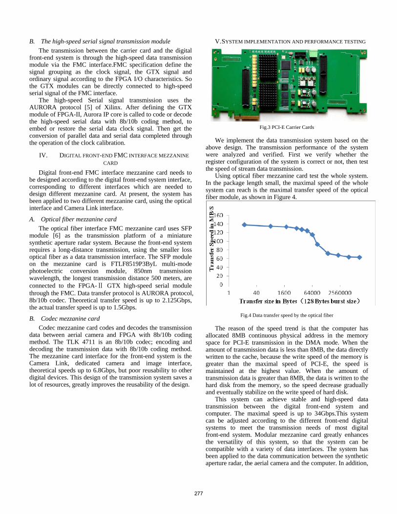
Fig.3 PCI-E Carrier Cards
We implement the data transmission system based on the above design. The transmission performance of the system were analyzed and verified. First we verify whether the register configuration of the system is correct or not, then test the speed of stream data transmission.
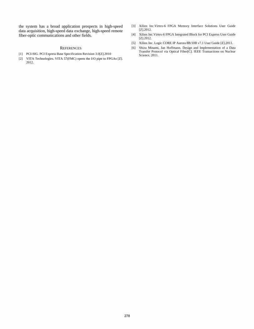
Using optical fiber mezzanine card test the whole system. In the package length small, the maximal speed of the whole system can reach is the maximal transfer speed of the optical fiber module, as shown in Figure 4.
Fig.4 Data transfer speed by the optical fiber
The reason of the speed trend is that the computer has allocated 8MB continuous physical address in the memory space for PCI-E transmission in the DMA mode. When the amount of transmission data is less than 8MB, the data directly written to the cache, because the write speed of the memory is greater than the maximal speed of PCI-E, the speed is maintained at the highest value. When the amount of transmission data is greater than 8MB, the data is written to the hard disk from the memory, so the speed decrease gradually and eventually stabilize on the write speed of hard disk.
This system can achieve stable and high-speed data transmission between the digital front-end system and computer. The maximal speed is up to 34Gbps.This system can be adjusted according to the different front-end digital systems to meet the transmission needs of most digital front-end system. Modular mezzanine card greatly enhances the versatility of this system, so that the system can be compatible with a variety of data interfaces. The system has been applied to the data communication between the synthetic aperture radar, the aerial camera and the computer. In addition,
277
the system has a broad application prospects in high-speed data acquisition, high-speed data exchange, high-speed remote fiber-optic communications and other fields.
REFERENCES [1] PCI-SIG. PCI Express Base Specification Revision 3.0[Z].2010 [2] VITA Technologies. VITA 57(FMC) opens the I/O pipe to FPGAs [Z].
2012.
[3] Xilinx Inc.Virtex-6 FPGA Memory Interface Solutions User Guide [Z].2012.
[4] Xilinx Inc.Virtex-6 FPGA Integrated Block for PCI Express User Guide [Z].2012.
[5] Xilinx Inc. Logic CORE IP Aurora 8B/10B v7.1 User Guide [Z].2011. [6] Shizu Minami, Jan Hoffmann. Design and Implementation of a Data
Transfer Protocol via Optical Fiber[C]. IEEE Transactions on Nuclear Science, 2011.
278