Embed Size (px)
Citation preview

DESIGN AND IMPLEMENTATION OF
A SINGLE PHASE SYMMETRICAL
HYBRID SINUSOIDAL PULSE WIDTH
MODULATED INVERTER
Ismot Tasmary Salsabil
Department of Electrical & Electronic Engineering
Dhaka University of Engineering & Technology, Gazipur
November 2016

i
DESIGN AND IMPLEMENTATION OF
A SINGLE PHASE SYMMETRICAL
HYBRID SINUSOIDAL PULSE WIDTH
MODULATED INVERTER
A dissertation submitted in partial fulfillment of the requirements for
the degree of
Master of Engineering in Electrical & Electronic
Engineering
By
Ismot Tasmary Salsabil
Student No. 092234
Under Supervision of
Dr. Md. Raju Ahmed
Professor, Dept. of EEE
Department of Electrical & Electronic Engineering
Dhaka University of Engineering & Technology, Gazipur
November 2016

iii
Declaration
I declare that this thesis is my own work and has not been submitted in any form for another
degree or diploma at any university or other institute of tertiary education. Information
derived from the published and unpublished work of others has been acknowledged in the
text and a list of references is given.
Ismot Tasmary Salsabil Date: 21 /11/2016

Acknowledgements
First of all, I thank the Almighty, who gave me the opportunity and strength to carry out
this research work.
I would like to express my sincere gratitude and profound indebtedness to my supervisor
Dr. Md. Raju Ahmed for constant guidance, insightful advice, helpful criticism, valuable
suggestions, commendable support and endless patience towards the completion of this
thesis. I feel very proud to have worked with him. Without his inspiring enthusiasm and
encouragement, this work could not have been completed.
I am deeply indebted and grateful to Professor Dr. Md. Shaheen Hasan Chowdhury,
Head, Department of EEE, Dhaka University of Engineering and Technology, Gazipur, for
his encouragement and supports throughout thesis work.
I thank all my teachers and staffs at the Department of EEE, Dhaka University of
Engineering and Technology for their support and encouragement.
I wish to express my gratitude to Dhaka University of Engineering and Technology,
Gazipur for providing an excellent environment for research. The support I have received
from Dhaka University of Engineering and Technology is gratefully acknowledged.
I would like to express my most sincere gratitude to my family, my friends and well
wishers who are taking lot of pains for progress in my life and for their sacrifices, blessings
and constant prayers for my advancement.
Finally, last but not least, I am also thankful to those, who have directly or indirectly helped
me and encouraged me to complete my thesis. I feel sorry for not able to express my
appreciation to each of my well-wishers and ask forgiveness for my improper behavior with
anyone who was intending to help me.
iv

v
Abstract
The Inverter is widely used for various applications such as speed control of AC motors,
photovoltaic interface, flexible AC transmission system (FACTS) and power conditioning
devices. Inverters are consists of four switches they are operated by power frequency
switching signal or pulse width modulated (PWM) high frequency switching signal.
In the Square wave inverter the switches are drives by low frequency switching signals.
The output contains a large amount of lower order harmonics. To reduce these harmonics a
large bulky filter is required. In this type of inverter the switching loss is negligible as
compared to conduction loss because of low frequency switching.
The PWM techniques-Four switches are operated at high frequency then the output
frequency. In this case the output consist harmonics of high frequency (switching frequency
and its odd multiple). The switching loss is increased due to high frequency switching. A
small filter is required at the output to get sinusoidal output. Output consist harmonics of
high frequency the switching loss of a switch is the summation of turn on loss, turn off loss
and conduction loss.
The Hybrid PWM-In this techniques two switches operated by high frequency PWM
switching signals and two switches drives by low output frequency signals. The switches
driven with high frequency causes higher switching loss compared to the switches driven
with low frequency switching signals. The unequal temperature rise at the switches
operated by high frequency and decreases the reliability of the system. This reduces the
overall switching loss to nearly half.
The Proposed symmetrical hybrid sine PWM (SHSPWM)-To overcome these
drawbacks, Symmetrical Hybrid Sine PWM (SHSPWM) technique is invented where each
switch operated at high frequency and low frequency alternatively and at any time two
switches operated at high frequency and two switches operated at low frequency. Therefore,
the total switching loss becomes half and equally distributed among the all switches.
Switching loss of all four switches are same which improve the reliability.

vi
The Square wave inverter is simulated first using ORCAD simulation software, and then
PWM inverter after that HSPWM inverter is simulated and finally proposed SHSPWM
modulated inverter is designed and simulated. In every case the performance of the inverter
in terms of the total harmonics distortion (THD) and efficiency is analyzed. For generation of the
switching signals comparators are used. Simple logic gates are used to generate the
SHPWM switching signal from the high frequency and low frequency switching signals.
Finally, the proposed SHSPWM inverter is implemented in the laboratory and performance
is analyzed. In practical implemented circuit IGBT is used as switching devices to reduce
the switching loss. IGBTs are a new technology that replaces MOSFETs. IGBT is
combination of both MOSFET and BJT in monolithic form. BJTs have high current handling
capacity and MOSFET is easy to control, IGBTs are better performing for medium to high voltage
applications. The efficiency of the implanted SHSPWM inverter is analyzed varying the
input voltage and output load.

Abbreviations
Abbreviation Full Meaning
EMI Electromagnetic Interference.
SMPS Switch Mode Power Supply.
BJT Bipolar Junction Transistor.
MOSFET Metal Oxide Semiconductor Field Effect Transistor.
IGBT Insulated Gate Bipolar Transistor.
PWM Pulse Width Modulation.
OPAMP Operational Amplifier.
SCR Silicon Control Rectifier.
GTO Gate Turn Off SCR.
Rms Root mean square.
IG Isolated ground.
HPWM Hybrid Pulse Width Modulation.
HVDC High voltage direct current.
VSI Voltage source inverter
CSI Current source inverter
vii
TABLE OF CONTENTS
Chapter 1: Introduction
1.1 Introduction 1
1.2 Early Analysis of Inverter Response 2
1.3 Recent work 3
1.4 Specific Aims of the Thesis 4
1.5 Outline of the thesis 5
Chapter 2: Theory of Inverter
2.1 Introduction 7
2.2 Application of inverter 7
2.2.1 Un interruptible Power Supply 7
2.2.2 Induction heating 8
2.2.3 High voltage direct current (HVDC) Power transmission 8
2.2.4 Variable frequency drives 8
2.2.5 Electric vehicle drives 8
2.3 Classification of inverters 9
2.3.1 Operation of single phase inverter
9
2.3.2 Square wave PWM 10
viii
Page No.
Title page i
Board of examiners ii
Declaration iii
Acknowledgement Iv
Abstract v
Abbreviations vi
List of contents vii
List of Figures xi
List of Table xiii

2.4 Voltage control of single phase inverter 10
2.4.1 Single pulse width modulation (Single PWM) 10
2.4.2 Multiple pulse width modulation 11
2.4.3 Sinusoidal pulse width modulation 11
2.5 Inverters are classified according to the type of input applied 12
2.5.1 Voltage source inverter (VSI) 12
2.5.2 Current source inverter (CSI) 12
2.5.3 Variable DC linked inverter 13
Chapter 3: Design and Analysis of SHSPWM (Symmetrical Hybrid
Sine Pulse Width Modulation) Inverter.
3.1 Introduction 14
3.2 Square wave inverter 14
3.2.1THD(Total Harmonics Distortion) calculations 16
3.3 PWM Inverter
3.3.1THD(Total Harmonics Distortion) calculations
17
3.4 HSPWM Inverter Design 20
3.5 SHSPWM Inverter design 22
3.5.1 Step 1PWM signal generation. 22
3.5.2 Step 2 Square wave signal generation. 24
3.5.3: Step 3 : generating low and high voltage signals. 24
3.5.4: Step 4: generating high and low signal together. 26
3.5.5: Step 5: generating four gate signals. 28
3.5.6: Step 6: generating four gate signals using optocoupler. 29
3.5.7: Step 7: Designing SHSPWM Inverter without filtering. 31
3.5.8: Step 8: Filter Design for reduce harmonics. 34
3.6:Results 36
ix

Chapter 4:Implementation of SHSPWM Inverter
4.1 Experimental setup 38
4.1.1 Elements used for practically implemented circuit 44
4.2 Experimental results 51
Chapter 5:Conclusion and Recommendation
5.1 Conclusion 52
5.2 Recommendation for future work 53
REFFERENCES 54
X

LIST OF FIGURES
3.1 Starting of ORCAD software. 14
3.2 The circuit diagram of square wave inverter. 15
3.3 The output wave shape of square wave inverter (Taking from R1). 15
3.4 Frequency spectrum diagram for square wave inverter 16
3.5 The circuit diagram of PWM inverter. 18
3.6 The frequency spectrum for PWM inverter 19
3.7 The circuit diagram of HSPWM inverter.
20
3.8 The circuit diagram of HSPWM inverter with output filtering 21
3.9 The output wave shape of HSPWM inverter. 21
3.10 The frequency spectrum for HSPWM inverter 22
3.11 PWM signal generation circuit. 23
3.12 The output waveshape from IC AD648C. 23
3.13 Square wave signal generation from IC AD648C. 24
3.14 The circuit diagram for generating low and high frequency switching
signals
24
3.15 The output voltage waveform of (a) low frequency inverting signal, (b)
low frequency non-inverting signal.
25
3.16 The output voltage waveform of (a) high frequency inverting signal, (b)
high frequency non-inverting signal.
26
3.17 Circuit diagrams of D-flip flop 27
3.18 The circuit for mixing low and high frequency switching signal together
with the help of flip-flop.
27
3.19 The input and output waveform from flip-flop IC 74HC74 28
3.20 The circuit diagram for generating four gate signals 29
3.21 A basic circuit diagram using optocoupler, b) typical output voltage
waveforms of optocoupler.
30
3.22 The circuit diagram for generating four gate signals using optocoupler. 31
3.23 Final circuit diagram of the SHSPWM Inverter without filtering 32
3.24 Block diagram of an output filter design 34
3.25 Final circuit diagram of the SHSPWM Inverter after filtering the inverter 35
3.26 Output voltage wavefrom of the proposed SHSPWM inverter after
filtering
xi
35

3.27 The frequency spectrum of output of SHSPWM inverter after filtering 36
4.1 Picture of practically implemented SHSPWM Full circuit 39
4.2 Picture of practically implemented SHSPWM inverter in working mode. 40
4.3 Picture of the controlling circuit of implemented circuit showing its
different components.
40
4.4 Picture of controlling circuit showing different parts 40
4.5 Output sine voltage waveforms from IC L8038 sine wave generator, when
input frequency 50KHz.
44
4.6 Output triangular voltage waveforms from IC L8038 triangular wave
generator, when input frequency 4KHz.
45
4.7 Output low frequency switching signal of frequency 50 Hz 45
4.8 Output PWM switching signal of frequency 4 kHz. 45
4.9 Output High switching signal of frequency 4 kHz 46
4.10: Input and output voltage waveforms from flip flop IC 74HC112, when
input frequency is 50Hz.
46
4.11: SHSPWM switching signal for (a) switch 1(IGBT-1), (b) switch 2(IGBT-
2), (c) switch 3(IGBT-3), (d) switch 4(IGBT-4)
47
4.12: Output voltage waveforms, when input voltage 120V, output voltage 100V
and load 100 ohm.
49
4.13: Output voltage waveforms across load from inverter circuit, when load is
connected with output filter at frequency 200Hz
49
xii

LIST OF TABLES
2.1 Switching combination for single phase full bridge inverter. 09
3.1 Typical MOSFET ratings. 32
3.2 Four state of the full bridge inverter 33
3.3 Comparison of different types of Inverter 33
4.1 List of the elements used in the practically implemented circuit with brief
description of control circuit.
41
4.2 List of the elements used in the practically implemented circuit with
inverter power circuit.
43
4.3 Result of practically implemented inverter circuit when load=10Ω
connected
50
4.4 Result of practically implemented inverter circuit when load=50Ω
connected
50
4.5 Result of practically implemented inverter circuit when load=100Ω is
connected.
50
4.6 Result of practically implemented inverter circuit when load=200Ω is
connected.
51
xiii

Chapter 1
Introduction
1.1 Introduction
Single phase full bridge inverter is widely used in various applications such as speed control of A.C.
motors, photovoltaic interface, FACT and power conditioning devices. This topology consists of
four switching devices that are driven by either square wave or PWM techniques [1, 2].
In square wave inverters, the switches are driven at power frequency that makes the switching loss
low but the output contains a large amount of low order harmonics, filtering of which needs bulky
filters [3]. In PWM technique all switches are operated at higher frequency than the output
frequency. In such methods the switching harmonic becomes at high frequencies which is easy to
filter [4]. Thus the output can be made sinusoidal with low filter requirements.
Power loss in a switching device comes from two sources. Every switching device has a resistive
element, so it dissipates power as current is conducted through the device. These conduction losses
are inversely proportional to the size of the switching device. The other source of power loss is
through switching losses. The switching losses are proportional to the switching frequency
Therefore, using PWM technique, though the quality of output wave can be improved, it
significantly increases the switching loss.
In Hybrid PWM switching [5, 6] two of the four switches are driven at high switching frequency
PWM signals for high quality output and the other two are operated at low frequency to reduce the
switching loss. This technique reduces the overall switching loss, however this technique reduces
the reliability of the system due to uneven heating.
Though many researchers‟ works on design of inverter, most of them works on square wave inverter
or PWM inverter, some researcher‟s works on HPWM inverter to reduce the switching loss. In this
research a symmetrical hybrid PWM switching method for a full bridge inverter that equalizes
switching loss among the switches is proposed. The proposed inverter is simulated using simulation
software OrCAD step by step starting from PWM inverter, then the inverter is implemented
practically in the laboratory. The performance of simulated circuit and implemented circuits is
analyzed. Factors which influence the performance of the inverter are discussed.

2
1.2 Early Analysis of Inverter Response
David Prince probably coined the term inverter. It is unlikely that any living person can now
establish with certainty that Prince (or anyone else) was the originator of this commonly used
engineering term. However in 1925 Prince published an article in the GE Review (vol. 28, no. 10,
p. 676-81) cited “The Inverter”. His article contains nearly all important elements required by
modern inverters and is the earliest such publication to use that term in the open literature.
Prince explained that an inverter is used to convert direct current into single or poly phase
alternating current. The article explains how: “the author took the rectifier circuit and inverted it,
turning in [8] direct current at one end and drawing out alternating current at the other”. Subsequent
development of the inverter is discussed as are rectifier devices.
Now a day‟s most of the inverters available in the market utilize the PWM (Pulse Width
Modulation) technology. The inverters based on PWM technology are superior in many factors
compared to other inverters designed using conventional technologies. The PWM based inverters
generally use MOSFETs in the output switching stage. In such cases the inverters are generally
termed as PWM MOSFET inverters. The inverters based on PWM technology has a lot of
protection and control circuits compared to the traditional inverters. The year was 1976 when the
then Silicon General Company introduced the SG1524 regulating pulse-width modulator (PWM)
integrated circuit. Invented by Bob Mammano, now a staff technologist with Texas Instruments, it
was the first device to incorporate all of the circuitry needed to generate the adjustable frequency,
pulse-width-modulated, 180-degree-out-of-phase control pulses that drive the power transistors of
switching regulator power supplies. Until the early 1980s, PWM ICs were based on voltage-mode
control. At that time, researchers and designers began focusing on current-mode control because it
offered certain advantages over voltage-mode control. In recent years, current mode has become
more prevalent because of the high current loads that have to be switched in systems that contain
many low-voltages, high-current microprocessors, DSPs and other digital circuits.
Although much of the credit for the widespread adoption of switching regulator power supplies
accrues to PWM ICs, other components of power supplies play key roles. None of the power supply
components stands alone; magnetics, ICs and switches all play an important part.” Before power
MOSFETs came along in the mid-1970s, bipolar transistors performed the function of power
switches. But since MOSFETs can switch faster, they enabled the switching frequencies of power
supplies to move from the 25-kHz to 50-kHz range to hundreds of kilohertz and even megahertz,
thereby reducing component size and leading to smaller, faster, more efficient supplies. Today's
power control IC industry has migrated from the first PWM IC in 1976 to what Venture

3
Development Corp. called in a 2003 report a “Global Market for Power Supply and Power
Management ICs‟‟ by 2006.[9]
With that growth have come a huge number of specialized device types to support the computer,
communications, automotive, consumer appliance and industrial applications that barely existed 30
years ago. There are buck regulators, synchronous buck regulators, charge pumps, MOSFET drivers
(both high side and low side), voltage - and current - mode controllers, low dropout regulators
(LDOs), hot-swap and soft-switching controllers to name a few. Portable products such as cell
phones, cameras, PDAs and other battery-powered gear have created an entire array of power-
management devices that did not exist 30 years ago just to serve those applications. Here include
charging circuits, protection ICs, battery-management chips and gas gages (to determine the amount
of power remaining in a battery).
Some of the PWM ICs available now look remarkably similar to the first devices from the mid-
1970s. The power IC industry has come a long way from the days of the first PWM ICs, but it will
always be in transition because it is driven by advances in digital IC technology. As gate widths
drift ever lower, more complex devices will be available, operating at voltage levels below 1 V with
currents running into the hundreds of amperes. Then the technology must once again rise to the
challenge of creating new devices and architectures for powering the systems of the future.
1.3 Recent Work
Single PWM, multi PWM, modified sine PWM and phase displacement control is useful when
requirement of efficient voltage regulation dominates over the quality of waveform. A new neutral-
point-clamped pulse width modulation (PWM) inverter composed of main switching devices which
operate as switches for PWM and auxiliary switching devices to clamp the output terminal potential
to the neutral point potential has been developed. This inverter output contains less harmonic
content as compared with that of a conventional type in 1980s by R. H. Baker [10] .The Sine PWM,
which is most commonly used, suffers from draw back such as low fundamental voltage. The other
PWM techniques that offer improved performance are Trapezoidal modulation, Staircase
modulation, stepped modulation, Harmonic injection modulation and Delta modulation proposed by
M. Nagao, H. Horikawa, and K. Harada in 1994.Also most of the PWM techniques incur high
switching losses. Therefore soft switching invent M. H. Rashid in 2004 techniques are adopted to
reduce the switching loss. These techniques require auxiliary switches and diodes with higher
rating than those of main switches.
Example of new possibilities offered by the new more intelligent battery is inverters in standalone
systems. Many tests have been done to find out the limits and problems that can occur with the
Smart-Boost in parallel of the main grid or on a wide range of generators, from 1kVA to 60kVA.

4
Similar for the use of grid connected and standalone inverter together, many combinations were
tested and can be used in the field. Those practical experiments helped to develop a very robust
functions adapted to the field application and implemented in Studer-Innotec Inverters [11].
Another study deals with the simulation and development of a single phase multilevel inverter. The
aim of the study is to investigate the performance and features of transformer and transformer-less
multilevel inverters. In order to generate sinusoidal wave with minimum THD, harmonic
elimination method has been used. This generates the output waveform with certain voltage and low
THD[12].
Multilevel inverters have become the enabling power conversion technology for high voltage high
power applications in today's power systems and large motor drives. Although the neutral-point
clamped inverter was invented in 1979, the multilevel concept was not formally established until the
early 1990s. These research breakthroughs have made the cascade multilevel inverters a perfect
topology for power system applications such as FACTS devices. Since the mid of 1990s, many
contributors have made great effort in developing more multilevel inverter topologies. Then the
generalized multilevel inverter topology invented its topological advances to other multilevel
inverters and for their potential applications. [13] Hybrid PWM switching R. S. Lai and K. D. T.
Ngo model not only reduces the overall switching loss but also reduces circuit complexity. As the
name indicates two of the four switches are driven at high switching frequency PWM signals for
high quality output and the other two are commutated at the (low) output frequency to reduce the
switching loss. In HPWM technique, the two switches operating at low switching frequency can be
replaced by devices with much lower switching speed, which usually have low conduction losses
compared to the faster switches with the same rating. In Ray-Shyang Lai and Khai D. T. Ngo have
experimentally proved that the overall switching losses are approximately the same in HPWM and
UPWM switches.
There are latest invented in end of 2015 use different topologies of inverter with and without
galvanic isolation. In this work a topology, H6 topology is taken for analysis, design and simulation.
Inverters with transformers of conventional type, connected in PV grid-tied generation systems have
now being replaced by transformer less inverters due to various reasons such as reduction in size,
weight and cost, improvement in efficiency etc.[14]
1.4 Specific Aims of the Thesis
The main objective of this study is to design and implementation of a symmetrical hybrid sine pulse
wide modulated (SHSPWM) inverter with improve performance. The design step of SHSPWM
inverter will be discussed in step by step. Finally the performance of the proposed inverter circuit
will be analyzed.

5
The specific aims are summarized as follows:
a) To design the inverter circuit with proper input and output filter to reduce the output
current distortion hence to the Total Harmonic Distortion (THD).
b) To design the symmetrical hybrid sine pulse width modulated switching signal for the
power circuit to reduce the total switching loss of the inverter hence to improve the
efficiency.
c) To implement the inverter circuit practically and analyze the results. Furthermore
comparison of performance between simulated result and the result of practically
implemented circuit will be presented.
It is expected that this study will yield an effective design strategy of inverter with improve
performance and reliability.
1.5 Outline of the thesis
This thesis consists of five chapters.
Chapter-1 deals with introduction of inverter, drawbacks of conventional inverter and reason of
doing this research to design and implementation of SHSPWM inverter. Early and recent works on
inverter incorporated in this chapter. Objective of this research and outline of the thesis are also
included in this chapter.
Chapter-2 deals with the theoretical study on Inverter, classification of inverter, application of
inverter. The operation principle of different types of inverter with advantages and limitations are
also included in this chapter.
Chapter-3, in this chapter the design of symmetrical hybrid sine pulse wide modulated inverter is
described in details. In this chapter firstly the square wave inverter is designed and from this
SHSPWM inverter is design in step by step. For SHSPWM inverter, the generation of low
frequency and high frequency switching signals and generation of SHSPWM switching signal is
described in this chapter. Design of SHSPWM inverter and the performance analysis of SHSPWM
inverter is also included in this chapter.

6
Chapter-4 includes the experiment setup and details description of the elements used in practically
implemented circuit. Performance analysis of the implemented circuit is presented in this chapter.
The total harmonic distortion of the output waveform of the implemented circuit and efficiency is
calculated and presented in this chapter.
Chapter-5 includes the summary of the project work. This concludes the thesis with summary and
suggestion for future recommendation.

7
Chapter 2
Theory of Inverters
2.1 Introduction
At the very end of the 1800s, American electrical pioneer Thomas Edison (1847–1931) went out of
his way to demonstrate that direct current (DC) was a better way to supply electrical power than
alternating current (AC), a system backed by his Serbian-born arch-rival Nikola Tesla (1856–1943).
Edison tried all kinds of devious ways to convince people that AC was too dangerous, from
electrocuting an elephant to (rather cunningly) supporting the use of AC in the electric chair for
administering the death penalty. Even so, Tesla's system won the day and the world has pretty much
run on AC power ever since.
The only trouble is, though many of our appliances are designed to work with AC, small-scale
power generators often produce DC. That means if you want to run something like an AC-powered
gadget from a DC car battery in a mobile home, you need a device that will convert DC to AC-
an inverter. [15]
Inverter can be define as which produce variable or fixed ac voltage from a fixed or variable dc
source, or in other words inverter converts dc power into ac power at desired output voltage and
frequency. Simply DC to AC converters are known as inverters. The function of an inverter is to
change a DC input voltage to a symmetric ac output voltage of desired magnitude and frequency.
2.2 Application of Inverters
Inverters are used in a large number of power applications. The function of an inverter is to convert
DC power to AC. These are referred to as Voltage Source Inverters (VSI). VSI are divided up into
three categories: Pulse-width Modulated Inverters, Square-wave Inverters and Single-phase
Inverters with Voltage Cancellation [16]. Inverters are used in variety of applications in domestic
and industrial sector as some of those are mentioned below.
2.2.1 Uninterruptable Power Supplies (UPS)
An uninterruptible power supply uses batteries to store power and an inverter to supply AC power
8
from the batteries when main power is not available. When main power is restored, a rectifier is
used to supply DC power to recharge the batteries. A UPS is a device which supplies the stored
electrical power to the load in case of raw power cut-off or Blackout. UPS are used in various
applications such as:
i. Hospital intensive care units.
ii. Process control in chemical Plants
iii. Safety monitors
iv. General communication systems.
So for this type of critical loads, it is important to provide an UPS system to maintain the continuity
in case of power outages.
2.2.2 Induction Heating
Inverters convert low frequency main AC power to a higher frequency for use in induction heating.
To do this, AC power is first rectified to provide DC power. The inverter then changes the DC
power to high frequency AC power.
2.2.3 High-Voltage Direct Current (HVDC) Power Transmission
With HVDC power transmission, AC power is rectified and high voltage DC power is transmitted
to another location. At the receiving location, an inverter in a static inverter plant converts the
power back to AC.
2.2.4 Variable-Frequency Drives
A variable-frequency drive controls the operating speed of an AC motor by controlling the
frequency and voltage of the power supplied to the motor. An inverter provides the controlled
power. In most cases, the variable-frequency drive includes a rectifier so that DC power for the
inverter can be provided from main AC power. Since an inverter is the key component, variable-
frequency drives are sometimes called inverter drives or just inverters.
2.2.5 Electric Vehicle Drives
Adjustable speed motor control inverters are currently used to power the traction motor in some
electric locomotives and diesel-electric locomotives as well as some battery electric vehicles and
hybrid electric highway vehicles such as the Toyota Prius. Various improvements in inverter
technology are being developed specifically for electric vehicle applications. In vehicles with

9
regenerative braking, the inverter also takes power from the motor (now acting as a generator) and
stores it in the batteries.
Inverters are widely used in industrial applications describe above. The input may be a battery, fuel
cell, solar cell, or other dc source. The typical single-phase outputs are:
a. 120V at 60Hz.
b. 220V at 50Hz, and
c. 115V at 400Hz
For high power three-phase systems, typical outputs are:
a. 220 to 380 V at 50Hz.
b. 120 to 208V at 60Hz.
c. 115 to 200V at 400Hz.
2.3 Classification of Inverters
Inverters can be broadly classified into two types:
a. Single Phase inverters and
b. Three phase inverters
2.3.1 Operation of Single Phase Inverter
The single phase full-bridge inverter is the basic circuit used to convert DC voltage to AC. AC
output voltage is created by switching the full-bridge in an appropriate sequence. The output voltage
of the bridge, Vac can be either +Vdc, -Vdc or 0 depending on how switches are controlled.
Notice that both switches on one leg cannot be ON at the same time; otherwise a short circuit
would exist across the DC source which will destroy the switches or the converter itself. Table 2.1
summarizes all the possible switching combinations for the single phase inverter and their
corresponding created full-bridge voltage, Vac.
Table 2.1: Switching combination for single phase full-bridge inverter.
Mode S1 S2 S3 S4 Vac Note
I ON OFF ON OFF 0 Freewheeling
II OFF ON ON OFF -Vdc -
III ON OFF OFF ON +Vdc -
IV OFF OFF OFF ON 0 Freewheeling

10
Fig 2.1 shows the power circuit diagram for single phase bridge voltage source inverter. In this four
switches (in 2 legs) are used to generate the AC waveform at the output. Any semiconductor switch
like IGBT, MOSFET or BJT can be used. Four switches are sufficient for resistive load because
load current is in phase with output voltage. However this is not true in case of RL load where the
load current is not in phase with the load voltage and diodes connected in anti-parallel with switch
will allow the conduction of the current when the main switch is turned off. These diodes are called
as feedback diodes since the energy is fed back to the DC source.
2.3.2 Square Wave PWM
In full bridge inverter, shows in the fig-2.1 when T1, T2 conduct the output voltage is Vs and when
T3, T4 conducts the output voltage is -Vs. The switches T1, T2 conducts for period of 0 < t ≤T/2
and the switches T3, T4 conducts for period of T/2 < t ≤T where „T‟ is the time period of the gate
pulses to the devices. The frequency of output ac voltage can be varied by varying the T of the gate
signal. The root mean square (rms) value of output ac voltage:
2.1
2.4 Voltage Control of Single-Phase Inverter
Pulse width Modulation (PWM) Technique is one of the most useful control among the internal
voltage control technique of inverters. Basically pulse width is nothing but width of the output pulse
produced by an inverter and it depends upon conduction period of each switches and particularly in
the case of bridge inverters, each switch conducts for the duration its gate pulse is present. So
according to it we can say that pulse width of the output directly depends upon the duration of the
gate pulse. Thus it can be said that by varying gate pulse duration, pulse width of the output varies
which adjusts or controls the voltage. So depending upon the methods of variation of gate pulse
duration, PWM technique can be classified in five categories such as:
i. Single-pulse width modulation
ii Multiple-pulse-width modulation
iii. Sinusoidal pulse-width modulation
iv. Modified sinusoidal pulse-width modulation
v. Phase-displacement control
2.4.1 Single-Pulse Width Modulation (Single PWM)
Pulse Width Modulation is the technology to generate a steady output voltage from inverters. When

11
compared to the conventional Semi Sine wave and pure sine wave inverters, PWM Inverter offers
superior quality. PWM Inverters use MOSFET technology at the output stage, so that any type of
loads can be connected to the inverter. These inverters also have voltage control and load protection
circuits [18]. In single-pulse-width modulation control, there is only one pulse per half-cycle. The
output voltage of an inverter can be controlled by varying the width of this pulse, which is done by
varying the duration of gate pulse. The gating signals are generated by comparing a rectangular
reference signal of amplitude Ar with a triangular carrier wave of Amplitude Ac. The ratio of Ar to
Ac is the control variable and defined as the amplitude modulation index. Due to the symmetry of
the output voltage along the x-axis the even harmonics are absent in this method.
The Pulse Width Modulation technology is meant for changing the characteristics of the square
wave. The switching pulses are Modulating, and regulating before supplied to the load. When the
Inverter requires no voltage control, fixed pulse width can be used
2.4.2 Multiple Pulse-Width Modulation
In this technique number of pulses per half cycle will be more than one. The harmonic content can
be reduced by using several pulses in each half cycle of output voltage. The generations of gating
signals for turning on and off of the switches are generated by comparing a reference signal with a
triangular carrier wave. The choice of triangular pulses depends upon the frequency requirement.
The frequency of reference signal sets the output frequency, the carrier frequency fc and the number
of pulse per half-cycle. Due to the symmetry of the output voltage along the x-axis, the even
harmonics are absent. In this technique of voltage control, pulse width is equal for all pulse.
2.4.3 Sinusoidal Pulse-Width Modulation (SPWM)
In this technique of voltage control, triangular pulses are taken as carrier signal and sinusoid taken
as reference signal. Instead of maintaining the width of all pulse the same as in the case of multiple
pulse modulations, the width of each pulse is varied in proportion to the amplitude of a sine wave
evaluated at the center of the same pulse. This sinusoidal pulse-width modulation is commonly used
in industrial applications. Modulation index controls the harmonic content in the output voltage
waveform.
These inverters generally use PWM control signals for producing an ac output voltage. Each type
can use controlled turn on and turn-off devices such as:
a. Bipolar junction transistors ( BJTs)
b. Metal oxide semiconductor field-effect transistors (MOSFETs)
c. Insulated-gate bipolar transistors (IGBTs)

12
d. Metal oxide semiconductor-controlled thyristors (MCTs)
e. Static induction transistors (SITs) and
f. Gate turn-off thyristors (GTOs)
2.5 Classification of Inverter According to Input Voltage
According to the nature of the input voltage, inverter can be classified into three categories such as:
1. Voltage source inverters or Voltage fed inverters or Voltage driven inverters.
2. Current source inverters or Current fed inverters or Current driven inverters.
3. Variable D.C- linked inverter.
2.5.1 Voltage Source Inverter (VSI)
A variable-speed wind power conversion system is used for illustration, where the voltage source
inverter (VSI) based interface needs to convert a variable DC voltage to a nearly constant AC
voltage with high-quality power. Various system configurations and switching strategies are
examined by analysis, simulation and experimental methods. It is shown that better utilization of
semiconductors and more flexible control may be achieved by using a separately controlled DC
link, rather than a directly connected VSI that has to operate at a lower modulation ratio at higher
power. In some cases, multi pulse inverter structures may be preferred, despite higher component
count, because of reduced switching losses, fault tolerance and the absence of filters. The
application of VSI can be renewable energy sources, such as wave or solar photovoltaic devices
[19]. VSI is the one in which dc source has small or negligible impedance, In other words it has stiff
dc voltage source at its input terminals or Simply if input voltage of an inverter is maintained
constant, it is called voltage fed inverter.
2.5.2 Current Source Inverter (CSI)
The voltage source inverter (VSI) possesses several drawbacks that make it difficult to meet the
requirements of automotive applications for inverter volume, lifetime, and cost. The VSI requires a
very high performance dc bus capacitor that is costly and bulky. Other characteristics of the VSI not
only negatively impact its own reliability but also that of the motor as well as motor efficiency.
These problems could be eliminated or significantly mitigated by the use of the current source
inverter (CSI). The CSI doesn't require any dc bus capacitors but uses three small ac filter capacitors
and an inductor as the energy storage component, thus avoiding many of the drawbacks of the VSI.
The CSI offers several inherent advantages that could translate into a substantial reduction in

13
inverter cost and volume, increased reliability, a much higher constant-power speed range, and
improved motor efficiency and lifetime. There are, however, a few barriers that have so far
prevented the application of the CSI in hybrid electric vehicles [20]. CSI is the one in which dc
source has high or infinite impedance. In other word it has stiff dc source at its input terminals,
which is adjustable or simply if input current of an inverter is maintained constant, it is called
current fed inverter.
2.5.3 Variable- DC Linked Inverter
If the input voltage of an inverter is controllable it is called as variable dc-linked

14
Chapter-3
Design of Analysis of SHSPWM Inverter
3.1 Introduction
In this chapter, the proposed SHSPWM inverter circuit is designed and analyzed in terms of THD
using simulation software before implementation. ORCAD software, version 9.2 and 16.6 which is
circuit simulation software is used for the present analysis. The proposed circuit is designed step by
step, starting from square wave inverter and finally designed the proposed SHSPWM inverter. The
starting of ORCAD software for designing and analysis of electrical circuit is shown in Fig. 3.1.
Fig. 3.1: Starting of ORCAD software for designing electrical circuit [21].
To evaluate the performance of proposed SHSPWM inverter, first we designed the square wave
inverter and find out the frequency spectrum and calculate the THD then HSPWM inverter and
finally designed the proposed SHSPWM inverter and find out the frequency spectrum and calculate
the THD. The performance of each type of inverter is analyzed in terms of THD and filter
requirement and efficiency.
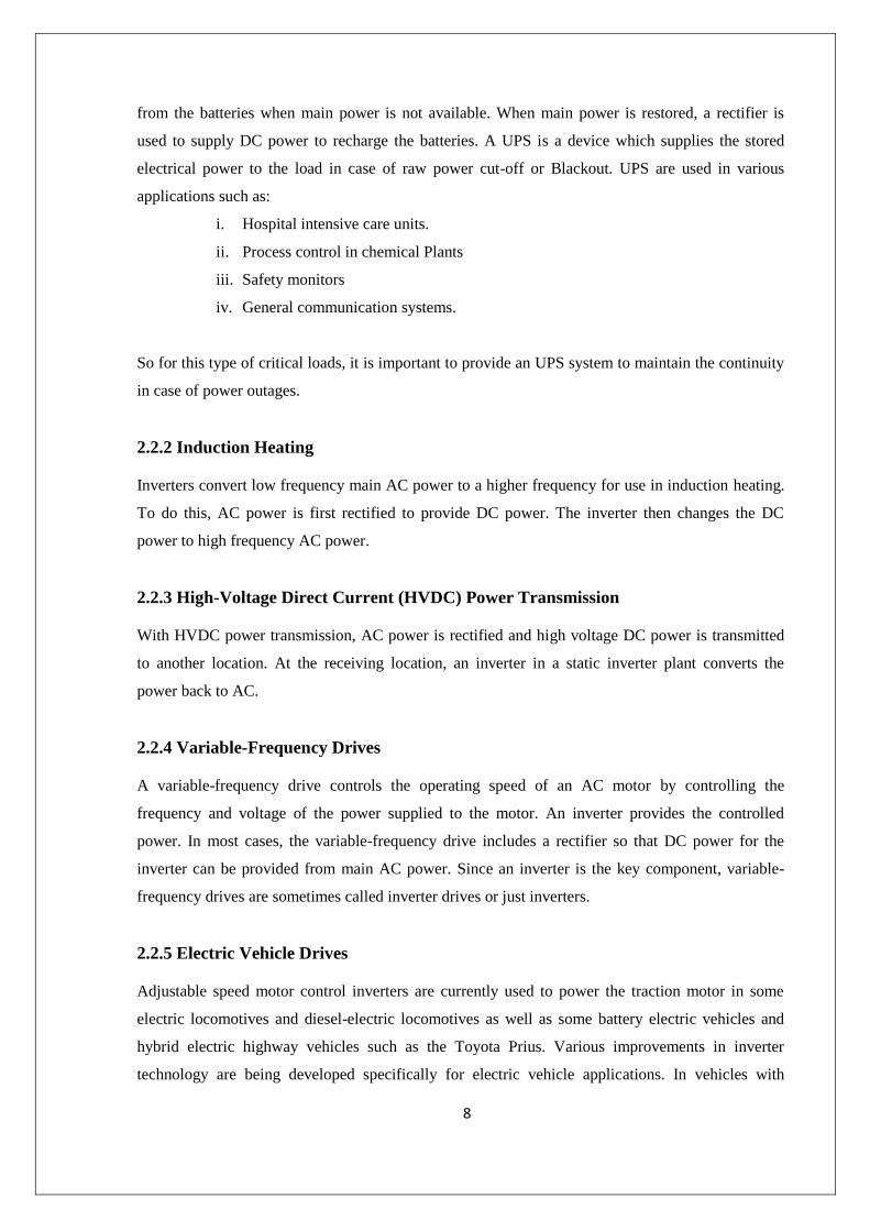
3.2 Square Wave Inverter
This is the basic type of inverter. Its output is an alternating square wave. In this inverter four
switches are operated at low frequency, and the output waveform is same as the switching
15
waveform with higher magnitude. The output is square wave and contain large number of lower
order harmonics. If the output frequency is 50Hz, the harmonic frequency is 150, 250, 350, 450 Hz
and so on. Therefore a large bulky filter is required at the output to get the sinusoidal output voltage.
The simple circuit diagram of a square wave inverter with generation of switching signal is shown
in Fig. 3.2. This type of inverter can run some household appliances without much problem but
unsuitable for complex and sensitive electronics equipment‟s [22].
Fig. 3.2: The circuit diagram of square wave inverter.
To designing the square wave inverter first we take two op-amp AD648C and then generate four
switching signal. The inverter circuit made of four switches. Now connect the switches with the
switching signal and take the output from load R1=100Ω. The generated output is a square wave.
The typical output waveshape of square wave inverter is shown in Fig. 3.3.
Fig. 3.3: The output wave shape of square wave inverter.
Figure 3.4 shows the frequency spectrum of the square wave inverter. This frequency response
curve shows the harmonics component from which we can calculate the value of THD.
16
(a)
(b)
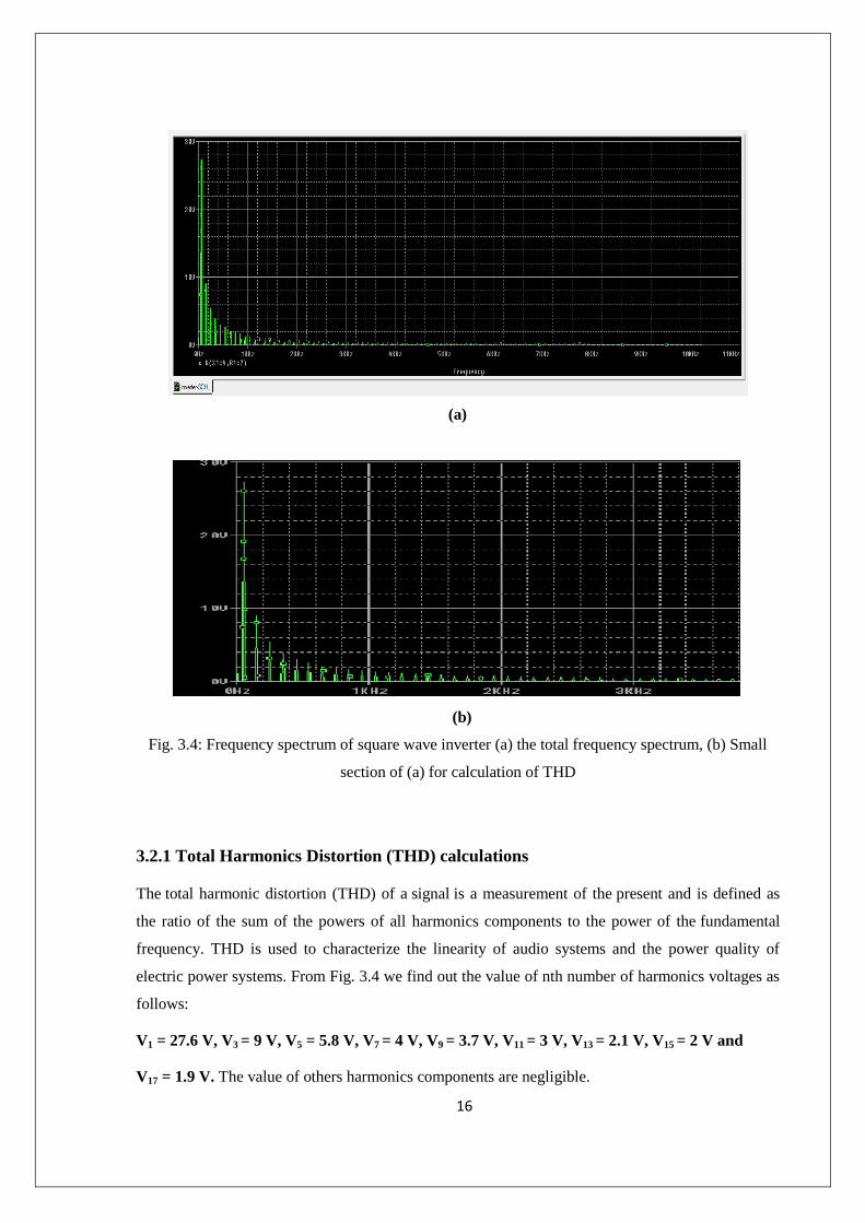
Fig. 3.4: Frequency spectrum of square wave inverter (a) the total frequency spectrum, (b) Small
section of (a) for calculation of THD
3.2.1 Total Harmonics Distortion (THD) calculations
The total harmonic distortion (THD) of a signal is a measurement of the present and is defined as
the ratio of the sum of the powers of all harmonics components to the power of the fundamental
frequency. THD is used to characterize the linearity of audio systems and the power quality of
electric power systems. From Fig. 3.4 we find out the value of nth number of harmonics voltages as
follows:
V1 = 27.6 V, V3 = 9 V, V5 = 5.8 V, V7 = 4 V, V9 = 3.7 V, V11 = 3 V, V13 = 2.1 V, V15 = 2 V and
V17 = 1.9 V. The value of others harmonics components are negligible.

17
Total Harmonics Distortion, THD = (V32+V5
2+V7
2+……………. +Vn
2)
1/2 /V1
= (9
2+5.8
2+4
2+3.7
2+3
2+2.1
2+2
2+1.9
2)
1/2/27.6
= 12.8588/27.6 = 0.4659
% of THD = 46.59%
In case of square wave inverter, THD is very high, nearly 47%, also the frequency of harmonic
components is very low, If the output frequency is 50Hz, the frequency of lowest order harmonic if
150Hz. Therefore, to get sinusoidal output voltage a low pass filter of cutoff frequency lower than
150Hz is required at the output. This type of low pass filter with very low cutoff frequency required
large size of inductor and capacitor, which is expensive and bulky. To overcome the problem of
large and bulky filter requirement is squire wave inverter, PWM technique is used.
3.3 PWM Inverter Design
The Pulse Width Modulation (PWM) is a technique which is characterized by the generation of
constant amplitude pulse by modulating the pulse duration. Analog PWM control requires the
generation of both reference and carrier signals that are feed into the comparator and based on some
logical output, the final output is generated. There are various types of PWM techniques and so we
get different output and the choice of the inverter depends on cost, noise and efficiency [23].
The DC-AC inverters usually operate on Pulse Width Modulation (PWM) technique. PWM
inverter is used to keep the output voltage of the inverter at the rated voltage (Depending on the
user‟s choice) irrespective of the output load. In a conventional inverter the output voltage changes
according to the changes in the load. Here we design a PWM inverter shows in Fig. 3.5 to nullify
this effect of the changing loads, the PWM inverter correct the output voltage by changing the width
of the pulses and the output AC depends on the switching frequency and pulse width which is
adjusted according to the value of the load connected at the output so as to provide constant rated
output. The inverters usually operate in a pulse width modulated (PWM) way and switch between
different circuit topologies, which means that the inverter is a nonlinear, specifically piecewise
smooth system. In addition to this, the control strategies used in the inverters are also similar to
those in DC-DC converters. The switching frequency of the PWM switching signal used in Fig. 3.5
is 4 kHz. The PWM switching signal is generated by comparing the sine wave with a high
frequency triangle wave using comparator circuit. Then PWM switching signals is used to operate
the switches of the inverter. The output of the PWM inverter is a high frequency PWM signal with
amplitude is equal to the input voltage of the power circuit. Figure 3.6 shows the typical waveform
of the PWM inverter. The output of the PWM inverter is a high frequency PWM signal with
amplitude is equal to the input voltage of the power circuit.

18
Fig. 3.5: The circuit diagram of PWM inverter.
3.3.1 Total Harmonics Distortion (THD) calculations
Total amount of distortion can be found from the frequency response curve. From the figure we
calculate the nth number of harmonics and find out % of THD. From the frequency spectrum, we
have calculated the value of the fundamental components and harmonics components. The values of
different components are found as follows:
V1 = 16 V, V2 = 5 V, V3 = 3.5 V, V4 = 1.9 V, V5 = 1.8 V, V6 = 1 V, the value of others harmonics
components are negligible.
THD = (V22+V3
2+V4
2+……………. +Vn
2)
1/2 /V1
=(52+3.5
2+1.9
2+1.8
2+1
2)
1/2/16 = 6.715/16 = 0.4197
THD=41.97%

19
(a)
(b)
Fig. 3.6: The frequency spectrum for PWM inverter (a) The total frequency spectrum, (b) small
section of (a) for calculation of THD.
In case of PWM inverter, THD is also high nearly 42%, however, the frequency of harmonics
components is very high, at switching frequency and it multiple. In this case the frequency of
triangular carrier wave is 4 kHz, consequently the frequency of switching signal is also 4 kHz.
Therefore, the frequency of lowest order harmonics is 4kHz, to filter out these harmonics
component we need to design a low pass filter with cutoff frequency very high around 4 kHz. This
type of low pass filter with high cutoff frequency is very easy to construct and required small size of
inductor and capacitor. In this case it is very easy to get pure sinusoidal output voltage with small
output filter which make the circuit small, more reliable and less expensive.

20
3.4 HSPWM Inverter Design
Power loss in a switching device comes from two sources. Every switching device has a resistive
element, so it dissipates power as current is conducted through the device. The resistive parameter is
described as on-resistance. These conduction losses are inversely proportional to the size of the
switching device. The other source of power loss is through switching losses. As the switching
device turn on and off, its intrinsic parasitic capacitance stores and then dissipates energy during
each switching transition. The switching losses are proportional to the switching frequency and the
values of the parasitic capacitances. As the physical size of the switching device increases, its
capacitance also increases; so, switching loss increasing. Therefore, using PWM technique, though
the quality of output wave can be improve, it significantly increase the switching loss. In Hybrid
PWM switching [5, 6] two of the four switches are driven at high switching frequency PWM signals
for high quality output and the other two are operated at low frequency usually at output frequency
to reduce the switching loss. This technique reduces the overall switching loss. Figure 3.7 shows the
circuit of HSPWM inverter. Figure 3.8 shows the circuit of HSPWM inverter with output filter.
Fig. 3.7: The circuit diagram of HSPWM inverter.
The output waveform of the HSPWM inverter is shown in Fig. 3.9. The output waveshapes of
HSPWM is the same as the output waveforms of PWM inverter as shown in Fig. 3.6. Therefore the
frequency spectrum of HSPWM, THD of HSPWM inverter will be the same as the PWM inverter.
A low pass LC filter is required at the output terminal to reduce harmonics generated by the output
waveform. While designing L-C filter, the cut-off frequency is chosen such that most of the low
order harmonics is eliminated. To operate as an ideal voltage source, that means no additional
voltage distortion even though under the load variation or a nonlinear load, the output impedance of
the inverter must be kept zero. Therefore, the capacitance value should be maximized and the

21
inductance value should be minimized at the selected cut-off frequency of the low-pass filter.
Fig. 3.8: The circuit diagram of HSPWM inverter with output filtering.
The output waveform of the HSPWM inverter after filter is shown in Fig. 3.9 and Fig. 3.10 shows
its frequency spectrum. Now to do the filtering add an output filter. The size of the filter parameters
are L=20mH and C=10uF.
Fig. 3.9: The output wave shape of HSPWM inverter after filtering.

22
Fig. 3.10: The frequency spectrum of output of HSPWM inverter after filtering.
Fig-3.10 shows that the output contains no harmonic component, output is pure sine wave. In
HSPWM inverter two of the four switches operates at high frequency and other two switches
operates at low frequency for all time. Therefore though total switching loss reduced in HPWM
switching technique, the switching losses of all switches are unequal. The switches driven with high
frequency switching signal dissipate more heat in comparison to the switches driven with low
frequency signals leading to unequal temperature rise at the switches. This reduces reliability of the
system. To overcome this drawback SHSPWM inverter is proposed in this thesis.
3.5 SHSPWM Inverter Design
The Symmetrical Hybrid Sinusoidal PWM inverter circuit will be design and analyze using ideal
switch and proper size of filter circuit. After this the ideal switch will be replaced by practical IGBT
switch.
3.5.1 STEP-1: PWM signal generation
PWM switching signal generation circuit is shown in Fig. 3.11. In this circuit the OPAMP acts as a
comparator, output of the OPAMP depends on the difference of the two inputs. In this circuit
positive input (saw-tooth wave) is kept fixed and negative input (sinusoidal voltage) is varied. The
outputs of OPAMP are used to on/off the switches of the power circuit. IC AD648C use as
opamp1. Inverter 74HC04 is connected with opamp1 through a resistorR101=1KΩ . Taking two
output signals from node 1. Both the output signals are shown in Fig. 3.12. From op-amp1 we get
PWM signals. Another output taking from IC74HC04 which is a PWM inverting signal. The
amplitude is 15V for both the signals

23
Fig. 3.11: PWM signal generation circuit.
(a)
(b)
Fig. 3.12: The output waveshape from IC AD648C (a) inverting output, (b) non-inverting output.
24
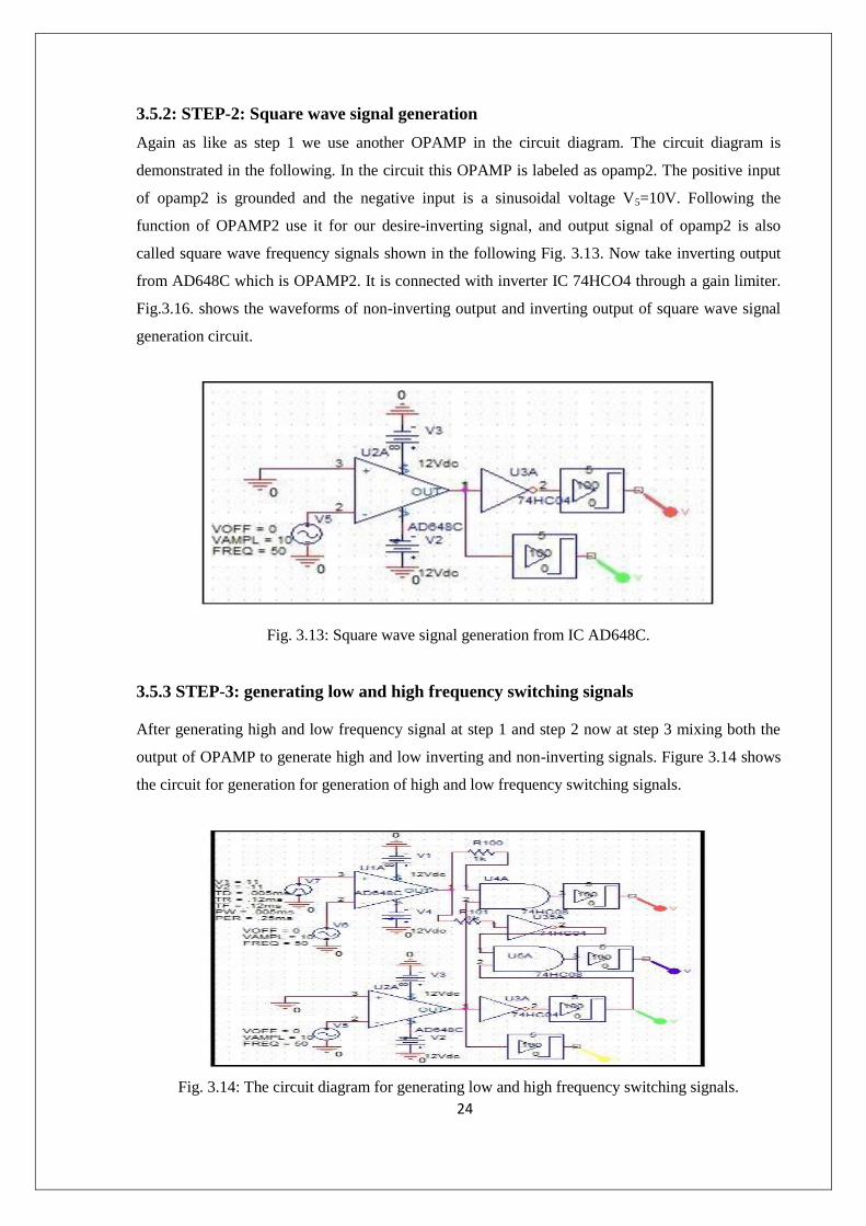
3.5.2: STEP-2: Square wave signal generation
Again as like as step 1 we use another OPAMP in the circuit diagram. The circuit diagram is
demonstrated in the following. In the circuit this OPAMP is labeled as opamp2. The positive input
of opamp2 is grounded and the negative input is a sinusoidal voltage V5=10V. Following the
function of OPAMP2 use it for our desire-inverting signal, and output signal of opamp2 is also
called square wave frequency signals shown in the following Fig. 3.13. Now take inverting output
from AD648C which is OPAMP2. It is connected with inverter IC 74HCO4 through a gain limiter.
Fig.3.16. shows the waveforms of non-inverting output and inverting output of square wave signal
generation circuit.
Fig. 3.13: Square wave signal generation from IC AD648C.
3.5.3 STEP-3: generating low and high frequency switching signals
After generating high and low frequency signal at step 1 and step 2 now at step 3 mixing both the
output of OPAMP to generate high and low inverting and non-inverting signals. Figure 3.14 shows
the circuit for generation for generation of high and low frequency switching signals.
Fig. 3.14: The circuit diagram for generating low and high frequency switching signals.

25
Opamp1 and op-amp 2 are connected with AND gate IC 74HC08. A truth table is a good way to
show the function of a logic gate. It shows the output states for every possible combination of input
states. The symbols 0 (false) and 1 (true) are usually used in truth tables.
The output becomes HIGH only when input A and input B are HIGH. In this circuit opamp1 which
present as U4A has two input. Point 1 is connected with OPAMP 1 through a resistor R 100=1K.Point
2 is connected with OPAMP 2. Another opamp2 which present as U5A also has two input. Point 1
is connected with OPAMP 1 through a inverter and resistor R 101=1K.Point 2 is connected with
OPAMP 2 through a inverter. The output waveform of low frequency switching signals and high
frequency switching signals are shown in Fig. 3.15 and Fig. 3.16.
(a)
(b)
Fig. 3.15: The output voltage waveform of (a) low frequency inverting signal, (b) low frequency
non-inverting signal.

26
(a)
(b)
Fig. 3.16: The output voltage waveform of (a) high frequency inverting signal, (b) high frequency
non-inverting signal.
Among the four signals two are high frequency switching signal and two are low frequency
switching signal. Both the high signals and low signals are inverting and non-inverting output
signal.
3.5.4: STEP-4: Generating high and low frequency signals together
The D Flip Flop is the most important of the Clocked Flip-flops Loading product data as it ensures
that inputs S and R are never equal to one at the same time. The D-type flip flops are constructed
from a gated SR flip-flop with an inverter added between the S and the R inputs to allow for a single
D (data) input [24].
The circuit diagram of D flip-flops is shown in Fig. 3.17.

27
Fig. 3.17: Circuit diagrams of D-flip flop.
Then this single data input, labelled D, is used in place of the “set” signal, and the inverter is used to
generate the complementary “reset” input thereby making a level-sensitive D-type flip-flop from a
level-sensitive RS-latch as now S = D and R = not D. The circuit for mixing low and high frequency
switching signals is shown in Fig. 3.18.
Fig. 3.18: The circuit for mixing low and high frequency switching signal together with the help of
flip-flop.
In this step use a D flip flop for mixing high and low frequency signals together. The input and
output waveforms of D flip-flops is shown in Fig. 3.19. In Fig. 3.192 the input clock pulse of the D-
flip flop denoted in green color. The output shows in red color taking from Q point of the D flip
flop. These ensure that the both inputs are never equal at the same time.

28
Fig. 3.19: The input and output waveform from flip-flop IC 74HC74.
3.5.5: STEP-5: generating four gate signals
A Logic OR Gate or Inclusive-OR gate is a type of digital logic gate that has an output which is
normally at logic level “0” and only goes “HIGH” to a logic level “1” when one or more of its
inputs are at logic level “1”. The output, Q of a “Logic OR Gate” only returns “LOW” again when
ALL of its inputs are at a logic level “0”. In other words for a logic OR gate, any “HIGH” input will
give a “HIGH”, logic level “1” output. The logic or Boolean expression given for a Digital Logic
OR Gate is that for Logical Addition which is denoted by a plus sign, ( + ) giving us the Boolean
expression of: A+B = Q. Then we can define the operation of a 2-input logic OR gate as being [25]
This is the most important part of the design. In this step four switching signals are generated. For
generating switching signals first high and low frequency signals are mixing together. To do so use
logic gates AND gate then OR gate. The circuit diagram for getting four switching signals (two of
high frequency and two are low frequency) is shown in Fig. 3.20.

29
Fig. 3.20: The circuit diagram for generating four gate signals.
In this step use four AND gate they are U8A,U9A U10A and U11A.U8A and U9A taking one input
from opamp2 which is a non-inverting low frequency signal.U10A and U11A taking one input from
opamp2 which is a inverting low frequency signal. Four AND gate taking another output from D
flip flops output Q. The low frequency signals coming from AND gates. Now to mixing high
frequency signals use four OR gate. OR gates are U12A,U13A,U14A and U15A has simultaneously
one input from AND gate U8A,U9A,U10A and U11A.U12A and U13A has another input from
opamp1 through AND gate U4A.which is a non-inverting high frequency signal. U14A and U15A
have another input from opamp1 through AND gate U5A.which is an inverting high frequency
signal.
3.5.6: STEP-6: Generating four gate signals using optocoupler
Opto-isolators, or Opto-couplers, are made up of a light emitting device, and a light sensitive
device, all wrapped up in one package, but with no electrical connection between the two, just a
beam of light. The light emitter is nearly always an LED. The light sensitive device may be a
photodiode, phototransistor, or more esoteric devices such as thyristors, triacs etc. A circuit diagram
of optocoupler and a typical output waveform is shown in Fig. 3.21.

30
(a)
b)
Fig. 3.21: a) A basic circuit diagram using optocoupler, b) typical output voltage waveforms of
optocoupler.
Optocoupler provides noise free isolated ground (IG). The primary reason for the use of isolated
grounds (IG) is to provide a noise-free ground return, separate from the equipment grounding (EG)
return. The EG circuit includes all of the metal conduit, outlet boxes, and metal enclosures that
contain the wiring and must be grounded to provide a safe return path in case of fault currents. The
circuit diagram for getting four switching signals using optocoupler is shown in Fig. 3.22.

31
Fig. 3.22: The circuit diagram for generating four gate signals using optocoupler.
The IG provides an insulated, separate ground path for the ground reference in electronic
equipment, such as computers, hospital equipment, and audio equipment. IG helps to eliminate the
potential for a ground loop, which can cause noise, data errors, and disruptions to these systems.
The IG is typically insulated and separate all the way back to the point of origin of the circuit, which
can be either a main panel or sub-panel [26]. The output waveforms of four optocoupler which is
the switching signal for four switches.
3.5.7: STEP-7: Designing SHSPWM Inverter
In this step-after generating four gate signals using optocoupler then generate the power circuit. The
power circuit consist of four switching device. As a switching device MOSFET is use. A power
MOSFET is a voltage controlled device and requires only a small input current, the switching speed
is very high and the switching times are of the order of nanoseconds. Power MOSFETs are finding
increasing applications in low power high frequency converters. MOSFETs do not have the
problems of second breakdown phenomena as do BJTs. However, MOSFETs have the problems of
electrostatic discharge and require special care in handling. In addition, it is relatively difficult to
protect them under short-circuited fault conditions. Some typical ratings for single MOSFETs are:

32
Table 3.1: Typical MOSFET ratings.
ID VDSS RDS
typical (max)
VGS (for ID ) VT
1A 900V 7 (9) 10V (0.5A) 1.5 - 3.5V
2A 500V 3 (4) 10V (1A) 2 - 4V
9A 200V 0.25 (0.4) 10V (5A) 2 - 4V
13A 500V 0.3 (0.4) 10V (7A) 2 - 4V
45 60V 0.024 (0.03) 10V (25A) 2 - 4V
Typical Switching Times
tON=td(on)+tr =delay+ rise time=18ns+25ns =43ns
tOFF=td(off)+tf =delay+ fall time=35ns+12ns =47ns
The circuit diagram of the proposed SHSPWM inverter without output filter is shown in Fig. 3.23.
Fig. 3.23: Final circuit diagram of the SHSPWM Inverter without filtering.
To design an Inverter, many power circuit topologies and voltage control methods are used. The
most important aspect of the Inverter technology is the output waveform. To filter the waveform
(Square wave, quasi sine wave or Sine wave) capacitors and inductors are used. Low pass filters, are

33
used to reduce the harmonic components. Resonant filter can be used if the Inverter has a fixed
output frequency. If the inverter has adjustable output frequency, the filter must be tuned to a level
above the maximum fundamental frequency. Feedback rectifiers are used to bleed the peak
inductive load current when the switch turns off. Table 3.2 summarizes the states of switches of the
inverter.
Table 3.2: Four state of the full bridge inverter.
State
Switches Closed
Vo
1 S1 & S2 + Vdc
2 S3 & S4 -Vdc
3 S1 & S3 0
4 S2 & S4 0
Figure3.27 shows that the switches S1 and S4 should not be closed at the same time. S2 and S3
should be closed in parallel too. Otherwise a short circuit would exist across the dc source. Real
switches do not turn on or off instantaneously. Hence, switching transition times must be
accommodated in the control of switches. Overlap of switch "on" will cause short circuit (shoot-
through fault) across the dc voltage source. The summary shows in the table 3.2.The time allowed
for switching is called blanking time [27]. Full bridge converter is also basic circuit to convert dc to
ac. An ac output is synthesized from a dc input by closing and opening switches in an appropriate
sequence. There are also four different states depending on which switches are closed. The output
wave shapes of SHSPWM are the same as the output waveforms of PWM and HSPWM inverter as
shown in Fig. 3.6. Consequently the frequency spectrum of HSPWM, THD of SHSPWM inverter
will be the same as the PWM inverter. Therefore the THD of SHSPWM inverter will be also nearly
42%.
Table 3.3: Comparison of different types of Inverter
Components Square wave
inverter
PWM Inverter HSPWM Inverter SHSPWM Inverter
THD 46.49 41.97 41.97 41.97
Filter Large bulky filter Small filer is
required
Very small filer is
required
Very small filer is
required
Switching
loss
Switching loss is
low
Switching loss is
increased
Switching loss of two
switches are high
Switching loss of all
four switches are equal

34
SHSPWM has been found efficient with lower switching loss and lower THD.
3.5.8: STEP-8: Filter Design for reducing harmonics:
This is the last step of our simulation. In this step for getting smooth sinusoidal output voltage, a
low pass LC filter of proper L and C value is needed at the output of this inverter. The block
diagram for design the output filter is shown in Fig. 3.24.
Fig. 3.24: Block diagram of an output filter design.
The Low pass filter is normally fitted at the inverter output to reduce the high frequency harmonics
components. The input to the filter is high frequency modulated 50 Hz ac input. The switching
signal that modulates the 50 Hz signal is taken to be 4 KHz in this case. So to make a filter that
would pass signal up to 1 KHz (say) and attenuate all other frequencies. This would result a nearly
sinusoidal output voltage. In the LC filter section we choose a capacitor of 100µF and determine the
value of inductor for a analysis through OrCAD simulation. Found the value of the inductor to be
200mH, which is the as used in case of design of HSPWM inverter. The proposed SHSPWM
inverter circuit with output filter is shown in Fig. 3.25. The output voltage of the proposed
SHSPWM inverter with output filter is shown in Fig. 3.26 and its frequency spectrum is shown in
Fig. 3.27. From Fig-3.27 it is found that the output contains no harmonic component, output is pure
sine wave.
LOAD =
DC SUPPLY INVERTER
LOW PASS FILTER
L
C

35
Fig. 3.25: Final circuit diagram of the SHSPWM Inverter after filtering the inverter.
Fig. 3.26: Output voltage wavefrom of the proposed SHSPWM inverter after filtering.

36
Fig. 3.27: The frequency spectrum of output of SHSPWM inverter after filtering.
3.6 Results
Square wave inverter: This is the basic type of inverter, in this inverter all the four switches are
operated at low frequency (power frequency). The output waveform of square wave inverter is
power frequency square wave, therefore contains a large number of lower order harmonics. To filter
a large bulky filter is required at the output. In this chapter firstly a square wave inverter is designed
and performance is analyzed. The percentage of THD of the square wave inverter is found nearly
47%.
Pulse Width Modulation (PWM) inverter: To overcome the problem of the requirement of the
large bulky filter at the output of the square wave inverter, PWM inverter is used. In PWM inverter
four snitches Sere operated at a frequency much higher than the power frequency. In case of PWM
technique the output of inverter contains fundamental components and harmonics components of
switching frequency and its multiple frequencies. The switching frequency is generally chosen at
kH range. To filter out these harmonics components at kH range is very easy and a very small filter
is required at the output to get the pure sinusoidal output voltage at the output. In PWM inverter
without filtering the percentage of THD is found nearly 42%. Due to high frequency switching of
all snitches the switching loss is high in this case.
Hybrid Sinusoidal Pulse Width Modulation (HSPWM) inverter: In PWM inverter all of the
four switches operated at high frequency causes higher switching loss, to overcome this drawbacks
HSPWM inverter is invented. In this technique out of four switches two are operated at high
frequency and two switches are operated at low frequency for all time. As a result the switching loss

37
becomes almost half. Switches operated at high frequency generate high heat as compared to the
switches operated at low frequency. Therefore, uniform heat is not generated in the circuit so the
reliability of the circuit is less. To overcome this drawbacks SHSPWM inverter is proposed in this
project. A HSPWM inverter is designed and performance is analyzes. The waveform of output
voltage and percentage of THD of HSPWM inverter is the same as the PWM inverter.
Symmetrical Hybrid Sine PWM Inverter (SHSPWM Inverter): In SHSPWM inverter, at any
time one switch operates at high frequency and one switch operate at low frequency. In this method
all switches operate at high frequency and low frequency alternatively. In this case the total
switching loss is equally distributed among the four switches which causes less heat generation and
equal heal generation. Therefore the reliability of the system is increased. The waveform of output
voltage and percentage of THD of SHSPWM inverter is the same as the PWM inverter.

38
Chapter-4
Implementation of SHSPWM Inverter
4.1 Experimental Setup
In this chapter the practical implementation of the SHSPWM Inverter is briefly discussed. After
getting the desirable result through ORCAD simulation the inverter circuit is practically
implemented in the laboratory. Figure 4.1 shows the picture of practically implemented inverter
circuit. Figure 4.2 shows the practically implemented inverter circuit under running condition
showing the SHSPWM switching signal.
The implemented inverter circuit can be divided into two parts, power circuit and control circuit.
The different components of the control circuit are shown in Fig. 4.3. The different components of
the power circuit of the practical implemented inverter circuit are shown in Fig. 4.4. In the control
circuit high frequency PWM signal is generated and low frequency snitching signal is generated.
Then logic circuit using flip-flop is used to generate the SHSPWM switching signals.
In this circuit four optocoupler are used for generating four isolated gate signal for driving the
IGBTs. But when optocoupler is connected at the output of the gate signal generating IC it is highly
loaded as a result the output voltage of the IC chip reduced to nearly zero which is insufficient to
drive the optocoupler. In order to reduce this loading effect a 4049B inverter IC is used. The lists of
the various elements used in the practically implemented circuit are given in Table-4.1 andTable-4.2
with brief description.

39
(a)
(b)
Fig. 4.1: Picture of practically implemented SHSPWM inverter (a) Final presentation of the circuit
b) Bread board arrangement.

40
Fig. 4.2: Picture of practically implemented SHSPWM inverter in working mode.
Fig. 4.3: Picture of the controlling circuit of implemented circuit showing its different components.
Fig. 4.4: Picture of the power circuit of implemented circuit showing its different components.

41
TABLE-4.1: List of the different components used in the control circuit of the practically
implemented inverter.
Sl.
No.
Name &
Model
Number
Quant
ity
Brief Description
1. IC L8038 2 The ICL8038 waveform generator is a monolithic integrated circuit capable
of producing high accuracy sine, square, triangular, sawtooth and pulse
waveforms with a minimum of external components. The frequency can be
selected externally from 0.001Hz to more than 300kHz using either resistors
or capacitors, and frequency modulation and sweeping can be accomplished
with an external voltage. The ICL8038 is fabricated with advanced
monolithic technology, using Schottky barrier diodes and thin film resistors,
and the output is stable over a wide range of temperature and supply
variations. These devices may be interfaced with phase locked loop circuitry
to reduce temperature drift to less than 250ppm/oC.
2. IC 741 2 The Operational Amplifier is probably the most versatile Integrated Circuit
available. It is very cheap especially keeping in mind the fact that it contains
several hundred components. The most common Op-Amp is the 741 and it is
used in many circuits. The OP AMP is a „Linear Amplifier‟ with an amazing
variety of uses. Its main purpose is to amplify (increase) a weak signal - a
little like a Darlington Pair. The OP-AMP has two inputs, INVERTING ( - )
and NON-INVERTING (+), and one output at pin 6.
3.
Optocoupler
4N25
4 The general purpose optocouplers consist of a gallium arsenide infrared
emitting diode driving a silicon phototransistor (NPN) in a 6-pin duel in-line
package. Rating: Collector emitter voltage = 30V, forward input current =
3A. LED power dissipation = 150 mW.
4.
IC
TL082CN
1 IC, OP AMP, DUAL JFET, DIP8; Op Amp Type: High Speed; No. of
Amplifiers:2; Bandwidth:3MHz; Slew Rate:16Vµs; Supply Voltage
Range:6V to 36V; Amplifier Case Style: DIP; No. of Pins:8; Operating
Temperature Range:0°C to +70°C; SVHC:No SVHC (20-Jun-2011);
Amplifier Type: JFET Operational; Base Number:082; Gain
Bandwidth:4MHz; IC Generic Number:082; IC Temperature Range:
Commercial; Input Offset Voltage Max:20mV; Logic Function Number:82;
Operating Temperature Max:70°C; Operating Temperature Min:0°C;

42
Package / Case: DIP; Slew Rate:16V/µs; Supply Voltage + Nom:15V;
Supply Voltage Max:36V; Supply Voltage Min:6V; Termination Type:
Through Hole
5.
IC
LH74LS04
1 7404 is a NOT gate IC. It consists of six inverters which perform logical
invert action. The output of an inverter is the complement of its input logic
state, i.e., when input is high its output is low and vice versa.
6. IC
HD 74LS08
1 In the 74LS series, the 74LS08 provides four 2-input AND gates. 74LS
series devices usually require a regulated 5 V power supply.
7.
IC 74HC112
1 HC112 and HCT112 utilize silicon-gate CMOS technology to achieve
operating speeds equivalent to LSTTL parts. They exhibit the low power
consumption of standard CMOS integrated circuits, together with the ability
to drive 10 LSTTL loads. These flip-flops have independent J, K, Set, Reset,
and Clock inputs and Q and Q\ outputs. They change state on the negative-
going transition of the clock pulse. Set and Reset are accomplished
asynchronously by low-level inputs.
The HCT logic family is functionally as well as pin-compatible with the
standard LS logic family.
8.
IC
SN74LS08
- The 74LS family (Low Power Schottky) of ICs is a lower-power version of
the 74S family.
9.
IC
SN74LS32
- These devices contain four independent 2-input OR gates. The SN5432,
SN54LS32 and SN54S32 are characterized for operation over the full
military range of -55°C to 125°C. The SN7432, SN74LS32 and SN74S32
are characterized for operation from 0°C to 70°C.
10. Resistance
10KΩ
Variable
2 -
11. Resistance
100KΩ
Variable
6 -
12. Resistance
4.7 KΩ
11 -
13. Resistance
18 KΩ
2 -
14. Resistance1 6 -

43
0KΩ
15. Resistance
100K Ω
4 -
16. Resistance 1
KΩ
4 -
17. Resistance
470Ω
4 -
18. Capacitor
4700µF
1 -
19. Capacitor
4.7nF
1 -
20. Capacitor
100nF
6 -
21. Capacitor
1000µF
1 -
22. Voltage
regulator
IC7805
1 7805 is a voltage regulator integrated circuit. It is a member of78xx series of
fixed linear voltage regulator ICs. The voltage source in a circuit may have
fluctuations and would not give the fixed voltage output. The voltage
regulator IC maintains the output voltage at a constant value. The xx in 78xx
indicates the fixed output voltage it is designed to provide. 7805 provides
+5V regulated power supply. Capacitors of suitable values can be connected
at input and output pins depending upon the respective voltage level.
TABLE-4.2: List of the different components used in the power circuit of the practically
implemented inverter.
Sl. No. Name & Model
Number
Quantity Brief Description
1. IC GT60N321 4 CH 600V 7.5A 3-Pin(3+Tab)
IGBT : tf = 0.25μ s (IC = 60 A) FRD: trr =
0.8μ s (di/dt = −20 A/μ s) Low saturation
voltage: VCE (sat) = 2.3V (typ.) (IC = 60 A)
2. Capacitor 1µF 1 A ceramic capacitor is a fixed value capacitor in
which ceramic material acts as the dielectric. It
is constructed of two or more alternating layers

44
of ceramic and a metal layer acting as the
electrodes. The composition of the ceramic
material defines the electrical behavior and
therefore applications.
3. Resistor 100 Ω 1 Ceramic Cement Power Resistor features good
heat resistant, low temperature coefficient, high
load power and high insulating capacity.
Widely used in computer, TV set, apparatus,
meter, sound and other equipment.
4. Inductor 2µH 1 -
5. Connecting port 13 -
4.2 Experimental Results
The switching frequency of the implemented circuit is choose to 4KHz.. IGBT IC GT60N321 used
as switches in the inverter circuit. A passive L-C filter is used in the circuit to attenuate the
switching harmonics from the output. Each gate signal is combined with High frequency PWM
signal and low frequency switching signals and vice versa. Figure 4.5 shows the waveform of
modulating sine wave of 50 Hz. Fig. 4.6 shows the waveform of the carrier wave of 4 kHz
frequency.
Fig. 4.5: Output sine voltage waveforms from IC L8038 sine wave generator, when input frequency
50KHz.

45
Fig.4.6: Output triangular voltage waveforms from IC L8038 triangular wave generator, when input
frequency 4KHz.
Figure 4.7 shows the waveform of the low frequency switching signal of frequency 50Hz and Fig.
4.8 shows the waveform of PWM signals.
Fig. 4.7: Output low frequency switching signal of frequency 50 Hz..
Fig. 4.8: Output PWM switching signal of frequency 4 kHz.

46
Fig. 4.9: Output High switching signal of frequency 4 kHz.
Fig. 4.10: Input and output voltage waveforms from flip flop IC 74HC112, when input frequency is
50Hz.
Figure 4.11 shows the waveforms of the SHSPWM switching signal which are the output of the
optocoupler and used for switching the switching devices (IGBTs).

47
(a)
(b)
(c)
(d)
Fig. 4.11: a)SHSPWM switching signal for (a) switch 1(IGBT-1), (b) switch 2(IGBT-2), (c) switch
3(IGBT-3), (d) switch 4(IGBT-4)
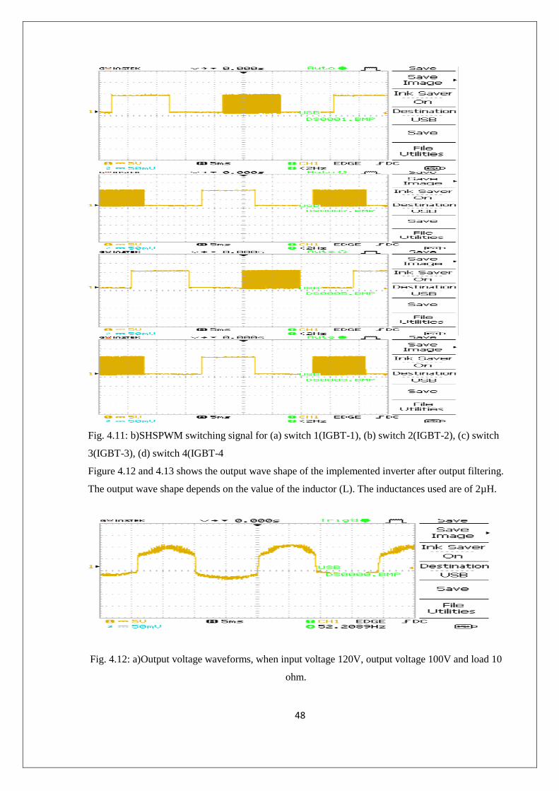
48
Fig. 4.11: b)SHSPWM switching signal for (a) switch 1(IGBT-1), (b) switch 2(IGBT-2), (c) switch
3(IGBT-3), (d) switch 4(IGBT-4
Figure 4.12 and 4.13 shows the output wave shape of the implemented inverter after output filtering.
The output wave shape depends on the value of the inductor (L). The inductances used are of 2µH.
Fig. 4.12: a)Output voltage waveforms, when input voltage 120V, output voltage 100V and load 10
ohm.

49
Fig. 4.12: b)Output voltage waveforms, when input voltage 120V, output voltage 100V and load
100 ohm.
Fig. 4.13: Output voltage waveforms across load from inverter circuit, when load is connected with
output filter at frequency 200Hz.
Table 4.3 summarizes the results of practically implemented inverter for load of 50Ω and Table 4.4
summarizes the results of practically implemented inverter for load of 100Ω . Table-4.5: summarizes
the result of the practically implemented inverter to find out the efficiency of the implemented
circuit when load is 200Ω . The efficiency of the circuit is near about 85 percent for input voltage of
around 30V. It is also clear the efficiency of the implemented circuit increases with the increases of
the input DC voltage.
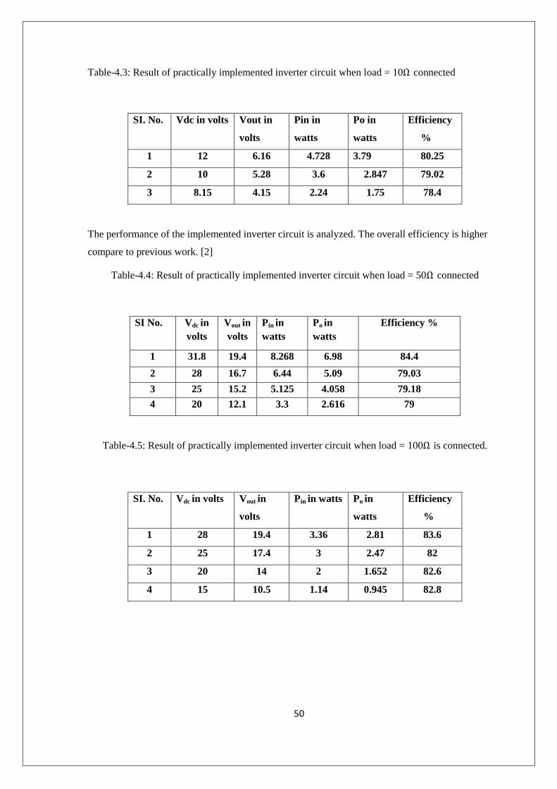
50
Table-4.3: Result of practically implemented inverter circuit when load = 10Ω connected
SI. No. Vdc in volts Vout in
volts
Pin in
watts
Po in
watts
Efficiency
%
1 12 6.16 4.728 3.79 80.25
2 10 5.28 3.6 2.847 79.02
3 8.15 4.15 2.24 1.75 78.4
The performance of the implemented inverter circuit is analyzed. The overall efficiency is higher
compare to previous work. [2]
Table-4.4: Result of practically implemented inverter circuit when load = 50Ω connected
SI No. Vdc in
volts
Vout in
volts
Pin in
watts
Po in
watts
Efficiency %
1 31.8 19.4 8.268 6.98 84.4
2 28 16.7 6.44 5.09 79.03
3 25 15.2 5.125 4.058 79.18
4 20 12.1 3.3 2.616 79
Table-4.5: Result of practically implemented inverter circuit when load = 100Ω is connected.
SI. No. Vdc in volts Vout in
volts
Pin in watts Po in
watts
Efficiency
%
1 28 19.4 3.36 2.81 83.6
2 25 17.4 3 2.47 82
3 20 14 2 1.652 82.6
4 15 10.5 1.14 0.945 82.8

51
Table-4.6: Result of practically implemented inverter circuit when load = 200Ω connected.
SI. No. Vdc in volts Vout in
volts
Pin in
watts
Po in
watts
Efficiency
%
1 31.8 24 2.835 2.4 84.6
2 28 21.9 2.24 1.917 85.58
3 25 17.2 1.95 1.62 83
4.3 Results
In this chapter the proposed SHSPWM inverter is implemented. Low frequency and high frequency
switching signal is generated using comparator circuit. Combination of logic circuits is used to
generate the SHSPWM switching signal from the high frequency and low frequency switching
signals. Simple JK flip-flop is used for generation of switching signal. In order to remove the
loading effect and to drive the IGBT, optocoupler is used. At the output stage of the proposed
inverter circuit a low pass filter is used to get the sinusoidal output voltage. However, the
parameters of the output filter are not found properly in the market. Hence the inductor of the filter
circuit is making by using ferrite core and the size of the inverter is much lower than the required
value. For that reason the output is found not pure sinusoidal however the percentage of THD after
filtering is less than 5%.
The performance of the implemented inverter circuit is analyzed. The output waveform of the
proposed inverter without filter is the same as the output waveform of PWM or HSPWM inverter,
therefore, the percentage of THD is the same as calculated for the PWM inverter or HSPWM
inverter in chapter 3 which was found around 42%. The efficiency of the implemented circuit is
calculated from input DC power and output AC power. The efficiency of the proposed inverter is
found around 85% for input DC voltage of around 30V which was found was around 76% in the
previous research. It is also clear that the efficiency of the circuit increases with the increases of the
input DC voltage. The effect of change of load resistance is also investigated, it is found that the
efficiency of the inverter circuit slightly increases with the increases of the load resistance.

52
Chapter-5
Conclusion and Recommendation
5.1 Conclusion
Bridge inverter consists of four switches which are operated by squire wave signal or by pulse width
modulated (PWM) high frequency switching signal. In square wave inverter, the switches are driven
by low frequency switching signals, result is large amount of low frequency harmonics in the
output. To reduce these harmonics a large filter is required.
In PWM techniques, all the four switches are operated by high frequency switching signals. In this
case the output consist harmonics of high frequency which is easy to filter. However, this technique
causes higher switching loss due to high frequency switching.
In hybrid PWM switching techniques two switches are operated by high frequency PWM switching
signals and other two switches are drive by low frequency switching signal signals for all times.
This technique reduces the overall switching loss to half but reduces reliability of the system due to
uneven heating of the switches. To overcome the drawback of uneven heating, a new switching
technique SHSPWM is proposed in this thesis. Starting from squire wave inverter a SHSPWM
inverter is designed step by step and in every case performance is analyzed in terms of THD and
output filter requirements. The percentage of THD of the square wave inverter is found nearly 47%,
whereas, the value of THD of the proposed inverter is nearly 42%. The requirement of output filter
of the proposed inverter is much lower than the square wave inverter. After simulation the proposed
SHSPWM inverter is implemented practically in the laboratory and performance is analyzed. In
practical circuit IGBT is used as switch to reduce the switching loss and JK flip-flop is used for its
simplicity. The efficiency of the implemented circuit is calculated from input DC power and output
AC power. The efficiency of the proposed inverter is found around 85% for DC input voltage of
around 30V which was around 76% in the previous research. The efficiency of the implemented
circuit will increase if the input DC voltage can be increases.

53
5.2 Recommendation for Future Work
In this thesis a SHSPWM inverter is designed and analyzed step by step starting from squire wave
inverter using simulation software. Finally the inverter is implemented in the laboratory and
performance of the inverter is analyzed in terms of THD and efficiency.
The switching loss in the switches is not calculated separately. Research can be done to determine
the switching loss of the switching devices and design of proper switching frequency to reduce the
overall switching loss.
In this project the SHSPWM switching signals are generated using comparator and logic gates.
Research can be done to generate the SHSPWM switching signal using microcontroller.

54
REFERENCES
[1] N. Mohan, T. M. Underland and W. P. Robbins, “Power Electronics: Converter, Applications
and Design”, John Wiley and Sons, pp. 211-218, 2003.
[2 ] Ramprasad Panda, R.K. Tripathi „A symmetrical hybrid sine PWM switching technique for full
bridge inverters ‟India International Conference on power electronics Pages: 345 -348,2006
[3] Wei Kekan, Trillion Q . Zheng, Ran Wang, and Chenchen wang ‘Study on Hybrid PWM Method
under Low Switching Frequency’ Journal of International Conference on Electrical Machines
and Systems Vol. 1, No.2 , pp.205~ 210 , 2012 205
[4] Holt and Mike, “The Basics of Isolated Grounding Receptacles”, EC& M, retrieved 25 March
2011.
[5] M. H. Rahsid, “Power Electronics Handbook: Devices, Circuits, and Applications”, Elsevier.
pp. 147–564.
[6] Baker RH, “High-voltage converter circuit”, US Patent 4-203-151, May 1980.
[7] http:// www.studer-inno.com
[8] P.N. Enjeti, P. D. Ziogas and J. F. Lindsay, “Programmed PWM techniques to eliminate
harmonics: A critical evaluation”, IEEE transactions on Industrial Applications, vol. 26, no. 2,
pp. 302-316, April 1990.
[9] P .K.Banerjee and, K. Raahemifar, “AC-AC Voltage Regulation by Switch mode PWM Voltage
Controller with Improved performance”, International Journal of Engineering Research and
Technology”.vol. 2, Issue 9,e-ISSN 2278-0181.
[10] M. R. Hasan, M. A. H. Sadi, I. Al-Baqee, M. S. I. Bhuiyan and M. K. Hossain, “A Proposed
Development of Dc-Dc Transformer using CUK regulator”,. International Journal of
Engineering and Technology.Vol3,N0-4-August 2011.
[11] A. Kumar and R. Gupta, “Single–phase AC/DC/AC converter using inverter”, Power, In
Proceeding of International Conference on Control and Embedded Systems (ICPCES), 2010,
pp. 1-5, 2010.
[12] G. Kassakian , M.F. Schlecht and G.C. Vergese, Principles of Power Electronics, Addison-
Wesley Publishing Company
[13] Owen, Edward L. , “Origins of the Inverter”. IEEE Industry Applications Magazine: History
Department (IEEE) VOL 2 (1), PP 64-66. January-February 1996.
[14] S. Yang, F. Z. Peng, Q. Lei, R. Inoshita and Z. Qian, “Current-fed quasi-Z-source inverter with

55
voltage buck-boost and regeneration capability,” Proceedings of IEEE ECCCE‟09, pp. 3675-
3682, Sept. 2009.
[15] S.B. Kjaer, J.K. Pederson, F. Blaabjerg, “Power inverter topologies for photovoltaic modules-a
review”, IEEE proc. of 37th annual industry application conference (IAS‟02), vol. 2, pp.782-
788, 2002.
[16] ) URL:http://imtiazhussainkalwar.weebly.com
[17] OrCAD Software, Release 9: 1985-1999 OrCAD, Inc., U.S.A
[18] www.ee.surrey.ac.uk/Projects/CAL/digital-logic/gatesfunc
[19] www.electronics-tutorials.ws › Sequential Logic
[20] www.ee.surrey.ac.uk/Projects/CAL/digital-logic/gatesfunc
[21] www.powere.dynamictopway.com
[22] imtiazhussainkalwar.weebly.Com(feedback control systems-by–dr imtiaz hussain)
[23]G.Kennedy, Electronic Communication System(3rd
ed.).New York:McGraw-Hill
Book Reference
• Power Electronics Circuits, Devices, and Applications.
_Muhammad H.Rashid
• Theory of Power Electronics
_K. L. Rao
_CH. Saibabu
Spice for Power Electronics and Electronic Power
_Muhammad H. Rashid
_Hasan M. Rashid
Pspice And Circuit Analysis
_John. Keown
Switchgear Protection And Power System protection.
_ Sunil S. Rao
Electronic Communication System _ G.Kennedy