Embed Size (px)
Citation preview
1
A R E P O R T
ON
DESIGN OF 16 – BIT RISC PROCESSOR
Under the guidance ofDr. Chandra Shekhar, Director, CEERI, Pilani.
By
Raj Kumar Singh Parihar 2002A3PS013Shivananda Reddy 2002A3PS107
BIRLA INSTITUTE OF TECHNOLOGY AND SCIENCEPILANI – 333031
May 2006
2
A R E P O R T
ON
DESIGN OF 16 – BIT RISC PROCESSOR
Under the guidance of
Dr. Chandra Shekhar, Director, CEERI, Pilani.
By
Raj Kumar Singh Parihar 2002A3PS013Shivananda Reddy 2002A3PS107
B.E. (Hons) Electrical and Electronics Engineering
Towards the partial fulfillment of the course BITS C335,Computer Oriented Project
BIRLA INSTITUTE OF TECHNOLOGY AND SCIENCEPILANI – 333031
May 2006

3
ACKNOWLEDGEMENTS
We are very thankful Dr. Chandra Shakhar, Director, CEERI – Pilani for giving us an
opportunity to work under her guidance. The love and faith that she showered on us
helped us to go on and complete the project successfully.
We would like to extend our sincere thank to Dr. Anu Gupta, EEE, BITS - Pilani for
their valuable suggestions and guidance, Mr. Pawan Sharma, In-charge OLAB for their
support, Mr. Ninad Kothari, TA, BITS - Pilani for Encouragement.
Last but not the least we would like to thank our Friends, Parents, Family members and
invisible force which provided moral support and spiritual strength, which helped us
completing the work successfully.

4
BIRLA INSTITUTE OF TECHNOLOGY AND SCIENCE
PILANI (Rajasthan) – 333031
CERTIFICATE
This is to certify that the project entitled “Design of 16 bit RISC Processor”
is the bonafide work of Shivananda Reddy (2002A3PS107) done in the
second semester of the academic year 2005-2006. He has duly completed his
project and has fulfilled all the requirements of the course BITS C335,
Computer Laboratory Oriented Project, to my satisfaction.
Dr. Chandra Shekhar
Director, CEERI, Pilani
Date:
5
BIRLA INSTITUTE OF TECHNOLOGY AND SCIENCE
PILANI (Rajasthan) – 333031
CERTIFICATE
This is to certify that the project entitled “Design of 16 bit RISC Processor”
is the bonafide work of Raj Kumar Singh Parihar (2002A3PS013) done in
the second semester of the academic year 2005-2006. He has duly completed
his project and has fulfilled all the requirements of the course BITS C335,
Computer Laboratory Oriented Project, to my satisfaction.
Dr. Chandra Shekhar
Director, CEERI, Pilani
Date:
6
ABSTRACT
This project includes the designing of 16-Bit RISC processor and modeling of its
components using Verilog HDL. The implementation strategies have been
borrowed from most popular DLX and MIPS architecture up to certain extent.
The instruction set adopted here is extremely simple that gives an insight into the
kind of hardware which should be able to execute the set of instructions properly.
Along with sequential and combinational building blocks of NON- pipelined
processor such as adders and registers more complex blocks i.e. ALU and
Memories had been designed and simulated. The modeling of ALU which has
been done in this project is fully structural starting from half adders. At the end
the semi custom layout had been developed for ALU using AMI05 Technology
and IC station tool. Complex blocks have been modeled using behavioral
approach i.e. Memories, whereas simple blocks i.e. Adders had been done through
structural approach. The tools which had been used throughout the project work
are Modelsim (Digital Simulation), Leonardo Spectrum (Digital synthesis) and
IC station (Digital Semi custom Layout). For synthesis purpose the targeted
FPGA device technology was ALTERA, Cyclone, and EP1C6Q240C. A simple
sequential block’s performance and figure of merits were observed under the
constraints clock frequency: 50 MHz and DRT: 5ns.
7
TABLE OF CONTENTS
ACKNOWLEDGEMENT .......................................................................... 3
CERTIFICATE .................................................................Error! Bookmark not defined.
ABSTRACT.................................................................................................. 6
1. CEERI: An Introduction ........................................................................ 8
2. RISC : An introduction ........................................................................... 9
3. RISC vs CISC ......................................................................................... 11
3.1 CISC Designs ......................................................................................................... 11
3.2 The bridge toward RISC (Historical factors) ......................................................... 11
3.3 Why RISC? ............................................................................................................ 12
4. RISC: Top level Description and guidelines ........ Error! Bookmark not defined.
4.1 Instruction Set Architecture .....................................Error! Bookmark not defined.
4.2 Microarchitecture ....................................................Error! Bookmark not defined.
5. Design and Simulation: Building Blocks ............................................. 23
5.1 Sequential Element: D- Flip Flop .......................................................................... 23
5.2 Combinational Element: N-Bit add-subtract Module ............................................ 27
6. ASIC Design Flow: Design of a 16-Bit ALU ....................................... 33
7. Implementation: 16-Bit Non-pipelined RISC Processor ................... 44
Appendix-I II III .......................................................................................... 63
Bibliography ................................................................................................ 82
8
1. CEERI: An Introduction
Central Electronics engineering Research Institute, popularly known as CEERI, is
a constituent establishment of the Council of Scientific and Industrial Research (CSIR),
New Delhi. The foundation stone of the institute was laid on September 21, 1953 by the
then Prime Minister of India, Pt. Jawaharlal Nehru. The actual R&D work started toward
the end of 1958. The institute has blossomed into a center for excellence for the
development of technology and for advanced research in electronics. Over the years the
institute has developed a number of products and processes and has established facilities
to meet the emerging needs of electronics industry.
CEERI, Pilani, since its inception, has been working for the growth of electronics in
the country and has established the required infrastructure and intellectual man power for
undertaking R&D in the following three major areas:
1) Semiconductor Devices
2) Microwave Tubes
3) Electronics Systems
The activities of microwave tubes and semiconductor devices areas are done at Pilani
whereas the activities of electronic systems area are undertaken at Pilani as well as the
two other centers at Delhi and Chennai. The institute has excellent computing facilities
with many Pentium computers and SUN/DEC workstations interlined with internet and e-
mail facilities via VSAT. The institute has well maintained library with an outstanding
collection of books and current journals (and periodicals) published all over the world.
CEERI, with its over 700 highly skilled and dedicated staff members, well-equipped
laboratories and supporting infrastructure is ever enthusiastic to take up the challenging
tasks of research and development in various areas.
9
2. RISC: An Introduction
The reduced instruction set computer, or RISC, is a microprocessor CPU
design philosophy that favors a smaller and simpler set of instructions that all take about
the same amount of time to execute. The most common RISC microprocessors are ARM,
DEC Alpha, PA-RISC, SPARC, MIPS, and IBM's PowerPC.
The idea was inspired by the discovery that many of the features that were
included in traditional CPU designs to facilitate coding were being ignored by the
programs that were running on them. Also these more complex features took several
processor cycles to be performed. Additionally, the performance gap between the
processor and main memory was increasing. This led to a number of techniques to
streamline processing within the CPU, while at the same time attempting to reduce the
total number of memory accesses.
When the controller design become more complex in CISC and the performance
was also not up to expectations, people started looking on some other alternatives. It had
been found that when a processor talks to the memory the speed gets killed. So the one
improvement on CPI was to keep the instruction set very simple. Simple in not the way it
works but the way it looks. That’s why we have very few instructions in any typical
RISC architecture where processor asks data from memory probably not other than Load
and Store. We avoid keeping such addressing modes. The complexity of controller design
has been overcome with the help of operands and Opcode bits fixed in instruction
register. At the end the pipelining added a new dimension in the speed just with the help
of some additional registers. Now what pipeline does is it increases throughput by
reducing CPI. The instruction can be executed effectively in one clock cycle. The
pipelining in any kind of architecture took birth from the inherent parallelism and the idle
states of components.
The pipelined architecture could be further enhanced with the concepts known as
super-scaling. There we provide more than one execution unit. The time when one unit is
10
busy with the current execution task, the fetch unit can probably fetch he next instruction
which would be executed with the help of some other execution unit present in system.
Features which are generally found in RISC designs are:
uniform instruction encoding (for example the op-code is always in the same bit
position in each instruction, which is always one word long), which allows faster
decoding;
A homogeneous register set, allowing any register to be used in any context and
simplifying compiler design.
simple addressing modes (complex addressing modes are replaced by sequences
of simple arithmetic instructions);
Few data types supported in hardware (for example, some CISC machines had
instructions for dealing with byte strings. Others had support for polynomials and
complex numbers. Such instructions are unlikely to be found on a RISC machine).
Over many years, RISC instruction sets have tended to grow in size. Thus, some have
started using the term "load-store" to describe RISC processors, since this is the key
element of all such designs. Instead of the CPU itself handling many addressing modes,
load-store architecture uses a separate unit dedicated to handling very simple forms of
load and store operations. CISC processors are then termed "register-memory" or
"memory-memory".
Today RISC CPUs (and microcontrollers) represent the vast majority of all CPUs in
use. The RISC design technique offers power in even small sizes, and thus has come to
completely dominate the market for low-power "embedded" CPUs. Embedded CPUs are
by far the largest market for processors. RISC had also completely taken over the market
for larger workstations for much of the 90s. After the release of the Sun SPARCstation
the other vendors rushed to compete with RISC based solutions of their own. Even the
mainframe world is now completely RISC based.
11
3. RISC vs CISC
3.1 CISC DesignsAn overriding characteristic of CISC machines is an approach to instruction set
architecture that emphasizes doing more with each instruction. As a result, CISC
machines have a wide variety of addressing modes. CISC machines take a “have it your
way” approach to the location and number of operands in various instructions. As a result
instructions are of widely varying length and execution times.
3.2 The bridge toward RISC (Historical factors)The capabilities of CISC allowed more operations to be performed into the same
program size. During that period, program and data storage were given more importance
since cost of memory was high.
An attempt was made to narrow the semantic gap, that is, the gap that existed
between machine instruction sets and high level language constructs with complicated
instructions and addressing modes to obtain performance increase. Most of these
“improvements” were rejected by compiler writers on the context that they did not fit
well with the language requirements and were of only limited usefulness. At the same
time, research conducted by David Patterson and Donald Knuth showed that 85% of a
program’s statements were assignments, conditional or procedure calls. Nearly 80% of
the assignment statements were MOVE instructions with no arithmetic operations.
As more and more capabilities were added to the processors, it was found
increasingly difficult to support higher clock speeds that would otherwise have been
possible. Complex instructions and addressing modes worked against higher clock
speeds, because of the greater number of microscopic actions that had to be performed
per instruction. Moreover, RAM prices dropped sufficiently so that the pressure on
system designers was less to design instructions that did more that it was to design
systems that were faster. It was also becoming cost-effective to employ small amounts of
higher-speed cache memory to reduce memory latency i.e. the writing time between
when a memory is made and when it has been satisfied.
12
3.3 Why RISC?Various attempts have been made to increase the instruction execution rates by
overlapping the execution of more than one instruction since the earliest day of
computing. The most common ways of overlapping are pre-fetching, pipelining and
superscalar operation.
1) Pre-fetching: The process of fetching next instruction or instructions into an
event queue before the current instruction is complete is called pre-fetching. The
earliest 16-bit microprocessor, the Intel 8086/8, pre-fetches into a non-board
queue up to six bytes following the byte currently being executed thereby making
them immediately available for decoding and execution, without latency.
2) Pipelining: Pipelining instructions means starting or issuing an instruction prior
to the completion of the currently executing one. The current generation of
machines carries this to a considerable extent. The PowerPC 601 has 20 separate
pipeline stages in which various portions of various instructions are executing
simultaneously.
3) Superscalar operation: Superscalar operation refers to a processor that can issue
more than one instruction simultaneously. The PPC 601 has independent integer,
floating-point and branch units, each of which can be executing an instruction
simultaneously.
CISC machine designers incorporated pre-fetching, pipelining and superscalar operation
in their designs but with instructions that were long and complex and operand access
depending on complex address arithmetic, it was difficult to make efficient use of these
new speed-up techniques. Furthermore, complex instructions and addressing modes hold
down clock speed compared to simple instructions. RISC machines were designed to
efficiently exploit the caching, pre-fetching, pipelining and superscalar methods that were
invented in the days of CISC machines.
13
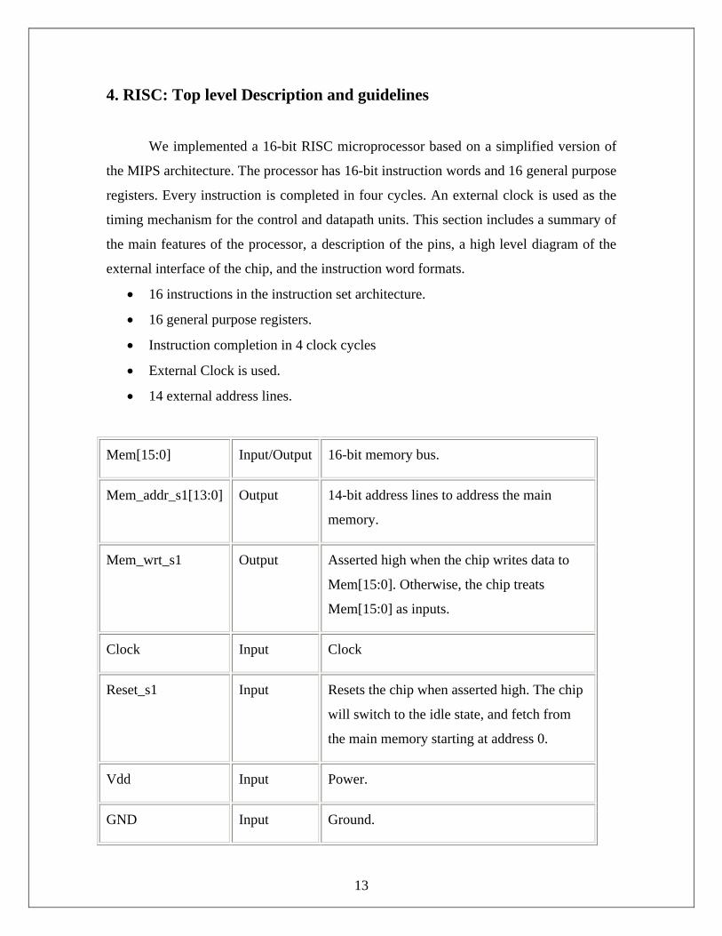
4. RISC: Top level Description and guidelines
We implemented a 16-bit RISC microprocessor based on a simplified version of
the MIPS architecture. The processor has 16-bit instruction words and 16 general purpose
registers. Every instruction is completed in four cycles. An external clock is used as the
timing mechanism for the control and datapath units. This section includes a summary of
the main features of the processor, a description of the pins, a high level diagram of the
external interface of the chip, and the instruction word formats.
16 instructions in the instruction set architecture.
16 general purpose registers.
Instruction completion in 4 clock cycles
External Clock is used.
14 external address lines.
Mem[15:0] Input/Output 16-bit memory bus.
Mem_addr_s1[13:0] Output 14-bit address lines to address the main
memory.
Mem_wrt_s1 Output Asserted high when the chip writes data to
Mem[15:0]. Otherwise, the chip treats
Mem[15:0] as inputs.
Clock Input Clock
Reset_s1 Input Resets the chip when asserted high. The chip
will switch to the idle state, and fetch from
the main memory starting at address 0.
Vdd Input Power.
GND Input Ground.
14
Fig.4 High Level Block Diagram that describes the external interface of the chip
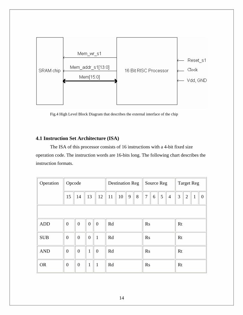
4.1 Instruction Set Architecture (ISA)
The ISA of this processor consists of 16 instructions with a 4-bit fixed size
operation code. The instruction words are 16-bits long. The following chart describes the
instruction formats.
Opcode Destination Reg Source Reg Target RegOperation
15 14 13 12 11 10 9 8 7 6 5 4 3 2 1 0
ADD 0 0 0 0 Rd Rs Rt
SUB 0 0 0 1 Rd Rs Rt
AND 0 0 1 0 Rd Rs Rt
OR 0 0 1 1 Rd Rs Rt
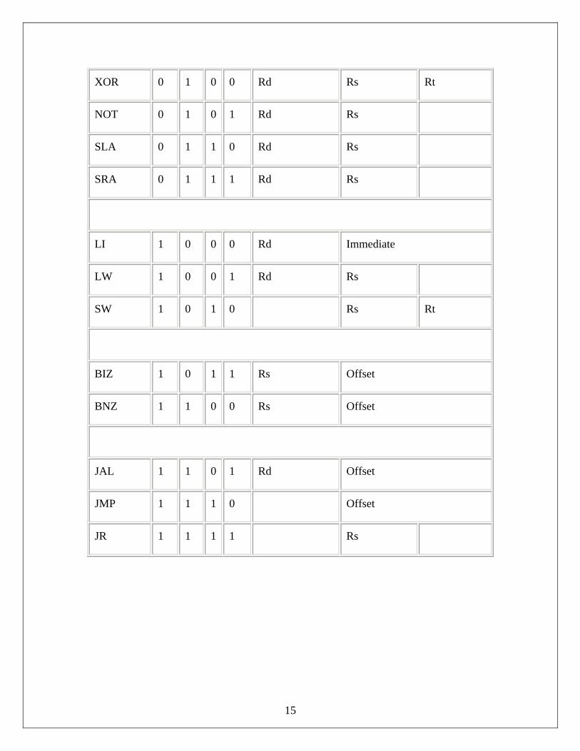
15
XOR 0 1 0 0 Rd Rs Rt
NOT 0 1 0 1 Rd Rs
SLA 0 1 1 0 Rd Rs
SRA 0 1 1 1 Rd Rs
LI 1 0 0 0 Rd Immediate
LW 1 0 0 1 Rd Rs
SW 1 0 1 0 Rs Rt
BIZ 1 0 1 1 Rs Offset
BNZ 1 1 0 0 Rs Offset
JAL 1 1 0 1 Rd Offset
JMP 1 1 1 0 Offset
JR 1 1 1 1 Rs
16
The Processor features five instruction classes:
1. Arithmetic (Two’s Complement) ALU operation (2)
ADD: Rd = Rs + Rt
Operands A and B stored in register locations Rs and Rt are added and written to the
destination register specified by Rd.
SUB: Rd = Rs - Rt
Operand B (Rt) is subtracted from Operand A (Rs) and written to Rd.
2. Logical ALU operation (6)
AND: Rd = Rs & Rt
Operand A (Rs) is bitwise anded with Operand B (Rt) and written into Rd.
OR: Rd = Rs | Rt
Operand A (Rs) is bitwise ored with Operand B (Rt) and written into Rd.
XOR: Rd = Rs ^ Rt
Operand A (Rs) is bitwise Xored with Operand B (Rt) and written into Rd.
NOT: Rd = ~Rs
Operand A (Rs) is bitwise inverted and written into Rd.
SLA: Rd = Rs << 1
Operand A (Rs) is arithmetically shifted to the left by one bit and written into Rd.
SRA: Rd = Rs >> 1
Operand A (Rs) is arithmetically shifted to the right by one bit and written into Rd. The
MSB (sign bit) will be preserved for this operation.
3. Memory operations (3)
LI: Rd = 8-bit Sign extended Immediate
The 8-bit immediate in the Instruction word is sign-extended to 16-bits and written into
the register specified by Rd.
LW: Rd = Mem[Rs]
17
The memory word specified by the address in register Rs is loaded into register Rd.
SW: Mem[Rs] = Rt
The data in register Rt is stored into the memory location specified by Rs.
4. Conditional Branch operations (2)
BIZ: PC = PC + 1 + Offset if Rs = 0
If all the bits in register Rs are zero than the current Program Count (PC + 1) is offset to
PC + 1 + Offset. The count is offset from PC + 1 because it is incremented and stored
during the Fetch cycle.
BNZ: PC = PC + 1 + Offset if Rs! = 0
If all the bits in register Rs are not zero than the current Program Count (PC + 1) is offset
to PC + 1 + Offset.
5. Program Count Jump operations (3)
JAL: Rd = PC + 1 and PC = PC + 1 + Offset
Jump and Link instruction would write current Program Count in register Rd and offset
the program count to PC + 1 + Offset
JMP: PC = PC + 1 + Offset
Unconditional jump instruction will offset the program count to PC + 1 + Offset.
JR: PC = Rs
Jump Return instruction will set the Program Count to the one previously stored in JAL.
FETCH INSTRUCTION
Part 1
Retrieve instruction word from main memory
Increment Program Counter and store in ALU Out
Part 2
Write Incremented Program Count
Load Operands into latches from Register File
18
EXECUTE INSTRUCTION
Part 1
Perform ALU Operation based instruction word and store in ALU Out
Move Memory Word into MDR for Load Word operation
Write Data into Memory from Register File for Store Word operation
Part 2
Write ALU, IR (Immediate), or MDR data into Register File
Write new Program Count for Jump Operation or it Branch taken
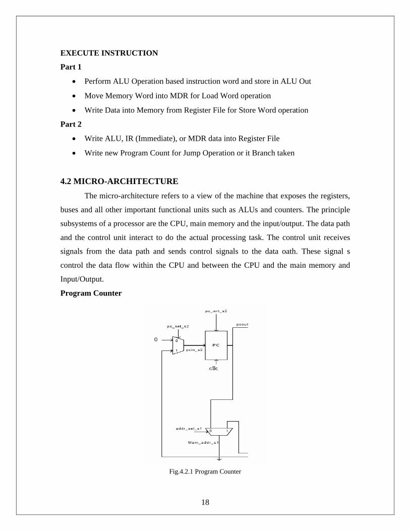
4.2 MICRO-ARCHITECTURE
The micro-architecture refers to a view of the machine that exposes the registers,
buses and all other important functional units such as ALUs and counters. The principle
subsystems of a processor are the CPU, main memory and the input/output. The data path
and the control unit interact to do the actual processing task. The control unit receives
signals from the data path and sends control signals to the data oath. These signal s
control the data flow within the CPU and between the CPU and the main memory and
Input/Output.
Program Counter
Fig.4.2.1 Program Counter
19
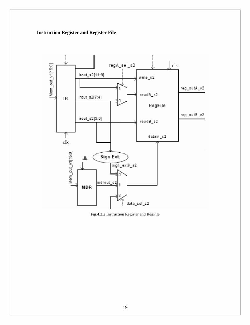
Instruction Register and Register File
Fig.4.2.2 Instruction Register and RegFile
20
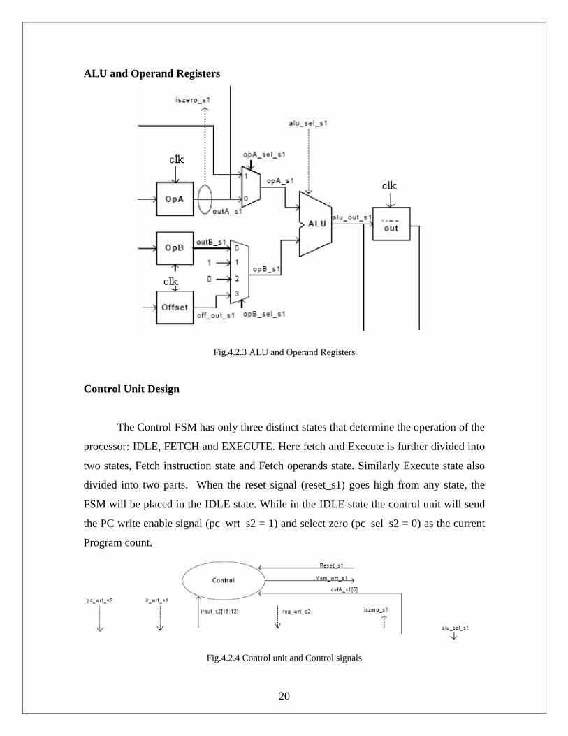
ALU and Operand Registers
Fig.4.2.3 ALU and Operand Registers
Control Unit Design
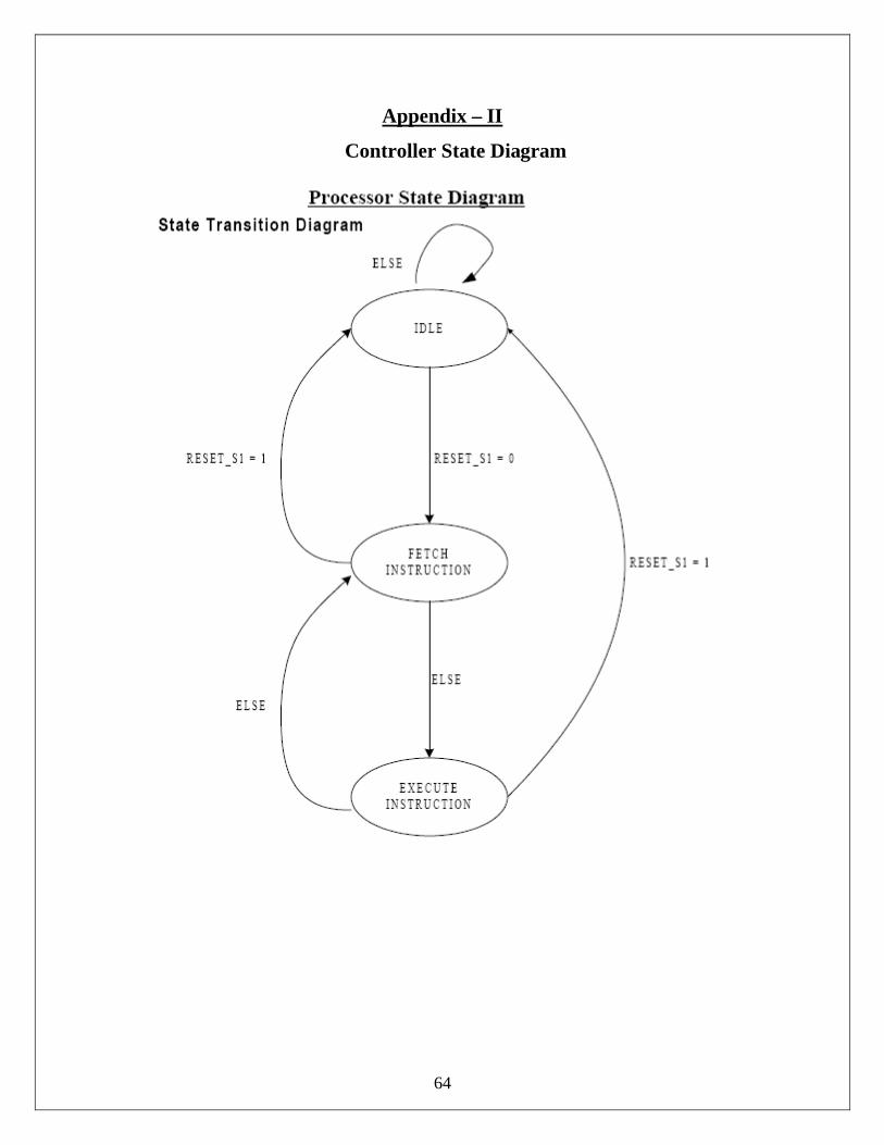
The Control FSM has only three distinct states that determine the operation of the
processor: IDLE, FETCH and EXECUTE. Here fetch and Execute is further divided into
two states, Fetch instruction state and Fetch operands state. Similarly Execute state also
divided into two parts. When the reset signal (reset_s1) goes high from any state, the
FSM will be placed in the IDLE state. While in the IDLE state the control unit will send
the PC write enable signal (pc_wrt_s2 = 1) and select zero (pc_sel_s2 = 0) as the current
Program count.
Fig.4.2.4 Control unit and Control signals
21
When the reset signal goes low, the FSM’s next state will be the FETCH state and
the instruction from Memory address 0 will be loaded into the Instruction Register (IR) to
begin program execution. The control looks at the next state = FETCH and generates the
IR write (ir_wrt_s1), Operand A Select (opA_sel_s1), Operand B Select (opB_sel_s1 =
0010) and the ALU add operation (alu_op_s1 = 00000001) to load the IR with the next
instruction and increment the PC by 1. These events all occur on the first clock of the
FETCH state. One-hot signals are used for alu_op_s1, opB_sel_s1, and data_sel_s2 to
make for easier decoding in the datapath units. The operation at the next phase of FETCH
will be determined by the opcode (opcode_s2) from the IR, except for the incremented
PC that is written in from the ALU ouput latch in all cases. The ALU Operations will
load in Operands A and B from the Register File. The Load word will only need Operand
A, while the Store word will need both operands (one for the address and one for the data
word). The Branch instructions will use the offset in its instruction word and PC + 1
count as operands into the ALU. The JAL stores the incremented PC in the Register File,
while the JR loads the return address into Operand A.
After phase two of the FETCH state, the FSM enters the EXECUTE state. During
the first phase for an ALU operation, the appropriate alu_op_s1 control signals are sent to
the ALU as decoded from the opcode. The operand mux (opA_sel_s1 & opB_sel_s1)
control signals are also generated to select the latch outputs. For the other operations
(except LI), an add operation is required from the ALU. The operands chosen for the add
are determined by the operation specified. The Load and Store words will access Memory
on this first phase as well. The second phase of EXECUTE writes data into the register
file or writes a new address into the PC. For the branch instruction, the control will look
at the check zero signal from operand A to determine if the branch should be taken and
the new PC should be written. The control returns the next state to FETCH to repeat the
process for the next instruction.
(All the source codes are included in appendix section)
22
5. Design and Simulation: Building Blocks
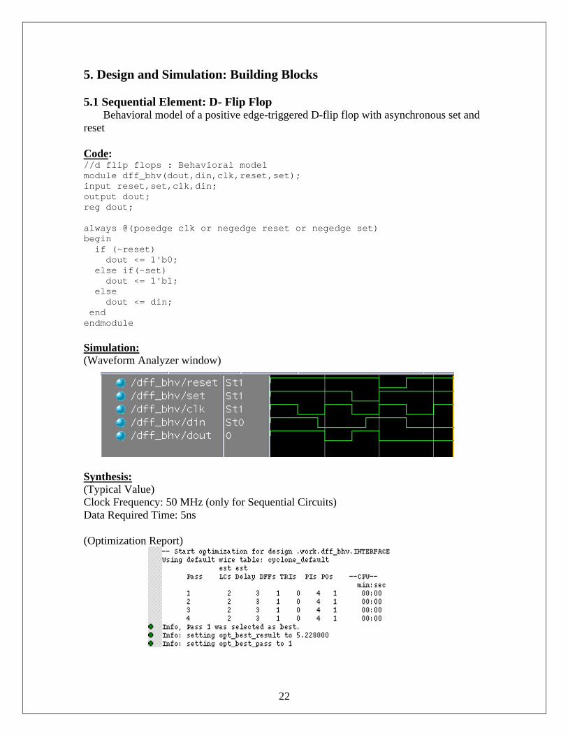
5.1 Sequential Element: D- Flip Flop Behavioral model of a positive edge-triggered D-flip flop with asynchronous set and reset
Code: //d flip flops : Behavioral modelmodule dff_bhv(dout,din,clk,reset,set);input reset,set,clk,din;output dout;reg dout;
always @(posedge clk or negedge reset or negedge set)begin if (~reset) dout <= 1'b0; else if(~set) dout <= 1'b1; else dout <= din; endendmodule
Simulation: (Waveform Analyzer window)
Synthesis:(Typical Value)Clock Frequency: 50 MHz (only for Sequential Circuits)Data Required Time: 5ns
(Optimization Report)
23
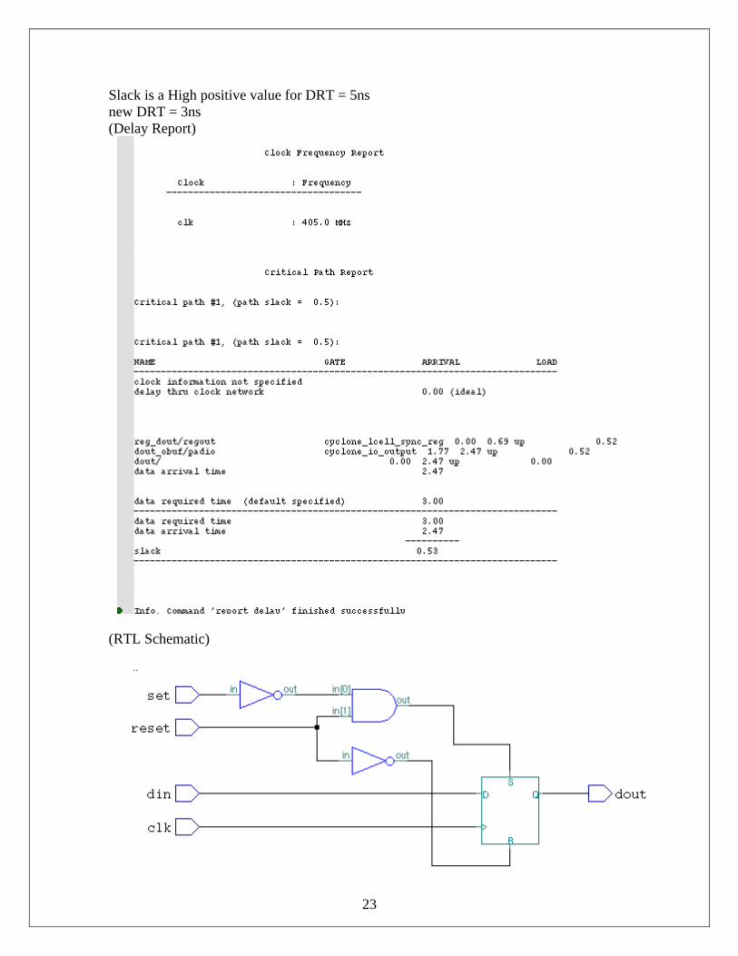
Slack is a High positive value for DRT = 5nsnew DRT = 3ns(Delay Report)
(RTL Schematic)
24
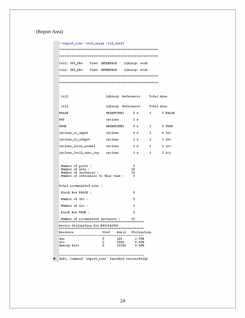
(Report Area)
25
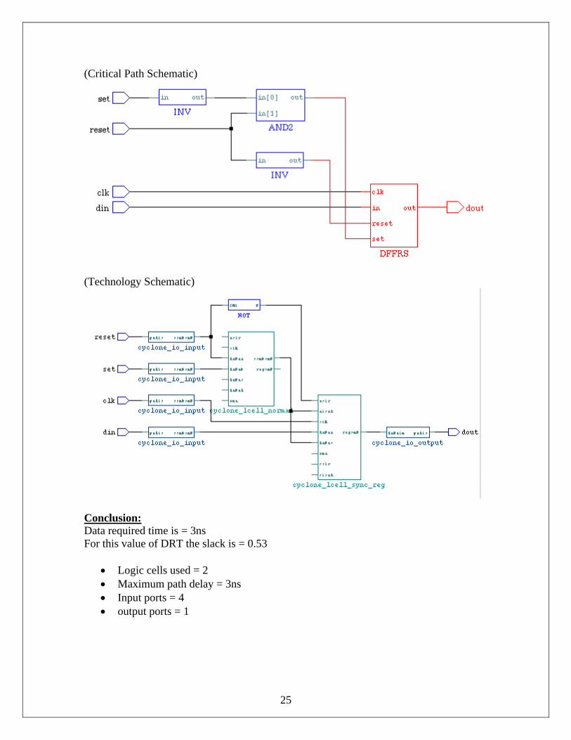
(Critical Path Schematic)
(Technology Schematic)
Conclusion:Data required time is = 3nsFor this value of DRT the slack is = 0.53
Logic cells used = 2 Maximum path delay = 3ns Input ports = 4 output ports = 1
26
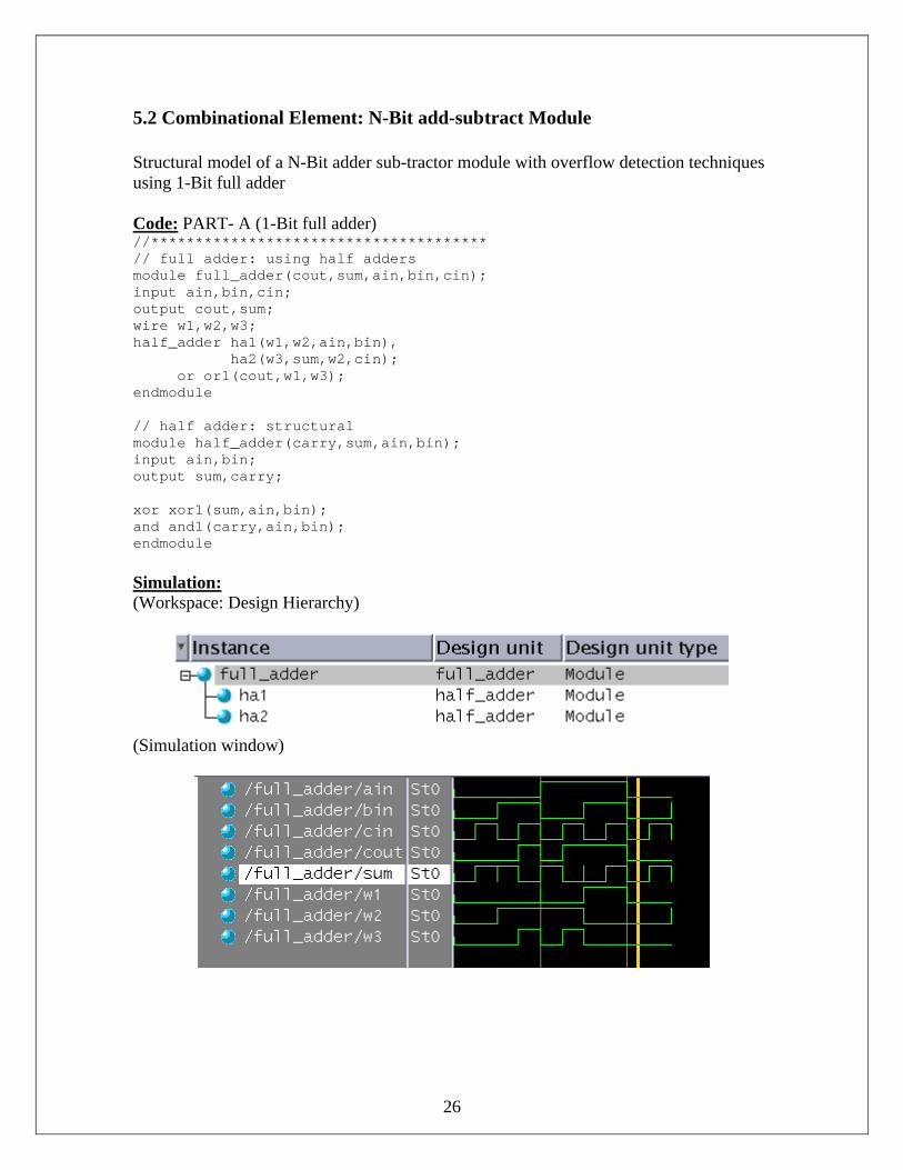
5.2 Combinational Element: N-Bit add-subtract Module
Structural model of a N-Bit adder sub-tractor module with overflow detection techniques using 1-Bit full adder
Code: PART- A (1-Bit full adder)//**************************************// full adder: using half addersmodule full_adder(cout,sum,ain,bin,cin);input ain,bin,cin;output cout,sum;wire w1,w2,w3;half_adder ha1(w1,w2,ain,bin), ha2(w3,sum,w2,cin); or or1(cout,w1,w3);endmodule
// half adder: structuralmodule half_adder(carry,sum,ain,bin);input ain,bin;output sum,carry;
xor xor1(sum,ain,bin);and and1(carry,ain,bin);endmodule
Simulation: (Workspace: Design Hierarchy)
(Simulation window)
27
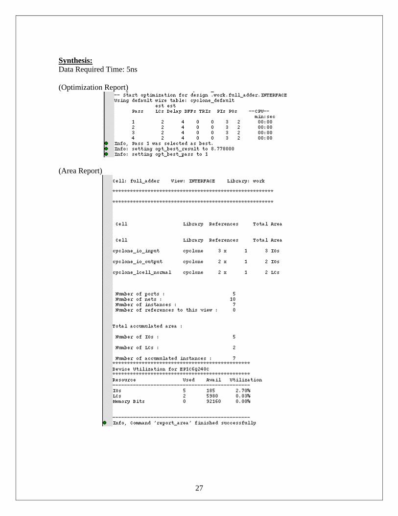
Synthesis:Data Required Time: 5ns
(Optimization Report)
(Area Report)
28
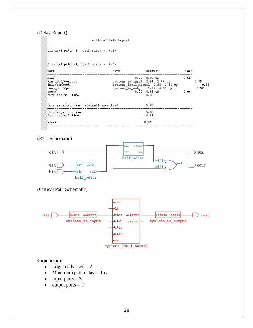
(Delay Report)
(RTL Schematic)
(Critical Path Schematic)
Conclusion: Logic cells used = 2 Maximum path delay = 4ns Input ports = 3 output ports = 2
29
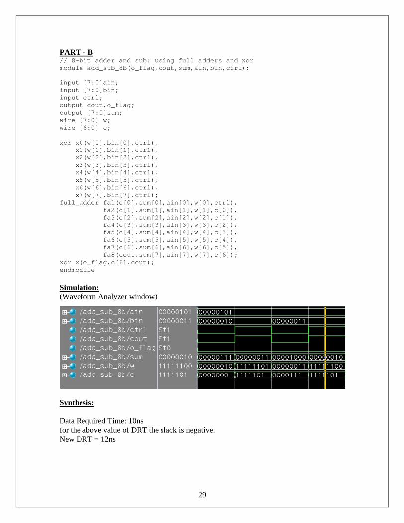
PART - B// 8-bit adder and sub: using full adders and xormodule add_sub_8b(o_flag,cout,sum,ain,bin,ctrl);
input [7:0]ain;input [7:0]bin;input ctrl;output cout,o_flag;output [7:0]sum;wire [7:0] w;wire [6:0] c;
xor x0(w[0],bin[0],ctrl), x1(w[1],bin[1],ctrl), x2(w[2],bin[2],ctrl), x3(w[3],bin[3],ctrl), x4(w[4],bin[4],ctrl), x5(w[5],bin[5],ctrl), x6(w[6],bin[6],ctrl), x7(w[7],bin[7],ctrl);full_adder fa1(c[0],sum[0],ain[0],w[0],ctrl), fa2(c[1],sum[1],ain[1],w[1],c[0]), fa3(c[2],sum[2],ain[2],w[2],c[1]), fa4(c[3],sum[3],ain[3],w[3],c[2]), fa5(c[4],sum[4],ain[4],w[4],c[3]), fa6(c[5],sum[5],ain[5],w[5],c[4]), fa7(c[6],sum[6],ain[6],w[6],c[5]), fa8(cout,sum[7],ain[7],w[7],c[6]);xor x(o_flag,c[6],cout);endmodule
Simulation: (Waveform Analyzer window)
Synthesis:
Data Required Time: 10ns for the above value of DRT the slack is negative.New DRT = 12ns
30
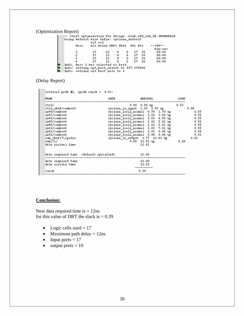
(Optimization Report)
(Delay Report)
Conclusion:
New data required time is = 12nsfor this value of DRT the slack is = 0.39
Logic cells used = 17 Maximum path delay = 12ns Input ports = 17 output ports = 10
31
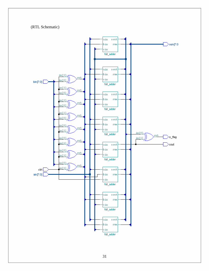
(RTL Schematic)
32
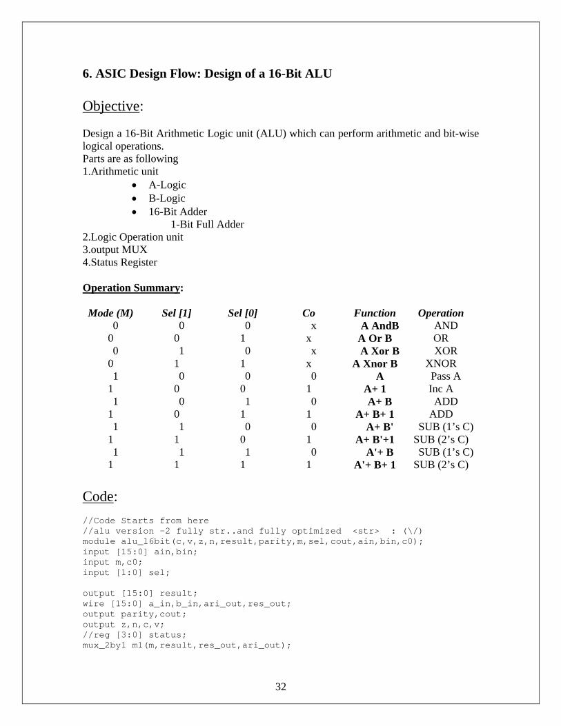
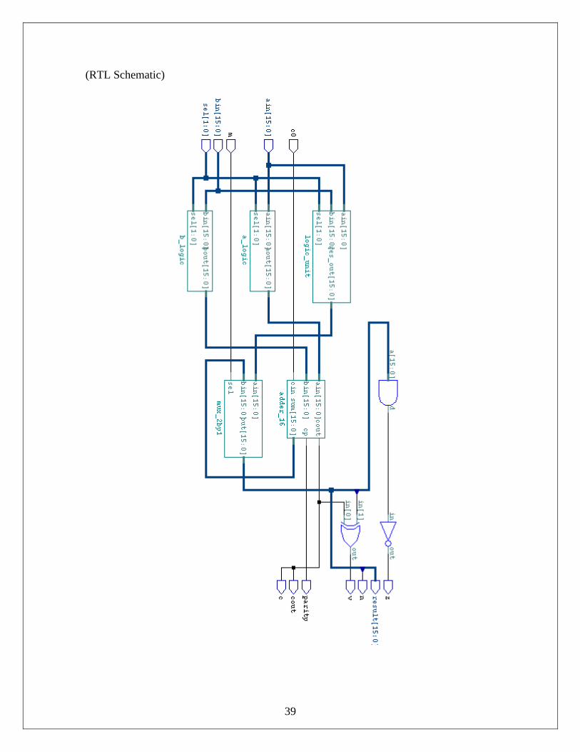
6. ASIC Design Flow: Design of a 16-Bit ALU
Objective:
Design a 16-Bit Arithmetic Logic unit (ALU) which can perform arithmetic and bit-wise logical operations.Parts are as following1.Arithmetic unit
A-Logic B-Logic 16-Bit Adder
1-Bit Full Adder2.Logic Operation unit3.output MUX4.Status Register
Operation Summary:
Mode (M) Sel [1] Sel [0] Co Function Operation0 0 0 x A AndB AND
0 0 1 x A Or B OR0 1 0 x A Xor B XOR
0 1 1 x A Xnor B XNOR1 0 0 0 A Pass A
1 0 0 1 A+ 1 Inc A1 0 1 0 A+ B ADD
1 0 1 1 A+ B+ 1 ADD1 1 0 0 A+ B' SUB (1’s C)
1 1 0 1 A+ B'+1 SUB (2’s C)1 1 1 0 A'+ B SUB (1’s C)
1 1 1 1 A'+ B+ 1 SUB (2’s C)
Code:
//Code Starts from here//alu version -2 fully str..and fully optimized <str> : (\/)module alu_16bit(c,v,z,n,result,parity,m,sel,cout,ain,bin,c0);input [15:0] ain,bin;input m,c0;input [1:0] sel;
output [15:0] result;wire [15:0] a_in,b_in,ari_out,res_out;output parity,cout;output z,n,c,v;//reg [3:0] status;mux_2by1 m1(m,result,res_out,ari_out);
33
b_logic b1(sel,b_in,bin);a_logic a1 (sel,a_in,ain);adder_16 add1(parity,cout,ari_out,a_in,b_in,c0);logic_unit l1(res_out,sel,ain,bin);//s_logic slogic1(status[0],status[1],status[2],status[3],result,cout,o_flow,m);assign z = ~(result[0] & result[1] & result[2] & result[3] & result[4] & result[5] & result[6] & result[7] & result[8] & result[9] & result[10] & result[11] & result[12] & result[13] & result[14] & result[15]); assign n = result [15]; assign v = cout ^ result[15]; assign c = cout;endmodule
//module logical unit : <str> ()\/module logic_unit(res_out,sel,ain,bin);input [15:0] ain,bin;input [1:0]sel;output [15:0] res_out;wire [15:0] and_out,or_out,xor_out,xnor_out;
logic_low_unit llu0(and_out[0],or_out[0],xor_out[0],xnor_out[0],ain[0],bin[0]), llu1(and_out[1],or_out[1],xor_out[1],xnor_out[1],ain[1],bin[1]), llu2(and_out[2],or_out[2],xor_out[2],xnor_out[2],ain[2],bin[2]), llu3(and_out[3],or_out[3],xor_out[3],xnor_out[3],ain[3],bin[3]), llu4(and_out[4],or_out[4],xor_out[4],xnor_out[4],ain[4],bin[4]), llu5(and_out[5],or_out[5],xor_out[5],xnor_out[5],ain[5],bin[5]), llu6(and_out[6],or_out[6],xor_out[6],xnor_out[6],ain[6],bin[6]), llu7(and_out[7],or_out[7],xor_out[7],xnor_out[7],ain[7],bin[7]), llu8(and_out[8],or_out[8],xor_out[8],xnor_out[8],ain[8],bin[8]), llu9(and_out[9],or_out[9],xor_out[9],xnor_out[9],ain[9],bin[9]), llu10(and_out[10],or_out[10],xor_out[10],xnor_out[10],ain[10],bin[10]), llu11(and_out[11],or_out[11],xor_out[11],xnor_out[11],ain[11],bin[11]), llu12(and_out[12],or_out[12],xor_out[12],xnor_out[12],ain[12],bin[12]), llu13(and_out[13],or_out[13],xor_out[13],xnor_out[13],ain[13],bin[13]), llu14(and_out[14],or_out[14],xor_out[14],xnor_out[14],ain[14],bin[14]), llu15(and_out[15],or_out[15],xor_out[15],xnor_out[15],ain[15],bin[15]); mux_4by1 mux41(res_out,sel,and_out,or_out,xor_out,xnor_out); endmodule
34
// 4 by 1 mux : <str> (\/)module mux_4by1(out,sel,i0,i1,i2,i3);input [15:0] i0,i1,i2,i3;output [15:0] out;input [1:0] sel;reg [15:0] out;always @ (i0 or i1 or i2 or i3 or sel)case (sel)2'b00: out=i0;2'b01: out=i1;2'b10: out=i2;2'b11: out=i3;endcaseendmodule
//logical unit low : <str> (\/)module logic_low_unit (and_out,or_out,xor_out,xnor_out,ain,bin);input ain,bin;output and_out,or_out,xor_out,xnor_out;wire w1,w2;//wire and_out,xnor_out;
nand aand1(w1,ain,bin);not nnot1(and_out,w1);nor oor1(w2,ain,bin);not nnot11(or_out,w2);or oor2(xnor_out,and_out,w2);not nnot2(xor_out,xnor_out);endmodule
//mux 2 : <behv> (\/)module mux_2by1(sel,out,ain,bin);input [15:0] ain,bin;input sel;output [15:0] out;reg [15:0] out;always @ (ain or bin or sel)case(sel)1'b0: out=ain;1'b1: out=bin;endcaseendmodule
//logic b : <str> (\/)module b_logic (sel,bout,bin);input [15:0] bin;input [1:0] sel;output [15:0] bout;
b_logic_low bl0(sel,bout[0],bin[0]), bl1(sel,bout[1],bin[1]), bl2(sel,bout[2],bin[2]), bl3(sel,bout[3],bin[3]), bl4(sel,bout[4],bin[4]), bl5(sel,bout[5],bin[5]),
35
bl6(sel,bout[6],bin[6]), bl7(sel,bout[7],bin[7]), bl8(sel,bout[8],bin[8]), bl9(sel,bout[9],bin[9]), bl10(sel,bout[10],bin[10]), bl11(sel,bout[11],bin[11]), bl12(sel,bout[12],bin[12]), bl13(sel,bout[13],bin[13]), bl14(sel,bout[14],bin[14]),bl15(sel,bout[15],bin[15]);
endmodule
//module b logic low : <str> (\/)module b_logic_low (sel,bout,bin);input bin;input [1:0] sel;output bout; wire w1;and an1 (w1,bin,sel[0]);not notn1 (bbar, bin), notn2 (s0_bar, sel[0]);and anda1 (w2, bbar,s0_bar,sel[1]);or orn1 (bout, w1,w2);endmodule
//a logic : <str> (\/)module a_logic(sel,aout,ain);input [15:0] ain;input [1:0] sel;output [15:0] aout;wire w;and nan1 (w,sel[0],sel[1]);xor xorx0 (aout[0],ain[0],w), xorx1 (aout[1],ain[1],w), xorx2 (aout[2],ain[2],w), xorx3 (aout[3],ain[3],w), xorx4 (aout[4],ain[4],w), xorx5 (aout[5],ain[5],w), xorx6 (aout[6],ain[6],w), xorx7 (aout[7],ain[7],w), xorx8 (aout[8],ain[8],w), xorx9 (aout[9],ain[9],w), xorx10 (aout[10],ain[10],w), xorx11 (aout[11],ain[11],w), xorx12 (aout[12],ain[12],w), xorx13 (aout[13],ain[13],w), xorx14 (aout[14],ain[14],w),xorx15 (aout[15],ain[15],w);
endmodule
//16 bit adder : <str> (\/)module adder_16 (cp,cout,sum,ain,bin,cin);input [15:0] ain,bin;input cin;output [15:0] sum;output cp,cout;wire [14:0] c;
36
full_adder fulla0(c[0],sum[0],ain[0],bin[0],cin), fulla1(c[1],sum[1],ain[1],bin[1],c[0]), fulla2(c[2],sum[2],ain[2],bin[2],c[1]), fulla3(c[3],sum[3],ain[3],bin[3],c[2]), fulla4(c[4],sum[4],ain[4],bin[4],c[3]), fulla5(c[5],sum[5],ain[5],bin[5],c[4]), fulla6(c[6],sum[6],ain[6],bin[6],c[5]), fulla7(c[7],sum[7],ain[7],bin[7],c[6]), fulla8(c[8],sum[8],ain[8],bin[8],c[7]), fulla9(c[9],sum[9],ain[9],bin[9],c[8]), fulla10(c[10],sum[10],ain[10],bin[10],c[9]), fulla11(c[11],sum[11],ain[11],bin[11],c[10]), fulla12(c[12],sum[12],ain[12],bin[12],c[11]), fulla13(c[13],sum[13],ain[13],bin[13],c[12]), fulla14(c[14],sum[14],ain[14],bin[14],c[13]), fulla15(cout,sum[15],ain[15],bin[15],c[14]); assign cp = (sum[0]^sum[1]^sum[2]^sum[3]^sum[4]^sum[5]^sum[6]^sum[7]^sum[8]^sum[9]^sum[10]^sum[11]^sum[12]^sum[13]^sum[14]^sum[15]); endmodule
// full adder: <str> (\/)module full_adder(cout,sum,ain,bin,cin);input ain,bin,cin;output cout,sum;wire w1,w2,w3;half_adder ha1(w1,w2,ain,bin), ha2(w3,sum,w2,cin); or or1(cout,w1,w3);endmodule//half adder <str> (\/)module half_adder(carry,sum,ain,bin);input ain,bin;output sum,carry;xor xor11(sum,ain,bin);and and11(carry,ain,bin);endmodule
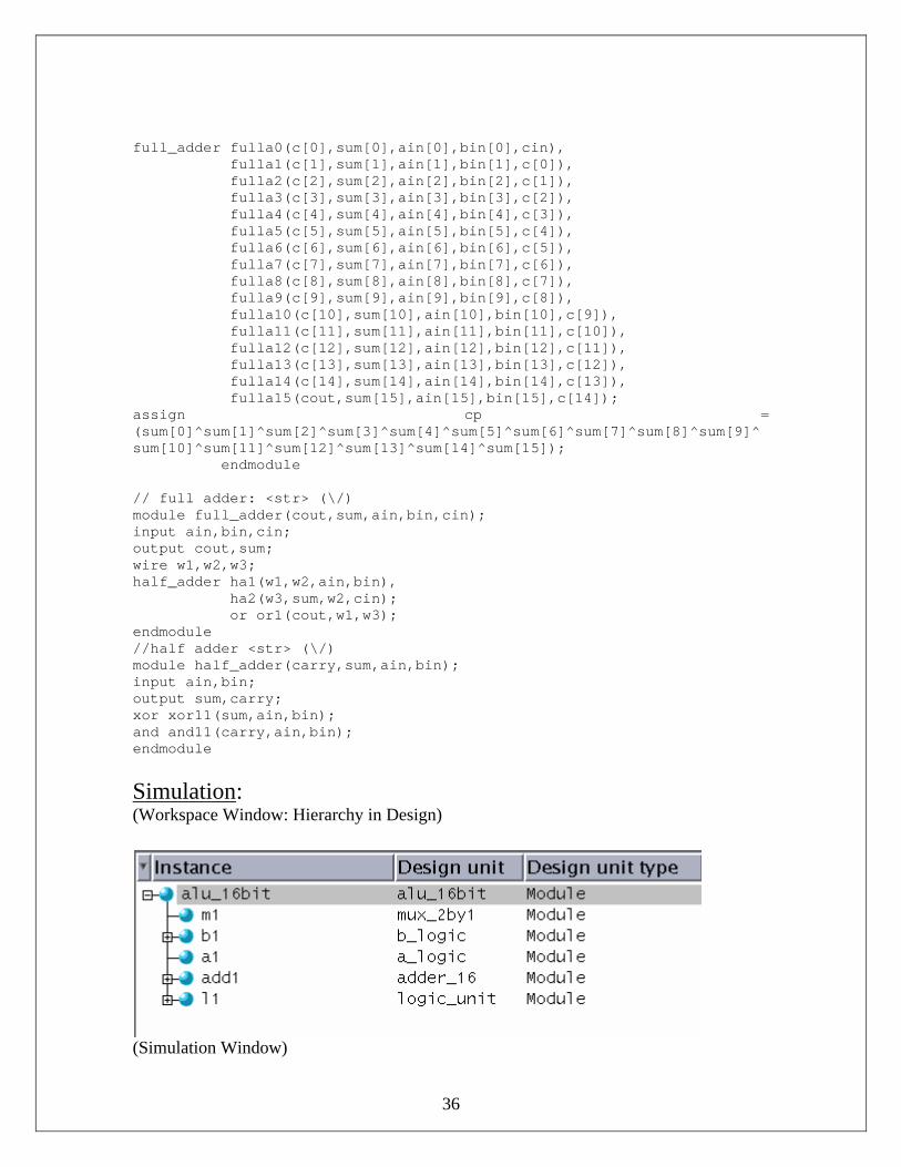
Simulation:(Workspace Window: Hierarchy in Design)
(Simulation Window)
37
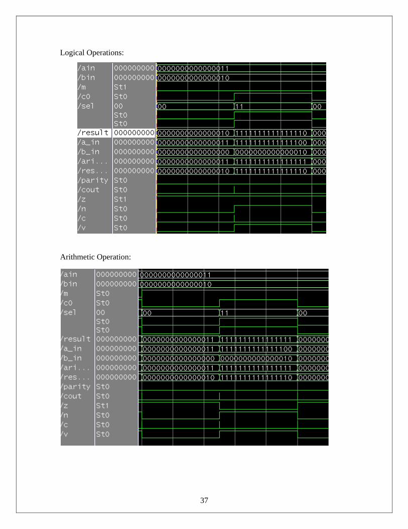
Logical Operations:
Arithmetic Operation:
38
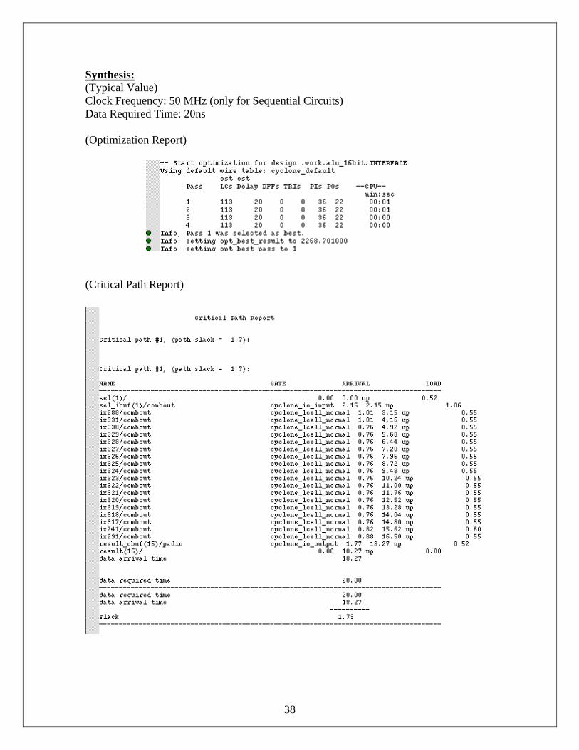
Synthesis:(Typical Value)Clock Frequency: 50 MHz (only for Sequential Circuits)Data Required Time: 20ns
(Optimization Report)
(Critical Path Report)
39
(RTL Schematic)
40
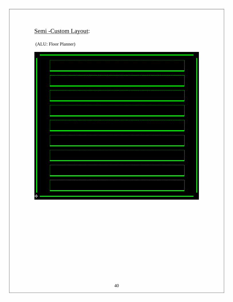
Semi -Custom Layout:
(ALU: Floor Planner)
41
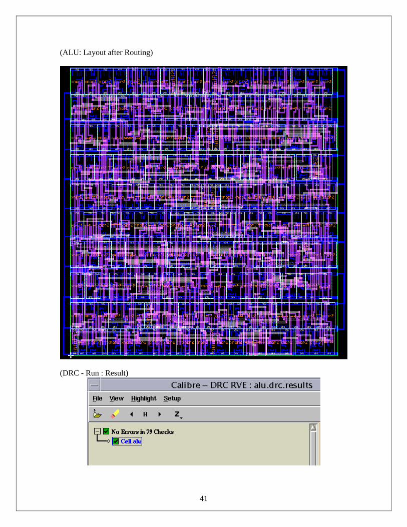
(ALU: Layout after Routing)
(DRC - Run : Result)
42
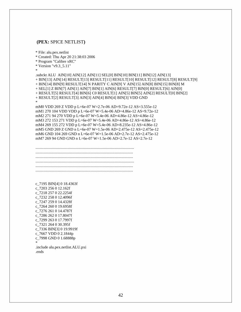
(PEX: SPICE NETLIST)
* File: alu.pex.netlist* Created: Thu Apr 20 21:38:03 2006* Program "Calibre xRC"* Version "v9.3_5.11"* .subckt ALU AIN[10] AIN[12] AIN[11] SEL[0] BIN[10] BIN[11] BIN[12] AIN[13]+ BIN[13] AIN[14] RESULT[13] RESULT[11] RESULT[10] RESULT[12] RESULT[8] RESULT[9]+ BIN[14] BIN[9] RESULT[14] N PARITY C AIN[9] V AIN[15] AIN[8] BIN[15] BIN[8] M+ SEL[1] Z BIN[7] AIN[1] AIN[7] BIN[1] AIN[6] RESULT[7] BIN[0] RESULT[6] AIN[0]+ RESULT[5] RESULT[4] BIN[6] C0 RESULT[1] AIN[5] BIN[5] AIN[2] RESULT[0] BIN[2]+ RESULT[2] RESULT[3] AIN[3] AIN[4] BIN[4] BIN[3] VDD GND* mM0 VDD 269 Z VDD p L=6e-07 W=2.7e-06 AD=9.72e-12 AS=3.555e-12mM1 270 104 VDD VDD p L=6e-07 W=5.4e-06 AD=4.86e-12 AS=9.72e-12mM2 271 94 270 VDD p L=6e-07 W=5.4e-06 AD=4.86e-12 AS=4.86e-12mM3 272 153 271 VDD p L=6e-07 W=5.4e-06 AD=4.86e-12 AS=4.86e-12mM4 269 155 272 VDD p L=6e-07 W=5.4e-06 AD=8.235e-12 AS=4.86e-12mM5 GND 269 Z GND n L=6e-07 W=1.5e-06 AD=2.475e-12 AS=2.475e-12mM6 GND 104 269 GND n L=6e-07 W=1.5e-06 AD=2.7e-12 AS=2.475e-12mM7 269 94 GND GND n L=6e-07 W=1.5e-06 AD=2.7e-12 AS=2.7e-12
....................................................................................................
...................................................................................................
...................................................................................................
c_7195 BIN[4] 0 18.4363fc_7203 256 0 12.162fc_7218 257 0 22.2254fc_7232 258 0 12.4096fc_7247 259 0 14.4328fc_7264 260 0 19.6958fc_7276 261 0 14.4787fc_7286 262 0 17.8047fc_7299 263 0 17.7997fc_7321 264 0 30.395fc_7336 BIN[3] 0 19.9919fc_7667 VDD 0 2.1844pc_7998 GND 0 1.68888p*.include alu.pex.netlist.ALU.pxi.ends
43
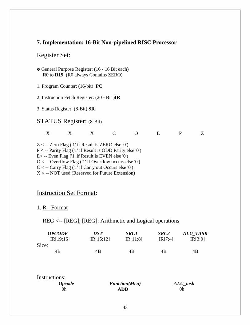
7. Implementation: 16-Bit Non-pipelined RISC Processor
Register Set:
General Purpose Register: (16 - 16 Bit each)R0 to R15: (R0 always Contains ZERO)
1. Program Counter: (16-bit) PC
2. Instruction Fetch Register: (20 - Bit )IR
3. Status Register: (8-Bit) SR
STATUS Register: (8-Bit)
X X X C O E P Z
Z < -- Zero Flag ('1' if Result is ZERO else '0')P < -- Parity Flag ('1' if Result is ODD Parity else '0')E< -- Even Flag ('1' if Result is EVEN else '0')O < -- Overflow Flag ('1' if Overflow occurs else '0')C < -- Carry Flag ('1' if Carry out Occurs else '0')X < -- NOT used (Reserved for Future Extension)
Instruction Set Format:
1. R - Format
REG <-- [REG], [REG]: Arithmetic and Logical operations
OPCODE DST SRC1 SRC2 ALU_TASKIR[19:16] IR[15:12] IR[11:8] IR[7:4] IR[3:0]
Size:4B 4B 4B 4B 4B
Instructions:Opcode Function(Men) ALU_task
0h ADD 0h
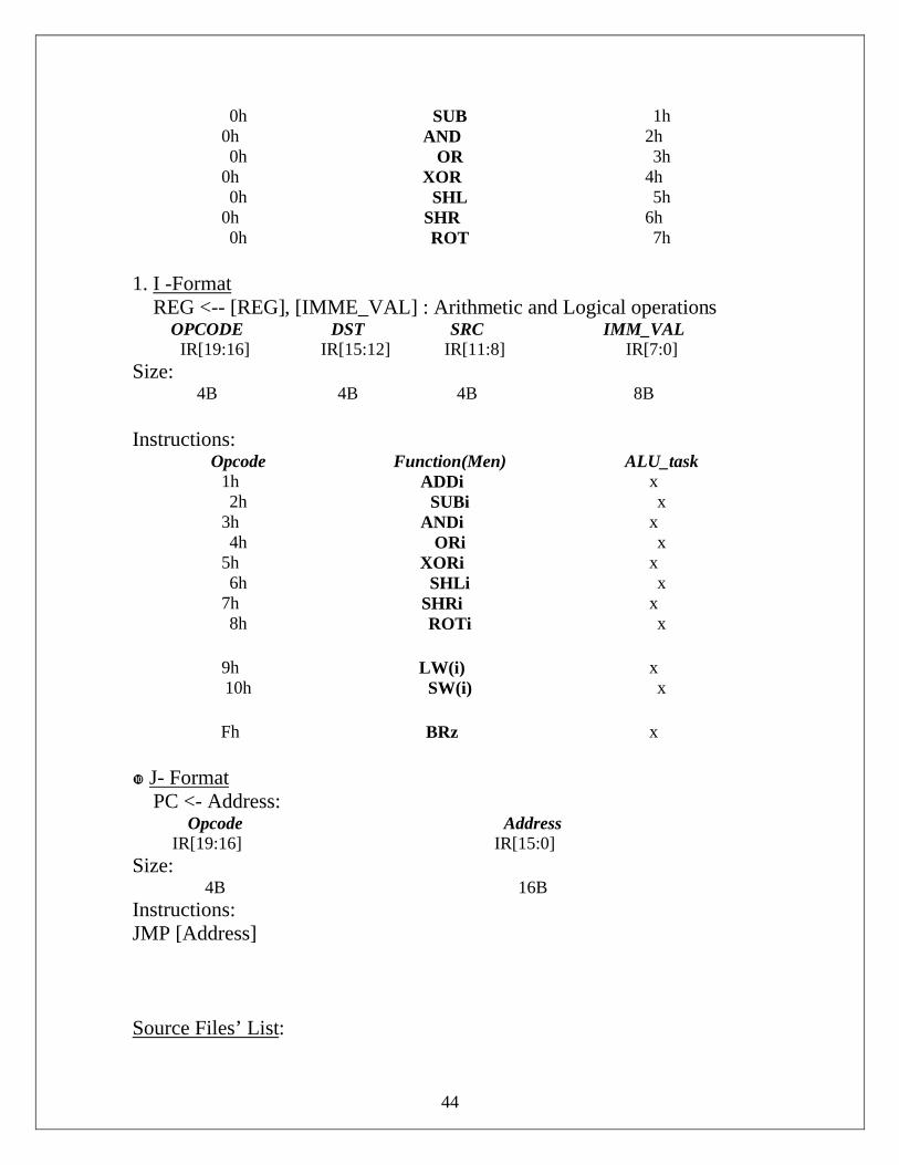
44
0h SUB 1h0h AND 2h0h OR 3h
0h XOR 4h0h SHL 5h
0h SHR 6h0h ROT 7h
1. I -FormatREG <-- [REG], [IMME_VAL] : Arithmetic and Logical operations
OPCODE DST SRC IMM_VALIR[19:16] IR[15:12] IR[11:8] IR[7:0]
Size:4B 4B 4B 8B
Instructions:Opcode Function(Men) ALU_task
1h ADDi x2h SUBi x
3h ANDi x4h ORi x
5h XORi x6h SHLi x
7h SHRi x8h ROTi x
9h LW(i) x10h SW(i) x
Fh BRz x
J- FormatPC <- Address:
Opcode AddressIR[19:16] IR[15:0]
Size:4B 16B
Instructions:JMP [Address]
Source Files’ List:
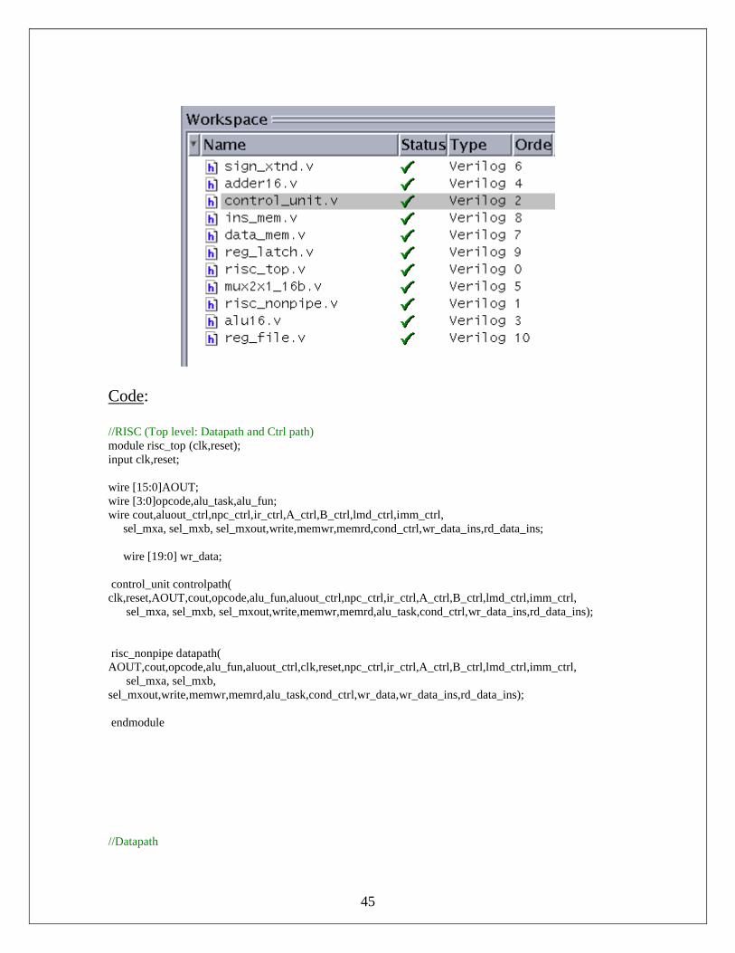
45
Code:
//RISC (Top level: Datapath and Ctrl path)module risc_top (clk,reset);input clk,reset;
wire [15:0]AOUT;wire [3:0]opcode,alu_task,alu_fun;wire cout,aluout_ctrl,npc_ctrl,ir_ctrl,A_ctrl,B_ctrl,lmd_ctrl,imm_ctrl, sel_mxa, sel_mxb, sel_mxout,write,memwr,memrd,cond_ctrl,wr_data_ins,rd_data_ins; wire [19:0] wr_data;
control_unit controlpath( clk,reset,AOUT,cout,opcode,alu_fun,aluout_ctrl,npc_ctrl,ir_ctrl,A_ctrl,B_ctrl,lmd_ctrl,imm_ctrl, sel_mxa, sel_mxb, sel_mxout,write,memwr,memrd,alu_task,cond_ctrl,wr_data_ins,rd_data_ins);
risc_nonpipe datapath( AOUT,cout,opcode,alu_fun,aluout_ctrl,clk,reset,npc_ctrl,ir_ctrl,A_ctrl,B_ctrl,lmd_ctrl,imm_ctrl, sel_mxa, sel_mxb, sel_mxout,write,memwr,memrd,alu_task,cond_ctrl,wr_data,wr_data_ins,rd_data_ins); endmodule
//Datapath
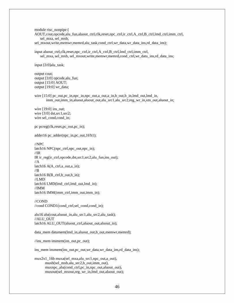
46
module risc_nonpipe ( AOUT,cout,opcode,alu_fun,aluout_ctrl,clk,reset,npc_ctrl,ir_ctrl,A_ctrl,B_ctrl,lmd_ctrl,imm_ctrl, sel_mxa, sel_mxb, sel_mxout,write,memwr,memrd,alu_task,cond_ctrl,wr_data,wr_data_ins,rd_data_ins);
input aluout_ctrl,clk,reset,npc_ctrl,ir_ctrl,A_ctrl,B_ctrl,lmd_ctrl,imm_ctrl, sel_mxa, sel_mxb, sel_mxout,write,memwr,memrd,cond_ctrl,wr_data_ins,rd_data_ins; input [3:0]alu_task;
output cout;output [3:0] opcode,alu_fun;output [15:0] AOUT;output [19:0] wr_data;
wire [15:0] pc_out,pc_in,npc_in,npc_out,a_out,a_in,b_out,b_in,lmd_out,lmd_in, imm_out,imm_in,aluout,aluout_out,alu_src1,alu_src2,reg_wr_in,xtn_out,aluout_in; wire [19:0] ins_out;wire [3:0] dst,src1,src2;wire sel_cond,cond_in;
pc pcreg(clk,reset,pc_out,pc_in);
adder16 pc_adder(npc_in,pc_out,16'h1);
//NPClatch16 NPC(npc_ctrl,npc_out,npc_in);//IRIR ir_reg(ir_ctrl,opcode,dst,src1,src2,alu_fun,ins_out);//Alatch16 A(A_ctrl,a_out,a_in);//Blatch16 B(B_ctrl,b_out,b_in);//LMDlatch16 LMD(lmd_ctrl,lmd_out,lmd_in);//IMMlatch16 IMM(imm_ctrl,imm_out,imm_in);
//COND//cond COND1(cond_ctrl,sel_cond,cond_in);
alu16 alu(cout,aluout_in,alu_src1,alu_src2,alu_task);//ALU_OUTlatch16 ALU_OUT(aluout_ctrl,aluout_out,aluout_in);
data_mem datamem(lmd_in,aluout_out,b_out,memwr,memrd);
//ins_mem insmem(ins_out,pc_out);
ins_mem insmem(ins_out,pc_out,wr_data,wr_data_ins,rd_data_ins);
mux2x1_16b muxa(sel_mxa,alu_src1,npc_out,a_out), muxb(sel_mxb,alu_src2,b_out,imm_out), muxnpc_alu(cond_ctrl,pc_in,npc_out,aluout_out), muxout(sel_mxout,reg_wr_in,lmd_out,aluout_out);
47
sign_xtnd xtender(src2,alu_fun, imm_in);
//reg_file reg_Ro_R15(write,a_in,b_in,src1,src2,dst,reg_wr_in);reg_file_2p reg_Ro_R15(clk,write,a_in,b_in,src1,src2,dst,reg_wr_in);//brz_check iszero(a_out,cond_in);
assign AOUT = a_out;endmodule
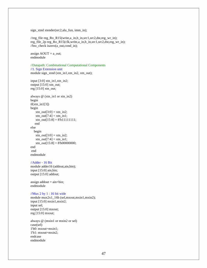
//Datapath: Combinational Computational Components//1. Sign Extension unitmodule sign_xtnd (xtn_in1,xtn_in2, xtn_out);
input [3:0] xtn_in1,xtn_in2;output [15:0] xtn_out;reg [15:0] xtn_out;
always @ (xtn_in1 or xtn_in2)beginif(xtn_in1[3])begin xtn_out[3:0] = xtn_in2; xtn_out[7:4] = xtn_in1; xtn_out[15:8] = 8'b11111111; end else begin xtn_out[3:0] = xtn_in2; xtn_out[7:4] = xtn_in1; xtn_out[15:8] = 8'b00000000;end end endmodule //Adder - 16 Bitmodule adder16 (addout,ain,bin);input [15:0] ain,bin;output [15:0] addout;
assign addout = ain+bin;endmodule
//Mux 2 by 1 : 16 bit widemodule mux2x1_16b (sel,mxout,mxin1,mxin2);input [15:0] mxin1,mxin2;input sel;output [15:0] mxout;reg [15:0] mxout;
always @ (mxin1 or mxin2 or sel)case(sel)1'b0: mxout=mxin1;1'b1: mxout=mxin2;endcaseendmodule
48
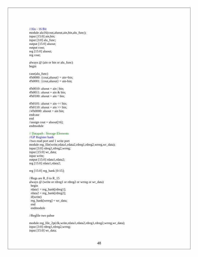
//Alu - 16 Bitmodule alu16(cout,aluout,ain,bin,alu_func);input [15:0] ain,bin;input [3:0] alu_func;output [15:0] aluout;output cout;reg [15:0] aluout;reg cout;
always @ (ain or bin or alu_func)begin
case(alu_func)4'b0000: {cout,aluout} = ain+bin;4'b0001: {cout,aluout} = ain-bin;
4'b0010: aluout = ain | bin;4'b0011: aluout = ain & bin;4'b0100: aluout = ain ^ bin;
4'b0101: aluout = ain << bin;4'b0110: aluout = ain >> bin;//4'b0000: aluout = ain bin;endcaseend//assign cout = aluout[16];endmodule
// Datapath : Storage Elements//GP Register bank//two read port and 1 write portmodule reg_file(write,rdata1,rdata2,rdreg1,rdreg2,wrreg,wr_data);input [3:0] rdreg1,rdreg2,wrreg;input [15:0] wr_data;input write;output [15:0] rdata1,rdata2;reg [15:0] rdata1,rdata2;
reg [15:0] reg_bank [0:15];
//Regs are R_0 to R_15always @ (write or rdreg1 or rdreg2 or wrreg or wr_data) begin rdata1 = reg_bank[rdreg1]; rdata2 = reg_bank[rdreg2]; if(write) reg_bank[wrreg] = wr_data; end endmodule //Regfile two pahse
module reg_file_2p(clk,write,rdata1,rdata2,rdreg1,rdreg2,wrreg,wr_data);input [3:0] rdreg1,rdreg2,wrreg;input [15:0] wr_data;
49
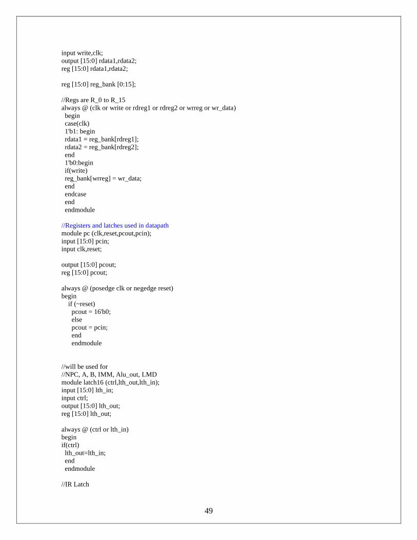
input write,clk;output [15:0] rdata1,rdata2;reg [15:0] rdata1,rdata2;
reg [15:0] reg_bank [0:15];
//Regs are R_0 to R_15always @ (clk or write or rdreg1 or rdreg2 or wrreg or wr_data) begin case(clk) 1'b1: begin rdata1 = reg_bank[rdreg1]; rdata2 = reg_bank[rdreg2]; end 1'b0:begin if(write) reg_bank[wrreg] = wr_data; end endcase end endmodule //Registers and latches used in datapathmodule pc (clk,reset,pcout,pcin);input [15:0] pcin;input clk,reset;
output [15:0] pcout;reg [15:0] pcout;
always @ (posedge clk or negedge reset)begin if (~reset) pcout = 16'b0; else pcout = pcin; end endmodule
//will be used for//NPC, A, B, IMM, Alu_out, LMDmodule latch16 (ctrl,lth_out,lth_in);input [15:0] lth_in;input ctrl;output [15:0] lth_out;reg [15:0] lth_out;
always @ (ctrl or lth_in)beginif(ctrl) lth_out=lth_in; end endmodule //IR Latch
50
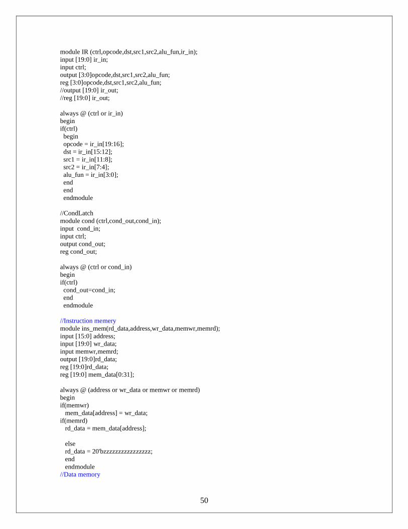
module IR (ctrl,opcode,dst,src1,src2,alu_fun,ir_in);input [19:0] ir_in;input ctrl;output [3:0]opcode,dst,src1,src2,alu_fun;reg [3:0]opcode,dst,src1,src2,alu_fun;//output [19:0] ir_out;//reg [19:0] ir_out;
always @ (ctrl or ir_in)beginif(ctrl) begin opcode = ir_in[19:16]; dst = ir_in[15:12]; src1 = ir_in[11:8]; src2 = ir_in[7:4]; alu_fun = ir_in[3:0]; end end endmodule
//CondLatchmodule cond (ctrl,cond_out,cond_in);input cond_in;input ctrl;output cond_out;reg cond_out;
always @ (ctrl or cond_in)beginif(ctrl) cond_out=cond_in; end endmodule
//Instruction memerymodule ins_mem(rd_data,address,wr_data,memwr,memrd);input [15:0] address;input [19:0] wr_data;input memwr,memrd;output [19:0]rd_data;reg [19:0]rd_data;reg [19:0] mem_data[0:31];
always @ (address or wr_data or memwr or memrd)beginif(memwr) mem_data[address] = wr_data;if(memrd) rd_data = mem_data[address]; else rd_data = 20'bzzzzzzzzzzzzzzzz; end endmodule //Data memory
51
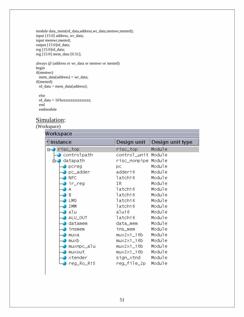
module data_mem(rd_data,address,wr_data,memwr,memrd);input [15:0] address, wr_data;input memwr,memrd;output [15:0]rd_data;reg [15:0]rd_data;reg [15:0] mem_data [0:31];
always @ (address or wr_data or memwr or memrd)beginif(memwr) mem_data[address] = wr_data;if(memrd) rd_data = mem_data[address]; else rd_data = 16'bzzzzzzzzzzzzzzzz; end endmodule
Simulation:(Workspace)
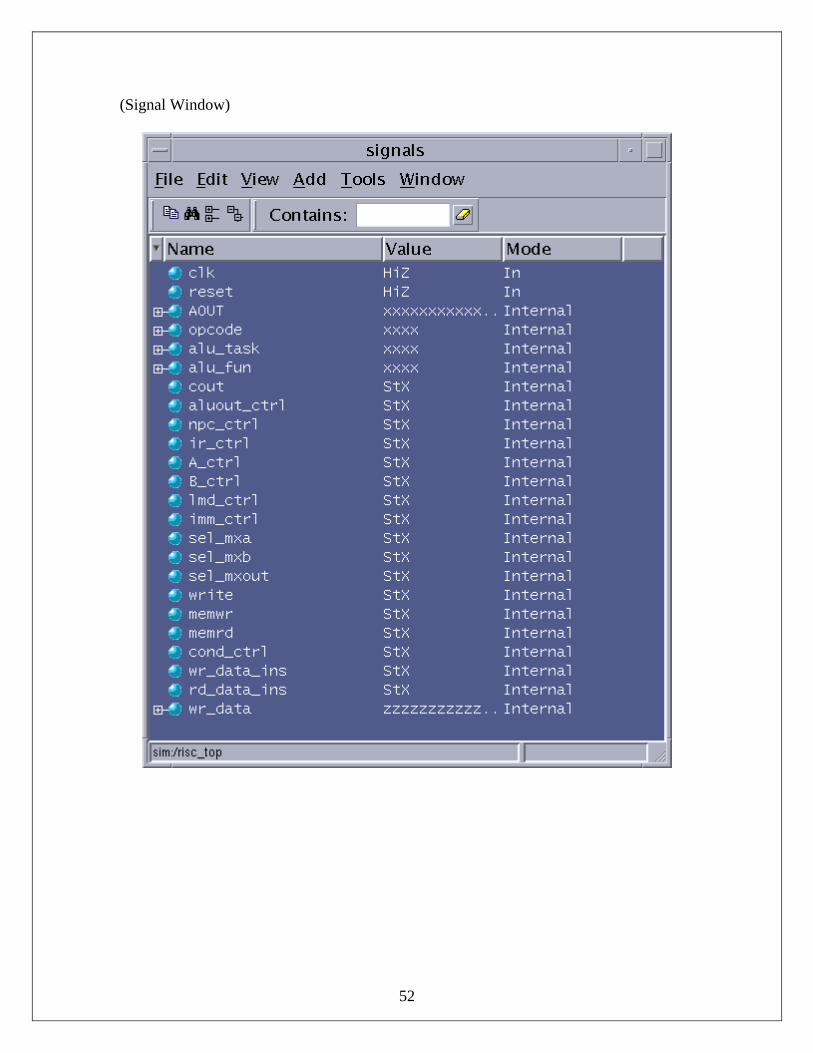
52
(Signal Window)
53
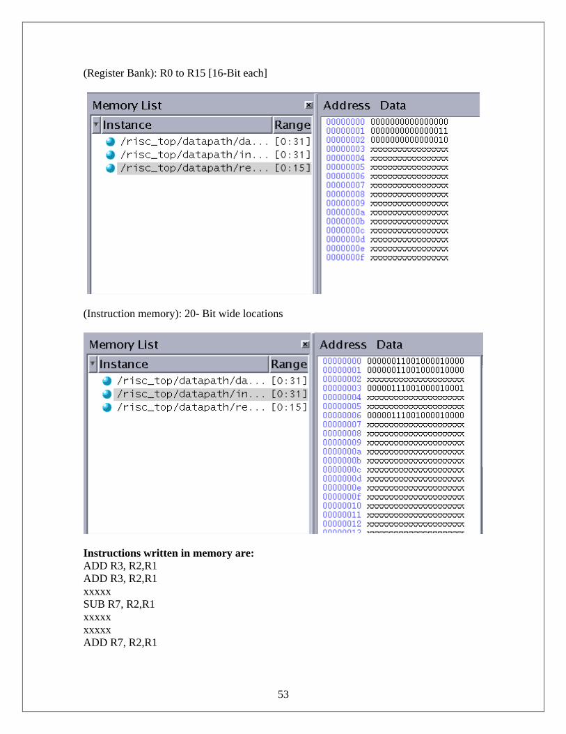
(Register Bank): R0 to R15 [16-Bit each]
(Instruction memory): 20- Bit wide locations
Instructions written in memory are:ADD R3, R2,R1ADD R3, R2,R1xxxxxSUB R7, R2,R1xxxxxxxxxxADD R7, R2,R1
54
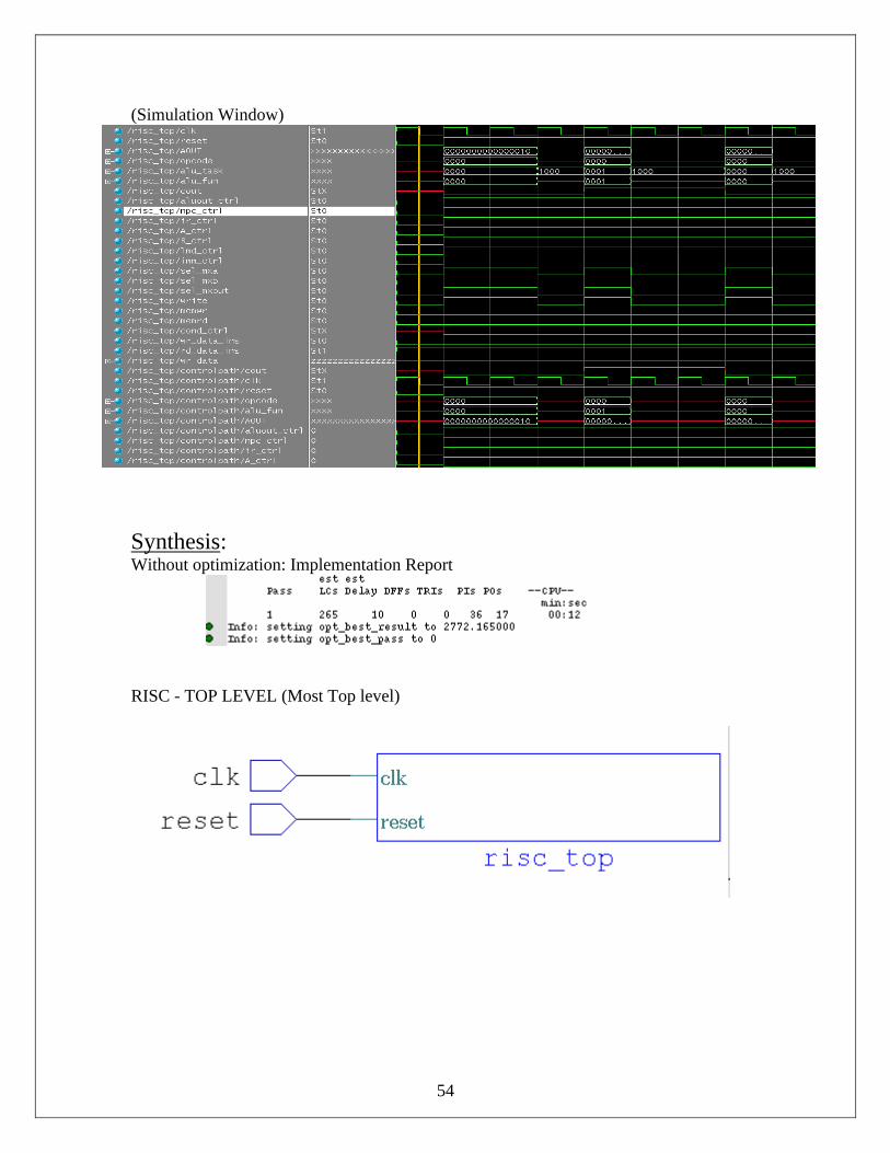
(Simulation Window)
Synthesis:Without optimization: Implementation Report
RISC - TOP LEVEL (Most Top level)
55
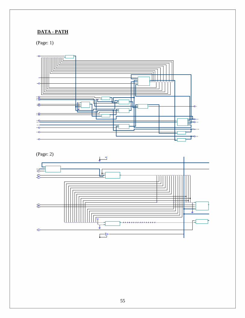
DATA - PATH
(Page: 1)
(Page: 2)
56
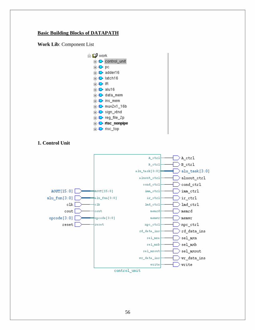
Basic Building Blocks of DATAPATH
Work Lib: Component List
1. Control Unit
57
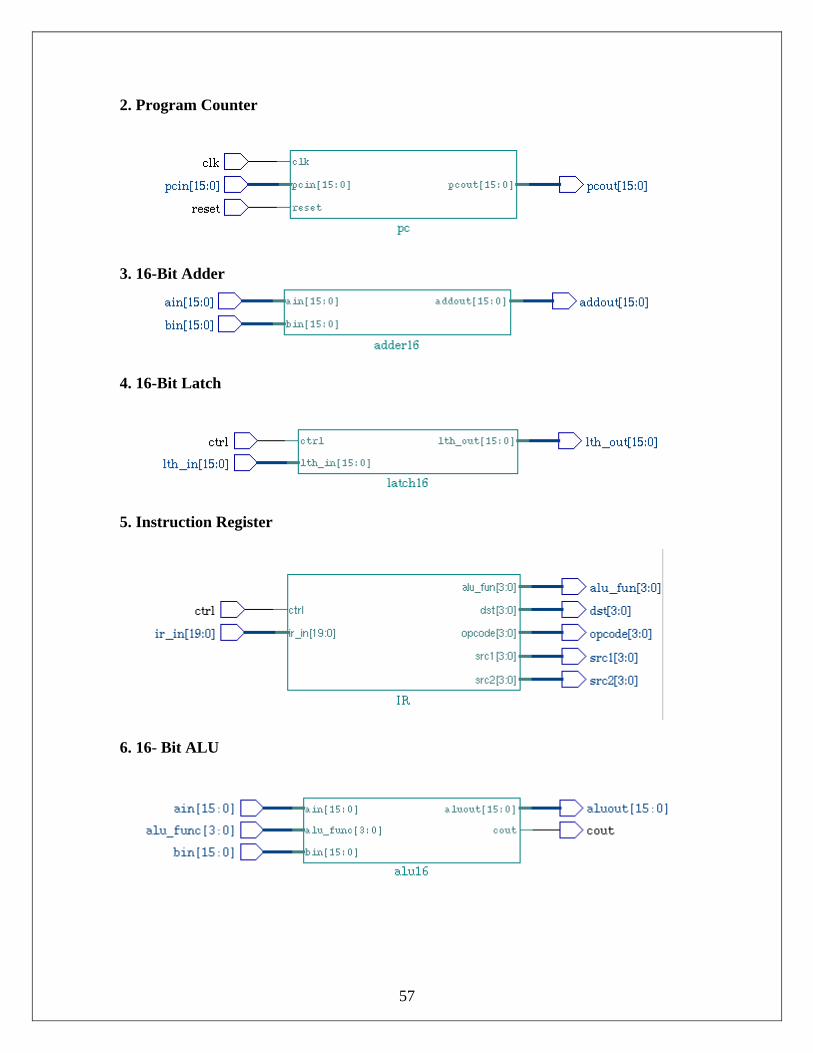
2. Program Counter
3. 16-Bit Adder
4. 16-Bit Latch
5. Instruction Register
6. 16- Bit ALU
58
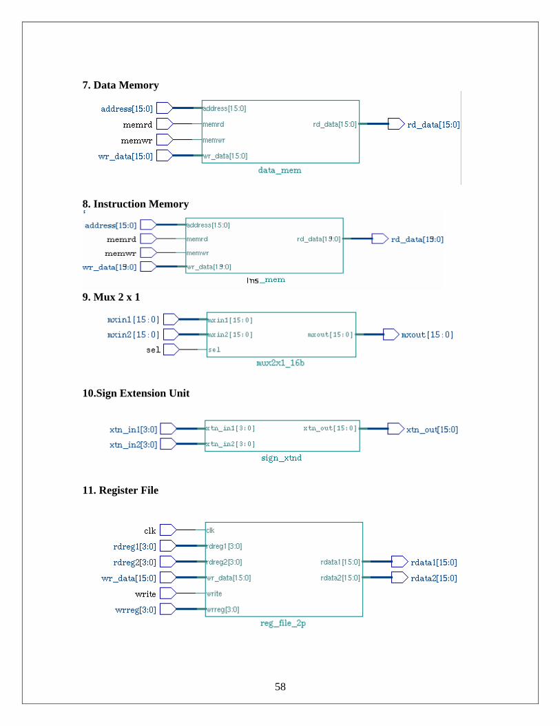
7. Data Memory
8. Instruction Memory
9. Mux 2 x 1
10.Sign Extension Unit
11. Register File
59
12. RISC-Data Path
13. RISC MOST TOP Level
60
ALU with MUX-ed Inputs
Control Path: Synthesis
Clock Frequency: 50MHz DRT: 7ns
(Optimization Report)
61
(Delay Report)
(Area Report)
62
Critical path Schematic
63
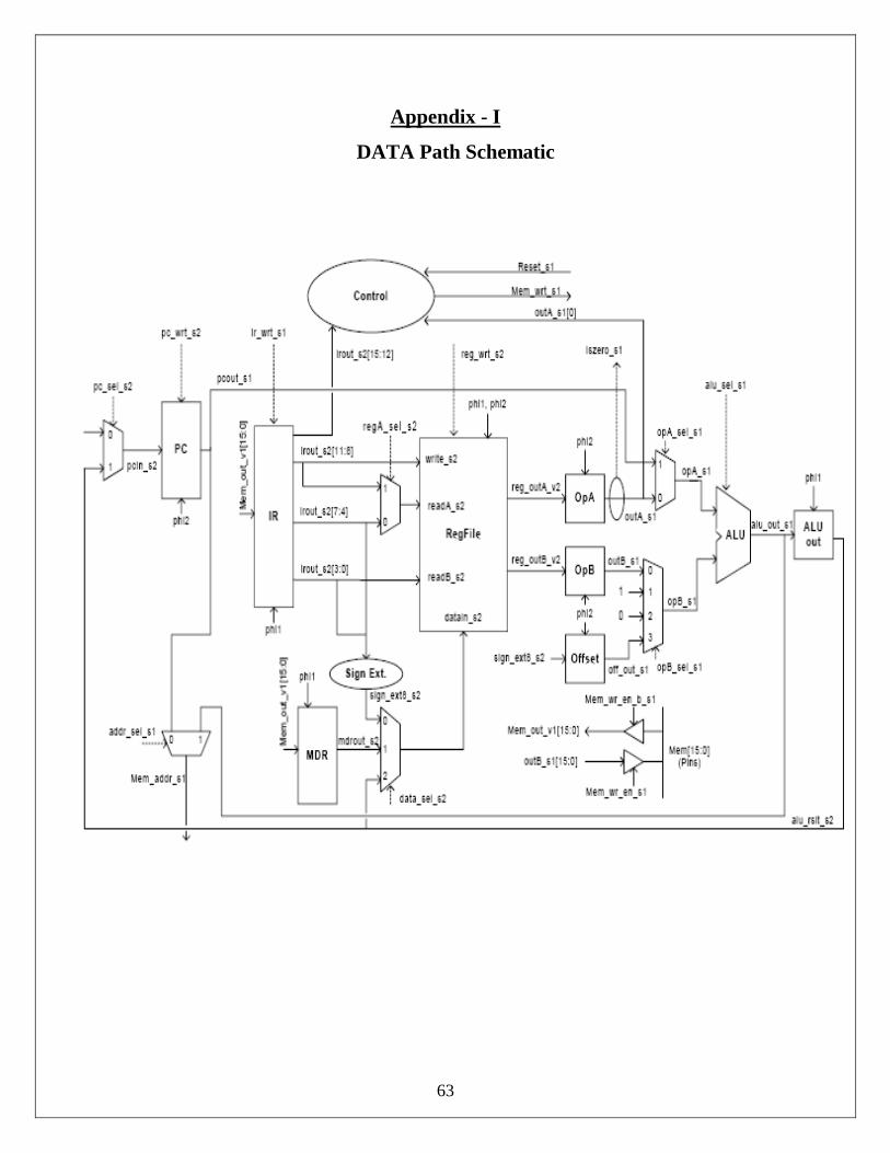
Appendix - I
DATA Path Schematic
64
Appendix – II
Controller State Diagram
65
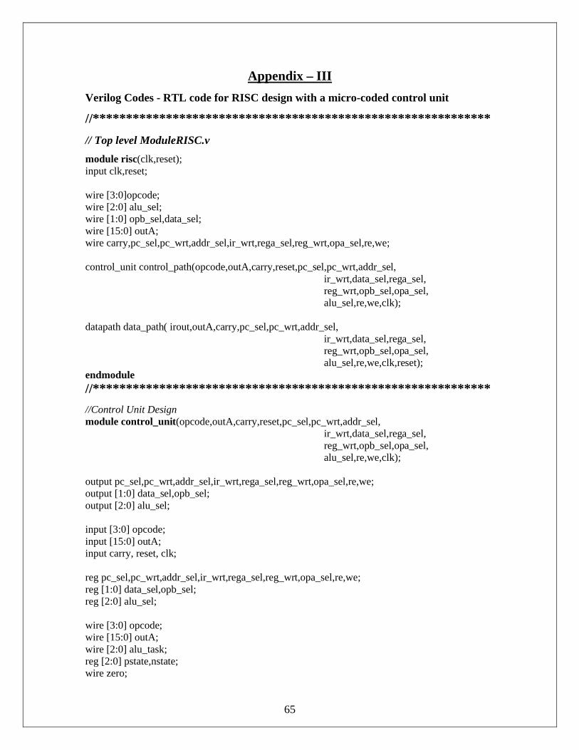
Appendix – III
Verilog Codes - RTL code for RISC design with a micro-coded control unit
//************************************************************
// Top level ModuleRISC.v
module risc(clk,reset);input clk,reset;
wire [3:0]opcode;wire [2:0] alu_sel;wire [1:0] opb_sel,data_sel;wire [15:0] outA;wire carry,pc_sel,pc_wrt,addr_sel,ir_wrt,rega_sel,reg_wrt,opa_sel,re,we;
control_unit control_path(opcode,outA,carry,reset,pc_sel,pc_wrt,addr_sel,ir_wrt,data_sel,rega_sel,reg_wrt,opb_sel,opa_sel,alu_sel,re,we,clk);
datapath data_path( irout,outA,carry,pc_sel,pc_wrt,addr_sel,ir_wrt,data_sel,rega_sel,reg_wrt,opb_sel,opa_sel,alu_sel,re,we,clk,reset);
endmodule
//************************************************************
//Control Unit Designmodule control_unit(opcode,outA,carry,reset,pc_sel,pc_wrt,addr_sel,
ir_wrt,data_sel,rega_sel,reg_wrt,opb_sel,opa_sel,alu_sel,re,we,clk);
output pc_sel,pc_wrt,addr_sel,ir_wrt,rega_sel,reg_wrt,opa_sel,re,we;output [1:0] data_sel,opb_sel;output [2:0] alu_sel;
input [3:0] opcode;input [15:0] outA;input carry, reset, clk;
reg pc_sel,pc_wrt,addr_sel,ir_wrt,rega_sel,reg_wrt,opa_sel,re,we;reg [1:0] data_sel,opb_sel;reg [2:0] alu_sel;
wire [3:0] opcode;wire [15:0] outA;wire [2:0] alu_task;reg [2:0] pstate,nstate;wire zero;
66
assign alu_task = opcode;parameter start=3'b100,s0=3'b000,s1=3'b001,s2=3'b010,s3=3'b011;
assign zero = ((outA == 16'b0)& ((opcode == 4'b1011) | (opcode == 4'b1100)))?1:0;
always @(posedge clk)begin if(~reset)pstate=start;
else pstate = nstate;end
always@(pstate or posedge clk) case (pstate) start: nstate=s0; s0: nstate=s1;
s1: nstate=s2;s2: nstate=s3;s3: nstate=s0;
endcase
always @(posedge clk) case(pstate)//*****************************************************
start: beginpc_sel=0;pc_wrt=0;addr_sel=0;ir_wrt=0;rega_sel=0;reg_wrt=0;opa_sel=0;re=0;we=0;data_sel=2'b0;opb_sel=2'b0;alu_sel=3'b0; end
//****************************************************s0: begin
// Retrieve Instruction Word from Main Memory//Increment Program Counter and Store in ALU Output
pc_sel=0;pc_wrt=0;addr_sel=0;ir_wrt=1;rega_sel=0;reg_wrt=0;opa_sel=1;
67
re=1;we=0;data_sel=2'b00;opb_sel=2'b00;alu_sel=3'b000; end
//*****************************************************s1: begin
//write incremented Program Count//Load Operands into Latches from Register File
case(opcode)4'b0xxx: begin
pc_sel=1;pc_wrt=1;addr_sel=0;ir_wrt=0;rega_sel=0;reg_wrt=0;opa_sel=0;re=0;we=0;data_sel=2'b00;opb_sel=2'b00;alu_sel=alu_task; end
4'b1000: begin// Load Immediate wordpc_sel=1;pc_wrt=1;addr_sel=0;ir_wrt=0;rega_sel=1;reg_wrt=0;opa_sel=0;re=0;we=0;data_sel=2'b00;opb_sel=2'b11;alu_sel=3'b000; end
4'b1001: begin// Load Word Operationpc_sel=1;pc_wrt=1;addr_sel=0;ir_wrt=0;rega_sel=0;reg_wrt=0;opa_sel=0;re=0;we=0;data_sel=2'b00;opb_sel=2'b00;alu_sel=3'b000; end
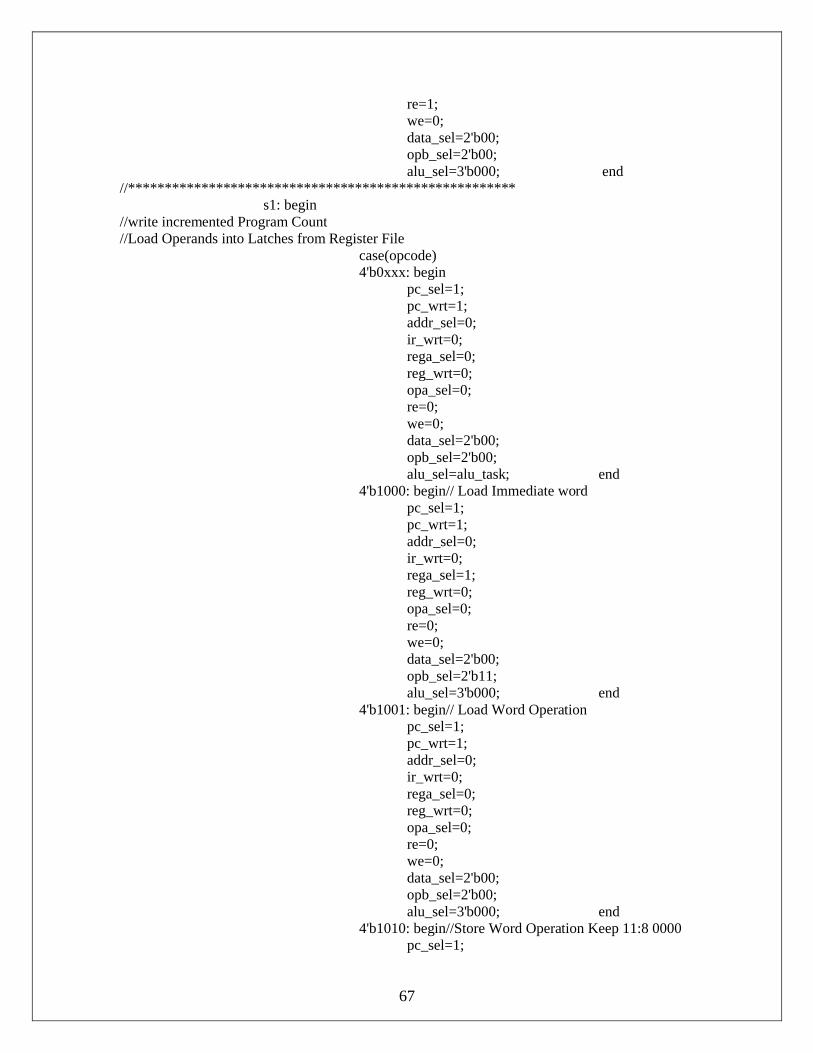
4'b1010: begin//Store Word Operation Keep 11:8 0000pc_sel=1;
68
pc_wrt=1;addr_sel=0;ir_wrt=0;rega_sel=0;reg_wrt=0;opa_sel=0;re=0;we=0;data_sel=2'b00;opb_sel=2'b00;alu_sel=3'b000; end
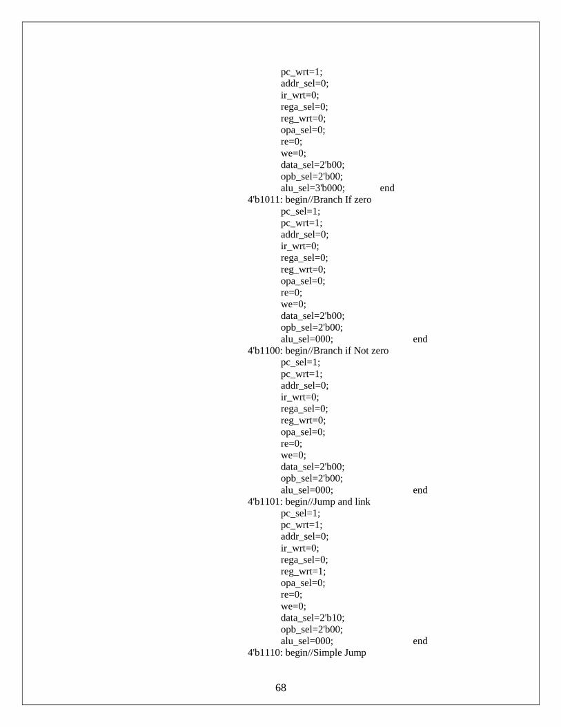
4'b1011: begin//Branch If zeropc_sel=1;pc_wrt=1;addr_sel=0;ir_wrt=0;rega_sel=0;reg_wrt=0;opa_sel=0;re=0;we=0;data_sel=2'b00;opb_sel=2'b00;alu_sel=000; end
4'b1100: begin//Branch if Not zeropc_sel=1;pc_wrt=1;addr_sel=0;ir_wrt=0;rega_sel=0;reg_wrt=0;opa_sel=0;re=0;we=0;data_sel=2'b00;opb_sel=2'b00;alu_sel=000; end
4'b1101: begin//Jump and link pc_sel=1;pc_wrt=1;addr_sel=0;ir_wrt=0;rega_sel=0;reg_wrt=1;opa_sel=0;re=0;we=0;data_sel=2'b10;opb_sel=2'b00;alu_sel=000; end
4'b1110: begin//Simple Jump
69
pc_sel=1;pc_wrt=1;addr_sel=0;ir_wrt=0;rega_sel=0;reg_wrt=0;opa_sel=0;re=0;we=0;data_sel=2'b10;opb_sel=2'b00;alu_sel=000; end
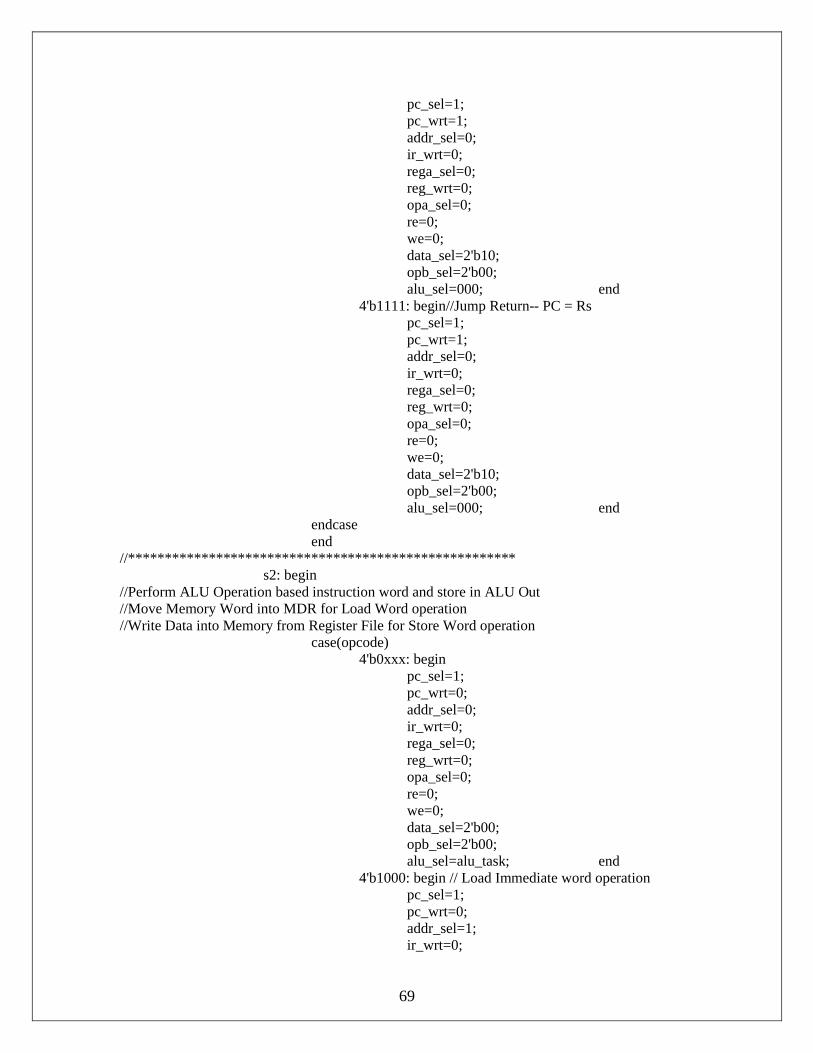
4'b1111: begin//Jump Return-- PC = Rspc_sel=1;pc_wrt=1;addr_sel=0;ir_wrt=0;rega_sel=0;reg_wrt=0;opa_sel=0;re=0;we=0;data_sel=2'b10;opb_sel=2'b00;alu_sel=000; end
endcaseend
//*****************************************************s2: begin
//Perform ALU Operation based instruction word and store in ALU Out//Move Memory Word into MDR for Load Word operation//Write Data into Memory from Register File for Store Word operation
case(opcode)4'b0xxx: begin
pc_sel=1;pc_wrt=0;addr_sel=0;ir_wrt=0;rega_sel=0;reg_wrt=0;opa_sel=0;re=0;we=0;data_sel=2'b00;opb_sel=2'b00;alu_sel=alu_task; end
4'b1000: begin // Load Immediate word operation pc_sel=1;pc_wrt=0;addr_sel=1;ir_wrt=0;
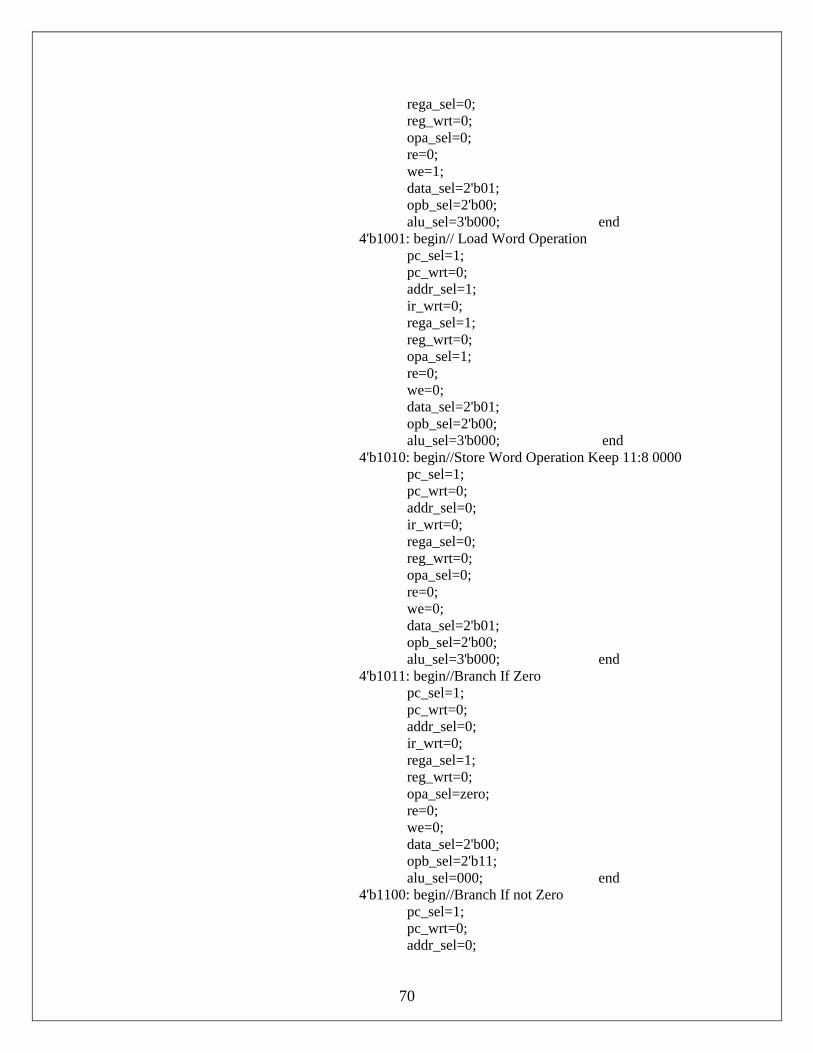
70
rega_sel=0;reg_wrt=0;opa_sel=0;re=0;we=1;data_sel=2'b01;opb_sel=2'b00;alu_sel=3'b000; end
4'b1001: begin// Load Word Operation pc_sel=1;pc_wrt=0;addr_sel=1;ir_wrt=0;rega_sel=1;reg_wrt=0;opa_sel=1;re=0;we=0;data_sel=2'b01;opb_sel=2'b00;alu_sel=3'b000; end
4'b1010: begin//Store Word Operation Keep 11:8 0000pc_sel=1;pc_wrt=0;addr_sel=0;ir_wrt=0;rega_sel=0;reg_wrt=0;opa_sel=0;re=0;we=0;data_sel=2'b01;opb_sel=2'b00;alu_sel=3'b000; end
4'b1011: begin//Branch If Zeropc_sel=1;pc_wrt=0;addr_sel=0;ir_wrt=0;rega_sel=1;reg_wrt=0;opa_sel=zero;re=0;we=0;data_sel=2'b00;opb_sel=2'b11;alu_sel=000; end
4'b1100: begin//Branch If not Zeropc_sel=1;pc_wrt=0;addr_sel=0;
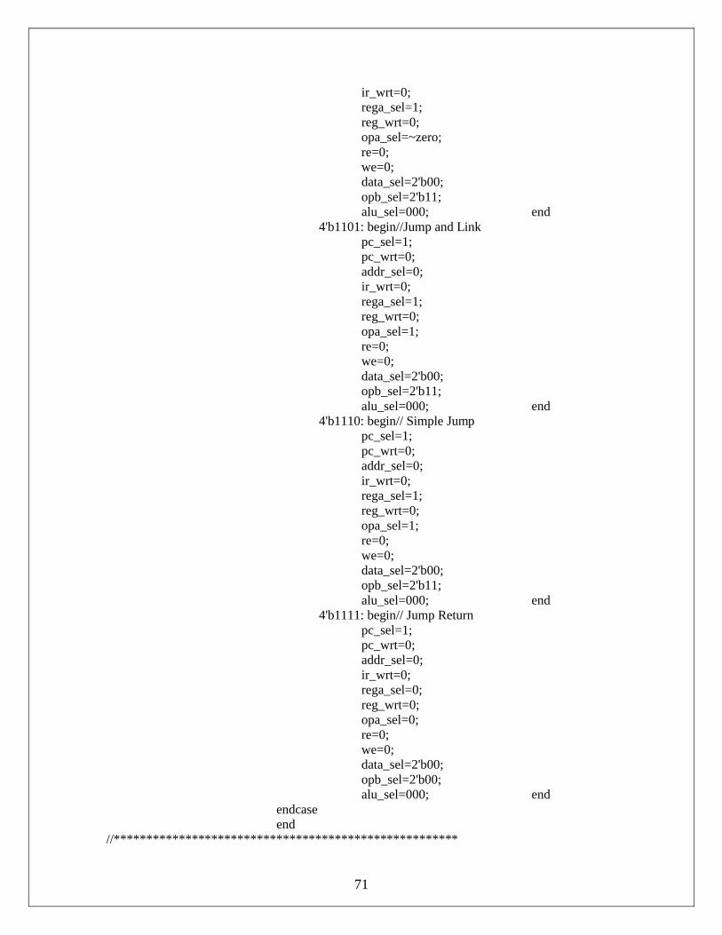
71
ir_wrt=0;rega_sel=1;reg_wrt=0;opa_sel=~zero;re=0;we=0;data_sel=2'b00;opb_sel=2'b11;alu_sel=000; end
4'b1101: begin//Jump and Linkpc_sel=1;pc_wrt=0;addr_sel=0;ir_wrt=0;rega_sel=1;reg_wrt=0;opa_sel=1;re=0;we=0;data_sel=2'b00;opb_sel=2'b11;alu_sel=000; end
4'b1110: begin// Simple Jumppc_sel=1;pc_wrt=0;addr_sel=0;ir_wrt=0;rega_sel=1;reg_wrt=0;opa_sel=1;re=0;we=0;data_sel=2'b00;opb_sel=2'b11;alu_sel=000; end
4'b1111: begin// Jump Returnpc_sel=1;pc_wrt=0;addr_sel=0;ir_wrt=0;rega_sel=0;reg_wrt=0;opa_sel=0;re=0;we=0;data_sel=2'b00;opb_sel=2'b00;alu_sel=000; end
endcaseend
//*****************************************************
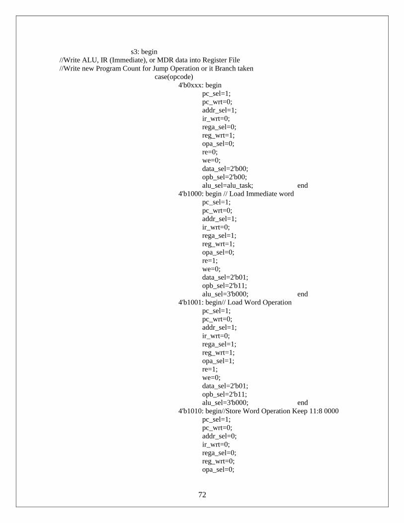
72
s3: begin//Write ALU, IR (Immediate), or MDR data into Register File//Write new Program Count for Jump Operation or it Branch taken
case(opcode)4'b0xxx: begin
pc_sel=1;pc_wrt=0;addr_sel=1;ir_wrt=0;rega_sel=0;reg_wrt=1;opa_sel=0;re=0;we=0;data_sel=2'b00;opb_sel=2'b00;alu_sel=alu_task; end
4'b1000: begin // Load Immediate word pc_sel=1;pc_wrt=0;addr_sel=1;ir_wrt=0;rega_sel=1;reg_wrt=1;opa_sel=0;re=1;we=0;data_sel=2'b01;opb_sel=2'b11;alu_sel=3'b000; end
4'b1001: begin// Load Word Operation pc_sel=1;pc_wrt=0;addr_sel=1;ir_wrt=0;rega_sel=1;reg_wrt=1;opa_sel=1;re=1;we=0;data_sel=2'b01;opb_sel=2'b11;alu_sel=3'b000; end
4'b1010: begin//Store Word Operation Keep 11:8 0000pc_sel=1;pc_wrt=0;addr_sel=0;ir_wrt=0;rega_sel=0;reg_wrt=0;opa_sel=0;
73
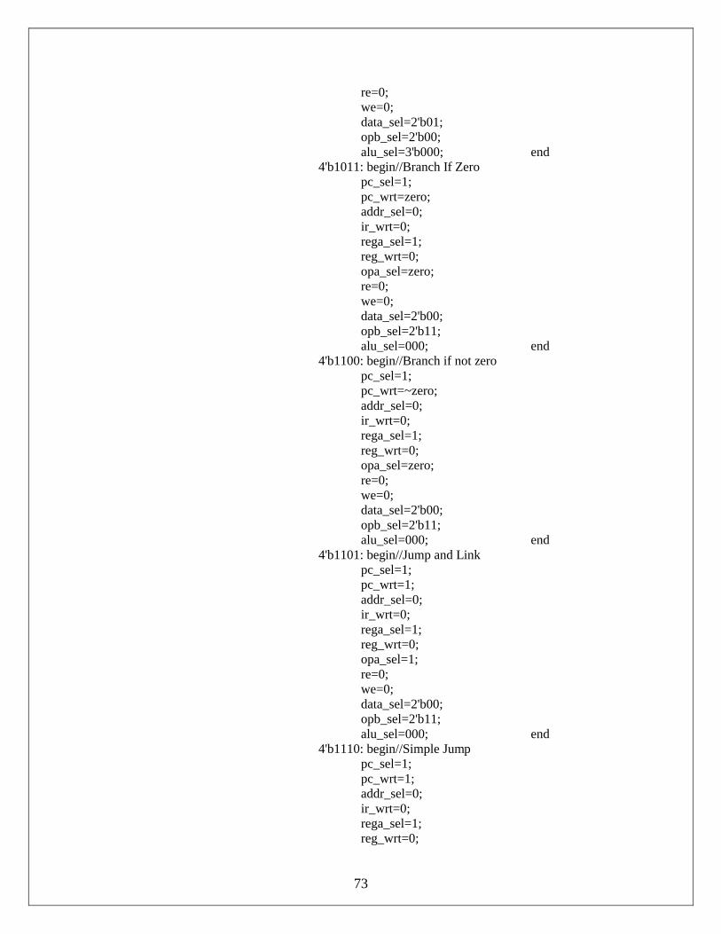
re=0;we=0;data_sel=2'b01;opb_sel=2'b00;alu_sel=3'b000; end
4'b1011: begin//Branch If Zero pc_sel=1;pc_wrt=zero;addr_sel=0;ir_wrt=0;rega_sel=1;reg_wrt=0;opa_sel=zero;re=0;we=0;data_sel=2'b00;opb_sel=2'b11;alu_sel=000; end
4'b1100: begin//Branch if not zeropc_sel=1;pc_wrt=~zero;addr_sel=0;ir_wrt=0;rega_sel=1;reg_wrt=0;opa_sel=zero;re=0;we=0;data_sel=2'b00;opb_sel=2'b11;alu_sel=000; end
4'b1101: begin//Jump and Linkpc_sel=1;pc_wrt=1;addr_sel=0;ir_wrt=0;rega_sel=1;reg_wrt=0;opa_sel=1;re=0;we=0;data_sel=2'b00;opb_sel=2'b11;alu_sel=000; end
4'b1110: begin//Simple Jumppc_sel=1;pc_wrt=1;addr_sel=0;ir_wrt=0;rega_sel=1;reg_wrt=0;
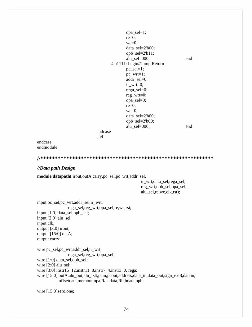
74
opa_sel=1;re=0;we=0;data_sel=2'b00;opb_sel=2'b11;alu_sel=000; end
4'b1111: begin//Jump Returnpc_sel=1;pc_wrt=1;addr_sel=0;ir_wrt=0;rega_sel=0;reg_wrt=0;opa_sel=0;re=0;we=0;data_sel=2'b00;opb_sel=2'b00;alu_sel=000; end
endcaseend
endcaseendmodule
//************************************************************
//Data path Design
module datapath( irout,outA,carry,pc_sel,pc_wrt,addr_sel,ir_wrt,data_sel,rega_sel,reg_wrt,opb_sel,opa_sel,alu_sel,re,we,clk,rst);
input pc_sel,pc_wrt,addr_sel,ir_wrt, rega_sel,reg_wrt,opa_sel,re,we,rst;
input [1:0] data_sel,opb_sel;input [2:0] alu_sel;input clk;output [3:0] irout;output [15:0] outA;output carry;
wire pc_sel,pc_wrt,addr_sel,ir_wrt,rega_sel,reg_wrt,opa_sel;
wire [1:0] data_sel,opb_sel;wire [2:0] alu_sel;wire [3:0] instr15_12,instr11_8,instr7_4,instr3_0, rega;wire [15:0] outA,alu_out,alu_rslt,pcin,pcout,address,data_in,data_out,sign_ext8,datain, offsetdata,memout,opa,Ra,adata,Rb,bdata,opb;
wire [15:0]zero,one;
75
wire clk;
assign zero = 16'b0;assign one = 16'b1;assign irout = instr15_12;assign outA = adata;
//Modules are instantiatedmux2_to_1 pcmux(zero,alu_rslt,pc_sel,pcin);pc programcounter(pcin,pcout,pc_wrt,rst,clk);mux2_to_1 mux_memory(pcout,alu_out,addr_sel,address);ram memory(clk,address,data_in,data_out,re,we);// modified in_data,out_data replaces Memdatainstr_reg IR(data_out,ir_wrt, clk,instr15_12, instr11_8, instr7_4, instr3_0);
mux4b_2_to_1 instrmux(instr11_8,instr7_4,rega_sel,rega);regfile16 regfile(rega,Ra,instr3_0,Rb,instr11_8,datain,reg_wrt,address,data_in,clk);signextender signext(instr7_4,instr3_0,sign_ext8);
mdr memory_data_reg(data_out,memout,clk);mux4_to_1 opbmux(sign_ext8,memout,alu_rslt,zero,data_sel,datain);
opa registera(Ra,adata,clk);opb registerb(Rb,bdata,clk);offset offsetpart(sign_ext8,offsetdata,clk);
mux2_to_1 regamux(adata,pcout,opa_sel,opa);mux4_to_1 regbmux(bdata,zero,one,offsetdata,opb_sel,opb);
alu16b alu(opa,opb,alu_sel,alu_out,carry);aluout finalout(alu_out,alu_rslt,clk);
endmodule
//************************************************************
//ALU Behaviouralmodule alu16b(PORT1, PORT2, ALUCON, ALUOUT, carry);
input [15:0]PORT1,PORT2; input [2:0] ALUCON; output carry; output [15:0] ALUOUT; reg [15:0] ALUOUT; reg carry,temp; always @(ALUCON or PORT1 or PORT2) begin case (ALUCON[2:0])
76
3'b000 : begin {temp,ALUOUT} = (PORT1 + PORT2); //do add //generate appropriate carry for the purpose of slt especially if(PORT1[15]==PORT2[15]) carry=temp; else if(PORT1[15]==1) carry=1;
else carry=0;
end
3'b001 : begin {temp,ALUOUT} = (PORT1 - PORT2); // do subtract //generate appropriate carry for the purpose of slt especially if(PORT1[15]==PORT2[15]) carry=temp; else if(PORT1[15]==1) carry=1;
else carry=0;
end3'b010 : begin ALUOUT = PORT1 & PORT2;temp=0;carry=0; end // do and operation3'b011 : begin ALUOUT = PORT1 | PORT2;temp=0;carry=0; end // do or operation 3'b100 : begin ALUOUT = PORT1 ^ PORT2;temp=0;carry=0; end // do xor operation 3'b101 : begin ALUOUT = ~PORT1 ;temp=0;carry=0; end // do not operation 3'b110 : begin ALUOUT = PORT1 << 1;temp=0;carry=0; end // do SLA operation 3'b111 : begin ALUOUT = PORT1 >> 1;temp=0;carry=0; end // do SRA operation
endcase end endmodule
//************************************************************
//Register File which contains 16 Register of 16 bitsmodule regfile16(add_Rs, out_Rs, add_Rt, out_Rt, add_Rd, data_wr, regwr,addr_sw,data_sw, clk) ;
input [3:0] add_Rs, add_Rt, add_Rd; input regwr, clk; input [15:0] data_wr; output [15:0] out_Rs, out_Rt,addr_sw,data_sw; reg[15:0] Register[15:0]; reg [15:0] out_Rs, out_Rt; wire [15:0] addr_sw,data_sw;
assign addr_sw = out_Rs;
77
assign data_sw = out_Rt; always @ (posedge clk) if(regwr) begin if (add_Rd == 0) Register[add_Rd] = 0;//if it is zero ,the output must be zero only else Register[add_Rd] = data_wr; $display("At this posedge Register %d of Regfile is written %h",add_Rd,data_wr); end
always @ (add_Rs or add_Rt) begin if (add_Rs == 0) out_Rs = 0;// if it is zero register,then give the content as zero only else out_Rs = Register[add_Rs]; if (add_Rt == 0) out_Rt = 0;// if it is zero register,then give the content as zero only else out_Rt = Register[add_Rt]; end
endmodule
//************************************************************
module ram (clk, address, data_in, data_out, re, we);
//parameter DATA_WIDTH = 16 ;//parameter ADDR_WIDTH = 16 ;//parameter RAM_DEPTH = 1 << ADDR_WIDTH;
//--------------Input Ports-----------------------input clk ;input [15:0] address, data_in ;input re ;input we ;
//--------------Inout Ports-----------------------output [15:0] data_out ;
//--------------Internal variables----------------reg [15:0] data ;reg [15:0] mem [15:0];//65535
//--------------Code Starts Here------------------assign data_out = (re)?data:16'bz;
78
// Memory Write Block // Write Operation : When we = 1always @ (posedge clk)begin : MEM_WRITE if ( we ) begin mem[address] = data_in; endend
// Memory Read Block // Read Operation : When re = 1always @ (address or re )begin : MEM_READ if (re) begin data = mem[address]; endend
endmodule
//************************************************************
module instr_reg(instr_data,irwr, clk,instr15_12, instr11_8, instr7_4, instr3_0);input [15:0] instr_data;input irwr,clk;output [3:0] instr15_12, instr11_8, instr7_4, instr3_0;
reg [3:0] instr15_12, instr11_8, instr7_4, instr3_0;
always @(posedge clk)beginif(irwr) begin $display(" At this posedge Instruction register=memory[pc]=%h",instr_data); instr15_12=instr_data[15:12]; instr11_8=instr_data[11:8]; instr7_4=instr_data[7:4]; instr3_0=instr_data[3:0]; endendendmodule
//************************************************************
module pc(indata,outdata,pc_wrt_s2,rst,clk);input [15:0]indata;input clk,pc_wrt_s2,rst;output [15:0] outdata;reg [15:0] outdata;always @ (posedge clk or negedge rst)
79
if(~rst)outdata=0;elsebegin if(pc_wrt_s2) begin outdata=indata; $display("At this posedge contents of pc are %h",outdata); endendendmodule
//************************************************************
module signextender(instr7_4,instr3_0,sign_ext8);input [3:0] instr7_4,instr3_0;output [15:0] sign_ext8;reg [15:0] sign_ext8;wire [7:0] A,B;wire [7:0] in;
assign in={instr7_4,instr3_0};assign A=8'b11111111;assign B=8'b00000000;always @ (in)begin if (in[7]==0)//use the msb to determine extension bits sign_ext8={B,in}; else sign_ext8={A,in};endendmodule
//************************************************************
module offset(sign_ext8,dataout,clk);input [15:0] sign_ext8;input clk;output [15:0] dataout;reg [15:0] dataout;always @ (posedge clk)begindataout=sign_ext8;$display("At this posedge register B=%h",dataout);endendmodule
//************************************************************
module aluout(datain,dataout,clk);input [15:0] datain;input clk;
80
output [15:0] dataout;reg [15:0] dataout;always @ (posedge clk)begindataout=datain;$display("At this posedge of clock register aluout is %h",dataout);endendmodule
module opa(datain,dataout,clk);input [15:0] datain;input clk;output [15:0] dataout;reg [15:0] dataout;always @ (posedge clk)begindataout=datain;$display("At this posedge register B=%h",dataout);endendmodule
//************************************************************
module opb(datain,dataout,clk);input [15:0] datain;input clk;output [15:0] dataout;reg [15:0] dataout;
always @ (posedge clk)begindataout=datain;$display(" At this posedge register B=%h",dataout);endendmodule
//************************************************************
module mux2_to_1(in0,in1,sel,out);input [15:0] in0,in1;input sel;output [15:0] out;reg [15:0] out;always @(sel or in0 or in1)begin case(sel) 1'b0: out=in0; 1'b1: out=in1; endcase
81
endendmodule
//************************************************************
module mux4_to_1(in0,in1,in2,in3,sel,out);input [15:0] in0,in1,in2,in3;input [1:0] sel;output [15:0] out;reg [15:0] out;always @(sel or in0 or in1 or in2 or in3) begin case(sel) 2'b00: out=in0; 2'b01: out=in1; 2'b10: out=in2; 2'b11: out=in3; endcaseendendmodule
//************************************************************
module mux4b_2_to_1(in0,in1,sel,out);input [3:0] in0,in1;input sel;output [3:0] out;reg [3:0] out;always @(sel or in0 or in1)begin case(sel) 1'b0: out=in0; 1'b1: out=in1; endcaseendendmodule
//************************************************************
module mdr(memdatain,memdataout,clk);input [15:0] memdatain;input clk;output [15:0] memdataout;reg [15:0]memdataout;always @ (posedge clk) memdataout=memdatain;endmodule
//************************************************************

82
Bibliography
[1] J.L. Hennessy, D.A.Patterson, Computer Architecture: A Quantitative Approach,
Second Edition, Morgan Kaufmann and Harcourt India, 2000.
[2] J.L. Hennessy, D.A.Patterson, Computer Organization and Design: The
Hardware/Software Interface, Second Edition, Morgan Kaufmann, 2003.
[3] D. J. Smith, HDL Chip Design, International Edition, Doone Publications, 2000
[4] J.F. Wakerly, Digital Design: Principles and Practices, Third Edition, Prentice-Hall,
2000.
[5] J. Bhasker, A VHDL Primer, Third Edition, Pearson, 1999.
[6] A. S. Tanenbaum, Structured Computer Organization, Fourth Edition, Prentice-Hall,
2000.
[7] Yatin Trivedi and others, Verilog HDL, IC, 2000.
[8] Mauriss M Mano, Digital Design, Third Edition, Perason Edition, 2000
[9] Modelsim Help manual, from mentor graphics.[10] www.google.com


![A Fastest RISC Processor using Convolution Method [4] has proposed a 32 bit RISC Processor for implanted application is introduced. Regarding impediment of force and range in installed](https://img.pdfslide.net/doc/110x75/5aa2faaf7f8b9ada698d9d8c/a-fastest-risc-processor-using-convolution-4-has-proposed-a-32-bit-risc-processor.jpg)