Embed Size (px)
Citation preview
MicroBlaze™ 32-bit RISC Processor
Summary Core Reference CR0163 (v2.0) March 10, 2008
The Xilinx® MicroBlaze™ is a fully functional, 32-bit load/store, Wishbone-compliant processor that employs RISC architecture with a streamlined set of single word instructions. This core reference includes an architectural description and on-chip debugging functionality for the processor.
The MicroBlaze is a 32-bit Wishbone-compatible RISC processor, for use in FPGA designs targeting supported Xilinx Spartan® or Virtex® families of physical FPGA devices.
Altium Designer currently supports use of the MicroBlaze processor with the following Xilinx FPGA device families:
Although placed in an Altium Designer-based FPGA project as a MicroBlaze, this is essentially a Wishbone-compliant wrapper that allows use of the 'soft' MicroBlaze processor core.
Spartan®
-II All instructions are 32-bits wide and most execute in a single clock cycle. In addition to fast register access, the MicroBlaze features a user-definable amount of zero-wait state block RAM, with true dual-port access.
Spartan®
-IIE
Spartan®
-3
Spartan®
-3E
Virtex®
-II
Virtex®
-II Pro
Only designs targeting supported Spartan or Virtex FPGA devices may make use of the processor. Should you wish the freedom of a both a device and FPGA Vendor-independent 32-bit system hardware platform, use the available TSK3000A 32-bit RISC processor. Important Notice: Supply of these soft cores under the terms and conditions of the Altium End-User License Agreement does not convey nor imply any patent rights to the supplied technologies. Users are cautioned that a valid MicroBlaze license from Xilinx is required for any use covered by such patent rights, including the implementation of this core in an Integrated Circuit or any other device. The MicroBlaze core is licensed as part of the Xilinx EDK (Embedded Development Kit) – which you will therefore also require. For further information:
Virtex®
-4.
Altium Designer currently supports versions 7.1, 8.1, 8.2, 9.1 and 9.2 of the Xilinx EDK, and version 4.00 of the MicroBlaze soft core processor.
http://www.xilinx.com/ise/embedded_design_prod/platform_studio.htm
Features • 3-stage pipelined RISC processor
• Internal Harvard architecture
• Supports on-chip block RAM and/or external memory
• 4GByte address space
• Wishbone I/O and memory ports for simplified peripheral connection
• Full Viper-based software development tool chain – C compiler/assembler/source-level debugger/profiler
• C-code compatible with other Altium Designer 8-bit and 32-bit Wishbone-compliant processor cores, for easy design migration.
For further information on MicroBlaze features, refer to the following documents, available from www.xilinx.com/microblaze:
• MicroBlaze Product Brief
• MicroBlaze Processor Reference Guide
Available Devices The MicroBlaze device can be found in the FPGA Processors integrated library (FPGA Processors.IntLib), located in the \Library\Fpga folder of the installation.
CR0163 (v2.0) March 10, 2008 1
MicroBlaze 32-bit RISC Processor
RISC Processor Background RISC, or Reduced Instruction Set Computer, is a term that is conventionally used to describe a type of microprocessor architecture that employs a small but highly-optimized set of instructions, rather than the large set of more specialized instructions often found in other types of architectures. This other type of processor is traditionally referred to as CISC, or Complex Instruction Set Computer.
History The early RISC processors came from research projects at Stanford and Berkeley universities in the late 1970s and early 1980s. These processors were designed with a similar philosophy, which has become known as RISC. The basic design architecture of all RISC processors has generally followed the characteristics that came from these early research projects and which can be summarized as follows: • One instruction per clock cycle execution time: RISC processors have a CPI (clock per instruction) of one cycle. This is
due to the optimization of each instruction on the CPU and a technique called pipelining. This technique allows each instruction to be processed in a set number of stages. This in turn allows for the simultaneous execution of a number of different instructions, each instruction being at a different stage in the pipeline.
• Load/Store machine with a large number of internal registers: The RISC design philosophy typically uses a large number (commonly 32) of registers. Most instructions operate on these registers, with access to memory made using a very limited set of Load and Store instructions. This limits the need for continuous access to slow memory for loading and storing data.
• Separate Data Memory and Instruction Memory access paths: Different stages of the pipeline perform simultaneous accesses to memory. This Harvard style of architecture can either be used with two completely different memory spaces, a single dual-port memory space or, more commonly, a single memory space with separate data and instruction caches for the two pipeline stages.
Over the last 20-25 years, RISC processors have been steadily improved and optimized. In one sense, the original simplicity of the RISC architecture has been lost – replaced by super-scalar, multiple-pipelined hardware, often running in the gigahertz range.
“Soft” FPGA Processors With the advent of low-cost, high-capacity programmable logic devices, there has been something of a resurgence in the use of processors with simple RISC architectures. Register-rich FPGAs, with their synchronous design requirements, have found the ideal match when paired with these simple pipelined processors.
As a result, most 32-bit FPGA soft processors are adopting this approach. They could even be considered as “Retro-processors”.
Why use “Soft” Processors? There are a number of benefits to be gained from using soft processors on reconfigurable hardware. The following sections explore some of the more significant of these benefits in more detail.
Field Reconfigurable Hardware For certain specific applications, the ability to change the design once it is in the field can be a significant competitive advantage. Applications in general can benefit from this ability also. It allows commitment to shipping early in the development cycle. It also allows field testing to be used to help drive the latter part of the design cycle without requiring new “board-spins” based on the outcome. This is very similar to the way in which alpha, beta, pre-release and release cycles currently drive the closure of software products.
The ability to update embedded software in a device in the field has long been an advantage enjoyed by designers of embedded systems. With FPGAs, this has now become a reality for the hardware side of the design. For end-users, this translates as “Field Upgradeable Hardware”.
Faster Time to Market FPGAs offer the fastest time to market due to their programmable nature. Design problems, or feature changes, can be made quickly and simply by changing the FPGA design – with no changes in the board-level design.
2 CR0163 (v2.0) March 10, 2008
MicroBlaze 32-bit RISC Processor
Improving and Extending Product Life-Cycles Fast time to market is usually synonymous with a weaker feature set – a traditional trade-off. With FPGA-based system designs you can have the best of both worlds. You can get your product to market quickly with a limited feature set, then follow-up with more extensive features over time, upgrading the product while it is already in the field.
This not only extends product life-cycles but also lowers the risk of entry, allowing new protocols to be added dynamically and hardware bugs to be fixed without product RMA.
Creating Application-Specific Coprocessors Algorithms can easily be moved between hardware and software implementations. This allows the design to be initially implemented in software, later off-loading intensive tasks into dedicated hardware, in order to meet performance objectives. Again, this can happen even after commitment to the board-level design.
Implementing Multiple Processors within a Single Device Extra processors can be added within a single FPGA device, simply by modifying the design with which the device is programmed. Once again, this can be achieved after the board-level design has been finalized and a commitment to production made.
Lowering System Cost Processors, peripherals, memory and I/O interfaces can be integrated into a single FPGA device, greatly reducing system complexity and cost. Once the FPGA-based embedded application moves to 32-bit, cost becomes an even more powerful driver.
As large FPGAs become cheaper, both Hybrids and soft cores move into the same general cost area as dedicated processors. At the heart of this argument is also the idea that once you have paid for the FPGA, any extra IP that you place in the device is free functionality.
Avoiding Processor Obsolescence As products mature, processor supply may become an increasing problem, particularly where the processor is one of many variants supplied by the semiconductor vendor. Switching to a new processor usually requires design software changes or logical hardware changes.
With FPGA implementations, the design can be easily moved to a different device with little or no change to the hardware logic and probably no change to the application software. Peripherals are created dynamically in the hardware, so lack of availability of specific processor variants is never a problem.
The MicroBlaze The MicroBlaze is a 32-bit RISC machine that follows the classic RISC architecture previously described. It is a load/store machine with 32 general purpose registers.
All instructions are 32-bits wide and most execute in a single clock cycle.
In addition to fast register access the MicroBlaze, relying on the commonly available fast block RAM in Spartan and Virtex FPGA devices, also features a user-definable amount of zero-wait state block RAM, with true dual-port access.
Wishbone Bus Interfaces The MicroBlaze uses the Wishbone bus standard. This standard is formally described as a “System-on-Chip Interconnection Architecture for Portable IP Cores”. The current standard is the Revision B.3 Specification, a copy of which is included as part of the software installation and can be found by navigating to the Documentation Library » Designing with FPGAs section of the Knowledge Center panel.
The Wishbone standard is not copyrighted and resides in the public domain. It may be freely copied and distributed by any means. Furthermore, it may be used for the design and production of integrated circuit components without royalties or other financial obligations.
Wishbone OpenBUS Processor Wrappers To normalize access to hardware and peripherals, each of the 32-bit processors supported in Altium Designer has a Wishbone OpenBUS-based FPGA core that 'wraps' around the processor. This enables peripherals defined in the FPGA to be used transparently with any type of processor. An FPGA OpenBUS wrapper around discrete, hard-wired peripherals also allows them to be moved seamlessly between processors.
CR0163 (v2.0) March 10, 2008 3
MicroBlaze 32-bit RISC Processor
The OpenBUS wrappers can be implemented in any FPGA and allow the designer to implement FPGA-based portable cores, taking advantage of the device driver system in Altium Designer for both FPGA-based soft-core peripherals as well as connections to off-chip discrete peripherals and memory devices.
Processor Abstraction System Use of OpenBUS wrappers creates a plug-in processor abstraction system that normalizes the interface to interrupt systems and other hardware specific elements. The system provides an identical interface to the processor's interrupt system, whether soft or hard-vectored. This allows different processors to be used transparently with identical source code bases.
Design Migration With each 32-bit processor encased in a Wishbone OpenBUS wrapper, an embedded software design can be seamlessly moved between soft-core processors, hybrid hard-core processors and discrete processors.
The Wishbone OpenBUS wrapper around the Xilinx MicroBlaze processor makes it architecturally similar to the other 32-bit processors included with Altium Designer, both in terms of its memory map and its pinout. This allows for easy migration from the MicroBlaze to any of the following devices: • TSK3000A – 32-bit RISC processor, device and vendor-independent.
• PPC405A – 'hard' PowerPC® 32-bit RISC processor immersed on the Xilinx Virtex-II Pro.
• Nios® II – 32-bit RISC processor targeted to Altera FPGA platforms.
• PPC405CR – AMCC® PowerPC 32-bit RISC Microprocessor.
• ARM®720T_LH79520 – Sharp Bluestreak® LH79520 with built-in ARM720T (32-bit RISC microprocessor).
Altium Designer also features Wishbone-compliant versions of its TSK52x 8-bit processor. These Wishbone variants, along with true C-code compatibility between these and the MicroBlaze, allow designs to be easily moved between the 8- and 32-bit worlds.
For further information on the TSK3000A, refer to the TSK3000A 32-bit RISC Processor core reference.
For further information on the PPC405A, refer to the PPC405A 32-bit RISC Processor core reference.
For further information on the Nios II, refer to the Nios II 32-bit RISC Processor core reference.
For further information on the TSK52x, refer to the TSK52x MCU core reference.
4 CR0163 (v2.0) March 10, 2008
MicroBlaze 32-bit RISC Processor
Architectural Overview
Symbol
Figure 1. MicroBlaze symbol
Pin Description The pinout of the MicroBlaze has not been fixed to any specific device I/O - allowing flexibility with user application. The MicroBlaze contains only unidirectional pins (inputs or outputs).
Table 1. MicroBlaze pin description
Name Type Polarity/Bus size Description
Control Signals
CLK_I I Rise External (system) clock
RST_I I High External (system) reset
Interrupt Signals
INT_I I 32 Interrupt inputs. Note: The wrapper's interrupt signals are connected internally to the single Interrupt port provided by the MicroBlaze core.
Wishbone External Memory Interface Signals
ME_STB_O O High Strobe signal. When asserted, indicates the start of a valid Wishbone data transfer cycle
ME_CYC_O O High Cycle signal. When asserted, indicates the start of a valid Wishbone bus cycle. This signal remains asserted until the end of the bus cycle, where such a cycle can include multiple data transfers
ME_ACK_I I High Standard Wishbone device acknowledgement signal. When this signal goes High, an external Wishbone slave memory device has finished execution of the requested action and the current bus cycle is terminated
ME_ADR_O O 32 Standard Wishbone address bus, used to select an address in a connected Wishbone slave memory device for writing to/reading from
ME_DAT_I I 32 Data received from an external Wishbone slave memory device
ME_DAT_O O 32 Data to be sent to an external Wishbone slave memory device
CR0163 (v2.0) March 10, 2008 5
MicroBlaze 32-bit RISC Processor
Name Type Polarity/Bus size Description
ME_SEL_O O 4 Select output, used to determine where data is placed on the ME_DAT_O line during a Write cycle and from where on the ME_DAT_I line data is accessed during a Read cycle. Each of the data ports is 32-bits wide with 8-bit granularity, meaning data transfers can be 8-, 16- or 32-bit. The four select bits allow targeting of each of the four active bytes of a port, with bit 0 corresponding to the low byte (7..0) and bit 3 corresponding to the high byte (31..24)
ME_WE_O O Level Write enable signal. Used to indicate whether the current local bus cycle is a Read or Write cycle.
0 = Read 1 = Write
ME_CLK_O O Rise External (system) clock signal (identical to CLK_I), made available for connecting to the CLK_I input of a slave memory device. Though not part of the standard Wishbone interface, this signal is provided for convenience when wiring your design
ME_RST_O O High Reset signal made available for connection to the RST_I input of a slave memory device. This signal goes High when an external reset is issued to the processor on its RST_I pin. When this signal goes Low, the reset cycle has completed and the processor is active again. Though not part of the standard Wishbone interface, this signal is provided for convenience when wiring your design
Wishbone Peripheral I/O Interface Signals
IO_STB_O O High Strobe signal. When asserted, indicates the start of a valid Wishbone data transfer cycle
IO_CYC_O O High Cycle signal. When asserted, indicates the start of a valid Wishbone bus cycle. This signal remains asserted until the end of the bus cycle, where such a cycle can include multiple data transfers
IO_ACK_I I High Standard Wishbone device acknowledgement signal. When this signal goes High, an external Wishbone slave peripheral device has finished execution of the requested action and the current bus cycle is terminated
IO_ADR_O O 24 Standard Wishbone address bus, used to select an internal register of a connected Wishbone slave peripheral device for writing to/reading from
IO_DAT_I I 32 Data received from an external Wishbone slave peripheral device
IO_DAT_O O 32 Data to be sent to an external Wishbone slave peripheral device
IO_SEL_O O 4 Select output, used to determine where data is placed on the IO_DAT_O line during a Write cycle and from where on the IO_DAT_I line data is accessed during a Read cycle. Each of the data ports is 32-bits wide with 8-bit granularity, meaning data transfers can be 8-, 16- or 32-bit. The four select bits allow targeting of each of the four active bytes of a port, with bit 0 corresponding to the low byte (7..0) and bit 3 corresponding to the high byte (31..24)
IO_WE_O O Level Write enable signal. Used to indicate whether the current local bus cycle is a Read or Write cycle.
0 = Read 1 = Write
IO_CLK_O O Rise External (system) clock signal (identical to CLK_I), made available for connecting to the CLK_I input of a slave peripheral device. Though not part of the standard Wishbone interface, this signal is provided for convenience when wiring your design
IO_RST_O O High Reset signal made available for connection to the RST_I input of a slave peripheral device. This signal goes High when an external reset is issued to the processor on its RST_I pin. When this signal goes Low, the reset cycle has completed and the processor is active again. Though not part of the standard Wishbone interface, this signal is provided for convenience when wiring your design
6 CR0163 (v2.0) March 10, 2008
MicroBlaze 32-bit RISC Processor
Configuring the Processor from the Schematic Design The architecture of the MicroBlaze can be configured after placement on the schematic sheet. Simply right-click and choose the command to configure the processor from the pop-up menu that appears (e.g. Configure U_MCU1 (MicroBlaze) for a processor with designator U_MCU1). Alternatively, click on the Configure button, available in the Component Properties dialog for the processor.
The Configure (32-bit Processors) dialog will appear as shown in Figure 2.
Figure 2. Options to configure the architecture of the MicroBlaze
The drop-down field at the top-right of the dialog enables you to choose the type of processor you want to work with. As the pinouts between the 32-bit processors are essentially the same, you can easily change the processor used in your design without having to extensively rewire the external interfaces.
As you select the processor type, the Configure (32-bit Processors) dialog will change accordingly to reflect the architectural options available. The symbol on the schematic will also change to reflect the type of processor and configuration options chosen.
The following sections explore each of the regions in the dialog, providing configurable options specific to the MicroBlaze processor.
Internal Processor Memory This region of the dialog allows you to define the size of the internal memory for the processor. This memory, also referred to as ‘Low’ or ‘Boot’ memory is implemented using true dual port FPGA Block RAM and will contain the boot part of a software application and the interrupt and exception handlers.
Speed-critical (or latency-sensitive) parts of an application should also be placed in this memory space.
The following memory sizes are available to choose from: • 1KB (256 x 32-bit Words)
• 2KB (512 x 32-bit Words)
• 4KB (1K x 32-bit Words)
• 8KB (2K x 32-bit Words)
• 16KB (4K x 32-bit Words)
• 32KB (8K x 32-bit Words)
• 64KB (16K x 32-bit Words)
• 128KB (32K x 32-bit Words)
• 256KB (64K x 32-bit Words)
CR0163 (v2.0) March 10, 2008 7
MicroBlaze 32-bit RISC Processor
• 512KB (128K x 32-bit Words)
• 1MB (256K x 32-bit Words)
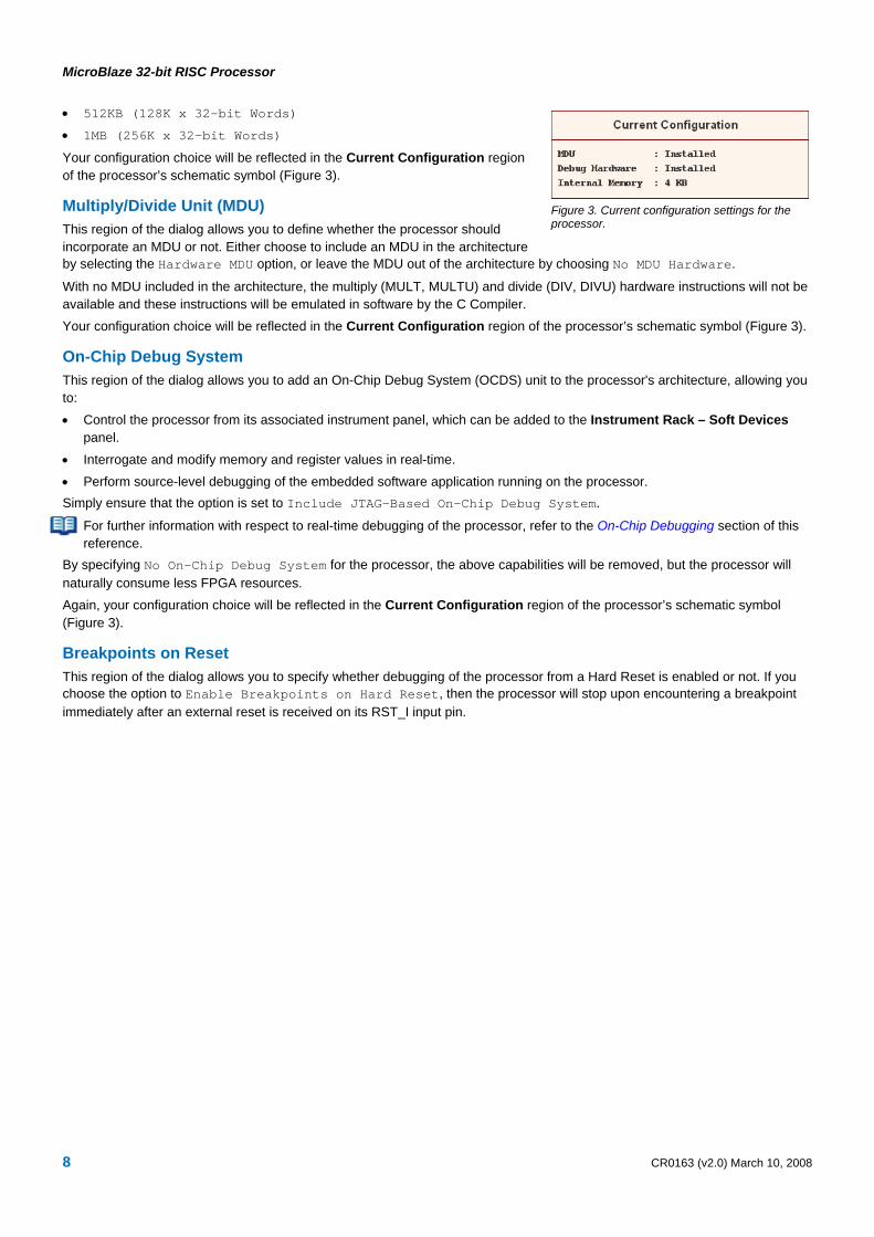
Your configuration choice will be reflected in the Current Configuration region of the processor’s schematic symbol (Figure 3).
Multiply/Divide Unit (MDU) This region of the dialog allows you to define whether the processor should incorporate an MDU or not. Either choose to include an MDU in the architecture by selecting the Hardware MDU option, or leave the MDU out of the architecture by choosing No MDU Hardware.
Figure 3. Current configuration settings for the processor.
With no MDU included in the architecture, the multiply (MULT, MULTU) and divide (DIV, DIVU) hardware instructions will not be available and these instructions will be emulated in software by the C Compiler. Your configuration choice will be reflected in the Current Configuration region of the processor’s schematic symbol (Figure 3).
On-Chip Debug System This region of the dialog allows you to add an On-Chip Debug System (OCDS) unit to the processor's architecture, allowing you to: • Control the processor from its associated instrument panel, which can be added to the Instrument Rack – Soft Devices
panel.
• Interrogate and modify memory and register values in real-time.
• Perform source-level debugging of the embedded software application running on the processor. Simply ensure that the option is set to Include JTAG-Based On-Chip Debug System.
For further information with respect to real-time debugging of the processor, refer to the On-Chip Debugging section of this reference.
By specifying No On-Chip Debug System for the processor, the above capabilities will be removed, but the processor will naturally consume less FPGA resources. Again, your configuration choice will be reflected in the Current Configuration region of the processor’s schematic symbol (Figure 3).
Breakpoints on Reset This region of the dialog allows you to specify whether debugging of the processor from a Hard Reset is enabled or not. If you choose the option to Enable Breakpoints on Hard Reset, then the processor will stop upon encountering a breakpoint immediately after an external reset is received on its RST_I input pin.
8 CR0163 (v2.0) March 10, 2008
MicroBlaze 32-bit RISC Processor
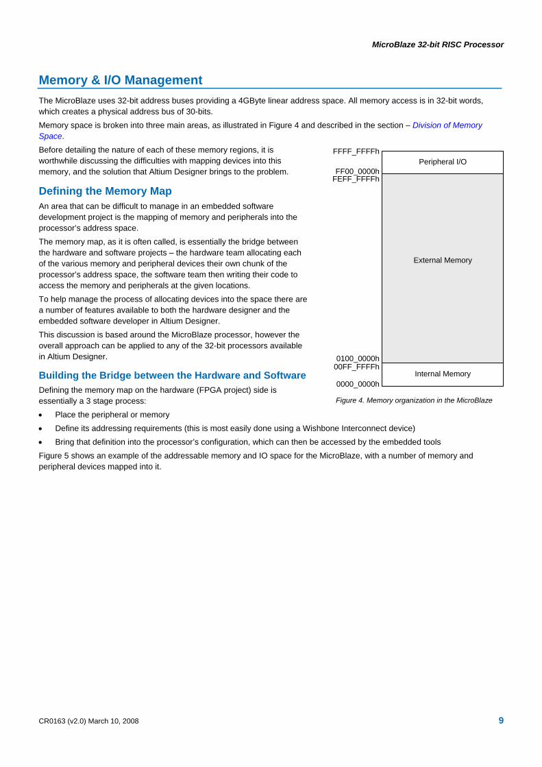
Memory & I/O Management The MicroBlaze uses 32-bit address buses providing a 4GByte linear address space. All memory access is in 32-bit words, which creates a physical address bus of 30-bits.
Memory space is broken into three main areas, as illustrated in Figure 4 and described in the section – Division of Memory Space.
Before detailing the nature of each of these memory regions, it is worthwhile discussing the difficulties with mapping devices into this memory, and the solution that Altium Designer brings to the problem.
0000_0000h
00FF_FFFFh0100_0000h
FEFF_FFFFh
FFFF_FFFFh
FF00_0000hPeripheral I/O
External Memory
Internal Memory
Figure 4. Memory organization in the MicroBlaze
Defining the Memory Map An area that can be difficult to manage in an embedded software development project is the mapping of memory and peripherals into the processor’s address space.
The memory map, as it is often called, is essentially the bridge between the hardware and software projects – the hardware team allocating each of the various memory and peripheral devices their own chunk of the processor’s address space, the software team then writing their code to access the memory and peripherals at the given locations.
To help manage the process of allocating devices into the space there are a number of features available to both the hardware designer and the embedded software developer in Altium Designer.
This discussion is based around the MicroBlaze processor, however the overall approach can be applied to any of the 32-bit processors available in Altium Designer.
Building the Bridge between the Hardware and Software Defining the memory map on the hardware (FPGA project) side is essentially a 3 stage process:
• Place the peripheral or memory
• Define its addressing requirements (this is most easily done using a Wishbone Interconnect device)
• Bring that definition into the processor’s configuration, which can then be accessed by the embedded tools
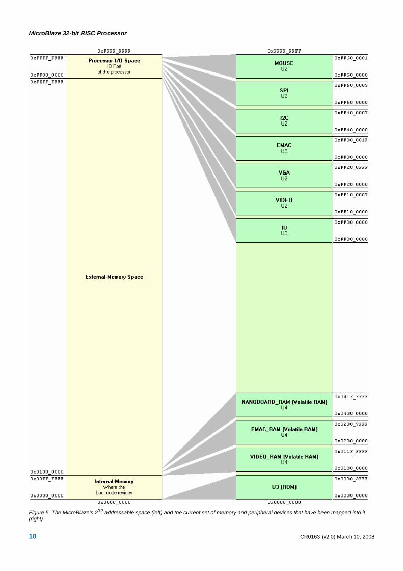
Figure 5 shows an example of the addressable memory and IO space for the MicroBlaze, with a number of memory and peripheral devices mapped into it.
CR0163 (v2.0) March 10, 2008 9
MicroBlaze 32-bit RISC Processor
Figure 5. The MicroBlaze’s 232 addressable space (left) and the current set of memory and peripheral devices that have been mapped into it (right)
10 CR0163 (v2.0) March 10, 2008
MicroBlaze 32-bit RISC Processor
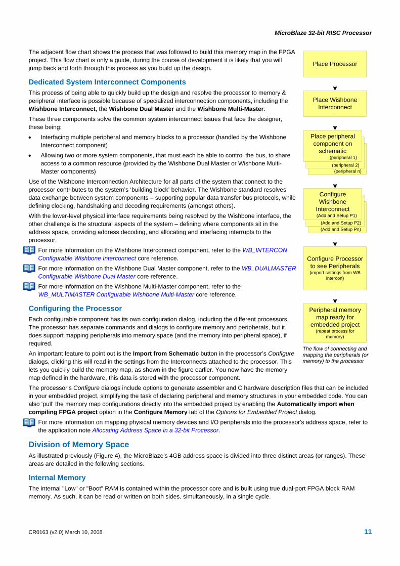
The adjacent flow chart shows the process that was followed to build this memory map in the FPGA project. This flow chart is only a guide, during the course of development it is likely that you will jump back and forth through this process as you build up the design.
Place Processor
Place WishboneInterconnect
Configure Processorto see Peripherals(import settings from WB
intercon)
Peripheral memorymap ready for
embedded project(repeat process for
memory)
(peripheral n) (peripheral 2)
Place peripheralcomponent on
schematic (peripheral 1)
(Add and Setup Pn)
(Add and Setup P2)
ConfigureWishbone
Interconnect (Add and Setup P1)
The flow of connecting and mapping the peripherals (or memory) to the processor
Dedicated System Interconnect Components This process of being able to quickly build up the design and resolve the processor to memory & peripheral interface is possible because of specialized interconnection components, including the Wishbone Interconnect, the Wishbone Dual Master and the Wishbone Multi-Master. These three components solve the common system interconnect issues that face the designer, these being:
• Interfacing multiple peripheral and memory blocks to a processor (handled by the Wishbone Interconnect component)
• Allowing two or more system components, that must each be able to control the bus, to share access to a common resource (provided by the Wishbone Dual Master or Wishbone Multi-Master components)
Use of the Wishbone Interconnection Architecture for all parts of the system that connect to the processor contributes to the system’s ‘building block’ behavior. The Wishbone standard resolves data exchange between system components – supporting popular data transfer bus protocols, while defining clocking, handshaking and decoding requirements (amongst others).
With the lower-level physical interface requirements being resolved by the Wishbone interface, the other challenge is the structural aspects of the system – defining where components sit in the address space, providing address decoding, and allocating and interfacing interrupts to the processor.
For more information on the Wishbone Interconnect component, refer to the WB_INTERCON Configurable Wishbone Interconnect core reference.
For more information on the Wishbone Dual Master component, refer to the WB_DUALMASTER Configurable Wishbone Dual Master core reference.
For more information on the Wishbone Multi-Master component, refer to the WB_MULTIMASTER Configurable Wishbone Multi-Master core reference.
Configuring the Processor Each configurable component has its own configuration dialog, including the different processors. The processor has separate commands and dialogs to configure memory and peripherals, but it does support mapping peripherals into memory space (and the memory into peripheral space), if required. An important feature to point out is the Import from Schematic button in the processor’s Configure dialogs, clicking this will read in the settings from the Interconnects attached to the processor. This lets you quickly build the memory map, as shown in the figure earlier. You now have the memory map defined in the hardware, this data is stored with the processor component.
The processor’s Configure dialogs include options to generate assembler and C hardware description files that can be included in your embedded project, simplifying the task of declaring peripheral and memory structures in your embedded code. You can also ‘pull’ the memory map configurations directly into the embedded project by enabling the Automatically import when compiling FPGA project option in the Configure Memory tab of the Options for Embedded Project dialog.
For more information on mapping physical memory devices and I/O peripherals into the processor's address space, refer to the application note Allocating Address Space in a 32-bit Processor.
Division of Memory Space As illustrated previously (Figure 4), the MicroBlaze's 4GB address space is divided into three distinct areas (or ranges). These areas are detailed in the following sections.
Internal Memory The internal "Low" or "Boot" RAM is contained within the processor core and is built using true dual-port FPGA block RAM memory. As such, it can be read or written on both sides, simultaneously, in a single cycle.
CR0163 (v2.0) March 10, 2008 11
MicroBlaze 32-bit RISC Processor
This memory still has the standard limitation of load delay slots, because the load from memory happens further down the pipeline, after the Execute stage. As a result, any operation that requires loaded data in the cycle immediately after the load will cause the processor to insert a load stall, holding the first half of the pipeline for one cycle while the data becomes available.
Other than this single limitation, the RAM block is as fast as the internal processor registers themselves.
The size of the RAM can vary between 1KB and 16MB, dependent on the availability of embedded block RAM in the target FPGA device used. Memory size is configured in the Internal Processor Memory region of the Configure (32-bit Processors) dialog (see the Configuring the Processor from the Schematic Design section).
Covering the processor's address space between 0000_0000h and 00FF_FFFFh, it will contain the reset and interrupt vectors, as well as any speed or latency-sensitive code or data.
External Memory The processor's Wishbone External Memory Interface is used by both the instruction and data sides of the processor and provides access to the majority of the address space of the processor. It covers the address space between 0100_0000h and FF00_0000h – 1.
External Memory Interface Time-out A simple time-out mechanism for the interface handles the case when attempting to access an address that does not exist, or if the addressed target slave device is not operating correctly. This mechanism ensures that the processor will not be ‘locked’ indefinitely, waiting for an acknowledgement on its ME_ACK_I input.
After the ME_STB_O output is taken High a timer built-in to Altium Designer's MicroBlaze wrapper is started and the actual MicroBlaze processor, which normally times out after 16 cycles, is requested to wait. If, after 4096 cycles of the external clock signal (CLK_I), an acknowledge signal fails to appear from the addressed slave memory device, the wait request to the MicroBlaze is dropped, the processor times out normally and the current data transfer cycle is forcibly terminated.
The ACK_O signal from a slave device should not be used as a ‘long delay’ hand-shaking mechanism. Where such a mechanism needs to be implemented, either use polling or interrupts.
Peripheral I/O The processor's Wishbone Peripheral I/O Interface is a one-way Wishbone Master, handling I/O in a very similar way to external memory. The port can be used to communicate with any Wishbone Slave peripheral device and covers the address space between FF00_0000h and FFFF_FFFFh. This address space of 16MB allows a physical address bus size of 24 bits.
Peripheral I/O Interface Time-out A simple time-out mechanism for the interface handles the case when attempting to access an address that does not exist, or if the addressed target slave device is not operating correctly. This mechanism ensures that the processor will not be ‘locked’ indefinitely, waiting for an acknowledgement on its IO_ACK_I input.
After the IO_STB_O output is taken High a timer built-in to Altium Designer's MicroBlaze wrapper is started and the actual MicroBlaze processor, which normally times out after 16 cycles, is requested to wait. If, after 4096 cycles of the external clock signal (CLK_I), an acknowledge signal fails to appear from the addressed slave peripheral device, the wait request to the MicroBlaze is dropped, the processor times out normally and the current data transfer cycle is forcibly terminated.
The ACK_O signal from a slave peripheral should not be used as a ‘long delay’ hand-shaking mechanism. Where such a mechanism needs to be implemented, either use polling or interrupts.
For more information on connection of slave physical memory and peripheral I/O devices to the processor's Wishbone interfaces, refer to the application note Connecting Memory and Peripheral Devices to a 32-bit Processor.
Data Organization Data organization refers to the ordering of the data during transfers. There are two general types of ordering: • BIG ENDIAN – the most significant portion of an operand is stored at the lower address
• LITTLE ENDIAN – the most significant portion of an operand is stored at the higher address.
The MicroBlaze uses BIG ENDIAN, bit-reversed format to represent data.
12 CR0163 (v2.0) March 10, 2008
MicroBlaze 32-bit RISC Processor
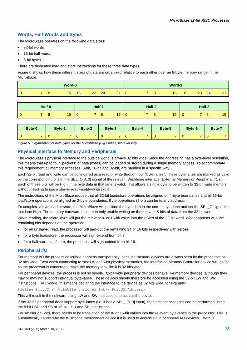
Words, Half-Words and Bytes The MicroBlaze operates on the following data sizes:
• 32-bit words
• 16-bit half-words
• 8-bit bytes.
There are dedicated load and store instructions for these three data types.
Figure 6 shows how these different sizes of data are organized relative to each other over an 8-byte memory range in the MicroBlaze.
Word-0 Word-1
0 7 8 15 16 23 24 31 0 7 8 15 16 23 24 31
Half-0 Half-1 Half-2 Half-3
0 7 8 15 0 7 8 15 0 7 8 15 0 7 8 15
Byte-0 Byte-1 Byte-2 Byte-3 Byte-4 Byte-5 Byte-6 Byte-7
0 7 0 7 0 7 0 7 0 7 0 7 0 7 0 7
Figure 6. Organization of data types for the MicroBlaze (Big Endian, bit-reversed).
Physical Interface to Memory and Peripherals The MicroBlaze's physical interface to the outside world is always 32 bits wide. Since the addressing has a byte-level resolution, this means that up to four "packets" of data (bytes) can be loaded or stored during a single memory access. To accommodate this requirement all memory accesses (8-bit, 16-bit and 32-bit) are handled in a specific way.
Each 32-bit read and write can be considered as a read or write through four "byte-lanes". These byte-lanes are marked as valid by the corresponding bits in the SEL_O[3..0] signal of the relevant Wishbone interface (External Memory or Peripheral I/O). Each of these bits will be High if the byte data in that lane is valid. This allows a single byte to be written to 32-bit wide memory without needing to use a slower read-modify-write cycle.
The instructions of the MicroBlaze require that all 32-bit load/store operations be aligned on 4-byte boundaries and all 16-bit load/store operations be aligned on 2-byte boundaries. Byte operations (8-bit) can be to any address.
To complete a byte load or store, the MicroBlaze will position the byte data in the correct byte-lane and set the SEL_O signal for that lane High. The memory hardware must then only enable writing on the relevant 8-bits of data from the 32-bit word.
When reading, the MicroBlaze will put the relevant 8- or 16-bit value into the LSB's of the 32-bit word. What happens with the remaining bits depends on the operation:
• for an unsigned read, the processor will pad-out the remaining 24 or 16 bits respectively with zeroes
• for a byte load/store, the processor will sign-extend from bit 8
• for a half-word load/store, the processor will sign-extend from bit 16.
Peripheral I/O For memory I/O the process described happens transparently, because memory devices are always seen by the processor as 32 bits wide. Even when connecting to small 8- or 16-bit physical memories, the interfacing Memory Controller device will, as far as the processor is concerned, make the memory look like it is 32 bits wide.
For peripheral devices, the process is not so simple. 32-bit wide peripheral devices behave like memory devices, although they may or may not support individual byte-lanes. These devices should therefore be accessed using the 32-bit LW and SW instructions. For C-code, this means declaring the interface to the device as 32 bits wide, for example: #define Port32 (*(volatile unsigned int*) Port32_Address)
This will result in the software using LW and SW instructions to access the device.
If the 32-bit peripheral does support byte-lanes (i.e. it has a SEL_I[3..0] input), then smaller accesses can be performed using the 8-bit LBU and SB or 16-bit LHU and SH instructions.
For smaller devices, there needs to be translation of the 8- or 16-bit values into the relevant byte-lanes in the processor. This is automatically handled by the Wishbone Interconnect device if it is used to access slave peripheral I/O devices. There is,
CR0163 (v2.0) March 10, 2008 13
MicroBlaze 32-bit RISC Processor
however, some hardware penalty for this since it requires an extra 4:1 8-bit multiplexer for 8-bit devices or a 2:1 16-bit multiplexer for 16-bit devices.
16-bit peripheral devices should be accessed using the 16-bit LHU and SH instructions. For C-code, this means declaring the interface to the device as 16 bits wide, for example: #define Port16 (*(volatile unsigned short*) Port16_Address)
This will result in the software using LHU and SH instructions to access the device.
8-bit peripheral devices should be accessed using the 8-bit LBU and SB instructions. For C-code, this means declaring the interface to the device as 8 bits wide, for example: #define Port8 (*(volatile unsigned char*) Port8_Address)
This will result in the software using LBU and SB instructions to access the device.
There are some trade-offs that may need to be considered when deciding whether to use 8-, 16- or 32-bit wide devices. It may require significantly less hardware to implement a single 32-bit wide I/O port than it would to implement four separate 8-bit ports. If however, the natural format of the data packets is 8-bits and hardware size is not a constraint, then it may be better to use 8-bit ports since there will be no need to use software to break up a 32-bit value into smaller components.
If you are only accessing 8-bits at any one time, then software may also execute faster when using 8-bit wide peripherals, since there is need for extra instructions to extract the 8-bit values from the 32-bit values.
Hardware Description For detailed information about the hardware and functionality of the MicroBlaze processor, including internal registers, refer to the following reference guide, available from the Xilinx website:
• MicroBlaze Processor Reference Guide
Interrupts The 32 external interrupt input signals that can be wired to the wrapper's Peripheral I/O Interface (the interface of the wrapper around the processor) are connected internally to the MicroBlaze's actual Interrupt port. The Xilinx Interrupt Handler is then used to process an interrupt. See the MicroBlaze Processor Reference Guide for more information.
Wishbone Communications The following sections detail the standard handshaking that takes place when the processor communicates to a slave peripheral or memory device connected to the relevant Wishbone interface port. Both of the MicroBlaze's Wishbone ports can be configured for 8-, 16- or 32-bit data transfer, depending on the width of the data bus supported by the connected slave device. Configuration is achieved using the relevant IO_SEL_O or ME_SEL_O output, which defines where on the corresponding DAT_O and DAT_I lines the data appears when writing and reading respectively.
Writing to a Slave Wishbone Peripheral Device Data is written from the host processor (Wishbone Master) to a Wishbone-compliant peripheral device (Wishbone Slave) in accordance with the standard Wishbone data transfer handshaking protocol. This data transfer cycle can be summarized as follows:
• The host presents an address on its IO_ADR_O output for the register it wants to write to and valid data on its IO_DAT_O output. It then asserts its IO_WE_O output to specify a Write cycle
• The host defines where the data will be sent on the IO_DAT_O line using its IO_SEL_O signal
• The slave device receives the address at its ADR_I input and prepares to receive the data
• The host asserts its IO_STB_O and IO_CYC_O outputs, indicating that the transfer is to begin. The slave device, monitoring its STB_I and CYC_I inputs, reacts to this assertion by latching the data appearing at its DAT_I input into the requested register and asserting its ACK_O signal – to indicate to the host that the data has been received
• The host, monitoring its IO_ACK_I input, responds by negating the IO_STB_O and IO_CYC_O signals. At the same time, the slave device negates the ACK_O signal and the data transfer cycle is naturally terminated.
Reading from a Slave Wishbone Peripheral Device Data is read by the host processor (Wishbone Master) from a Wishbone-compliant peripheral device (Wishbone Slave) in accordance with the standard Wishbone data transfer handshaking protocol. This data transfer cycle can be summarized as follows:
14 CR0163 (v2.0) March 10, 2008
MicroBlaze 32-bit RISC Processor
• The host presents an address on its IO_ADR_O output for the register it wishes to read. It then negates its IO_WE_O output to specify a Read cycle
• The host defines where it expects the data to appear on its IO_DAT_I line using its IO_SEL_O signal
• The slave device receives the address at its ADR_I input and prepares to transmit the data from the selected register
• The host asserts its IO_STB_O and IO_CYC_O outputs, indicating that the transfer is to begin. The slave device, monitoring its STB_I and CYC_I inputs, reacts to this assertion by presenting the valid data from the requested register at its DAT_O output and asserting its ACK_O signal – to indicate to the host that valid data is present
• The host, monitoring its IO_ACK_I input, responds by latching the data appearing at its IO_DAT_I input and negating the IO_STB_O and IO_CYC_O signals. At the same time, the slave device negates the ACK_O signal and the data transfer cycle is naturally terminated.
Writing to a Slave Wishbone Memory Device Data is written from the host processor (Wishbone Master) to a Wishbone-compliant memory device or memory controller (Wishbone Slave) in accordance with the standard Wishbone data transfer handshaking protocol. This data transfer cycle can be summarized as follows:
• The host presents an address on its ME_ADR_O output for the address in memory that it wants to write to and valid data on its ME_DAT_O output. It then asserts its ME_WE_O output to specify a Write cycle
• The host defines where the data will be sent on the ME_DAT_O line using its ME_SEL_O signal
• The slave device receives the address at its ADR_I input and prepares to receive the data
• The host asserts its ME_STB_O and ME_CYC_O outputs, indicating that the transfer is to begin. The slave device, monitoring its STB_I and CYC_I inputs, reacts to this assertion by storing the data appearing at its DAT_I input at the requested address and asserting its ACK_O signal – to indicate to the host that the data has been received
• The host, monitoring its ME_ACK_I input, responds by negating the ME_STB_O and ME_CYC_O signals. At the same time, the slave device negates the ACK_O signal and the data transfer cycle is naturally terminated.
Reading from a Slave Wishbone Memory Device Data is read by the host processor (Wishbone Master) from a Wishbone-compliant memory device or memory controller (Wishbone Slave) in accordance with the standard Wishbone data transfer handshaking protocol. This data transfer cycle can be summarized as follows:
• The host presents an address on its ME_ADR_O output for the address in memory that it wishes to read. It then negates its ME_WE_O output to specify a Read cycle
• The host defines where it expects the data to appear on its ME_DAT_I line using its ME_SEL_O signal
• The slave device receives the address at its ADR_I input and prepares to transmit the data from the selected memory location
• The host asserts its ME_STB_O and ME_CYC_O outputs, indicating that the transfer is to begin. The slave device, monitoring its STB_I and CYC_I inputs, reacts to this assertion by presenting the valid data from the requested memory location at its DAT_O output and asserting its ACK_O signal – to indicate to the host that valid data is present
• The host, monitoring its ME_ACK_I input, responds by latching the data appearing at its ME_DAT_I input and negating the ME_STB_O and ME_CYC_O signals. At the same time, the slave device negates the ACK_O signal and the data transfer cycle is naturally terminated.
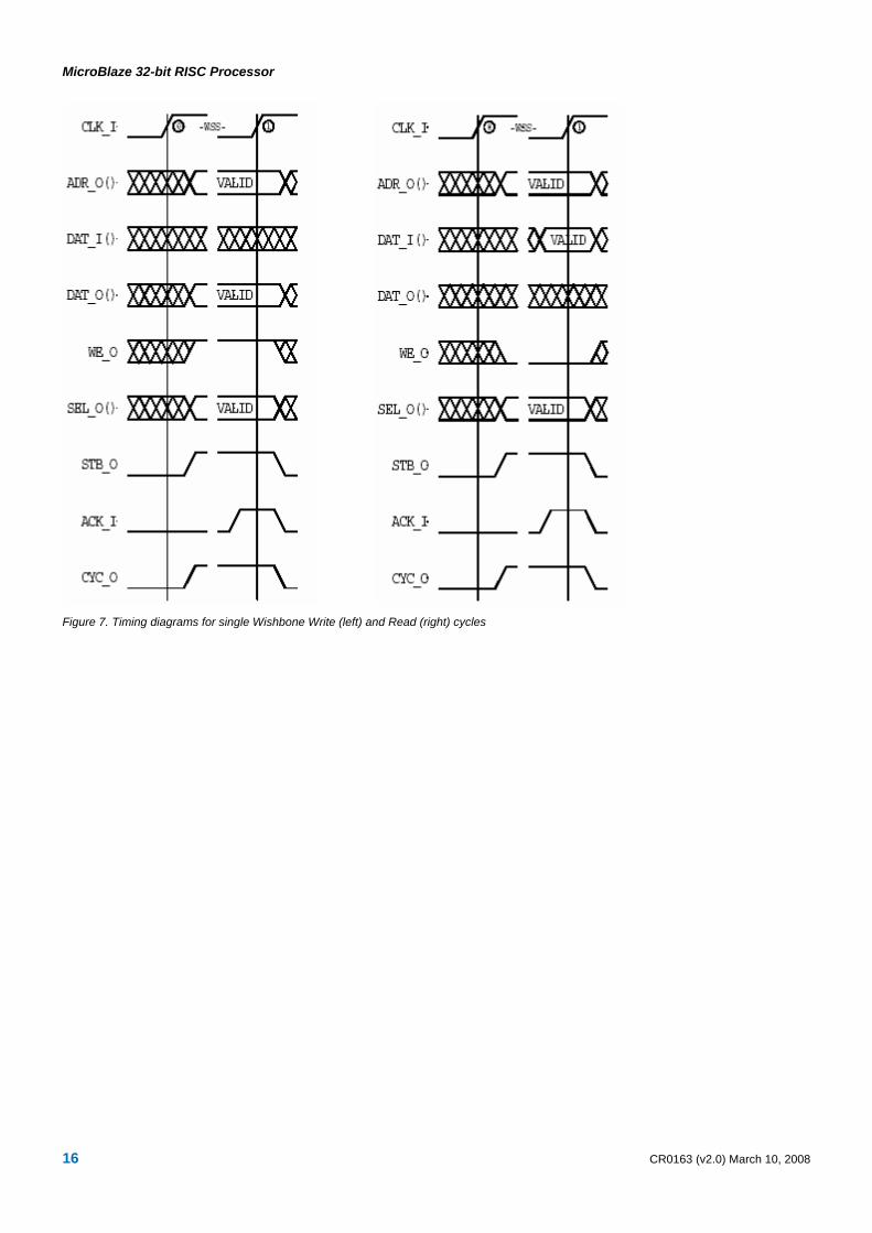
Wishbone Timing Figure 7 shows the signal timing for a standard single Wishbone Write Cycle (left) and Read Cycle (right), respectively. The timing diagrams are presented assuming point-to-point connection of the Master and Slave interfaces, with only signals on the Master side of the interface shown. Note that cycle speed can be throttled by the Slave device inserting wait states (represented as WSS on the diagrams) before asserting its acknowledgement line (ACK_I input at the Master side).
CR0163 (v2.0) March 10, 2008 15
MicroBlaze 32-bit RISC Processor
Figure 7. Timing diagrams for single Wishbone Write (left) and Read (right) cycles
16 CR0163 (v2.0) March 10, 2008
MicroBlaze 32-bit RISC Processor
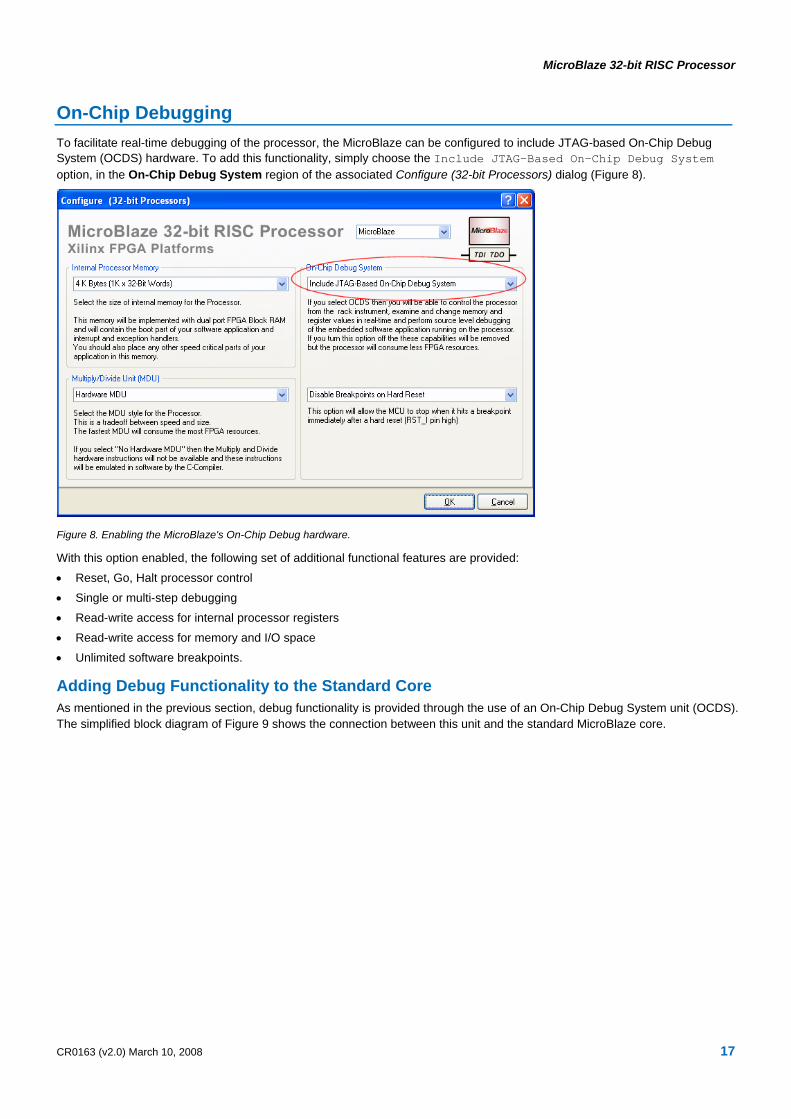
On-Chip Debugging To facilitate real-time debugging of the processor, the MicroBlaze can be configured to include JTAG-based On-Chip Debug System (OCDS) hardware. To add this functionality, simply choose the Include JTAG-Based On-Chip Debug System option, in the On-Chip Debug System region of the associated Configure (32-bit Processors) dialog (Figure 8).
Figure 8. Enabling the MicroBlaze's On-Chip Debug hardware.
With this option enabled, the following set of additional functional features are provided:
• Reset, Go, Halt processor control
• Single or multi-step debugging
• Read-write access for internal processor registers
• Read-write access for memory and I/O space
• Unlimited software breakpoints.
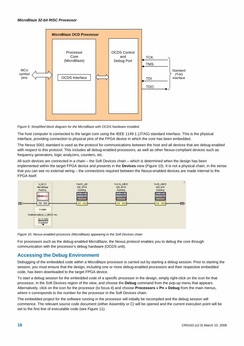
Adding Debug Functionality to the Standard Core As mentioned in the previous section, debug functionality is provided through the use of an On-Chip Debug System unit (OCDS). The simplified block diagram of Figure 9 shows the connection between this unit and the standard MicroBlaze core.
CR0163 (v2.0) March 10, 2008 17
MicroBlaze 32-bit RISC Processor
TCK
TMS
TDI
TDO
Standard JTAG
interface
MCU symbol
pins
MicroBlaze OCD Processor
Processor Core
(MicroBlaze)
OCDS Interface
OCDS Control and
Debug Port
Figure 9. Simplified block diagram for the MicroBlaze with OCDS hardware installed.
The host computer is connected to the target core using the IEEE 1149.1 (JTAG) standard interface. This is the physical interface, providing connection to physical pins of the FPGA device in which the core has been embedded.
The Nexus 5001 standard is used as the protocol for communications between the host and all devices that are debug-enabled with respect to this protocol. This includes all debug-enabled processors, as well as other Nexus-compliant devices such as frequency generators, logic analyzers, counters, etc.
All such devices are connected in a chain – the Soft Devices chain – which is determined when the design has been implemented within the target FPGA device and presents in the Devices view (Figure 10). It is not a physical chain, in the sense that you can see no external wiring – the connections required between the Nexus-enabled devices are made internal to the FPGA itself.
Figure 10. Nexus-enabled processor (MicroBlaze) appearing in the Soft Devices chain
For processors such as the debug-enabled MicroBlaze, the Nexus protocol enables you to debug the core through communication with the processor’s debug hardware (OCDS unit).
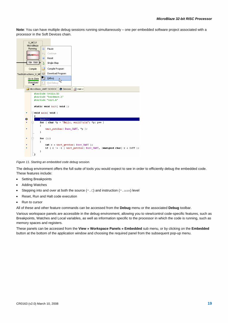
Accessing the Debug Environment Debugging of the embedded code within a MicroBlaze processor is carried out by starting a debug session. Prior to starting the session, you must ensure that the design, including one or more debug-enabled processors and their respective embedded code, has been downloaded to the target FPGA device.
To start a debug session for the embedded code of a specific processor in the design, simply right-click on the icon for that processor, in the Soft Devices region of the view, and choose the Debug command from the pop-up menu that appears. Alternatively, click on the icon for the processor (to focus it) and choose Processors » Pn » Debug from the main menus, where n corresponds to the number for the processor in the Soft Devices chain.
The embedded project for the software running in the processor will initially be recompiled and the debug session will commence. The relevant source code document (either Assembly or C) will be opened and the current execution point will be set to the first line of executable code (see Figure 11).
18 CR0163 (v2.0) March 10, 2008
MicroBlaze 32-bit RISC Processor
Note: You can have multiple debug sessions running simultaneously – one per embedded software project associated with a processor in the Soft Devices chain.
Figure 11. Starting an embedded code debug session.
The debug environment offers the full suite of tools you would expect to see in order to efficiently debug the embedded code. These features include:
• Setting Breakpoints
• Adding Watches • Stepping into and over at both the source (*.C) and instruction (*.asm) level
• Reset, Run and Halt code execution
• Run to cursor All of these and other feature commands can be accessed from the Debug menu or the associated Debug toolbar.
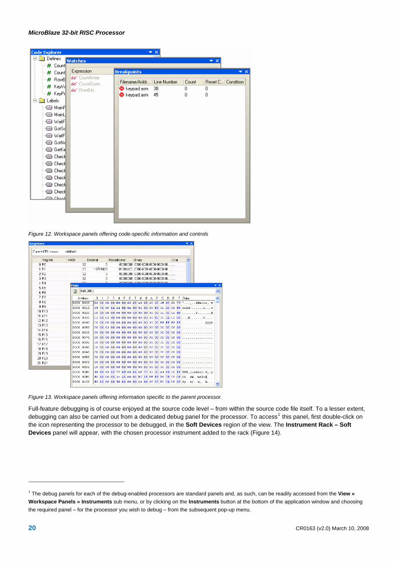
Various workspace panels are accessible in the debug environment, allowing you to view/control code-specific features, such as Breakpoints, Watches and Local variables, as well as information specific to the processor in which the code is running, such as memory spaces and registers. These panels can be accessed from the View » Workspace Panels » Embedded sub menu, or by clicking on the Embedded button at the bottom of the application window and choosing the required panel from the subsequent pop-up menu.
CR0163 (v2.0) March 10, 2008 19
MicroBlaze 32-bit RISC Processor
Figure 12. Workspace panels offering code-specific information and controls
Figure 13. Workspace panels offering information specific to the parent processor.
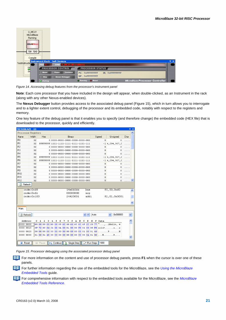
Full-feature debugging is of course enjoyed at the source code level – from within the source code file itself. To a lesser extent, debugging can also be carried out from a dedicated debug panel for the processor. To access1 this panel, first double-click on the icon representing the processor to be debugged, in the Soft Devices region of the view. The Instrument Rack – Soft Devices panel will appear, with the chosen processor instrument added to the rack (Figure 14).
1 The debug panels for each of the debug-enabled processors are standard panels and, as such, can be readily accessed from the View » Workspace Panels » Instruments sub menu, or by clicking on the Instruments button at the bottom of the application window and choosing the required panel – for the processor you wish to debug – from the subsequent pop-up menu.
20 CR0163 (v2.0) March 10, 2008
MicroBlaze 32-bit RISC Processor
Figure 14. Accessing debug features from the processor's instrument panel
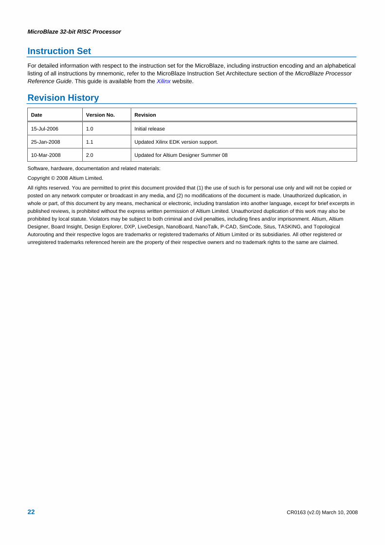
Note: Each core processor that you have included in the design will appear, when double-clicked, as an Instrument in the rack (along with any other Nexus-enabled devices). The Nexus Debugger button provides access to the associated debug panel (Figure 15), which in turn allows you to interrogate and to a lighter extent control, debugging of the processor and its embedded code, notably with respect to the registers and memory.
One key feature of the debug panel is that it enables you to specify (and therefore change) the embedded code (HEX file) that is downloaded to the processor, quickly and efficiently.
Figure 15. Processor debugging using the associated processor debug panel
For more information on the content and use of processor debug panels, press F1 when the cursor is over one of these panels.
For further information regarding the use of the embedded tools for the MicroBlaze, see the Using the MicroBlaze Embedded Tools guide.
For comprehensive information with respect to the embedded tools available for the MicroBlaze, see the MicroBlaze Embedded Tools Reference.
CR0163 (v2.0) March 10, 2008 21
MicroBlaze 32-bit RISC Processor
Instruction Set For detailed information with respect to the instruction set for the MicroBlaze, including instruction encoding and an alphabetical listing of all instructions by mnemonic, refer to the MicroBlaze Instruction Set Architecture section of the MicroBlaze Processor Reference Guide. This guide is available from the Xilinx website.
Revision History
Date Version No. Revision
15-Jul-2006 1.0 Initial release
25-Jan-2008 1.1 Updated Xilinx EDK version support.
10-Mar-2008 2.0 Updated for Altium Designer Summer 08
Software, hardware, documentation and related materials:
Copyright © 2008 Altium Limited.
All rights reserved. You are permitted to print this document provided that (1) the use of such is for personal use only and will not be copied or posted on any network computer or broadcast in any media, and (2) no modifications of the document is made. Unauthorized duplication, in whole or part, of this document by any means, mechanical or electronic, including translation into another language, except for brief excerpts in published reviews, is prohibited without the express written permission of Altium Limited. Unauthorized duplication of this work may also be prohibited by local statute. Violators may be subject to both criminal and civil penalties, including fines and/or imprisonment. Altium, Altium Designer, Board Insight, Design Explorer, DXP, LiveDesign, NanoBoard, NanoTalk, P-CAD, SimCode, Situs, TASKING, and Topological Autorouting and their respective logos are trademarks or registered trademarks of Altium Limited or its subsidiaries. All other registered or unregistered trademarks referenced herein are the property of their respective owners and no trademark rights to the same are claimed.
22 CR0163 (v2.0) March 10, 2008