Embed Size (px)
Citation preview
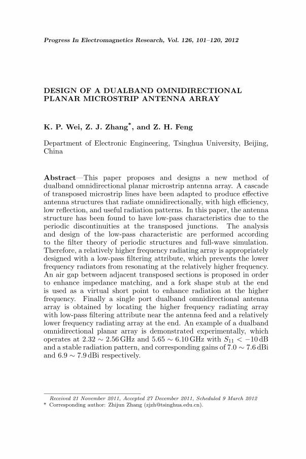
Progress In Electromagnetics Research, Vol. 126, 101–120, 2012
DESIGN OF A DUALBAND OMNIDIRECTIONALPLANAR MICROSTRIP ANTENNA ARRAY
K. P. Wei, Z. J. Zhang*, and Z. H. Feng
Department of Electronic Engineering, Tsinghua University, Beijing,China
Abstract—This paper proposes and designs a new method ofdualband omnidirectional planar microstrip antenna array. A cascadeof transposed microstrip lines have been adapted to produce effectiveantenna structures that radiate omnidirectionally, with high efficiency,low reflection, and useful radiation patterns. In this paper, the antennastructure has been found to have low-pass characteristics due to theperiodic discontinuities at the transposed junctions. The analysisand design of the low-pass characteristic are performed accordingto the filter theory of periodic structures and full-wave simulation.Therefore, a relatively higher frequency radiating array is appropriatelydesigned with a low-pass filtering attribute, which prevents the lowerfrequency radiators from resonating at the relatively higher frequency.An air gap between adjacent transposed sections is proposed in orderto enhance impedance matching, and a fork shape stub at the endis used as a virtual short point to enhance radiation at the higherfrequency. Finally a single port dualband omnidirectional antennaarray is obtained by locating the higher frequency radiating arraywith low-pass filtering attribute near the antenna feed and a relativelylower frequency radiating array at the end. An example of a dualbandomnidirectional planar array is demonstrated experimentally, whichoperates at 2.32 ∼ 2.56GHz and 5.65 ∼ 6.10GHz with S11 < −10 dBand a stable radiation pattern, and corresponding gains of 7.0 ∼ 7.6 dBiand 6.9 ∼ 7.9 dBi respectively.
Received 21 November 2011, Accepted 27 December 2011, Scheduled 9 March 2012* Corresponding author: Zhijun Zhang ([email protected]).
102 Wei, Zhang, and Feng
1. INTRODUCTION
Modern wireless communications systems typically require high-gainomnidirectional (in the azimuth plane) antennas to cover a large servicearea [1, 2]. In conventional applications, vertical dipole antennas witha half-wavelength resonant structure are the most popular choice.For many applications such as base stations or WLAN access-points(AP) [3–5], the half-wavelength dipole antenna has a gain of about2.15 dBi, which may not be sufficient. Moreover, the natural standingwave current distribution on the resonant long wire antenna producesone radiation lobe for each half-wavelength antenna section [6–8]. It isone of the oldest antennas, and has been studied for over a century.
Several phase-reversed antenna configurations immune to thisproblem have been proposed for high-directivity in the elevationplane. The collinear array (CoA) of dipole antennas is a well-knowncandidate for increasing the gain of a single dipole. The originalidea comes from Franklin [9]. He first designed CoA from a longwire that had λ/4 transverse narrow U-shaped sections to providea phase shift to maintain in-phase feeding of the straight λ/2 partsof the longitudinal radiating wire antenna. In this antenna, theU-shaped sections maintain in-phase currents along the longitudinalaxis, while the opposing and close transverse currents of the U-shaped sections cancel out to avoid cross-polar radiation. Basedon Franklin antenna’s concept, Wheeler designed an omnidirectionalCOCO (Colinear Coxial) antenna [10], made of a series of sectionsof solid-dielectric coaxial cable with their inner and outer conductorstransposed at each junction. Since each section has an effective lengthof nearly 0.5 wavelengths, the whole array of cables appear to bein the same phase. The cylindrical patch [11] used to be adoptedin order to solve the feeding problem, but the cost of constructingsuch a cylindrical array antenna is usually high, since the antennashad to conform to the cylindrical ground surface. Using a theorysimilar to that of the COCO antenna, Bancroft and Brennan furtherpresented various microstrip variations [12–14] of the COCO antenna.These omnidirectional antennas have the advantages of planarity, easyintegration and low construction costs, compared to coaxial antennas.
Due to the rapid development of mobile communications, the needfor omnidirectional antennas with multi-band operation has increasedconsiderably [15–17]. For instance, wireless local area network(WLAN) operates at both 2.4 to 2.5 GHz (IEEE 802.11b and IEEE802.11g) and 5.15 to 5.875GHz (IEEE 802.11a) frequency bands [18–20]. To integrate both bands into one device, for simple systemconfiguration and cost reduction, it is important to develop dualband
Progress In Electromagnetics Research, Vol. 126, 2012 103
omnidirectional antennas with high directivity. Unfortunately, sincethe existing series-fed omnidirectional planar antennas needed a 180phase shift to excite all radiating elements in phase, the distancebetween adjacent sections should be a half-wavelength. The traditionalomnidirectional planar antenna array typically has 2% of impedancebandwidth and 2.3% of pattern bandwidth [12]. Therefore, designinga dualband planar omnidirectional antenna with narrow beams isstill a significant challenge. Existing dual omnidirectional planarantenna arrays [18–20] could not control the radiation aperture, andhave problems with small limited gain due to the shunt-fed network.Recently, the integration of dualband antennas based on two elementsand bandpass filters has been considered to be one of the best solutionsfor dual or multiband systems, which can be used for the suppressionof unwanted harmonics of the antenna and in the improvement ofreflection loss and the selectivity of the antenna [21–25]. Therefore,we propose a novel design method of the dualband omnidirectionalplanar microstrip antenna array. Using the methods based on filtertheory, the radiation aperture of the dualband array can be controlled,allowing both lower frequency and higher frequency radiators to co-exist and operate independently.
2. DESIGN METHODOLOGY
The omnidirectional (in the azimuth plane) antenna arrays are moredifficult to design compared to directional antenna arrays, because thatthe feeding networks should be strictly arranged with no distortionof omnidirectional patterns. Since the feeding networks reciprocallydisturb the omnidirectional patterns, omnidrectional arrays operatingat different bands that are mounted independently with discrete portsare unworkable. Therefore, a dualband omnidiretional antenna arraywith stable omnidirectional radiation pattern is preferred due to itssimple system configuration and potential for cost reduction. Theexisting dualband omnidiretional planar element has been achievedby employing different modes of chamfered dipoles [18–20], whichcould not be readily arranged to form an array with a controlledradiation aperture. The major aim of this paper is to provide a methodfor designing a dualband omnidirectional planar antenna array withcontrolled radiation aperture.
Omnidirectional antenna arrays with high gain are usuallycollinear arrays (CoA), which are based on the in-phase feedingof radiating elements that lie in a straight line. The majoradvantages of this collinear arrangement is that it results in muchlower coupling between elements and has a typically omnidirectional
104 Wei, Zhang, and Feng
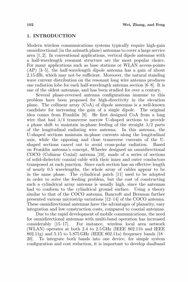
radiation without degradation caused by the feeding network. Dueto the shunt-fed configuration being limited by the element numbersand complex feeding network, a collinear series-fed configuration ischosen in this paper. In order to avoid disturbing the omnidirectionalradiation patterns by the feeding networks, the single port dualbandomnidirectional antenna array shown in Fig. 1 is obtained by locatingthe higher frequency radiating array with low-pass filtering attributesnear the antenna feed, and a relatively lower frequency radiating arrayat the end. To meet the requirements of IEEE 802.11a/b/g wirelesslocal area network (WLAN), a 2.4/5.8-GHz dualband omnidirectionalplanar antenna array is presented as an example.
As mentioned above, the major issue regarding the design is thearrangement of the feeding network and the isolation between the2.4GHz radiator and 5.8 GHz radiator for the suppression of unwantedradiation patterns. For allowing both the 2.4 GHz array and 5.8 GHzarray to co-exist and operate independently with controlled radiationapertures, the idea of a microwave filter is applied in this structure.The 5.8GHz array near the antenna feed is also designed as a microstripfilter with low-pass characteristics at the 2.4 GHz frequency band. Thelow-pass filtering attribute is used to prevent the 5.8 GHz radiator fromresonating at the 2.4 GHz frequency band. This transmits power atthe 2.4 GHz frequency band to the 2.4 GHz array at the end. Sincethe 5.8 GHz high-order mode resonates on the 2.4 GHz array, whichwill result in unwanted radiation patterns. As a result, the 5.8GHzsignal should mostly be radiated by the 5.8GHz array. Therefore,the radiation of the 5.8GHz signal at the 5.8GHz radiator should beenhanced.
A series-fed planar antenna array made of a cascade of transposedmicrostrip line sections has been proposed in [12], which is one of thebest solutions to produce an omnidirectional radiation pattern withhigh directivity. In this paper, periodically transposed microstrip lineshave also been found to allow a low-pass characteristic due to theperiodic discontinuities at transposed junctions. The analysis and
Figure 1. Schematic of the proposed single port dualbandomnidirectional antenna array.
Progress In Electromagnetics Research, Vol. 126, 2012 105
design of the low-pass characteristic are performed according to thefilter theory of periodic structures explained in the next section.
3. LOW-PASS FILTERING ATTRIBUTES OFPERIODICALLY TRANSPOSED MICROSTRIP LINES
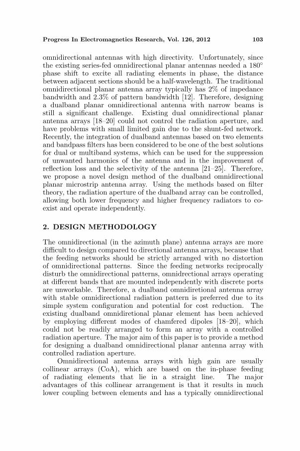
Figure 2 shows the overall configuration of periodically transposedmicrostrip lines. The structure is composed of a plurality of microstriptransmission line sections, periodically transposed at each junctionwith a period of d. The microstrip transmission line in this structureconsists of two strip conductors of width w1 and width w2, which areseparated by a dielectric material of permittivity εr and thicknessh. All the microstrip transmission line sections have the samecharacteristic impedance of Zc. Since the (n− 1)th and nth microstriptransmission line sections are reversed, with the same dimensions, thesmall difference can be neglected in practice, so that the period of thestructure can be considered to be equal to d.
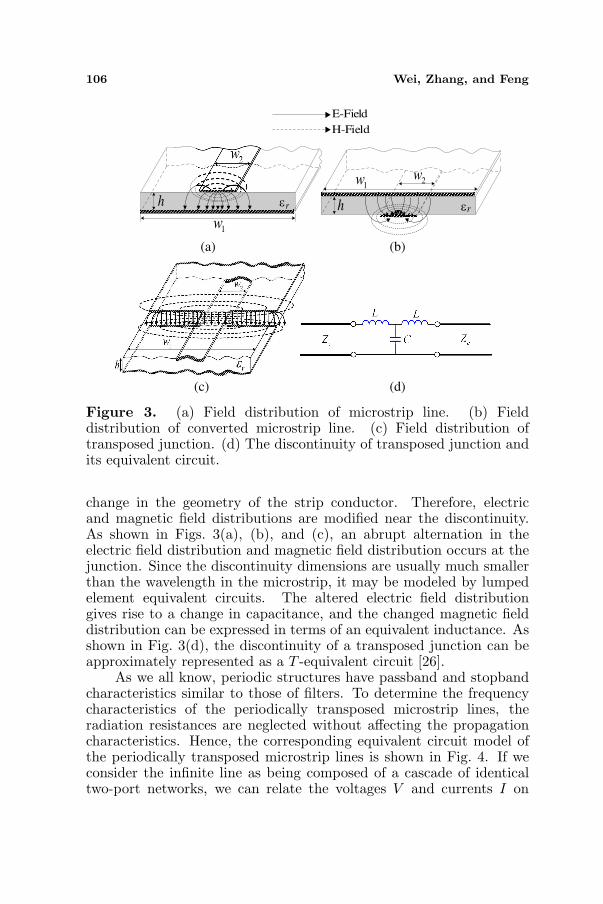
As we can see, a transposed microstrip line section can beconsidered as a junction between a microstrip line and a convertedmicrostrip line. Figs. 3(a), (b), and (c) show the electric and magneticfield distributions of the microstrip line, converted microstrip lineand the transposed microstrip line sections respectively. It is clearthat a discontinuity in a transposed junction is caused by an abrupt
Figure 2. Overall configuration of periodically transposed microstripline sections.
106 Wei, Zhang, and Feng
E-Field
H-Field
h r
1w
rh
2w
2w
1w
εε
(a)
(c)
(b)
(d)
Figure 3. (a) Field distribution of microstrip line. (b) Fielddistribution of converted microstrip line. (c) Field distribution oftransposed junction. (d) The discontinuity of transposed junction andits equivalent circuit.
change in the geometry of the strip conductor. Therefore, electricand magnetic field distributions are modified near the discontinuity.As shown in Figs. 3(a), (b), and (c), an abrupt alternation in theelectric field distribution and magnetic field distribution occurs at thejunction. Since the discontinuity dimensions are usually much smallerthan the wavelength in the microstrip, it may be modeled by lumpedelement equivalent circuits. The altered electric field distributiongives rise to a change in capacitance, and the changed magnetic fielddistribution can be expressed in terms of an equivalent inductance. Asshown in Fig. 3(d), the discontinuity of a transposed junction can beapproximately represented as a T -equivalent circuit [26].
As we all know, periodic structures have passband and stopbandcharacteristics similar to those of filters. To determine the frequencycharacteristics of the periodically transposed microstrip lines, theradiation resistances are neglected without affecting the propagationcharacteristics. Hence, the corresponding equivalent circuit model ofthe periodically transposed microstrip lines is shown in Fig. 4. If weconsider the infinite line as being composed of a cascade of identicaltwo-port networks, we can relate the voltages V and currents I on
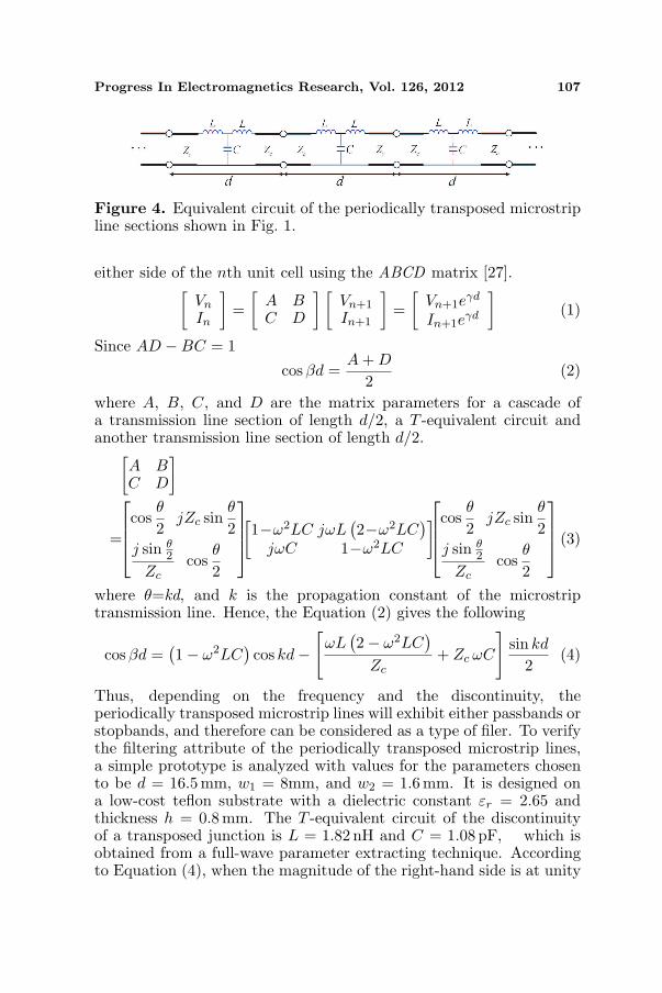
Progress In Electromagnetics Research, Vol. 126, 2012 107
Figure 4. Equivalent circuit of the periodically transposed microstripline sections shown in Fig. 1.
either side of the nth unit cell using the ABCD matrix [27].[
Vn
In
]=
[A BC D
] [Vn+1
In+1
]=
[Vn+1e
γd
In+1eγd
](1)
Since AD −BC = 1
cosβd =A + D
2(2)
where A, B, C, and D are the matrix parameters for a cascade ofa transmission line section of length d/2, a T -equivalent circuit andanother transmission line section of length d/2.
[A BC D
]
=
cosθ
2jZc sin
θ
2j sin θ
2
Zccos
θ
2
[1−ω2LC jωL
(2−ω2LC
)jωC 1−ω2LC
]
cosθ
2jZc sin
θ
2j sin θ
2
Zccos
θ
2
(3)
where θ=kd, and k is the propagation constant of the microstriptransmission line. Hence, the Equation (2) gives the following
cosβd =(1− ω2LC
)cos kd−
[ωL
(2− ω2LC
)
Zc+ Zc ωC
]sin kd
2(4)
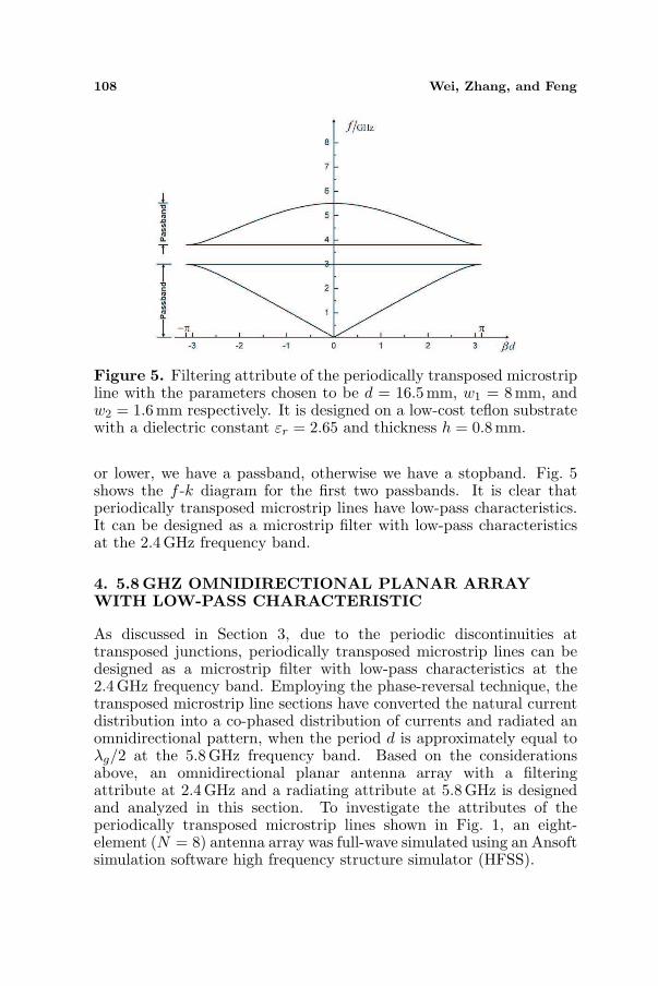
Thus, depending on the frequency and the discontinuity, theperiodically transposed microstrip lines will exhibit either passbands orstopbands, and therefore can be considered as a type of filer. To verifythe filtering attribute of the periodically transposed microstrip lines,a simple prototype is analyzed with values for the parameters chosento be d = 16.5mm, w1 = 8mm, and w2 = 1.6mm. It is designed ona low-cost teflon substrate with a dielectric constant εr = 2.65 andthickness h = 0.8mm. The T -equivalent circuit of the discontinuityof a transposed junction is L = 1.82 nH and C = 1.08 pF, which isobtained from a full-wave parameter extracting technique. Accordingto Equation (4), when the magnitude of the right-hand side is at unity
108 Wei, Zhang, and Feng
Figure 5. Filtering attribute of the periodically transposed microstripline with the parameters chosen to be d = 16.5mm, w1 = 8mm, andw2 = 1.6mm respectively. It is designed on a low-cost teflon substratewith a dielectric constant εr = 2.65 and thickness h = 0.8mm.
or lower, we have a passband, otherwise we have a stopband. Fig. 5shows the f -k diagram for the first two passbands. It is clear thatperiodically transposed microstrip lines have low-pass characteristics.It can be designed as a microstrip filter with low-pass characteristicsat the 2.4GHz frequency band.
4. 5.8 GHZ OMNIDIRECTIONAL PLANAR ARRAYWITH LOW-PASS CHARACTERISTIC
As discussed in Section 3, due to the periodic discontinuities attransposed junctions, periodically transposed microstrip lines can bedesigned as a microstrip filter with low-pass characteristics at the2.4GHz frequency band. Employing the phase-reversal technique, thetransposed microstrip line sections have converted the natural currentdistribution into a co-phased distribution of currents and radiated anomnidirectional pattern, when the period d is approximately equal toλg/2 at the 5.8 GHz frequency band. Based on the considerationsabove, an omnidirectional planar antenna array with a filteringattribute at 2.4GHz and a radiating attribute at 5.8 GHz is designedand analyzed in this section. To investigate the attributes of theperiodically transposed microstrip lines shown in Fig. 1, an eight-element (N = 8) antenna array was full-wave simulated using an Ansoftsimulation software high frequency structure simulator (HFSS).
Progress In Electromagnetics Research, Vol. 126, 2012 109
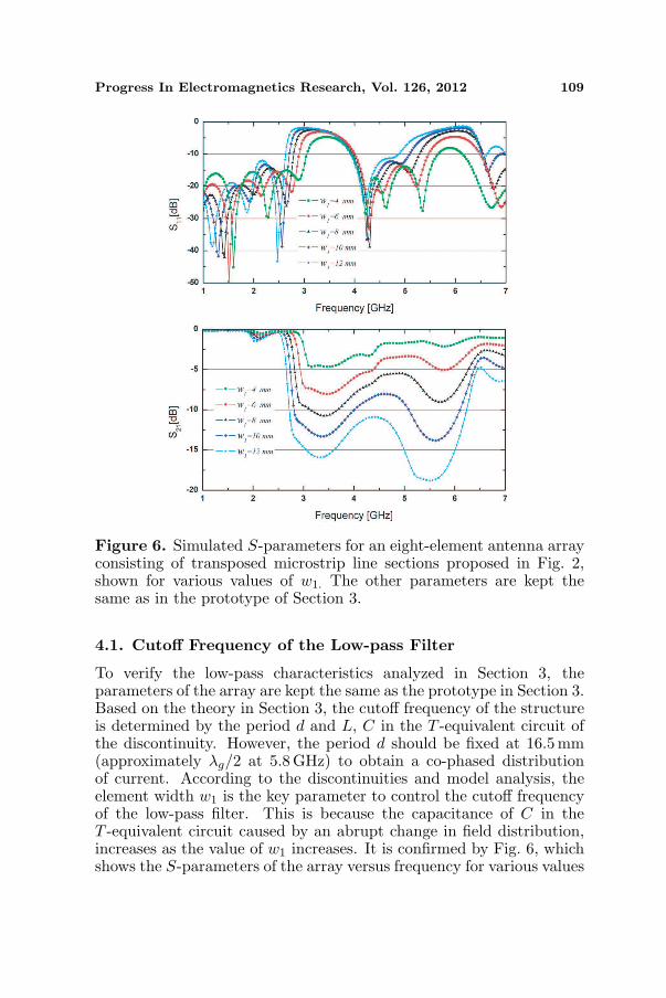
Figure 6. Simulated S-parameters for an eight-element antenna arrayconsisting of transposed microstrip line sections proposed in Fig. 2,shown for various values of w1. The other parameters are kept thesame as in the prototype of Section 3.
4.1. Cutoff Frequency of the Low-pass Filter
To verify the low-pass characteristics analyzed in Section 3, theparameters of the array are kept the same as the prototype in Section 3.Based on the theory in Section 3, the cutoff frequency of the structureis determined by the period d and L, C in the T -equivalent circuit ofthe discontinuity. However, the period d should be fixed at 16.5 mm(approximately λg/2 at 5.8 GHz) to obtain a co-phased distributionof current. According to the discontinuities and model analysis, theelement width w1 is the key parameter to control the cutoff frequencyof the low-pass filter. This is because the capacitance of C in theT -equivalent circuit caused by an abrupt change in field distribution,increases as the value of w1 increases. It is confirmed by Fig. 6, whichshows the S-parameters of the array versus frequency for various values
110 Wei, Zhang, and Feng
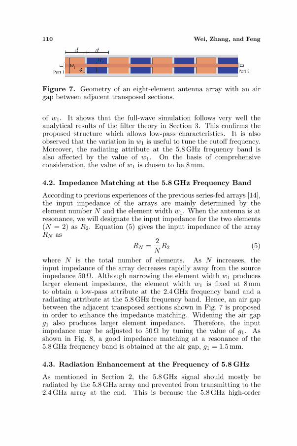
Figure 7. Geometry of an eight-element antenna array with an airgap between adjacent transposed sections.
of w1. It shows that the full-wave simulation follows very well theanalytical results of the filter theory in Section 3. This confirms theproposed structure which allows low-pass characteristics. It is alsoobserved that the variation in w1 is useful to tune the cutoff frequency.Moreover, the radiating attribute at the 5.8 GHz frequency band isalso affected by the value of w1. On the basis of comprehensiveconsideration, the value of w1 is chosen to be 8 mm.
4.2. Impedance Matching at the 5.8 GHz Frequency Band
According to previous experiences of the previous series-fed arrays [14],the input impedance of the arrays are mainly determined by theelement number N and the element width w1. When the antenna is atresonance, we will designate the input impedance for the two elements(N = 2) as R2. Equation (5) gives the input impedance of the arrayRN as
RN =2N
R2 (5)
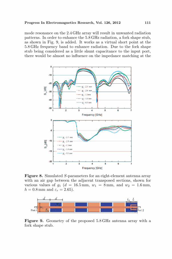
where N is the total number of elements. As N increases, theinput impedance of the array decreases rapidly away from the sourceimpedance 50 Ω. Although narrowing the element width w1 produceslarger element impedance, the element width w1 is fixed at 8 mmto obtain a low-pass attribute at the 2.4 GHz frequency band and aradiating attribute at the 5.8 GHz frequency band. Hence, an air gapbetween the adjacent transposed sections shown in Fig. 7 is proposedin order to enhance the impedance matching. Widening the air gapg1 also produces larger element impedance. Therefore, the inputimpedance may be adjusted to 50Ω by tuning the value of g1. Asshown in Fig. 8, a good impedance matching at a resonance of the5.8GHz frequency band is obtained at the air gap, g1 = 1.5mm.
4.3. Radiation Enhancement at the Frequency of 5.8 GHz
As mentioned in Section 2, the 5.8GHz signal should mostly beradiated by the 5.8GHz array and prevented from transmitting to the2.4GHz array at the end. This is because the 5.8 GHz high-order
Progress In Electromagnetics Research, Vol. 126, 2012 111
mode resonance on the 2.4 GHz array will result in unwanted radiationpatterns. In order to enhance the 5.8 GHz radiation, a fork shape stub,as shown in Fig. 9, is added. It works as a virtual short point at the5.8GHz frequency band to enhance radiation. Due to the fork shapestub being considered as a little shunt capacitance to the input port,there would be almost no influence on the impedance matching at the
Figure 8. Simulated S-parameters for an eight-element antenna arraywith an air gap between the adjacent transposed sections, shown forvarious values of g1 (d = 16.5mm, w1 = 8mm, and w2 = 1.6mm,h = 0.8mm and εr = 2.65).
Figure 9. Geometry of the proposed 5.8GHz antenna array with afork shape stub.
112 Wei, Zhang, and Feng
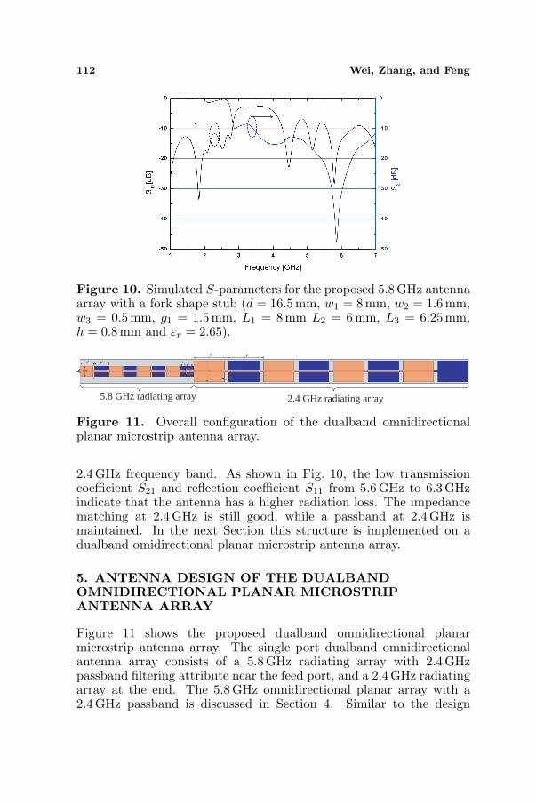
Figure 10. Simulated S-parameters for the proposed 5.8 GHz antennaarray with a fork shape stub (d = 16.5mm, w1 = 8 mm, w2 = 1.6mm,w3 = 0.5mm, g1 = 1.5mm, L1 = 8 mm L2 = 6 mm, L3 = 6.25mm,h = 0.8mm and εr = 2.65).
2.4 GHz radiating array5.8 GHz radiating array
Figure 11. Overall configuration of the dualband omnidirectionalplanar microstrip antenna array.
2.4GHz frequency band. As shown in Fig. 10, the low transmissioncoefficient S21 and reflection coefficient S11 from 5.6 GHz to 6.3 GHzindicate that the antenna has a higher radiation loss. The impedancematching at 2.4 GHz is still good, while a passband at 2.4GHz ismaintained. In the next Section this structure is implemented on adualband omidirectional planar microstrip antenna array.
5. ANTENNA DESIGN OF THE DUALBANDOMNIDIRECTIONAL PLANAR MICROSTRIPANTENNA ARRAY
Figure 11 shows the proposed dualband omnidirectional planarmicrostrip antenna array. The single port dualband omnidirectionalantenna array consists of a 5.8 GHz radiating array with 2.4 GHzpassband filtering attribute near the feed port, and a 2.4 GHz radiatingarray at the end. The 5.8 GHz omnidirectional planar array with a2.4GHz passband is discussed in Section 4. Similar to the design
Progress In Electromagnetics Research, Vol. 126, 2012 113
of the 5.8 GHz radiating array, the 2.4GHz omnidirectional planararray is achieved by designing the period p as being approximatelyequal to λg/2 at the 2.4 GHz frequency band. Optimized impedancematching at the 2.4 GHz frequency band can be obtained by adjustingthe parameters of g2, w4 and w5. The dualband omnidirectionalplanar microstrip antenna array shown in Fig. 11 was designed andsimulated using Ansoft’s HFSS full-wave simulator. The final designof the dualband omnidirectional array has the following parameters:d = 16.5mm, p = 40 mm, w1 = 8mm, w2 = 1.6mm, w3 = 0.5mm,w4 = 16 mm, w5 = 1.2 mm, g1 = 1.5mm, g2 = 5 mm, L1 = 8 mm,L2 = 6 mm and L3 = 6.25mm. The substrate of the proposed antennaarray is low-cost telfon with a dielectric constant εr = 2.65 and athickness h = 0.8 mm. The geometry of the overall antenna array is445.5× 20× 0.8 mm3.
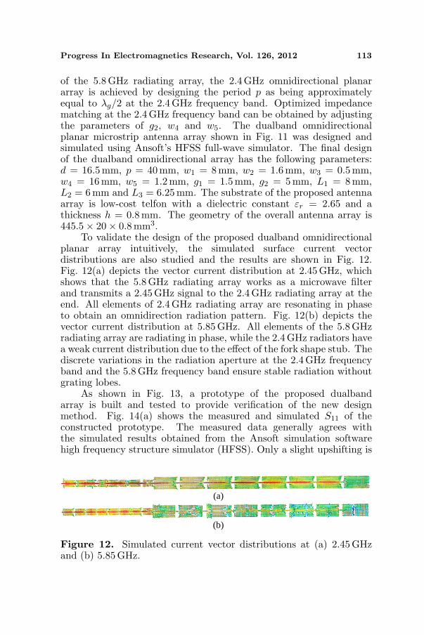
To validate the design of the proposed dualband omnidirectionalplanar array intuitively, the simulated surface current vectordistributions are also studied and the results are shown in Fig. 12.Fig. 12(a) depicts the vector current distribution at 2.45 GHz, whichshows that the 5.8GHz radiating array works as a microwave filterand transmits a 2.45 GHz signal to the 2.4 GHz radiating array at theend. All elements of 2.4 GHz radiating array are resonating in phaseto obtain an omnidirection radiation pattern. Fig. 12(b) depicts thevector current distribution at 5.85 GHz. All elements of the 5.8GHzradiating array are radiating in phase, while the 2.4GHz radiators havea weak current distribution due to the effect of the fork shape stub. Thediscrete variations in the radiation aperture at the 2.4 GHz frequencyband and the 5.8GHz frequency band ensure stable radiation withoutgrating lobes.
As shown in Fig. 13, a prototype of the proposed dualbandarray is built and tested to provide verification of the new designmethod. Fig. 14(a) shows the measured and simulated S11 of theconstructed prototype. The measured data generally agrees withthe simulated results obtained from the Ansoft simulation softwarehigh frequency structure simulator (HFSS). Only a slight upshifting is
(a)
(b)
Figure 12. Simulated current vector distributions at (a) 2.45 GHzand (b) 5.85GHz.
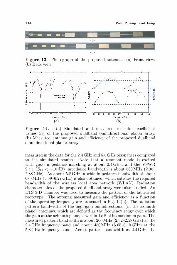
114 Wei, Zhang, and Feng
(a)
(b)
Figure 13. Photograph of the proposed antenna. (a) Front view.(b) Back view.
(a) (b)
Figure 14. (a) Simulated and measured reflection coefficientvalues S11 of the proposed dualband omnidirectional planar array.(b) Measured antenna gain and efficiency of the proposed dualbandomnidirectional planar array.
measured in the data for the 2.4GHz and 5.8 GHz resonances comparedto the simulated results. Note that a resonant mode is excitedwith good impedance matching at about 2.4 GHz, and the VSWR2 : 1 (S11 < −10 dB) impedance bandwidth is about 580MHz (2.30–2.88GHz). At about 5.8 GHz, a wide impedance bandwidth of about680MHz (5.59–6.27 GHz) is also obtained, which satisfies the requiredbandwidth of the wireless local area network (WLAN). Radiationcharacteristics of the proposed dualband array were also studied. AnETS 3-D chamber was used to measure the pattern of the fabricatedprototype. The antenna measured gain and efficiency as a functionof the operating frequency are presented in Fig. 14(b). The radiationpattern bandwidth of the high-gain omnidirectional (in the azimuthplane) antennas, which are defined as the frequency range over whichthe gain at the azimuth plane, is within 1 dB of its maximum gain. Themeasured pattern bandwidth is about 260 MHz (2.32–2.58 GHz) at the2.4GHz frequency band and about 450 MHz (5.65–6.10 GHz) at the5.8GHz frequency band. Across pattern bandwidth at 2.4 GHz, the

Progress In Electromagnetics Research, Vol. 126, 2012 115
(a)
(b)
(c)
Figure 15. Measured normalized radiation patterns of the fabricatedprototype in the pattern bandwidth at the 2.4 GHz frequency band.(a) f = 2320 MHz. (b) f = 2450 MHz. (c) f = 2580 MHz.
116 Wei, Zhang, and Feng
(a)
(b)
(c)
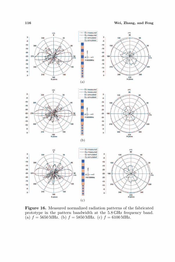
Figure 16. Measured normalized radiation patterns of the fabricatedprototype in the pattern bandwidth at the 5.8 GHz frequency band.(a) f = 5650 MHz. (b) f = 5850 MHz. (c) f = 6100 MHz.
Progress In Electromagnetics Research, Vol. 126, 2012 117
measured antenna gain is in a range of about 7.0 ∼ 7.6 dBi. At about5.8GHz, the measured antenna gain is 6.9 ∼ 7.9 dBi. It is clear that theradiation aperture of the dualband array is controlled. The ETS 3-Dchamber can also provide an estimated value of the radiation efficiencyof the measured antenna. The efficiency is defined as the ratio ofradiated power versus the total available from the power source. Thusthe efficiency value includes all impacts from mismatch loss, dielectricloss, conductor loss and matching component loss. The efficiency ofthe planar dipole array antenna varies from 87% to 93% in the patternbandwidth at the 2.4 GHz frequency band, while it varies between 84%to 95% at the 5.8 GHz frequency band.
The measured normalized radiation patterns of the fabricatedprototype in the pattern bandwidth at the 2.4 GHz frequency band areshown in Fig. 15. Only three representative frequencies (f = 2.32 GHz,f = 2.45GHz and f = 2.58GHz) are presented. Measurements atother operating frequencies across the 2.4 GHz band (not shown herefor brevity) also show similar radiation patterns as those plotted here,which indicates that the radiation patterns are stable in the desiredoperating band. The measured normalized E-plane pattern and H-plane pattern of the fabricated prototype in the pattern bandwidthat the 2.4 GHz frequency band are also presented in Fig. 16. Ascan be seen from all the radiation patterns, the main beam isapproximately fixed at broadside. From these results, it is clear thatgood omnidirectional radiation with vertical polarization in the H-plane (x-y plane) with a small gain variation of less than 1.5 dBiis obtained. In the E-plane (x-z plane), the HBPW (half-powerbeamwidth) of the proposed dualband planar array is about 19 at2.45GHz and 18 at 5.85 GHz.
6. CONCLUSION
A novel dualband omnidirectional planar microstrip antenna arraywith stable radiation pattern and gain has been studied and designed.In contrast with previous planar dualband antennas, this methodologyfor designing a higher frequency radiating array with a low-passfiltering attribute has been used to prevent the relatively lowerfrequency radiators from resonating at higher frequencies. Usinga method based on filter theory, the radiation aperture of thedualband array is controlled, allowing both lower frequency andhigher frequency radiators to co-exist and operate independently. Acascade of transposed sections of planar microstrip has been design toradiate at a higher frequency with a low-pass filtering attribute. Theanalysis and explanation of the low-pass characteristic are performed

118 Wei, Zhang, and Feng
according to the filter theory of periodic structures and by full-wave simulation. Finally, a single port dualband omnidirectionalantenna array is obtained by locating the higher frequency radiatingarray with the low-pass filtering attribute near the antenna feedand a relatively lower frequency radiating array at the end. Tomeet the requirements of the IEEE 802.11a/b/g wireless local areanetwork (WLAN), a simple prototype follows the design that has beendemonstrated experimentally, which operates at 2.32 ∼ 2.56GHz and5.65 ∼ 6.10GHz with S11 < −10 dB and a stable radiation pattern,and with corresponding gains of 7.0 ∼ 7.6 dBi and 6.9 ∼ 7.9 dBirespectively. Good vertically polarized omnidirectional radiation in theH-plane (x-y plane) with a small gain variation of less than 1.5 dBi isobtained.
ACKNOWLEDGMENT
This work is supported by the National Basic Research Program ofChina under Contract 2010CB327400, in part by the National NaturalScience Foundation of China under Contract 60771009, the NationalHigh Technology Research and Development Program of China (863Program) under Contract 2009AA011503, the National Science andTechnology Major Project of the Ministry of Science and Technologyof China 2010ZX03007-001-01, and Tsinghua-QUALCOMM associatedResearch Plan.
REFERENCES
1. Li, J. Y., J. L. Guo, Y. B. Gan, and Q. Z. Liu, “The tri-bandperformance of sleeve dipole antenna,” Journal of ElectromagneticWaves and Applications, Vol. 19, No. 15, 2081–2092, 2005.
2. Khaleghi, A., “Diversity techniques with parallel dipole anten-nas: Radiation pattern analysis,” Progress In ElectromagneticsResearch, Vol. 64, 23–42, 2006.
3. Zaker, R., C. Ghobadi, and J. Nourinia, “A modified microstrip-FED two-step tapered monopole antenna for UWB and WLANapplications,” Progress In Electromagnetics Research, Vol. 77,137–148, 2007.
4. Jaw, J.-L., F.-S. Chen, and D.-F. Chen, “Compact dualbandCPW-fed slotted patch antenna for 2.4/5 GHz WLAN operation,”Journal of Electromagnetic Waves and Applications, Vol. 23,No. 14–15, 1947–1955, 2009.
Progress In Electromagnetics Research, Vol. 126, 2012 119
5. Panda, J. R. and R. S. Kshetrimayum, “A printed2.4GHz/5.8 GHz dual-band monopole antenna with a protrudingstub in the ground plane for WLAN and RFID applications,”Progress In Electromagnetics Research, Vol. 117, 425–434, 2011.
6. Franklin, C. S., “Improvements in wireless telegraph andtelephone aerials,” British Patent, No. 242, 342, 1924.
7. Ghosh, S., A. Chakraborty, and S. Sanyal, “Loaded wire antennaas EMI sensor,” Progress In Electromagnetics Research, Vol. 54,19–36, 2005.
8. Poljak, D. and V. Doric, “Wire antenna model for transientanalysis of simple grounding systems. Part I: The verticalgrounding electrode,” Progress In Electromagnetics Research,Vol. 64, 149–166, 2006.
9. Solbach, K., “Microstrip-franklin antenna,” IEEE Trans. Anten-nas Propagat., Vol. 30, No. 4, 773–775, 1982.
10. Judasz, T. J. and B. B. Balsley, “Improved theoretical andexperimental models for the coaxial colinear antenna,” IEEETrans. Antennas Propagat., Vol. 37, 289–296, 1989.
11. Herscovici, N., Z. Sipus, and P.-S. Kildal, “The cylindrical om-nidirectional patch antenna,” IEEE Trans. Antennas Propagat.,Vol. 49, 1746–1753, Dec. 2001.
12. Bancroft, R. and B. Bateman, “An omnidirectional microstripantenna,” IEEE Trans. Antennas Propagat., Vol. 52, 3151–3153,Nov. 2004.
13. Bancroft, R. and B. Bateman, “An omnidirectional planarmicrostrip antenna with low sidelobes,” Microwave and OpticalTechnology Letters, Vol. 42, 68–69, Jul. 2004.
14. Bancroft, R., “Design parameters of an omnidirectional planarmicrostrip antenna,” Microwave and Optical Technology Letters,Vol. 47, No. 5, 414–418, Dec. 2005.
15. Li, J.-Y. and Y.-B. Gan, “Multi-band characteristic of open sleeveantenna,” Progress In Electromagnetics Research, Vol. 58, 135–148, 2006.
16. Wei, K., Z. Zhang, W. Chen, and Z. Fengm, and M. F. Iskander,“A triband shunt-fed omnidirectional planar dipole array,” IEEEAntennas Wireless Propag. Lett, Vol. 9, 850–85, 2010.
17. Alkanhal, M. A. S., “Composite compact triple-band microstripantennas,” Progress In Electromagnetics Research, Vol. 93, 221–236, 2009.
18. Tze-Meng, O., K. G. Tan, and A. W. Reza, “A dual-band omni-directional microstrip antenna,” Progress In Electromagnetics
120 Wei, Zhang, and Feng
Research, Vol. 106, 363–376, 2010.19. Si, L.-M. and X. Lv, “CPW-FED multi-band omni-directional pla-
nar microstrip antenna using composite metamaterial resonatorsfor wireless communications,” Progress In Electromagnetics Re-search, Vol. 83, 133–146, 2008.
20. Wu, Y.-J., B.-H. Sun, J.-F. Li, and Q.-Z. Liu, “Triple-bandomni-directional antenna for WLAN application,” Progress InElectromagnetics Research, Vol. 76, 477–484, 2007.
21. Shum, Y. H., K. M. Luk, and C. H. Chan, “Multi-band basestation antenna with compact microstrip resonant cell filters,” IEEProc. - Microw. Antennas Propag., Vol. 151, No. 6, 2004.
22. Suh, Y. H. and K. Chang, “A high-efficiency dual-frequencyrectenna for 2.45-and 5.8-GHz wireless power transmission,” IEEETrans. Microwave Theory Tech., Vol. 50, No. 7, 2002.
23. Barbarino, S. and F. Consoli, “UWB circular slot antennaprovided with an inverted-l notch filter for the 5GHz WLANband,” Progress In Electromagnetics Research, Vol. 104, 1–13,2010.
24. Toh, W. K., X. M. Qing, and Z. N. Chen, “A planar dualbandantenna array,” IEEE Trans. Antennas Propagat., Vol. 59, No. 3,833–838, Mar. 2011.
25. Isom, R., M. F. Iskander, Z. Yun, and Z. Zhang, “Designand development of multiband coaxial continuous transerse stub(CTS) antenna arrays,” IEEE Trans. Antennas Propagat., Vol. 52,No. 8, Aug. 2004.
26. Gupta, K. C., R. Garg, and I. J. Bahl, Microstrip Lines andSlotlines, Artech House, Dedham, Mass., 1979.
27. Pozar, D. M., Microwave Engineering, 3rd edition, John Wiley &Sons, Inc., New York, 2005.