Embed Size (px)
Citation preview
DESIGN OF A FULLY DIGITAL MULTI-LEVEL DECISION
FEEDBACK EQUALIZATION CHIP
XIE JIANG
(B.Eng(Hons.), BUPT)
A THESIS SUBMITTED
FOR THE DEGREE OF MASTER OF ENGINEERING
DEPARTMENT OF ELECTRICAL & COMPUTER ENGINEERING
NATIONAL UNIVERSITY OF SINGAPORE
2004
i
ACKNOWLEDGMENT
I would like to express my deepest appreciation to Prof. Xu Yong Ping for providing
the continual guidance and support to me, which were essential in completing this
project. I would also like to thank Chan Suet Yin for her contribution to the design of
the Feed-Forward Equalizer. My gratitude also reaches out to Bi Lei for his
contribution on the architecture investigation before this project. Finally, I appreciate
the sponsor of this project – National University of Singapore -- for providing all the
necessary funding and the EDA tools.
i
ii
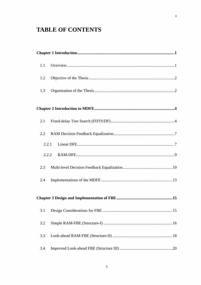
TABLE OF CONTENTS
Chapter 1 Introduction................................................................................................1
1.1 Overview..........................................................................................................1
1.2 Objective of the Thesis ....................................................................................2
1.3 Organization of the Thesis ...............................................................................2
Chapter 2 Introduction to MDFE...............................................................................4
2.1 Fixed-delay Tree Search (FDTS/DF)...............................................................4
2.2 RAM Decision Feedback Equalization............................................................7
2.2.1 Linear DFE................................................................................................7
2.2.2 RAM-DFE.................................................................................................9
2.3 Multi-level Decision Feedback Equalization.................................................10
2.4 Implementations of the MDFE ......................................................................13
Chapter 3 Design and Implementation of FBE.......................................................15
3.1 Design Considerations for FBE .....................................................................15
3.2 Simple RAM-FBE (Structure-I) ....................................................................16
3.3 Look-ahead RAM-FBE (Structure-II) ...........................................................18
3.4 Improved Look-ahead FBE (Structure III) ....................................................20
ii
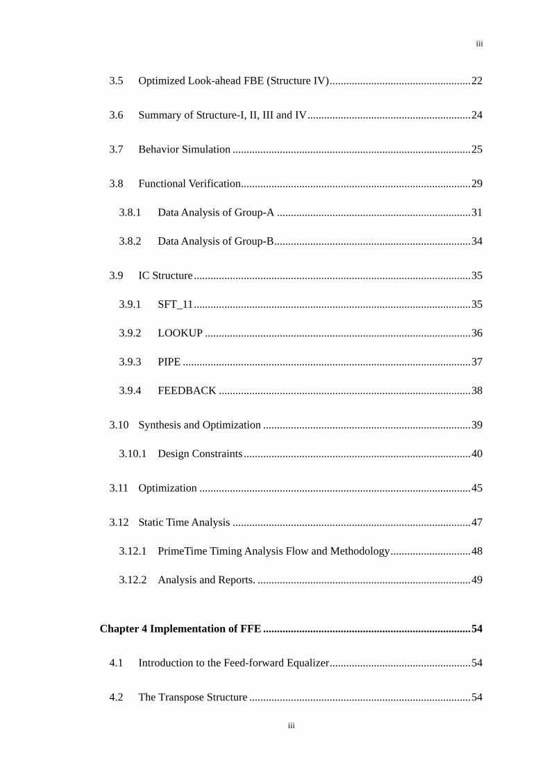
iii
3.5 Optimized Look-ahead FBE (Structure IV)...................................................22
3.6 Summary of Structure-I, II, III and IV...........................................................24
3.7 Behavior Simulation ......................................................................................25
3.8 Functional Verification...................................................................................29
3.8.1 Data Analysis of Group-A ......................................................................31
3.8.2 Data Analysis of Group-B.......................................................................34
3.9 IC Structure ....................................................................................................35
3.9.1 SFT_11....................................................................................................35
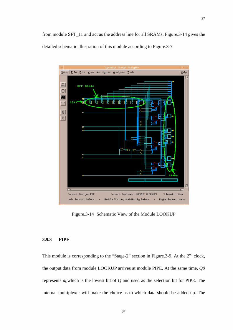
3.9.2 LOOKUP ................................................................................................36
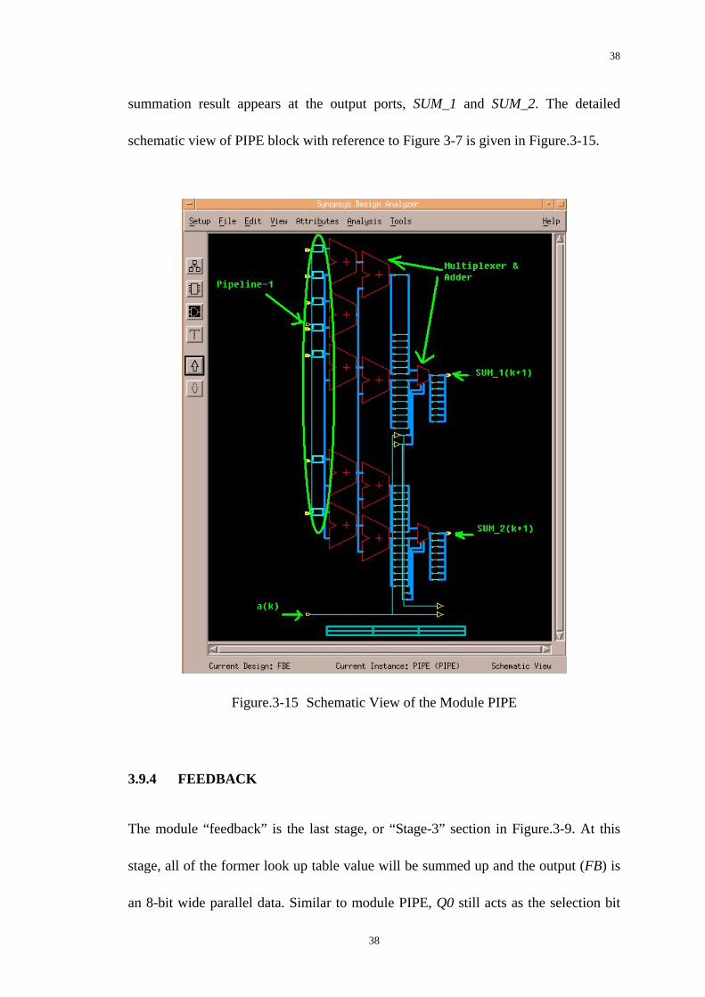
3.9.3 PIPE ........................................................................................................37
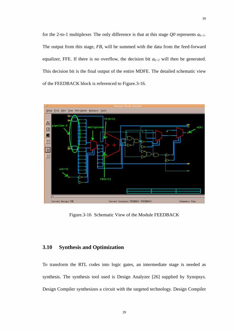
3.9.4 FEEDBACK ...........................................................................................38
3.10 Synthesis and Optimization ...........................................................................39
3.10.1 Design Constraints ..................................................................................40
3.11 Optimization ..................................................................................................45
3.12 Static Time Analysis ......................................................................................47
3.12.1 PrimeTime Timing Analysis Flow and Methodology.............................48
3.12.2 Analysis and Reports. .............................................................................49
Chapter 4 Implementation of FFE ...........................................................................54
4.1 Introduction to the Feed-forward Equalizer...................................................54
4.2 The Transpose Structure ................................................................................54
iii
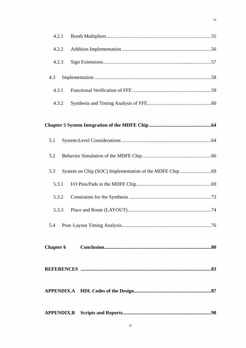
iv
4.2.1 Booth Multipliers ....................................................................................55
4.2.2 Addition Implementation ........................................................................56
4.2.3 Sign Extensions.......................................................................................57
4.3 Implementation ..............................................................................................58
4.3.1 Functional Verification of FFE ...............................................................59
4.3.2 Synthesis and Timing Analysis of FFE...................................................60
Chapter 5 System Integration of the MDFE Chip..................................................64
5.1 System-Level Considerations ........................................................................64
5.2 Behavior Simulation of the MDFE Chip .......................................................66
5.3 System on Chip (SOC) Implementation of the MDFE Chip .........................69
5.3.1 I/O Pins/Pads in the MDFE Chip............................................................69
5.3.2 Constraints for the Synthesis ..................................................................73
5.3.3 Place and Route (LAYOUT)...................................................................74
5.4 Post–Layout Timing Analysis........................................................................76
Chapter 6 Conclusion......................................................................................80
REFERENCES .........................................................................................................83
APPENDIX.A HDL Codes of the Design..............................................................87
APPENDIX.B Scripts and Reports.......................................................................98
iv
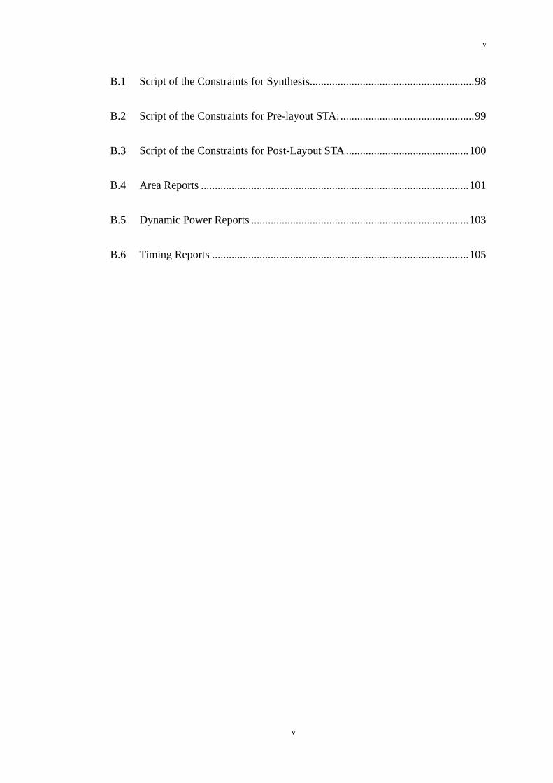
v
B.1 Script of the Constraints for Synthesis...........................................................98
B.2 Script of the Constraints for Pre-layout STA:................................................99
B.3 Script of the Constraints for Post-Layout STA ............................................100
B.4 Area Reports ................................................................................................101
B.5 Dynamic Power Reports ..............................................................................103
B.6 Timing Reports ............................................................................................105
v
vi
SUMMARY
The design and implementation of a Multi-level Decision Feedback Equalization
(MDFE) chip for magnetic recording channel is described. The architecture of the
single-chip MDFE incorporates an 8-tap feed-forward equalizer and a 10-tap feedback
equalizer. The feed-forward section (FFE) is a linear transposed filter that removes
the linear precursor inter-symbol interference (ISI) by a sufficient length to delay the
channel response to make it causal. The feedback section (FBE) uses the decision
feedback technique to eliminate non-linear postcursor ISI by a look-up table based
structure with the past decisions being the addresses, provided that the past decisions
are correct. The main idea of MDFE is to eliminate all the ISI and shape the recoding
channel with only impulse response plus some noise components remain.
The design is targeted at a 0.35µm CMOS technology. The minimum clock rate of the
chip is projected to be 150MHz with minimal sacrifice in the core area and the
dynamic power consumption. The final design shows that at post-layout level, the
MDFE chip can operate at a clock rate of 170MHz in TYPICAL condition, 230MHz in
BEST case, and 125MHz in WORST case. The speed can be further improved by
removing the bottleneck at the FFE, which only runs up to 185 MHz as opposed to
200 MHz for the FBE. The chip, which is composed of 73,386 gates and 54 I/O pads,
has the chip area of 4.4mm2, and consumes dynamic power of 143.03mW under a
3.3-V supply.
vi
vii
LIST OF TABLES
Table.2-1 Comparison of MDFE architectures....................................................14
Table.3-1 Data path delay of Structure-I .............................................................18
Table.3-2 Data path delay of Structure-II ............................................................20
Table.3-3 Core Area and Speed of Structure-III & II ..........................................21
Table.3-4 Comparison between Structure-IV & III .............................................23
Table.3-5 Comparison between Structure-IV & III .............................................23
Table.3-6 Summary of Structure-I, II, III & IV...................................................24
Table.3-7 Performance summary of FBE (Structure-IV) ....................................53
Table.4-1 Signal Description of FFE...................................................................59
Table.4-2 Performance of FFE ............................................................................63
Table.5-1 Signal Description of the MDFE chip.................................................65
Table.5-2 Data analysis for the MDFE chip ........................................................68
Table.5-3 I/O Ports and Pads Description of the MDFE chip. ............................72
Table.5-4 Performance of the MDFE chip at post-layout level...........................79
Table.6-1 Published DFE/MDFE filters/detectors...............................................81
vii
viii
LIST OF FIGURES
Figure.2-1 Fixed-delay tree search (FDTS/DF) detector.....................................4
Figure.2-2 FDTS/DF search algorithm................................................................5
Figure.2-3 Principle of FDTS/DF detection ........................................................6
Figure.2-4 Block diagram of the linear DFE.......................................................7
Figure.2-5 Block diagram of RAM-DFE.............................................................9
Figure.2-6 Digital communication channel with MDFE...................................11
Figure.3-1 System diagram of FFE and FBE ....................................................15
Figure.3-2 Block diagram of FBE (Structure-I) ................................................17
Figure.3-3 Segmentation of complicated combination logic.............................18
Figure.3-4 Block diagram of FBE (Structure-II) ...............................................19
Figure.3-5 Block diagram of FBE (Structure III) ..............................................21
Figure.3-7 Block diagram of FBE (Structure IV)..............................................22
Figure.3-8 Operation diagram of FBE...............................................................26
Figure.3-9 Clock waveform of FBE (Structure-IV) ..........................................28
Figure.3-10 FBE functional simulation data (for Group-A) ..............................30
Figure.3-11 FBE functional simulation data (for Group-B)...............................33
Figure.3-12 Schematic view of FBE ..................................................................35
Figure.3-13 I/O description of module SFT_11.................................................36
Figure.3-14 Schematic view of the module LOOKUP ......................................37
Figure.3-15 Schematic view of the module PIPE ..............................................38
viii
ix
Figure.3-16 Schematic view of the module FEEDBACK .................................39
Figure.3-17 Logic synthesis flow chart ..............................................................40
Figure.3-18 Waveform of input delay................................................................43
Figure.3-19 Waveform of output delay..............................................................44
Figure.3-20 User flow of PrimeTime .................................................................48
Figure.3-21 Histogramof path timing analysis...................................................52
Figure.4-1 FIR filter architecture used for FFE.................................................55
Figure.4-2 Block diagram of the feed-forward equalizer (FFE)........................58
Figure.4-3 Functional simulation for FFE.........................................................60
Figure.4-4 Leaf diagram of critical path in FFE................................................62
Figure.5-1 Block diagram of the MDFE chip....................................................65
Figure.5-2 Functional verification of the MDFE chip.......................................67
Figure.5-3 Schematic view of the combined system (full ports).......................70
Figure.5-4 Schematic view of the combined system (partial ports) ..................71
Figure.5-5 Diagram of the I/O pads of the chip.................................................73
Figure.5-6 Flow chart of the layout process ......................................................74
Figure.5-7 Layout view of the MDFE chip .......................................................75
Figure.5-8 Time waveform of the critical path (Pre-Layout level) ...................77
Figure.5-9 Time waveform of the critical path (Post-Layout level)..................77
ix
1
Chapter 1 Introduction
1.1 Overview
As the magnetic recording industry strives toward high recording densities, the design
of equalizers becomes one of the most crucial issues. Inter symbol interference (ISI) is
severe at high recording densities and causes degradation in the detection
performance because of the difficulty to achieve accurate equalization or because of
the excessive noise enhancement. Conventional read-back processing involves the use
of run-length limited (RLL) [1][2] codes with peak detection and some read-back
equalization. At recording densities in the range of 2-2.5, this turns out to be highly
inadequate. Several more sophisticated detection schemes which give improved
detection performance at high recording densities are now being pursued.
These schemes can be broadly classified into two categories: one is based on the
principle of partial-response signaling coupled with the maximum-likelihood
sequence detection (PRML) and the other is based on the principle of decision
feedback equalization (DFE). Class-IV PRML [3][4], and extended PRML [5][6] are
examples of the first category. Fixed-delay tree search with decision feedback
(FDTS/DF) [7], adaptive RAM-DFE [8][14] and multilevel DFE (MDFE) [9] are
examples of the second category.
1
2
The main idea of decision feedback is to cancel all the precursor and postcursor ISI of
the channel impulse response using a 2-tap filter. The feed-forward section (FFE) is a
linear filter that removes the linear precursor ISI by averaging and distributing the
energy to the postcursor ISI. The feedback equalizer (FBE) is a technique used to
eliminate non-linear postcursor ISI by the decision-feedback, provided that the past
decisions are correct, so that the output only consists of the impulse response plus
some noise components.
1.2 Objective of the Thesis
The objective of this thesis is to design and implement an integrated multilevel
decision feedback equalization chip for magnetic recoding channel. The MDFE chip
consists of a feed-forward and a feedback equalizer. The two sections could either run
together as a whole system or be tested independently. This design aims to attain a
minimum clock rate of 150MHz (typical-case) using 0.35µm CMOS technology with
minimal sacrifice in the core area and the dynamic power consumption.
1.3 Organization of the Thesis
The thesis is organized as follows. Chapter 2 introduces some background knowledge
about FDTS/DF, RAM-DFE and MDFE. Chapter 3 deals with the design and
implementation of the feedback equalizer (FBE). Several different architectures are
2
3
first investigated and compared, from which the final architecture of FBE is decided.
The functional simulation and static time analysis results are presented. Chapter 4
mainly concerns the implementation of the feed-forward equalizer (FFE). Chapter 5
presents the integration of FBE and FFE. The overall design is verified and further
synthesized to physical level. The post-layout analysis is carried out and the result is
presented. Finally, Chapter 6 concludes this research. Some future work is also
suggested.
3
4
Chapter 2 Introduction to MDFE
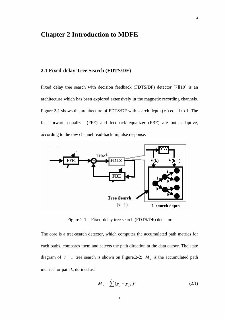
2.1 Fixed-delay Tree Search (FDTS/DF)
Fixed delay tree search with decision feedback (FDTS/DF) detector [7][10] is an
architecture which has been explored extensively in the magnetic recording channels.
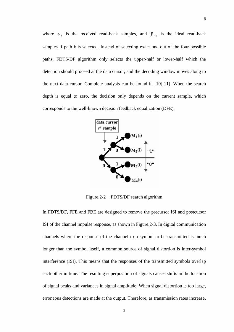
Figure.2-1 shows the architecture of FDTS/DF with search depth (τ ) equal to 1. The
feed-forward equalizer (FFE) and feedback equalizer (FBE) are both adaptive,
according to the raw channel read-back impulse response.
Figure.2-1 Fixed-delay tree search (FDTS/DF) detector
The core is a tree-search detector, which computes the accumulated path metrics for
each paths, compares them and selects the path direction at the data cursor. The state
diagram of 1=τ tree search is shown on Figure.2-2: is the accumulated path
metrics for path k, defined as:
kM
∑ −=τ
2)( ,kjjk yyM (2.1)
4
5
where is the received read-back samples, and jy kjy , is the ideal read-back
samples if path k is selected. Instead of selecting exact one out of the four possible
paths, FDTS/DF algorithm only selects the upper-half or lower-half which the
detection should proceed at the data cursor, and the decoding window moves along to
the next data cursor. Complete analysis can be found in [10][11]. When the search
depth is equal to zero, the decision only depends on the current sample, which
corresponds to the well-known decision feedback equalization (DFE).
Figure.2-2 FDTS/DF search algorithm
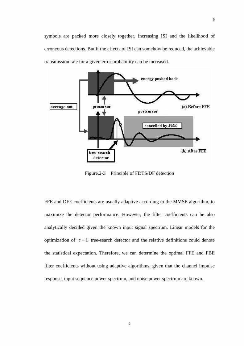
In FDTS/DF, FFE and FBE are designed to remove the precursor ISI and postcursor
ISI of the channel impulse response, as shown in Figure.2-3. In digital communication
channels where the response of the channel to a symbol to be transmitted is much
longer than the symbol itself, a common source of signal distortion is inter-symbol
interference (ISI). This means that the responses of the transmitted symbols overlap
each other in time. The resulting superposition of signals causes shifts in the location
of signal peaks and variances in signal amplitude. When signal distortion is too large,
erroneous detections are made at the output. Therefore, as transmission rates increase,
5
6
symbols are packed more closely together, increasing ISI and the likelihood of
erroneous detections. But if the effects of ISI can somehow be reduced, the achievable
transmission rate for a given error probability can be increased.
Figure.2-3 Principle of FDTS/DF detection
FFE and DFE coefficients are usually adaptive according to the MMSE algorithm, to
maximize the detector performance. However, the filter coefficients can be also
analytically decided given the known input signal spectrum. Linear models for the
optimization of 1=τ tree-search detector and the relative definitions could denote
the statistical expectation. Therefore, we can determine the optimal FFE and FBE
filter coefficients without using adaptive algorithms, given that the channel impulse
response, input sequence power spectrum, and noise power spectrum are known.
6
7
2.2 RAM Decision Feedback Equalization
Decision Feedback Equalization (DFE) [12] is another technique used to eliminate all
ISI so that the output consists only of the impulse response, plus some noise
component. The magnetic recording channel at high density exhibits significant
non-linear inter-symbol interference, which degrades the performance of linear
equalization techniques. The RAM-DFE is proposed as a solution to this problem, in
which a digital random access memory (RAM) is used in the feedback path of a
feedback equalizer (FBE). It is capable of canceling the non-linear post-cursor
inter-symbol interference (ISI).
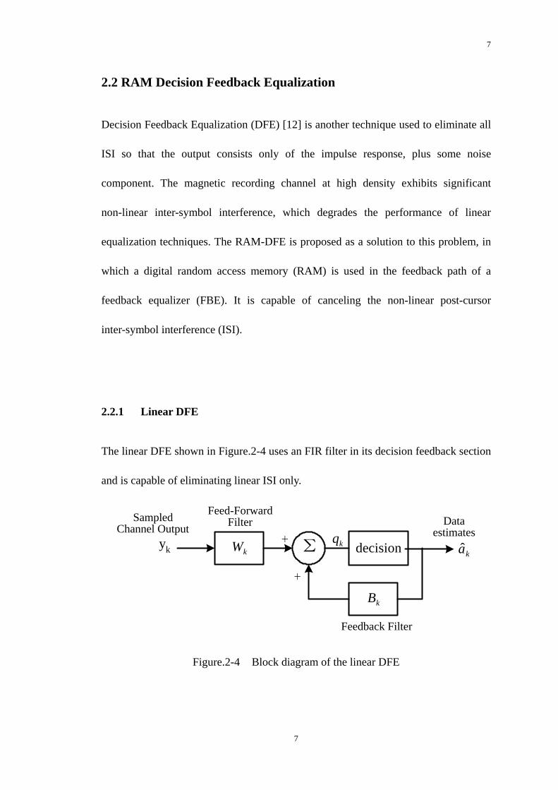
2.2.1 Linear DFE
The linear DFE shown in Figure.2-4 uses an FIR filter in its decision feedback section
and is capable of eliminating linear ISI only.
decisionΣ kqkW
kB
kayk+
+
Feed-ForwardFilter
Feedback Filter
SampledChannel Output
Dataestimates
Figure.2-4 Block diagram of the linear DFE
7
8
The linear DFE is described by (with L feed-forward coefficients and M feedback
coefficients is described by:
∑ ∑−
−+ +=1
1 ˆL M
mkmklk abywq= =0 1l m (2.2)
= MkkkLk abyw −−−+ + :1:1 ˆ'' (2.3)
with as the vector of channel outputs, and w and b as the
corresponding coefficient vectors of the linear DFE, and
. For notational convenience, we assume the feed-forward section to be
noncausal (realized with L units of delay). A good setting for the coefficient vectors in
the linear DFE minimizes the mean square error , where
]...[ 1:1 ′= −+−+ kLkkLk yyy
],...[ 10 ′= −Lwww
],...[ 1 ′= Mbbb
][ 2kE ε
kkk qa −=ε (2.4)
The corresponding settings for the linear DFE are well known to be computed as
, where 1][ −′=′′ Rpbw }]{[ :1:1 kMkkkLk aayEp −−−+ ′′=′ is the cross-correlation vector
between the current estimated data symbol and the vector of combined channel
outputs and previous decisions; and
ka
]}][{[ ayayER ′′′′= :1:1:1:1 MkkkLkMkkkLk −−−+−−−+
kmmse
(2.5)
is the autocorrelation matrix of the combined channel outputs and precious decisions.
Assuming correct output decisions, the minimum mean-square error (MMSE) is
pRpaE 122 }{ −′−=σ (2.6)
8
9
2.2.2 RAM-DFE
The RAM-DFE is shown in Figure.2-5, with linear feedback replaced by a lookup
table. We define the RAM-DFE parameters using a new notation. If M past decision
bits are arranged in a vector and used as a lookup table address, then we can interpret
the content of the addressed location as the corresponding table output.
decisionΣ kqkW
1~−kr
kayk+
+
Feed-ForwardFilter
Feedback Filter
SampledChannel Output
Dataestimates
Lookup Table
Figure.2-5 Block diagram of RAM-DFE
Let us denote an index for the address vector as 1~−ki , where can write
122)1(1~0 1
1
1 −≤+=≤ −−
−
− ∑ Mmmk
M
k ai20=m (2.7)
If we further define a 2M-dimensional vector
])~()...~(1)~([)~( ′= isisisis 1121101 −−−−− kkkk M (2.8)
then we can write the RAM output as
)~(~)~( ′= isbir 11 −− kk (2.9)
9
10
where ]~...~[~120 ′=−Mbbb is a vector with the contents of the corresponding ram
locations. Since the feedback path is linear in the 2M newly defined inputs, the
analysis is then the same as the linear DFE with replaced by , and b
replaced by
Mkka −− :1ˆ )~( 1−kis
b~ . The MMSE for the RAM-DFE is quadratic in the parameters
and has a unique global MMSE, because the autocorrelation matrix is nonsingular.
The 2
]~[ bw ′′
M elements of b~ are then the contents of the lookup table.
The MMSE for both the linear DFE and the RAM-DFE can be computed and
compared. The quantities p~ and R~ are not trivially computed in terms of the given
finite-state machine model for the channel. We show how to compute these quantities
in term of . The DFE output SNR in either case is computed as )( kif
2
22 )( mmsekaESNR
σσ−
=mmse (2.10)
In summary, RAM-DFE can very closely achieve the MMSE solution for the
measured read signal. Furthermore, by using signed-LMS, all explicit multiplications
may be eliminated from the adaptation procedure, making the RAM-DFE well suited
to high-speed applications such as magnetic recording.
2.3 Multi-level Decision Feedback Equalization
A simplified version of FDTS/DF [13] is called Multi-Level Decision Feedback
Equalization (MDFE) [9][15] because it is architecturally identical to DFE. The only
10
11
difference is that the algorithm for determining the coefficients of the forward and
backward equalizers is changed so that the output becomes multi-level. A digital
communication channel incorporating MDFE is shown in Figure2-6.
ChannelResponse Σ Σ
kqkrks
kW
kB
knkayk
+++
-
slicerForwardequalizer
Feedback equalizer
channel noise
b1+D
MDFE
Figure.2-6 Digital Communication Channel with MDFE
In this channel, a digital data stream, , consisting of positive and negative
impulses, enters the channel response block. The channel response block includes the
response of the transmission media, plus that of filters that are used to shape the signal
before and after its transmission. White noise is then factored in with the addition of
the term. After sampling, the transformed signal, , enters the MDFE through a
linear transversal filter - the forward FIR filter with coefficients . This filter is of
sufficient length to delay the response to make it causal. It is designed to remove
pre-cursor ISI from the response - the ISI due to future symbols.
ky
kn ks
kW
The output of the forward filter, , is summed with the output of the feedback
section. The coefficients of the feedback section, or backward filter, are chosen
kr
kB
11
12
to match the combined response of the channel block and the forward filter to a unit
impulse. In other words, when the output of the backward filter is subtracted from ,
all of the channel responses except for the unit impulse response of a single input
are removed.
kr
ky
The coefficients in MDFE are determined in the same way as in DFE. One difference
is the error signal, ( kkk qq ˆ−=ε ), due to the changed target, , and actual, ,
outputs in MDFE. Also, the b
kq kq
1 term is removed from its normal position in the
backward filter and is now calculated by a separate algorithm for its use in the linear
discriminant. Its equation is:
kkkkkbkk abaabb εµ )ˆ2ˆˆ(2 ,1111,11,1 ++−= −++ (2.11)
where 1bµ is the rate of adaptation for . kb ,1
Because the error signal, kε , now uses a future detected symbol, , a delay must
be added to the coefficient update equations for the forward and backward equalizers.
The update equation for the forward equalizer coefficients, ,
becomes:
1ˆ +ka
],...,,[ ,,1,0 kMkkk wwwW =
111 2 −−+ += kkwkk SWW εµ (2.12)
12
13
The update equation for the backward equalizer coefficients, ,
becomes:
],...,[ ,,21
kNkk bbB =
1111
1ˆ2 −−+ += kkbkk ABB εµ (2.13)
Once the values for b1, , and are calculated, and must be
multiplied through by the linear discriminant, (b
kW 1kB kW 1
kB
1 + D), to obtain the actual
coefficients to be loaded into the equalizers. Thus, the target response of MDFE is
multiplied by (b1 + D), yielding:
112
111 ˆˆ)1(ˆˆ −+ +++= kkkk abababq (2.14)
MDFE provides superior performance to the other disk data detection methods, such
as peak detection and Partial Response (PR) Equalization, while offering a simple,
low-cost, low-power implementation. Thus, MDFE is a promise solution for the
increasing disk drive storage density.
2.4 Implementations of the MDFE
The most significant differences between analog and digital implementation are the
non-idealities such as offset and nonlinearity that are associated with analog circuits.
Table.2-1 briefly compares the three architectures. If offset proves to be a
surmountable problem, the mostly analog MDFE will be the smallest of the three
implementations. It is reasonable to assume, with the design of the counters in the
13
14
mostly digital MDFE, the comparators will be the speed-limiting factor for all three
implementations. In this case the most efficient in terms of size and power will be the
mostly analog MDFE. For a completely digital implementation, the transposed FFE
and the RAM-DFE are worthy of consideration.
Table.2-1 Comparison of MDFE architectures
Architecture Programming Coefficients
Estimated Area Design Challenge
Analog Hard, ADC-DAC Smallest Integrator DC gain,offset Digital Easy Medium Fast digital circuits
Mixed-Signal Easy Largest Fast digital circuits, DAC
14
15
Chapter 3 Design and Implementation of FBE
3.1 Design Considerations for FBE
The block diagram of MDFE to be implemented is given in Figure 3-1. As described
before, the feed-forward section (FFE) is a linear filter that shapes the read-channel
pulse response, and the feedback section (FBE) is used to eliminate the non-linear
post-cursor ISI, provided that the past decisions are correct. An impulse response plus
some noise components will therefore be obtained at the output.
Σ kqkskW
kB
ka+
-
slicerForward equalizer
Feedback equalizer
Critical Loop
Channel Output Decision bit
Figure.3-1 System Diagram of FFE and FBE
being the addresses. A key specification for the FBE is the speed. When the current
decision is available, the feedback coefficient must be ready before next clock arrives.
Thus, the operation of the FBE must be completed within one clock cycle. This
imposed some difficulties on the FBE design. In this chapter, a number of
15
16
architectures for FBE are investigated and compared, from which the final
architecture is chosen. The number of taps and coefficients are determined from the
system-level simulation done elsewhere. The full digital implementation is a
prerequisite for this work. This design aims to attain a minimum clock rate of 150
MHz with minimal sacrifice in the core area and the dynamic power consumption.
3.2 Simple RAM-FBE (Structure-I)
A simple structure of the RAM-FBE, as shown in Figure.3-2, is first investigated It is
composed of a 12-tap D-Flip-Flop chain together with two SRAMs as the two look-up
tables. Each SRAM has the size of 26 ×8 bits. To achieve the goal of performing a
broad range of recording densities, minimizing the noise enhancement and a good
post-cursor ISI cancellation, the length of FBE must be long enough. The choice of
12-tap FBE is based on the work done in [17] where it showed that the satisfactory
performance can be achieved the minimum number of feedback taps of 12.
All the feedback coefficients are pre-calculated and loaded into the look-up tables
(LUT) through a series interface prior to the read operation of the channel. At the
rising clock edge of time k, for example, the past decisions stored in the D-Flip-Flop
chain are used to address the look-up tables. Two outputs from the lookup tables,
data_A and data_B are summed to produce the final feedback value FBk. This
feedback data is then added to the 8-bit output data, FEk, from the FFE. The slice
16
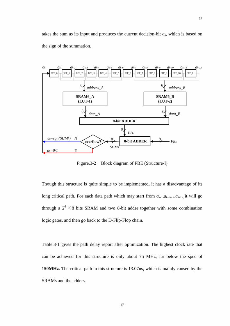
17
takes the sum as its input and produces the current decision-bit ak, which is based on
the sign of the summation.
DFF_0
SRAM6_B(LUT-2)
SRAM6_A(LUT-1)
8-bit ADDER
DFF_1 DFF_3 DFF_4 DFF_6DFF_5 DFF_7 DFF_8 DFF_9 DFF_10
FBk
FEk
data_A data_B
ak ak-1 ak-2 ak-4 ak-5 ak-6 ak-7 ak-8 ak-9 ak-10 ak-11
DFF_2
ak-3
DFF_11
ak-12
address_A address_B
overflow?ak=sgn(SUMk)
SUMkak=0/1
N
Y
6 6
8 8
8
88 8-bit ADDER
Figure.3-2 Block diagram of FBE (Structure-I)
Though this structure is quite simple to be implemented, it has a disadvantage of its
long critical path. For each data path which may start from ak-1,ak-2,…ak-12, it will go
through a 26 ×8 bits SRAM and two 8-bit adder together with some combination
logic gates, and then go back to the D-Flip-Flop chain.
Table.3-1 gives the path delay report after optimization. The highest clock rate that
can be achieved for this structure is only about 75 MHz, far below the spec of
150MHz. The critical path in this structure is 13.07ns, which is mainly caused by the
SRAMs and the adders.
17
18
Table.3-1 Data path delay of Structure-I
Path Through Path Delay ak-1 to data_A SRAM6_A 4.91 ns data_A to FBk 8-bit adder 3.78 ns FBk to SUMk 8-bit adder 3.82 ns SUMk to ak logic gates 0.56 ns
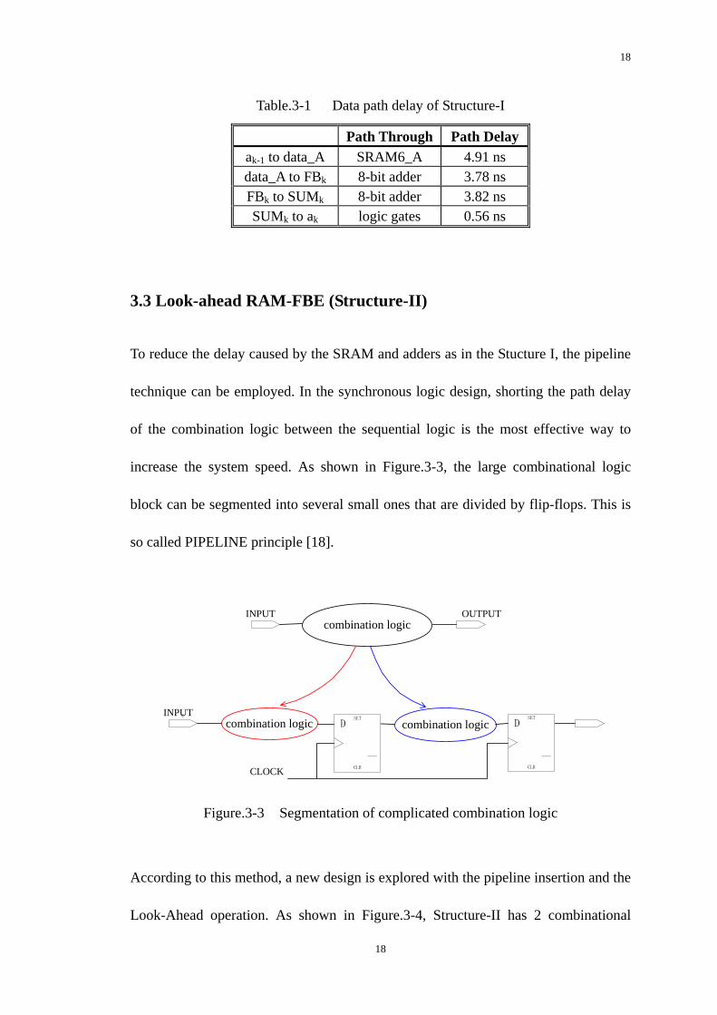
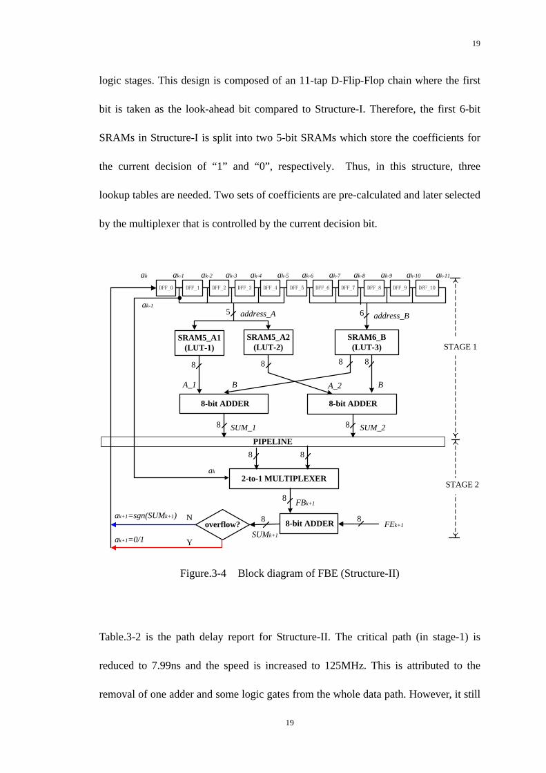
3.3 Look-ahead RAM-FBE (Structure-II)
To reduce the delay caused by the SRAM and adders as in the Stucture I, the pipeline
technique can be employed. In the synchronous logic design, shorting the path delay
of the combination logic between the sequential logic is the most effective way to
increase the system speed. As shown in Figure.3-3, the large combinational logic
block can be segmented into several small ones that are divided by flip-flops. This is
so called PIPELINE principle [18].
combination logicINPUT OUTPUT
c
combination logicINPUT
combination logic
CLOCK
SET
CLR
DSET
CLR
D
Figure.3-3 Segmentation of complicated combination logic
According to this method, a new design is explored with the pipeline insertion and the
Look-Ahead operation. As shown in Figure.3-4, Structure-II has 2 combinational
18
19
logic stages. This design is composed of an 11-tap D-Flip-Flop chain where the first
bit is taken as the look-ahead bit compared to Structure-I. Therefore, the first 6-bit
SRAMs in Structure-I is split into two 5-bit SRAMs which store the coefficients for
the current decision of “1” and “0”, respectively. Thus, in this structure, three
lookup tables are needed. Two sets of coefficients are pre-calculated and later selected
by the multiplexer that is controlled by the current decision bit.
DFF_0
SRAM6_B(LUT-3)
SRAM5_A1(LUT-1)
SRAM5_A2(LUT-2)
8-bit ADDER
PIPELINE
DFF_1 DFF_3 DFF_4 DFF_6DFF_5 DFF_7 DFF_8 DFF_9 DFF_10
2-to-1 MULTIPLEXER
SUM_1 SUM_2
FBk+1
FEk+1
ak
A_1 A_2 B
ak ak-1 ak-2 ak-4 ak-5 ak-6 ak-7 ak-8 ak-9 ak-10 ak-11
STAGE 1
STAGE 2
DFF_2
ak-3
ak-1
ak+1=sgn(SUMk+1)
SUMk+1ak+1=0/1
address_A address_B
8-bit ADDER
overflow?N
Y
8
88
B
8 8
8 8 8 8
8 8
5 6
8-bit ADDER
Figure.3-4 Block diagram of FBE (Structure-II)
Table.3-2 is the path delay report for Structure-II. The critical path (in stage-1) is
reduced to 7.99ns and the speed is increased to 125MHz. This is attributed to the
removal of one adder and some logic gates from the whole data path. However, it still
19
20
could not reach 150MHz for the bottleneck is still concern with the delay by SRAM.
Table.3-2 Data path delay of Structure-II
Path Path Through Path DelayStage-1 ak-1 to SUM_1 SRAM5_A1 & 1 8-bit adder 7.99 ns Stage-2 FBk to ak 1 8-bit adder & logic gates 3.76 ns
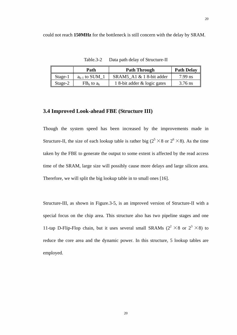
3.4 Improved Look-ahead FBE (Structure III)
Though the system speed has been increased by the improvements made in
Structure-II, the size of each lookup table is rather big (25 ×8 or 26 ×8). As the time
taken by the FBE to generate the output to some extent is affected by the read access
time of the SRAM, large size will possibly cause more delays and large silicon area.
Therefore, we will split the big lookup table in to small ones [16].
Structure-III, as shown in Figure.3-5, is an improved version of Structure-II with a
special focus on the chip area. This structure also has two pipeline stages and one
11-tap D-Flip-Flop chain, but it uses several small SRAMs (22 ×8 or 23 ×8) to
reduce the core area and the dynamic power. In this structure, 5 lookup tables are
employed.
20
21
DFF_0
SRAM3_C(LUT-4)
SRAM5_A1(LUT-1)
SRAM5_A2(LUT-2)
8-bit ADDER
PIPELINE
DFF_1 DFF_3 DFF_4 DFF_6DFF_5 DFF_7 DFF_8 DFF_9 DFF_10
2-to-1 MULTIPLEXER
SUM_1 SUM_2
FBk+1
FEk+1
ak
A_1 A_2 B
ak ak-1 ak-2 ak-4 ak-5 ak-6 ak-7 ak-8 ak-9 ak-10 ak-11
STAGE 1
STAGE 2
DFF_2
ak-3
ak-1
ak+1=sgn(SUMk+1)
SUMk+1ak+1=0/1
address_B
8-bit ADDER
overflow?N
Y
8
88
8 8
8 8 8
8 8
3
SRAM3_B(LUT-3)
SRAM3_D(LUT-5)
2 3 3address_A address_C address_D
88 C D
8-bit ADDER
Figure.3-5 Block diagram of FBE (Structure III)
Synthesis and simulation results show that there is a significant improvement on the
chip area in Structure II, while maintaining the same speed. The critical path is still in
Stage-1. Table.3-3 shows the performance comparison between Structure II and III.
The speed of the FBE needs to be further improved.
Table.3-3 Core Area and Speed of Structure-III & II
Critical Path Clock Rate Core Area Structure-II 7.99 ns 125 MHz 0.82 mm2
Structure-III 7.70 ns 130 MHz 0.26 mm2
21
22
3.5 Optimized Look-ahead FBE (Structure IV)
It has been found that the bottleneck for the speed in the previous structure is due to
the SRAM and the adder in Stage-1. Thus, the SRAMs can be further split to small
sizes and more pipelines can be employed. This leads to the Structure IV as shown
in Figure.3-7.
DFF_0
SRAM3_C(LUT-6)
SRAM3_D(LUT-7)
SRAM2_B(LUT-5)
SRAM2_A2(LUT-2)
SRAM2_A3(LUT-3)
SRAM2_A4(LUT-4)
SRAM2_A1(LUT-1)
PIPELINE_1
4-to-2 MULTIPLEXER
PIPELINE_2
DFF_1 DFF_2 DFF_3 DFF_5DFF_4 DFF_6 DFF_7 DFF_8 DFF_9
2-to-1 MULTIPLEXER
SUM_1k+1 SUM_2k+1
FBk+2
FEk+2
ak+2=sgn(SUMk+2)
ak
A_1 A_2 A_3 A_4 B C D
ak ak-1 ak-2 ak-3 ak-4 ak-5 ak-6 ak-7 ak-8 ak-9 ak-10
ak+1
ak-1
STAGE 1
STAGE 2
STAGE 3
SUMk+2ak+2=0/1
address_A address_B address_C address_D2 2 3 3
8888888
8888888
8-bit ADDER
8 8 8
8-bit ADDER 8-bit ADDER
8 8
8 8
overflow?N
Y
8
88 8-bit ADDER
A_1/A_3 A_2/A_4 B+C+D
Figure.3-7 Block diagram of FBE (Structure IV)
Structure IV has three pipeline stages and one 10-tap D-Flip-Flop chain. It looks
ahead for 2 bits, instead of just one as in the two previous structures. The first two
2-bit SRAM, which is in structure-III, are split into four 2-bit SRAMs which store the
coefficients for the current decision of “1” and “0” and the next decision of “1” and
22
23
“0” respectively. Thus, in this structure, seven lookup tables are needed. Four sets of
coefficients are pre-calculated and later selected by the multiplexer that is controlled
by the current decision bit and the next decision in different pipeline stages.
The three pipeline stages relax the timing constraint, while the 2-bit look ahead avoids
the problem of latency introduced by the pipeline stages. In this structure, although
seven lookup tables are needed, the size of each lookup table or RAM, which is 22 ×8
or 23 ×8, is still quite small.
Table.3-4 shows the path delay report of Structure IV. As the 2 pipeline stages in
Structure-II and III are split into 3 stages, here the critical path is no longer in Stage-1
but in Stage-2 only caused by the adders. It can be seen that evaluation the critical
path is reduced to 4.60ns and the speed of 200MHz is attained.
Table.3-4 Comparison between Structure-IV & III
Path Path Through Path Delay Stage-1 ak-12 to D SRAM3_D 3.91 ns Stage-2 D to SUM_1 2 8-bit adders 4.60 ns Stage-3 FBk to ak 1 8-bit adder & logic gates 3.47 ns
Table.3-5 shows the comparison with the Structure III. The chip area is 0.33 mm2,
only slightly larger than that of Structure-III (0.26 mm2).
Table.3-5 Comparison between Structure-IV & III
Critical Path Speed Core Area Structure-III 7.70 ns 130 MHz 0.26 mm2 Structure-IV 4.60 ns 200 MHz 0.33 mm2
23
24
3.6 Summary of Structure-I, II, III and IV
The performances of the four structures are summarized in Table.3-6. Structure-I is a
direct implementation based on the operation of the MDFE. Although it is simple, it
has the worst performance. The speed improvement of both Structure-II and
Structure-III are benefited from the pipeline technique. Structure-III has the smallest
core area which is achieved by replacing the big SRAMs with small ones. However,
both of them are limited at the frequency of no more than 130MHz. Structure IV
shows superior speed performance to the other three structures with slightly larger
core area and high power consumption than those of Structure III. Its speed
performance is attributed to its 3 pipeline and the use of small SRAMs. The Structure
IV is finally chosen for the implementation of FBE.
Table.3-6 Summary of Structure-I, II, III & IV
Structure I II III IV
Taps
12 11 11 10
Pipeline Stages
No pipeline 2 2 3
SRAM 26×8 bits (×2) 25×8 bits (×2)26×8 bits (×1)
22×8 bits (×2) 23×8 bits (×3)
22×8 bits (×5)23×8 bits (×2)
Clock Rate (MHz)
75 125 130 200
Core Area (mm2)
/ 0.82 0.26 0.33
Dynamic Power (mW)
/ 1091.7 18.39 43.86
24
25
3.7 Behavior Simulation
Behavior simulation is quite necessary when the system-level design is done. There
are several ways to create an imaginary simulation model of a system. The behavioral
simulation gives out the verification that if a logical system works correctly. The
simulation tool used here is Verilog-XL.3.0 [24][25] by CADENCE. In the next
subsections, the verification result and the data analysis of FBE and the whole system
will be given.
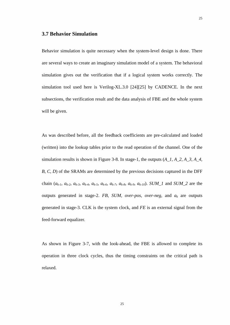
As was described before, all the feedback coefficients are pre-calculated and loaded
(written) into the lookup tables prior to the read operation of the channel. One of the
simulation results is shown in Figure 3-8. In stage-1, the outputs (A_1, A_2, A_3, A_4,
B, C, D) of the SRAMs are determined by the previous decisions captured in the DFF
chain (ak-1, ak-2, ak-3, ak-4, ak-5, ak-6, ak-7, ak-8, ak-9, ak-10). SUM_1 and SUM_2 are the
outputs generated in stage-2. FB, SUM, over-pos, over-neg, and ak are outputs
generated in stage-3. CLK is the system clock, and FE is an external signal from the
feed-forward equalizer.
As shown in Figure 3-7, with the look-ahead, the FBE is allowed to complete its
operation in three clock cycles, thus the timing constraints on the critical path is
relaxed.
25
26
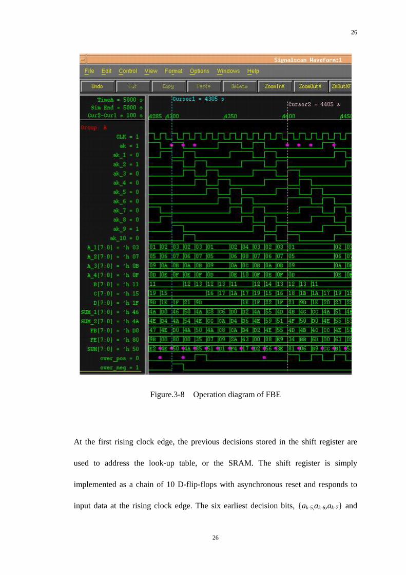
Figure.3-8 Operation diagram of FBE
At the first rising clock edge, the previous decisions stored in the shift register are
used to address the look-up table, or the SRAM. The shift register is simply
implemented as a chain of 10 D-flip-flops with asynchronous reset and responds to
input data at the rising clock edge. The six earliest decision bits, {ak-5,ak-6,ak-7} and
26
27
{ak-8,ak-9,ak-10} are used to address SRAM_C and SRAM_D, respectively. The two
second recent decision bits, {ak-3, ak-4}, are used to address SRAM_B and the two
most recent decision bits, {ak-1,ak-2}, address four look-up tables, SRAM2_A1(for the
case of ak=0, ak+1=0), SRAM2_A2(for the case of ak=0, ak+1=1), SRAM2_A3(for the
case of ak=1, ak+1=0), and SRAM2_A4(for the case of ak=1, ak+1=1).
At the second rising clock edge, 4 possible values of FB are summed up by the
previous 7 output data from the 7 look-up tables. At the same time, the current
decision bit ak is clocked into the first bit in the shift register, and this value is used as
the select signal for the 4 to 2 multiplexer to choose the corresponding SUM_1 and
SUM_2 from the 4 sum values. The computation of the 2nd stage outputs are shown in
the following 2 equations.
⎩⎨⎧
+++===
+++===
++
++
DCBAaaSUM
DCBAaaSUM
kkk
kkk
2_)1,0(|2_
1_)0,0(|1_
11
11 (3.1)
or,
⎩⎨⎧
+++===+++===
++
++
DCBAaaSUMDCBAaaSUM
kkk
kkk
4_)1,1(|2_3_)0,1(|1_
11
11 (3.2)
At the third rising clock edge, the current decision bit ak+1 is clocked into the first bit
in the shift register. This value is used as the select signal for the 2 to 1 multiplexer to
choose the corresponding FBk+2 from the two pre-calculated feedback values like
following:
⎩⎨⎧
====
+++
+++
112
112
2_)1(|1_)0(|
kkk
kkk
SUMaFBSUMaFB
(3.3)
27
28
The final feedback value FBk+2 will then be summed with the 8-bit input from the
feed-forward filter. FEk+2 at the main adder to produce ak+2, which is based on the sign
of the summation. The computation of the 3rd stage outputs are:
222 +++ += kkk FBFESUM (3.4)
In the case of no overflow:
) (3.5) sgn( 22 ++ = kk SUMa
In the case of positive or negative overflow:
⎩⎨⎧
−=−=
+
+
)(;1)(;0
2
2
overflowposaoverflowposa
k
k (3.6)
.
Figure.3-9 Clock waveform of FBE (Structure-IV)
The above operation is illustrated in Figure.3-9, in which it shows that the operation
of the FBE is completed in three clock cycles.
28
29
3.8 Functional Verification
To do the functional verification, hundreds of vectors are fed into FBE as the
simulated input data FE (8-bit). Therefore, the outputs of FBE could be verified, such
as FB, SUM, and ak. Figure.3-10 and Figure.3-11 shows the behavioral simulation
result of FBE by vectors. Each data line presents for the variables in FBE system and
they are listed by time. From the data, we could have an analysis that if this system is
running just as correctly as predicted.
As the system is a feedback loop and the only factors which could influence the whole
operation are ak and FE, especially ak, the analysis could be taken out by Typical
Cases. Totally such kinds of cases are 6 and they could be classified by 2 groups.
Group-A includes 4 cases which mainly concern with the operation with different
ak/ak+1, for ak is to verify the logic in stage-2 and ak+1 is to verify the logic in Stage-3.
Group-B includes the other 2 cases which concern with the data overflow. For these
two cases, ak/ak+1 are not relevant.
Typical Case.1: ak = 0, ak+1 = 0;
Typical Case.2: ak = 1, ak+1 = 0;
Typical Case.3: ak = 0, ak+1 = 1;
Typical Case.4: ak = 1, ak+1 = 1;
Typical Case.5: positive overflow;
Typical Case.6: negative overflow;
Figure.3-10 and Figure.3-11 have exactly the same simulation data, and the only difference is they have different markers to show the case analysis of Group-A and Group-B respectively.
29
30
Figure.3-10 FBE functional simulation data (for Group-A)
30
31
3.8.1 Data Analysis of Group-A
Typical Case.1: ak = 0, ak+1 = 0;
At time k = 4160,
A_1=4, A_2=8, A_3=12, A_4= 16, B= 19, C=28, D=157
At time k+1 = 4170, ak=0, according to (3.1),
SUM_1k+1 | (ak=0, ak+1=0) = 4+19+28+157 = 208SUM_2k+1 | (ak=0, ak+1=1) = 8+19+28+157 = 212
At time k+2 = 4180, ak+1=0, according to (3.3),
FBk+2|( ak+1=0) = SUM_1k+1=208
In the meanwhile, FE k+2 = 0, according to (3.4),
SUMk+2= 208+0 =208
There is no data overflow, so according to (3.5),
ak+2 = sgn (SUMk+2) = 1
Typical Case.2 ak = 1, ak+1 = 0;
At time k = 4220,
A_1=1, A_2=5, A_3=9, A_4= 13, B= 19, C=25, D=34
At time k+1 = 4230, ak=1, according to (3.2),
SUM_1k+1 | (ak=1, ak+1=0) = 9+19+25+34 = 87SUM_2k+1 | (ak=1, ak+1=1) = 13+19+25+34 = 91
At time k+2 = 4240, ak+1=0, according to (3.3),
FBk+2|( ak+1=0) = SUM_1k+1= 87
In the meanwhile, FE k+2 = 203, according to (3.4),
SUMk+2= 203+87 = 34
There is no data overflow, so according to (3.5),
ak+2 = sgn (SUMk+2) = 0
31
32
Typical Case.3 ak = 0, ak+1 = 1;
At time k = 4300,
A_1=2, A_2=6, A_3=10, A_4=14, B= 17, C=21, D=30
At time k+1 = 4310, ak=0, according to (3.1),
SUM_1k+1 | (ak=0, ak+1=0) = 2+17+21+30 = 70SUM_2k+1 | (ak=0, ak+1=1) = 6+17+21+30 = 74
At time k+2 = 4320, ak+1=1, according to (3.3),
FBk+2|( ak+1=1) = SUM_2k+1= 74
In the meanwhile, FE k+2 = 0, according to (3.4),
SUMk+2= 0+74 = 74
There is no data overflow, so according to (3.5),
ak+2 = sgn (SUMk+2) = 0
Typical Case.4 ak = 1, ak+1 = 1;
At time k = 4350,
A_1=1, A_2=5, A_3=9, A_4= 13, B= 19, C=23, D=157
At time k+1 = 4360, ak=1, according to (3.2),
SUM_1k+1 | (ak=1, ak+1=0) = 9+19+23+157 = 208SUM_2k+1 | (ak=1, ak+1=1) = 13+19+23+157 = 212
At time k+2 = 4370, ak+1=1, according to (3.3),
FBk+2|( ak+1=1) = SUM_2k+1= 212
In the meanwhile, FE k+2 = 67, according to (3.4),
SUMk+2= 67+212 = 23
There is no data overflow, so according to (3.5),
ak+2 = sgn (SUMk+2) = 0
32
33
Figure.3-11 FBE functional simulation data (for Group-B)
33
34
3.8.2 Data Analysis of Group-B
Typical Case.5 Positive Overflow;
At time k = 4250, A_1=1, A_2=5, A_3=9, A_4= 13, B= 18, C=25, D=33
At time k+1 = 4260, ak=0, according to (3.1),
SUM_1k+1 | (ak=0, ak+1=0) = 1+18+25+33 = 77SUM_2k+1 | (ak=0, ak+1=1) = 5+18+25+33 = 81
At time k+2 = 4270, ak+1=0, according to (3.3),
FBk+2|( ak+1=0) = SUM_1k+1= 77
In the meanwhile, FE k+2 = 52, according to (3.4),
SUMk+2= 52+77 = 129
There is a positive overflow (pos=1), so according to (3.6),
ak+1 = 0;
Typical Case.6 Negative Overflow;
At time k = 4290, A_1=1, A_2=5, A_3=9, A_4= 13, B= 17, C=25, D=157
At time k+1 = 4300, ak=1, according to (3.2),
SUM_1k+1 | (ak=1, ak+1=0) = 9+17+25+157 = 208SUM_2k+1 | (ak=1, ak+1=1) = 13+17+25+157 = 212
At time k+2 = 4310, ak+1=0, according to (3.3),
FBk+2|( ak+1=0) = SUM_1k+1= 208
In the meanwhile, FE k+2 = 128, according to (3.4),
SUMk+2= 128+208 = 80
There is a negative overflow (neg=1), so according to (3.6),
ak+1 = 1;
34
35
From the analysis with the 6 typical cases, we could get conclusion that it is a good
functional simulation with correct logic verification.
3.9 IC Structure
The schematic view of the synthesized FBE is shown in Figure.3-12. The entire FBE
structure is composed by 4 functional sub-modules, namely, SFT_11, LOCKUP, PIPE
and FEEDBACK.
Figure.3-12 Schematic View of FBE
3.9.1 SFT_11
This module is a “Series-to-Parallel Converter” which is required for SRAM’s
initialization. In the earlier description, the largest SRAM in the FBE is 23×8, which
means that its address width is 3 bits and the data width is 8 bits. Therefore, an 11-bit
35
36
parallel data is needed to initialize the SRAM with the pre-determined lookup table
values. In other words, 11 I/O pads are needed for this purpose. To reduce the number
of pads, a series data input is chosen.
Figure.3-13 shows the port declaration of this module. “Ini” is the series input port
and “Initial_Data” is the 11-bits parallel output port. There are 11 D-flip-flops in it to
achieve the function as a “Series-to-Parallel Converter”.
Figure.3-13 I/O description of module SFT_11
3.9.2 LOOKUP
This module contains 7 SRAM’s and 10 D-flip-flops which is just corresponding to
the “Stage-1” section in Figure.3-9. Input ak is the current decision bit generated by
the critical loop itself, and the output Q is a 10-bit wide parallel data which present for
the latest 10 decision bits latched in the D-flip-flop chains. In other words, it is Q that
addresses SRAM2_A_1, SRAM2_A_2, SRAM2_A_3, SRAM2_A_4, SRAM2_B,
SRAM3_C and SRAM3_D at the same time. Therefore, the outputs A_1, A_2, A_3,
A_4, B, C, and D are the output data from those SRAMs at the current clock. The
other input ports WE_A_1, WE_A_2, WE_A_3, WE_A_4, WE_B, WE_C, WE_D, and
Initial_Data are used for SRAM initialization, and the port “Initial_Data” comes
36
37
from module SFT_11 and act as the address line for all SRAMs. Figure.3-14 gives the
detailed schematic illustration of this module according to Figure.3-7.
Figure.3-14 Schematic View of the Module LOOKUP
3.9.3 PIPE
This module is corresponding to the “Stage-2” section in Figure.3-9. At the 2nd clock,
the output data from module LOOKUP arrives at module PIPE. At the same time, Q0
represents ak which is the lowest bit of Q and used as the selection bit for PIPE. The
internal multiplexer will make the choice as to which data should be added up. The
37
38
summation result appears at the output ports, SUM_1 and SUM_2. The detailed
schematic view of PIPE block with reference to Figure 3-7 is given in Figure.3-15.
Figure.3-15 Schematic View of the Module PIPE
3.9.4 FEEDBACK
The module “feedback” is the last stage, or “Stage-3” section in Figure.3-9. At this
stage, all of the former look up table value will be summed up and the output (FB) is
an 8-bit wide parallel data. Similar to module PIPE, Q0 still acts as the selection bit
38
39
for the 2-to-1 multiplexer. The only difference is that at this stage Q0 represents ak+1.
The output from this stage, FB, will be summed with the data from the feed-forward
equalizer, FFE. If there is no overflow, the decision bit ak+2 will then be generated.
This decision bit is the final output of the entire MDFE. The detailed schematic view
of the FEEDBACK block is referenced to Figure.3-16.
Figure.3-16 Schematic View of the Module FEEDBACK
3.10 Synthesis and Optimization
To transform the RTL codes into logic gates, an intermediate stage is needed as
synthesis. The synthesis tool used is Design Analyzer [26] supplied by Synopsys.
Design Compiler synthesizes a circuit with the targeted technology. Design Compiler
39
40
also optimizes logic designs for speed, area, and other factors. This optimization is
performed for hierarchical combinational or sequential circuit design descriptions.
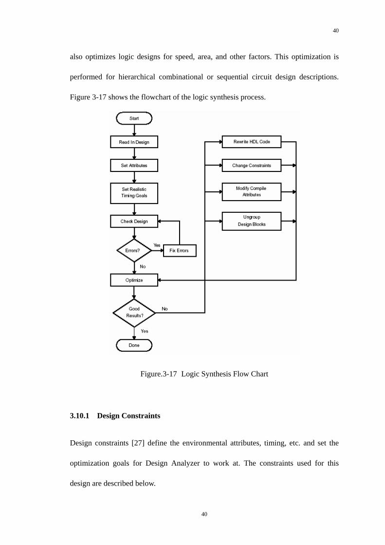
Figure 3-17 shows the flowchart of the logic synthesis process.
Figure.3-17 Logic Synthesis Flow Chart
3.10.1 Design Constraints
Design constraints [27] define the environmental attributes, timing, etc. and set the
optimization goals for Design Analyzer to work at. The constraints used for this
design are described below.
40
41
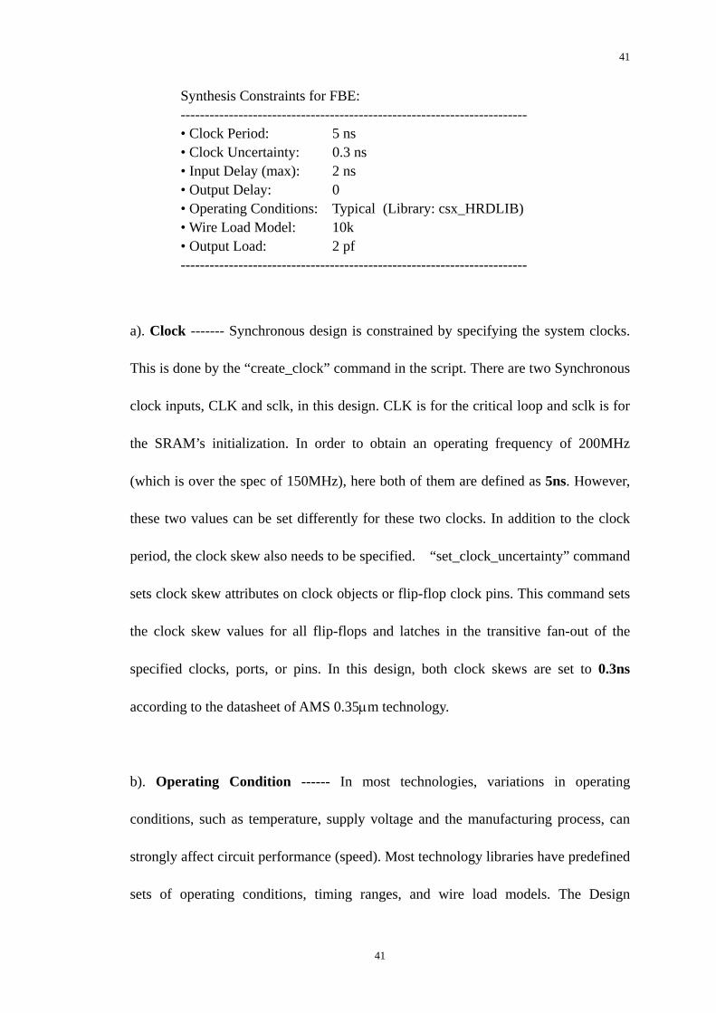
Synthesis Constraints for FBE: ------------------------------------------------------------------------ • Clock Period: 5 ns • Clock Uncertainty: 0.3 ns • Input Delay (max): 2 ns • Output Delay: 0 • Operating Conditions: Typical (Library: csx_HRDLIB) • Wire Load Model: 10k • Output Load: 2 pf ------------------------------------------------------------------------
a). Clock ------- Synchronous design is constrained by specifying the system clocks.
This is done by the “create_clock” command in the script. There are two Synchronous
clock inputs, CLK and sclk, in this design. CLK is for the critical loop and sclk is for
the SRAM’s initialization. In order to obtain an operating frequency of 200MHz
(which is over the spec of 150MHz), here both of them are defined as 5ns. However,
these two values can be set differently for these two clocks. In addition to the clock
period, the clock skew also needs to be specified. “set_clock_uncertainty” command
sets clock skew attributes on clock objects or flip-flop clock pins. This command sets
the clock skew values for all flip-flops and latches in the transitive fan-out of the
specified clocks, ports, or pins. In this design, both clock skews are set to 0.3ns
according to the datasheet of AMS 0.35µm technology.
b). Operating Condition ------ In most technologies, variations in operating
conditions, such as temperature, supply voltage and the manufacturing process, can
strongly affect circuit performance (speed). Most technology libraries have predefined
sets of operating conditions, timing ranges, and wire load models. The Design
41

42
Compiler timing analyzer uses this library information when performing a static delay
analysis. To ensure that acceptable performance levels are maintained over a range of
operating conditions, optimization is carried out within the specified operation
conditions.
In this design, the operating condition is set as “TYPICAL” case, which means that
the supply voltage is 3.3V, the process (scaling factor to account for variations in the
semiconductor manufacturing process) is as default as 1.00, the temperature is 25.00
OC, and the interconnect model (tree_type for driving pins and network loads) is also
as default as the balanced case. Apart from the typical case, the simulations are also
done for different corners, such as WORST case and BEST case, and the report could
be found in Table.3-5 at the end of this chapter.
c). Wire Load Mode ------ Design Compiler uses wire load models to estimate the
resistance, capacitance, and area of nets before floor planning or layout. The wire load
models, provided by the technology library, define a fanout-to-length relationship, and
the “fanout” is the total number of pins on the net excluding the driver pin. If Design
Compiler encounters a fanout count greater than the largest fanout_length pair, it uses
the slope value to extrapolate the wire length. In AMS’s technology library
csx_HRDLIB.db, 10k, 30k and 100k are three types of wire load model,
Normally Design Compiler will automatically pick the correct wire load model based
on area. According to this design (core area = 0.33 mm2) which was mentioned before,
42
43
model 10k is then be chosen as the max wire load model.
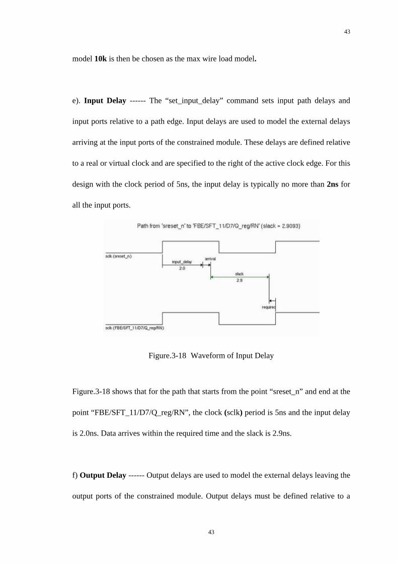
e). Input Delay ------ The “set_input_delay” command sets input path delays and
input ports relative to a path edge. Input delays are used to model the external delays
arriving at the input ports of the constrained module. These delays are defined relative
to a real or virtual clock and are specified to the right of the active clock edge. For this
design with the clock period of 5ns, the input delay is typically no more than 2ns for
all the input ports.
Figure.3-18 Waveform of Input Delay
Figure.3-18 shows that for the path that starts from the point “sreset_n” and end at the
point “FBE/SFT_11/D7/Q_reg/RN”, the clock (sclk) period is 5ns and the input delay
is 2.0ns. Data arrives within the required time and the slack is 2.9ns.
f) Output Delay ------ Output delays are used to model the external delays leaving the
output ports of the constrained module. Output delays must be defined relative to a
43
44
real or virtual clock to be considered a path constraint. Output delays are defined to
the left of the active clock edge; this delay corresponds to the time before the next
rising edge. In this design, the output ports are not driving any other subsequent
blocks but are mainly for test purpose, so it is unnecessary to set output delay
value.(The default value is zero)
Figure.3-19 Waveform of Output Delay
In order to make it clear, Figure.3-19 shows an example of the output delay waveform.
The clock period is 20ns, and the output delay is 4ns, so the absolute time should be
no more than 16ns.
g) Output Load ------ The “set_load” command places a load on a port or a net. The
units of this load must be consistent with the technology library. This value is used for
timing optimizations, not for maximum fanout optimizations. Since during the test,
the output ports drive the test instrument. With reference to our existing test
instrument (Logic Analyzer) whose input capacitance is 2pF, the output load value
here is set to 2pF.
44

45
3.11 Optimization
Optimization (compiling) [28] is the step in the synthesis process that attempts to
implement a combination of library cells that meets the functional, speed, and area
requirements of the design. Optimization transforms a design into a
technology-specific circuit based on the attributes and constraints placed on the
design.
There are several ways to achieve the same logic but use the different instances or
different structure. If the design is mainly concerned with the SPEED, more
complicated instances, such as parallel structures, could be used instead of simple
ones. If the design is mainly concerned with the CHIP AREA, simpler instances
should be taken though the speed may be degraded.
To account for the inaccuracy of the modeling and other unpredicted effects and
ensure that the specifications are met, the system is sometime over constrained.
Over constraint is to constrain the design more than it is required by the specifications.
The disadvantage of this method is that under the over constraint condition, the area
of the design may be larger than what it is required and more resources are used.
Thus a trade-off is needed.
Once all of the initial steps are completed the optimization can be executed. Different
options allow further control of this process. In hierarchically structured systems, the
45

46
option "boundary optimization" is of importance. Activating this option allows the
optimization to take place across module boundaries and permits the inversion of port
signals.
Another parameter controlling the relative amount of CPU time spent during the
mapping phase is the "map effort". By specifying ‘-map_effort low’, it takes the least
time to compile but could only run a test to check the logic. Low is not recommended
if the design must meet timing or area goals. On the other hand, using the option
‘-map_effort high’ can produce better designs. The mapping process proceeds until it
has tried all strategies. However, high forces the tool to exhaust all possible strategies
for the optimization, so it takes significantly longer time to compile. Normally,
“-map_effort medium” is used as the default setting because Design Compiler tries to
find a good mapping but does not use some CPU-intensive strategies. Medium is
appropriate for getting a quick idea of how large a circuit will be, and it is used for
most cases, also in this design.
When the optimization is done, the design will be synthesized to the gate level and
mapped into a gate-level netlist.
46
47
3.12 Static Time Analysis
Static timing analysis is an exhaustive method of analyzing, debugging, and validating
design performance. First, a design is analyzed and then all possible paths are timed
(without enumerating individual paths) and checked against the requirements. The
advantages of using this method are fast operation and identification of critical paths.
For some tools such as PrimeTime [29] the disadvantages of using this method are that
false paths are often identified as being in violation and static-timing analysis is
typically restricted to the synchronous portions of a design.
The EDA tool used for static time analysis in this project is Primetime, a stand-alone,
full-chip, gate-level static timing analyzer from synopsys. PrimeTime performs timing
analysis at the gate level and provides a comprehensive set of modeling technologies
for representing non-synthesized blocks for analysis. This technology includes three
elements which are stamp modeling language, model extraction, and quick timing
models. It provides functions to support both top-down and bottom-up design
methodologies. The PrimeTime is a static timing analyzer, which means that it does not
activate the circuit with many input vectors and measure the delay. Instead, it uses a
library which contains timing information about these standard cells, identifies all the
paths in the design, and finds out the critical path (maximum worst case delay from
input to output). In this sense, it is "static".
47
48
3.12.1 PrimeTime Timing Analysis Flow and Methodology
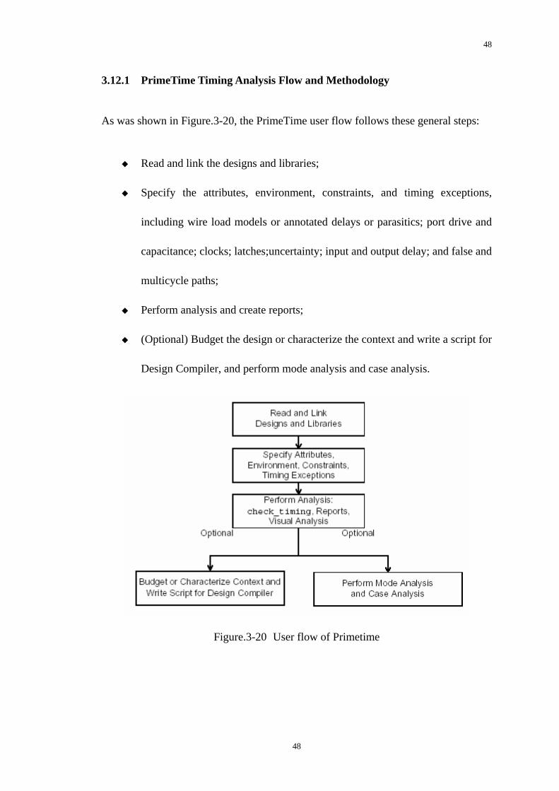
As was shown in Figure.3-20, the PrimeTime user flow follows these general steps:
Read and link the designs and libraries;
Specify the attributes, environment, constraints, and timing exceptions,
including wire load models or annotated delays or parasitics; port drive and
capacitance; clocks; latches;uncertainty; input and output delay; and false and
multicycle paths;
Perform analysis and create reports;
(Optional) Budget the design or characterize the context and write a script for
Design Compiler, and perform mode analysis and case analysis.
Figure.3-20 User flow of Primetime
48
49
3.12.2 Analysis and Reports.
Followed by the steps above, the static timing analysis was carried out. the results will
be discussed and analysized in this section.
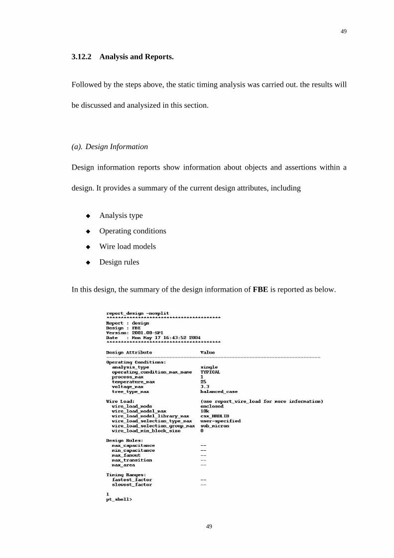
(a). Design Information
Design information reports show information about objects and assertions within a
design. It provides a summary of the current design attributes, including
Analysis type
Operating conditions
Wire load models
Design rules
In this design, the summary of the design information of FBE is reported as below.
49
50
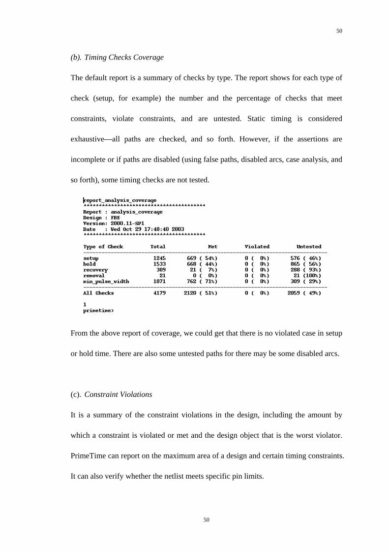
(b). Timing Checks Coverage
The default report is a summary of checks by type. The report shows for each type of
check (setup, for example) the number and the percentage of checks that meet
constraints, violate constraints, and are untested. Static timing is considered
exhaustive—all paths are checked, and so forth. However, if the assertions are
incomplete or if paths are disabled (using false paths, disabled arcs, case analysis, and
so forth), some timing checks are not tested.
From the above report of coverage, we could get that there is no violated case in setup
or hold time. There are also some untested paths for there may be some disabled arcs.
(c). Constraint Violations
It is a summary of the constraint violations in the design, including the amount by
which a constraint is violated or met and the design object that is the worst violator.
PrimeTime can report on the maximum area of a design and certain timing constraints.
It can also verify whether the netlist meets specific pin limits.
50
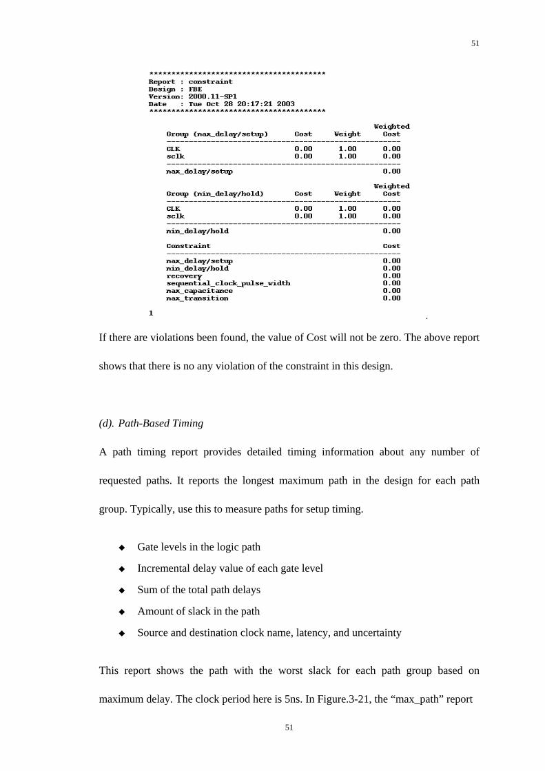
51
.
If there are violations been found, the value of Cost will not be zero. The above report
shows that there is no any violation of the constraint in this design.
(d). Path-Based Timing
A path timing report provides detailed timing information about any number of
requested paths. It reports the longest maximum path in the design for each path
group. Typically, use this to measure paths for setup timing.
Gate levels in the logic path
Incremental delay value of each gate level
Sum of the total path delays
Amount of slack in the path
Source and destination clock name, latency, and uncertainty
This report shows the path with the worst slack for each path group based on
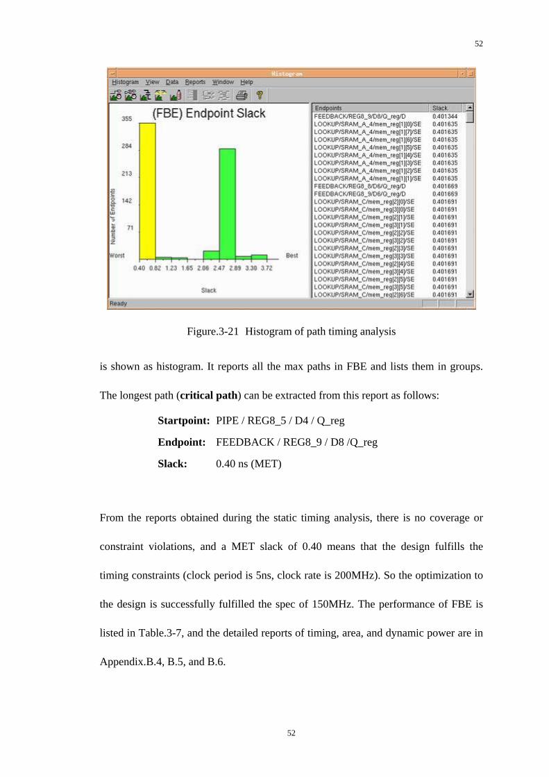
maximum delay. The clock period here is 5ns. In Figure.3-21, the “max_path” report
51
52
Figure.3-21 Histogram of path timing analysis
is shown as histogram. It reports all the max paths in FBE and lists them in groups.
The longest path (critical path) can be extracted from this report as follows:
Startpoint: PIPE / REG8_5 / D4 / Q_reg
Endpoint: FEEDBACK / REG8_9 / D8 /Q_reg
Slack: 0.40 ns (MET)
From the reports obtained during the static timing analysis, there is no coverage or
constraint violations, and a MET slack of 0.40 means that the design fulfills the
timing constraints (clock period is 5ns, clock rate is 200MHz). So the optimization to
the design is successfully fulfilled the spec of 150MHz. The performance of FBE is
listed in Table.3-7, and the detailed reports of timing, area, and dynamic power are in
Appendix.B.4, B.5, and B.6.
52
53
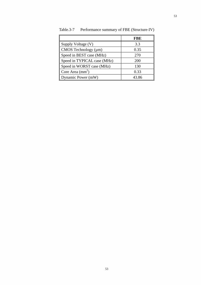
Table.3-7 Performance summary of FBE (Structure-IV)
FBE Supply Voltage (V) 3.3 CMOS Technology (µm) 0.35 Speed in BEST case (MHz) 270 Speed in TYPICAL case (MHz) 200 Speed in WORST case (MHz) 130 Core Area (mm2) 0.33 Dynamic Power (mW) 43.86
53
54
Chapter 4 Implementation of FFE
4.1 Introduction to the Feed-forward Equalizer
The feed-forward equalizer (FFE) is implemented as a fully digital 8-tap
programmable FIR filter. The FIR is realized using the transposed form architecture.
The multipliers are of parallel array type that uses radix-4 modified Booth encoding
[19] and a carry save partial product reduction scheme. The accumulation of filter
terms is performed in carry save format at each tap, with a pipelined carry propagate
adder merging the carry and sum vectors after the last stage. To account for
programmable coefficients, an 8×8-bit SRAM is implemented to store the 8-tap
coefficients. The speed of the filter is defined as the rate at which input samples can
be processed. To increase the speed, it is necessary to reduce the critical path delay
between input and output.
4.2 The Transpose Structure
Application of the transposition theorem [20] results in the transpose direct form
structure as shown in Fig.4.1 in which input is fed to all of the coefficient multipliers
in parallel and the results are accumulated over N sample periods, where N is the filter
order. This structure retains the regularity of the linear accumulation direct form
structure but has a delay equal to Tm + Ta, Tm is the multiplier delay and Ta is the
54
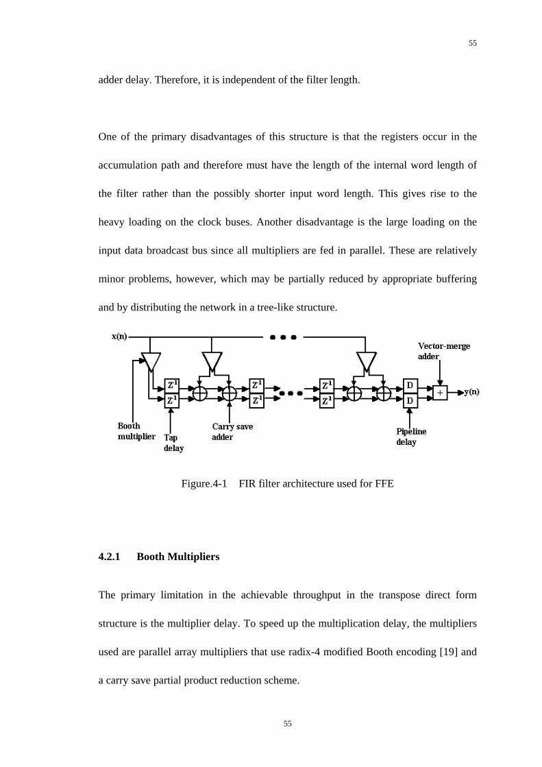
55
adder delay. Therefore, it is independent of the filter length.
One of the primary disadvantages of this structure is that the registers occur in the
accumulation path and therefore must have the length of the internal word length of
the filter rather than the possibly shorter input word length. This gives rise to the
heavy loading on the clock buses. Another disadvantage is the large loading on the
input data broadcast bus since all multipliers are fed in parallel. These are relatively
minor problems, however, which may be partially reduced by appropriate buffering
and by distributing the network in a tree-like structure.
Figure.4-1 FIR filter architecture used for FFE
4.2.1 Booth Multipliers
The primary limitation in the achievable throughput in the transpose direct form
structure is the multiplier delay. To speed up the multiplication delay, the multipliers
used are parallel array multipliers that use radix-4 modified Booth encoding [19] and
a carry save partial product reduction scheme.
55
56
The modified Booth algorithm is based on encoding the 2’s complement operand (i.e.
multiplier) in order to reduce the number of partial products to be added. This makes
the multiplier faster and uses less hardware (area). For example, the radix-4 modified
Booth algorithm is based on partitioning the multiplier into overlapping groups of 3-b,
and each group is decoded to generate the correct partial product. A detailed
explanation of the Booth algorithm can be found in [19]
4.2.2 Addition Implementation
The next limiting factor in the achievable throughput is due to the classic problem of
carry propagation. The simple carry ripple adder circuit is limited by its ripple path
delay which is proportional to the word length of the adder. To avoid the long critical
path of the carry ripple adder, the adders in each tap position are converted to carry
save adders.
A so-called vector-merge adder (VMA) [23] has to be used in the final stage to add
the final sum and carry as shown in Figure.4-1. The VMA is really just a carry
propagate adder. Since only one carry propagate adder is required, it is possible to use
one of the more complex fast adder techniques without an excessive impact on the
total area. A pipelined carry ripple adder is employed here for the VMA.
There are a few drawbacks to the carry save scheme, however, with the most
56
57
important of these being the negative impact of doubling the number of registers
required within the filter core. This increase in area is a price that must be paid in
order to achieve a high throughout which is the goal of this work.
4.2.3 Sign Extensions
With increasing parallelism, the amount of shifts between the partial products and
intermediate sums to be added tends to increase. When obeying the rules of 2’s
complement arithmetic the sign bits of the numbers to be added have to be extended
up to the most significant bit of the expected sum. This leads to a multiple and
redundant addition of the most significant bits in each row of adders which further on
leads to additional full adders per row. This slows down the circuit’s speed and
increases the layout area.
Hence, a modified 2’s complement number representation is derived [21], this scheme
is equal to a subsection of the algorithm already derived by Baogh-Wooley [22]. The
modified 2’s complement number representation together with algorithms for the
simplified addition of 2’s complement numbers [21] can eliminate the need of the
common sign bit extension in additions so that all adder cells of the multiplier have
the same load. This leads to an optimal transistor sizing and to an appropriate area
reduction.
57
58
4.3 Implementation
The FFE implements two blocks as shown in Figure.4-2:
Front-end
Back-end
The front consists of an 11-bit shift-left register to shift the data in serially and an 8 ×
8-bit register-based dual-port SRAM to store the 8-tap coefficients. The back consists
of the transposed-formed FIR filter described in the previous section. Table.4-1 is the
description of the signals presented in Figure.4-2.
sdata
pdata
pdata_ack
ShiftRegister
CoefficientRAM
CLK
FEFIR
Front-end Back-end
VMA
6
3
8
8
8
8
8
8
8
8
8
14
148
D1
addr
coeff
C0
C1
C2
C3
C4
C5
C6
C7
D2PipelineDelay
14 r
Figure.4-2 Block diagram of the Feed-forward Equalizer (FFE)
58
59
Table.4-1 Signal Description of FFE
Signal width I/O attribute Description CLK / Input System clock pdata_ack 1 bit Input Valid input data acknowledgement pdata 6 bits Input Input data for FFE sdata 1 bit Input Initialization data for the look-up-tables in
FFE addr 3 bits Inter-connection Address for the lookup table coeff 8 bits Inter-connection Coefficient for the lookup table C0 8 bits Inter-connection Coefficient for the 1st tap C1 8 bits Inter-connection Coefficient for the 2nd tap C2 8 bits Inter-connection Coefficient for the 3rd tap C3 8 bits Inter-connection Coefficient for the 4th tap C4 8 bits Inter-connection Coefficient for the 5th tap C5 8 bits Inter-connection Coefficient for the 6th tap C6 8 bits Inter-connection Coefficient for the 7th tap C7 8 bits Inter-connection Coefficient for the 8th tap D1 14 bits Inter-connection Data generated by the FIR D2 14 bits Inter-connection Data generated by the FIR r 14 bits Inter-connection Output from VMA FE 8 bits Output Equalized output from FFE
4.3.1 Functional Verification of FFE
Figure.4-3 gives out the functional simulation result of FFE. From the data presented,
we could get that there is totally 10 clock cycles to complete a full operation from
input to output.
Before time k = 4080, ack=0;
There is no valid input data
At time k = 4080, ack=1;
With the first valid input data pdata (6-bit); No valid coefficient out yet.
59
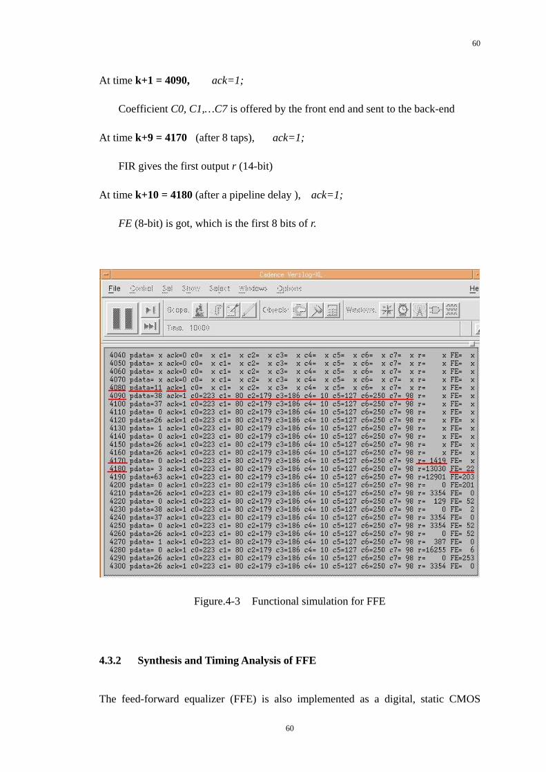
60
At time k+1 = 4090, ack=1;
Coefficient C0, C1,…C7 is offered by the front end and sent to the back-end
At time k+9 = 4170 (after 8 taps), ack=1;
FIR gives the first output r (14-bit)
At time k+10 = 4180 (after a pipeline delay ), ack=1;
FE (8-bit) is got, which is the first 8 bits of r.
Figure.4-3 Functional simulation for FFE
4.3.2 Synthesis and Timing Analysis of FFE
The feed-forward equalizer (FFE) is also implemented as a digital, static CMOS
60
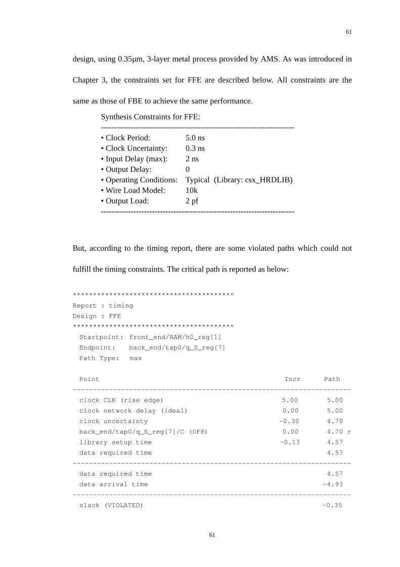
61
design, using 0.35µm, 3-layer metal process provided by AMS. As was introduced in
Chapter 3, the constraints set for FFE are described below. All constraints are the
same as those of FBE to achieve the same performance.
Synthesis Constraints for FFE: ------------------------------------------------------------------------ • Clock Period: 5.0 ns • Clock Uncertainty: 0.3 ns • Input Delay (max): 2 ns • Output Delay: 0 • Operating Conditions: Typical (Library: csx_HRDLIB) • Wire Load Model: 10k • Output Load: 2 pf ------------------------------------------------------------------------
But, according to the timing report, there are some violated paths which could not
fulfill the timing constraints. The critical path is reported as below:
****************************************
Report : timing
Design : FFE
****************************************
Startpoint: front_end/RAM/h0_reg[1]
Endpoint: back_end/tap0/q_S_reg[7]
Path Type: max
Point Incr Path
---------------------------------------------------------------------
clock CLK (rise edge) 5.00 5.00
clock network delay (ideal) 0.00 5.00
clock uncertainty -0.30 4.70
back_end/tap0/q_S_reg[7]/C (DF8) 0.00 4.70 r
library setup time -0.13 4.57
data required time 4.57
---------------------------------------------------------------------
data required time 4.57
data arrival time -4.93
---------------------------------------------------------------------
slack (VIOLATED) -0.35
61
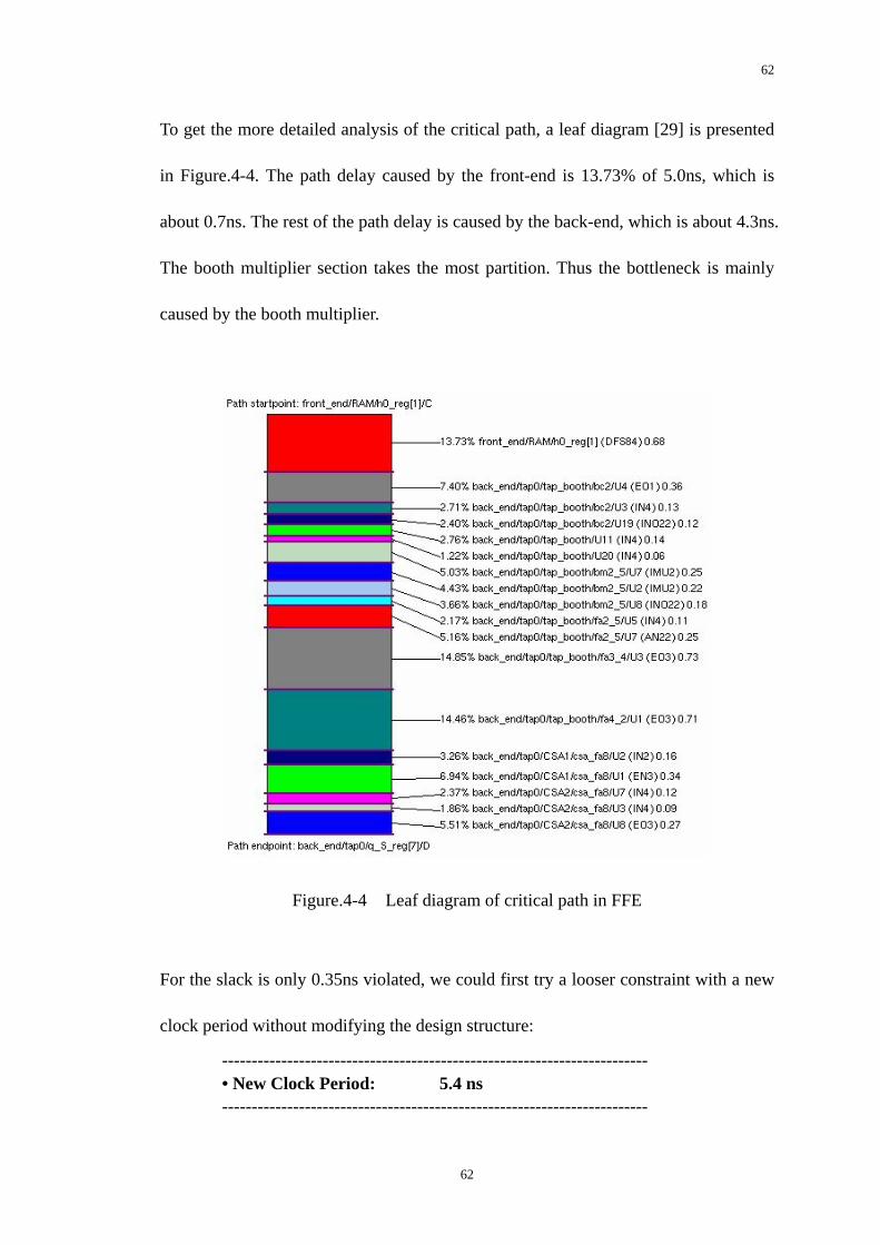
62
To get the more detailed analysis of the critical path, a leaf diagram [29] is presented
in Figure.4-4. The path delay caused by the front-end is 13.73% of 5.0ns, which is
about 0.7ns. The rest of the path delay is caused by the back-end, which is about 4.3ns.
The booth multiplier section takes the most partition. Thus the bottleneck is mainly
caused by the booth multiplier.
Figure.4-4 Leaf diagram of critical path in FFE
For the slack is only 0.35ns violated, we could first try a looser constraint with a new
clock period without modifying the design structure:
------------------------------------------------------------------------ • New Clock Period: 5.4 ns ------------------------------------------------------------------------
62
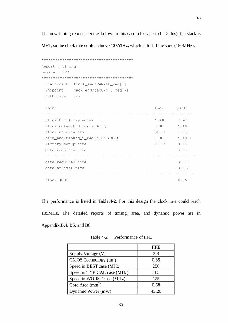
63
The new timing report is got as below. In this case (clock period = 5.4ns), the slack is
MET, so the clock rate could achieve 185MHz, which is fulfill the spec (150MHz).
****************************************
Report : timing
Design : FFE
****************************************
Startpoint: front_end/RAM/h0_reg[1]
Endpoint: back_end/tap0/q_S_reg[7]
Path Type: max
Point Incr Path
-------------------------------------------------------------------
clock CLK (rise edge) 5.40 5.40
clock network delay (ideal) 0.00 5.40
clock uncertainty -0.30 5.10
back_end/tap0/q_S_reg[7]/C (DF8) 0.00 5.10 r
library setup time -0.13 4.97
data required time 4.97
-------------------------------------------------------------------
data required time 4.97
data arrival time -4.93
-------------------------------------------------------------------
slack (MET) 0.05
The performance is listed in Table.4-2. For this design the clock rate could reach
185MHz. The detailed reports of timing, area, and dynamic power are in
Appendix.B.4, B5, and B6.
Table.4-2 Performance of FFE
FFE Supply Voltage (V) 3.3 CMOS Technology (µm) 0.35 Speed in BEST case (MHz) 250 Speed in TYPICAL case (MHz) 185 Speed in WORST case (MHz) 125 Core Area (mm2) 0.68 Dynamic Power (mW) 45.20
63
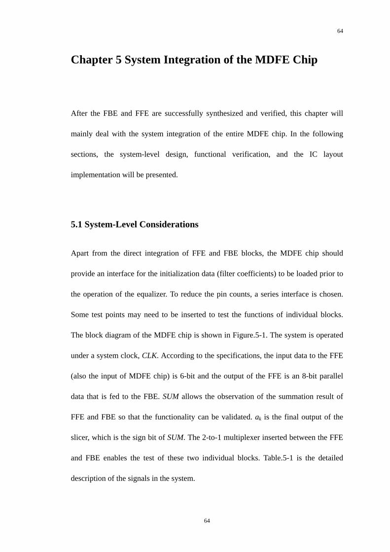
64
Chapter 5 System Integration of the MDFE Chip
After the FBE and FFE are successfully synthesized and verified, this chapter will
mainly deal with the system integration of the entire MDFE chip. In the following
sections, the system-level design, functional verification, and the IC layout
implementation will be presented.
5.1 System-Level Considerations
Apart from the direct integration of FFE and FBE blocks, the MDFE chip should
provide an interface for the initialization data (filter coefficients) to be loaded prior to
the operation of the equalizer. To reduce the pin counts, a series interface is chosen.
Some test points may need to be inserted to test the functions of individual blocks.
The block diagram of the MDFE chip is shown in Figure.5-1. The system is operated
under a system clock, CLK. According to the specifications, the input data to the FFE
(also the input of MDFE chip) is 6-bit and the output of the FFE is an 8-bit parallel
data that is fed to the FBE. SUM allows the observation of the summation result of
FFE and FBE so that the functionality can be validated. ak is the final output of the
slicer, which is the sign bit of SUM. The 2-to-1 multiplexer inserted between the FFE
and FBE enables the test of these two individual blocks. Table.5-1 is the detailed
description of the signals in the system.
64
65
ForwardEqualizer
FeedbackEqualizer
BEGIN
pdata
pdata_ack
CLK
FB
SUM
over_posover_neg
ak
Begin
2-to-1Multliplexer
TEST“1”
“0”
68
8
TEST_FE8
8 FE8
Figure.5-1 Block diagram of the MDFE chip
Table.5-1 Signal Description of the MDFE chip
Signal width I/O attribute Description CLK / Input System clock pdata_ack 1 bit Input Valid input data acknowledgement pdata 6 bits Input Input data for FFE sdata 1 bit Input Initialization data for the look-up-tables
in FFE Ini 1 bit Input Initialization data for the look-up-tables
in FBE Begin 1 bit Inter-connection Valid data detection for FBE FE 8 bits Inter-connection Output data from FFE / input data to
FBE FB 8 bits Output Output data from FBE SUM 8 bits Output Summation of FE and FB over_pos 1 bit Output Positive overflow detection over_neg 1 bit Output Negative overflow detection ak 1 bit Output Decision bit, output from the slicer
As described in Chapter 4, the output of the FFE will only be ready after 10 clock
cycles from the time when FFE starts receiving valid input data. Therefore, section
65
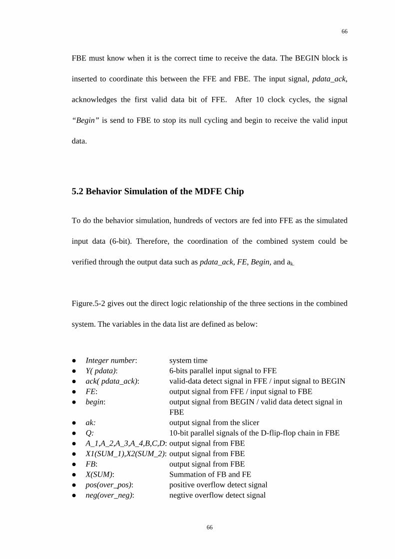
66
FBE must know when it is the correct time to receive the data. The BEGIN block is
inserted to coordinate this between the FFE and FBE. The input signal, pdata_ack,
acknowledges the first valid data bit of FFE. After 10 clock cycles, the signal
“Begin” is send to FBE to stop its null cycling and begin to receive the valid input
data.
5.2 Behavior Simulation of the MDFE Chip
To do the behavior simulation, hundreds of vectors are fed into FFE as the simulated
input data (6-bit). Therefore, the coordination of the combined system could be
verified through the output data such as pdata_ack, FE, Begin, and ak.
Figure.5-2 gives out the direct logic relationship of the three sections in the combined
system. The variables in the data list are defined as below:
Integer number: system time Y( pdata): 6-bits parallel input signal to FFE ack( pdata_ack): valid-data detect signal in FFE / input signal to BEGIN FE: output signal from FFE / input signal to FBE begin: output signal from BEGIN / valid data detect signal in
FBE ak: output signal from the slicer Q: 10-bit parallel signals of the D-flip-flop chain in FBE A_1,A_2,A_3,A_4,B,C,D: output signal from FBE X1(SUM_1),X2(SUM_2): output signal from FBE FB: output signal from FBE X(SUM): Summation of FB and FE pos(over_pos): positive overflow detect signal neg(over_neg): negtive overflow detect signal
66
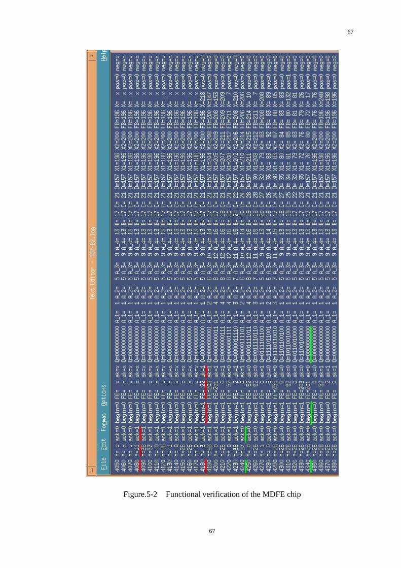
67
Figure.5-2 Functional verification of the MDFE chip
67
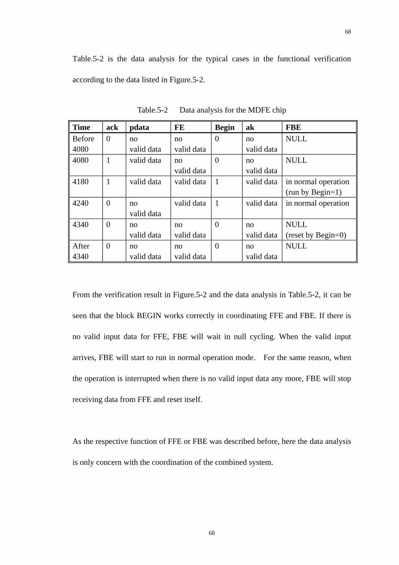
68
Table.5-2 is the data analysis for the typical cases in the functional verification
according to the data listed in Figure.5-2.
Table.5-2 Data analysis for the MDFE chip
Time ack pdata FE Begin ak FBE Before 4080
0 no valid data
no valid data
0 no valid data
NULL
4080 1 valid data no valid data
0 no valid data
NULL
4180 1 valid data valid data 1 valid data in normal operation (run by Begin=1)
4240 0 no valid data
valid data 1 valid data in normal operation
4340 0 no valid data
no valid data
0 no valid data
NULL (reset by Begin=0)
After 4340
0 no valid data
no valid data
0 no valid data
NULL
From the verification result in Figure.5-2 and the data analysis in Table.5-2, it can be
seen that the block BEGIN works correctly in coordinating FFE and FBE. If there is
no valid input data for FFE, FBE will wait in null cycling. When the valid input
arrives, FBE will start to run in normal operation mode. For the same reason, when
the operation is interrupted when there is no valid input data any more, FBE will stop
receiving data from FFE and reset itself.
As the respective function of FFE or FBE was described before, here the data analysis
is only concern with the coordination of the combined system.
68
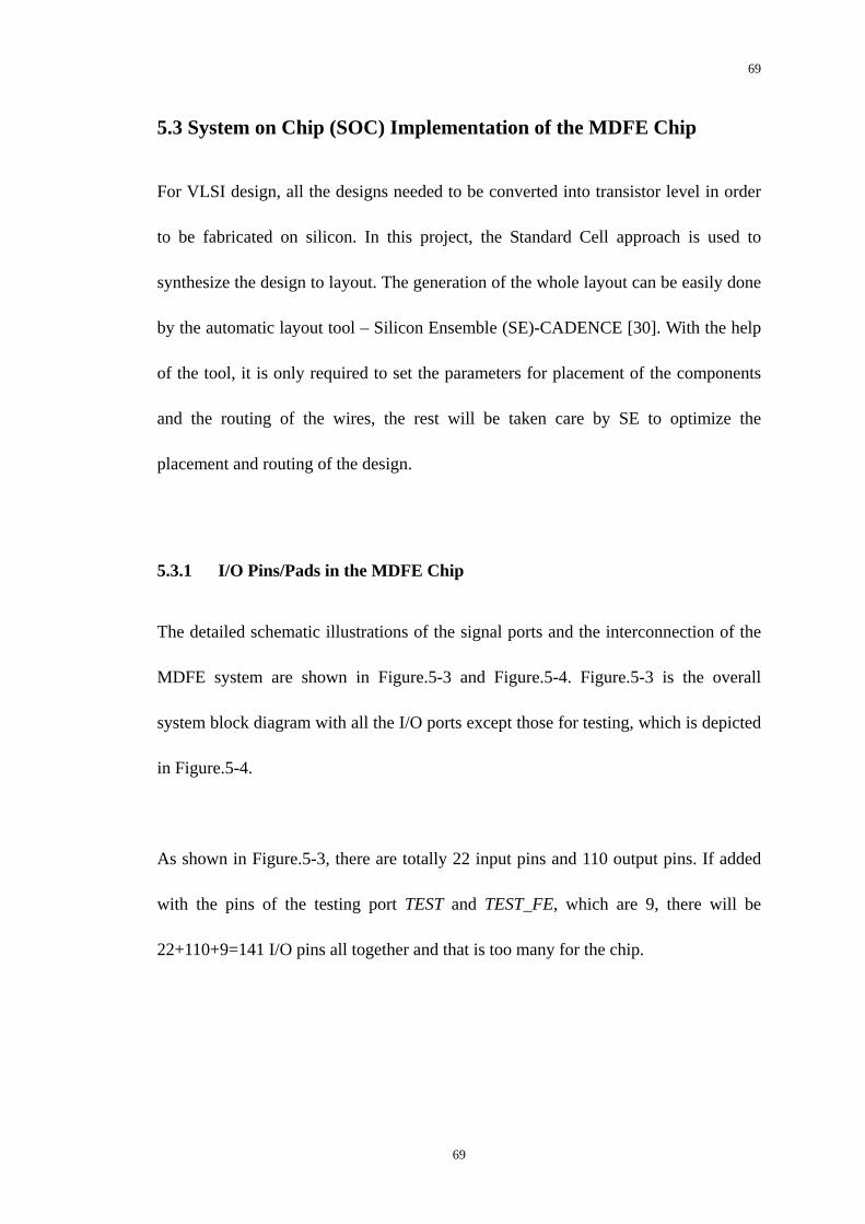
69
5.3 System on Chip (SOC) Implementation of the MDFE Chip
For VLSI design, all the designs needed to be converted into transistor level in order
to be fabricated on silicon. In this project, the Standard Cell approach is used to
synthesize the design to layout. The generation of the whole layout can be easily done
by the automatic layout tool – Silicon Ensemble (SE)-CADENCE [30]. With the help
of the tool, it is only required to set the parameters for placement of the components
and the routing of the wires, the rest will be taken care by SE to optimize the
placement and routing of the design.
5.3.1 I/O Pins/Pads in the MDFE Chip
The detailed schematic illustrations of the signal ports and the interconnection of the
MDFE system are shown in Figure.5-3 and Figure.5-4. Figure.5-3 is the overall
system block diagram with all the I/O ports except those for testing, which is depicted
in Figure.5-4.
As shown in Figure.5-3, there are totally 22 input pins and 110 output pins. If added
with the pins of the testing port TEST and TEST_FE, which are 9, there will be
22+110+9=141 I/O pins all together and that is too many for the chip.
69
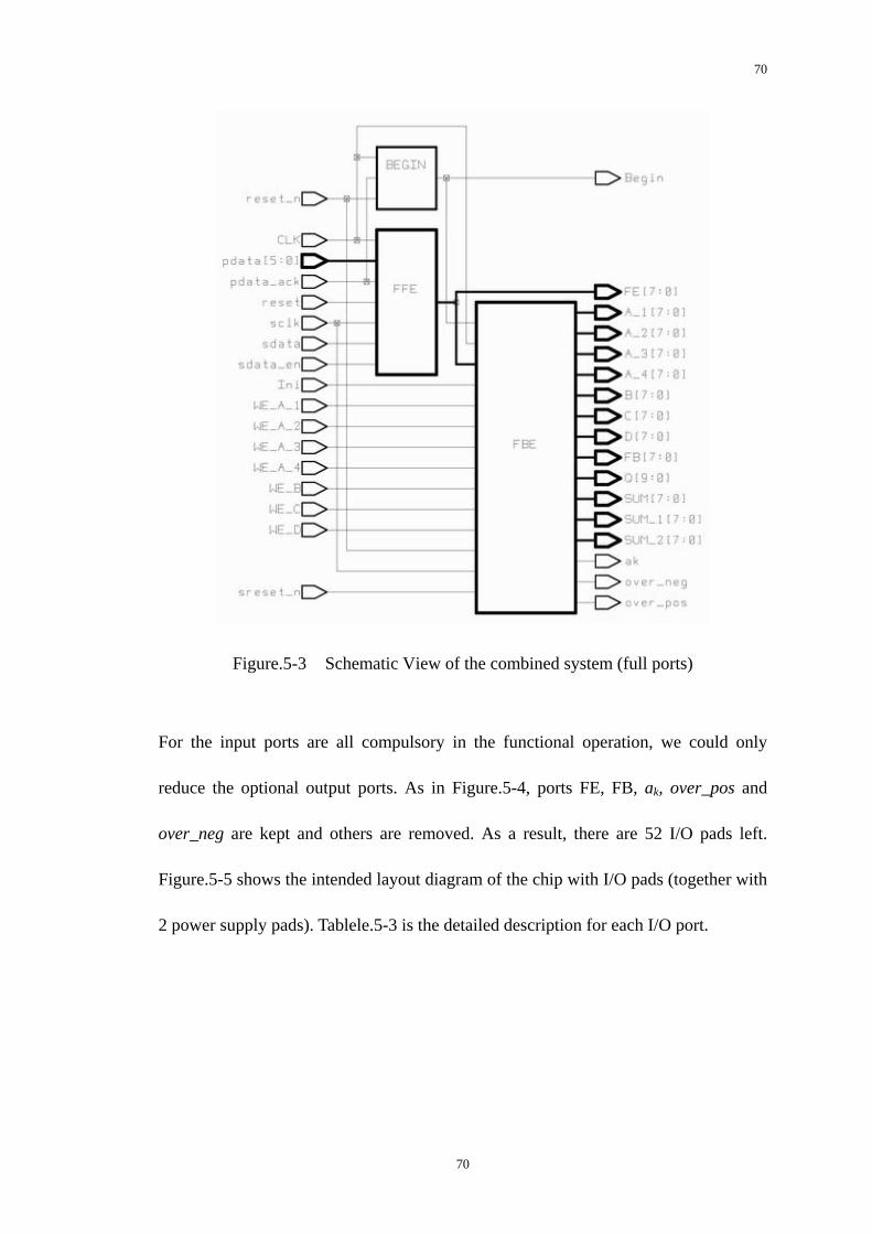
70
Figure.5-3 Schematic View of the combined system (full ports)
For the input ports are all compulsory in the functional operation, we could only
reduce the optional output ports. As in Figure.5-4, ports FE, FB, ak, over_pos and
over_neg are kept and others are removed. As a result, there are 52 I/O pads left.
Figure.5-5 shows the intended layout diagram of the chip with I/O pads (together with
2 power supply pads). Tablele.5-3 is the detailed description for each I/O port.
70
71
Figure.5-4 Schematic View of the combined system (partial ports)
71
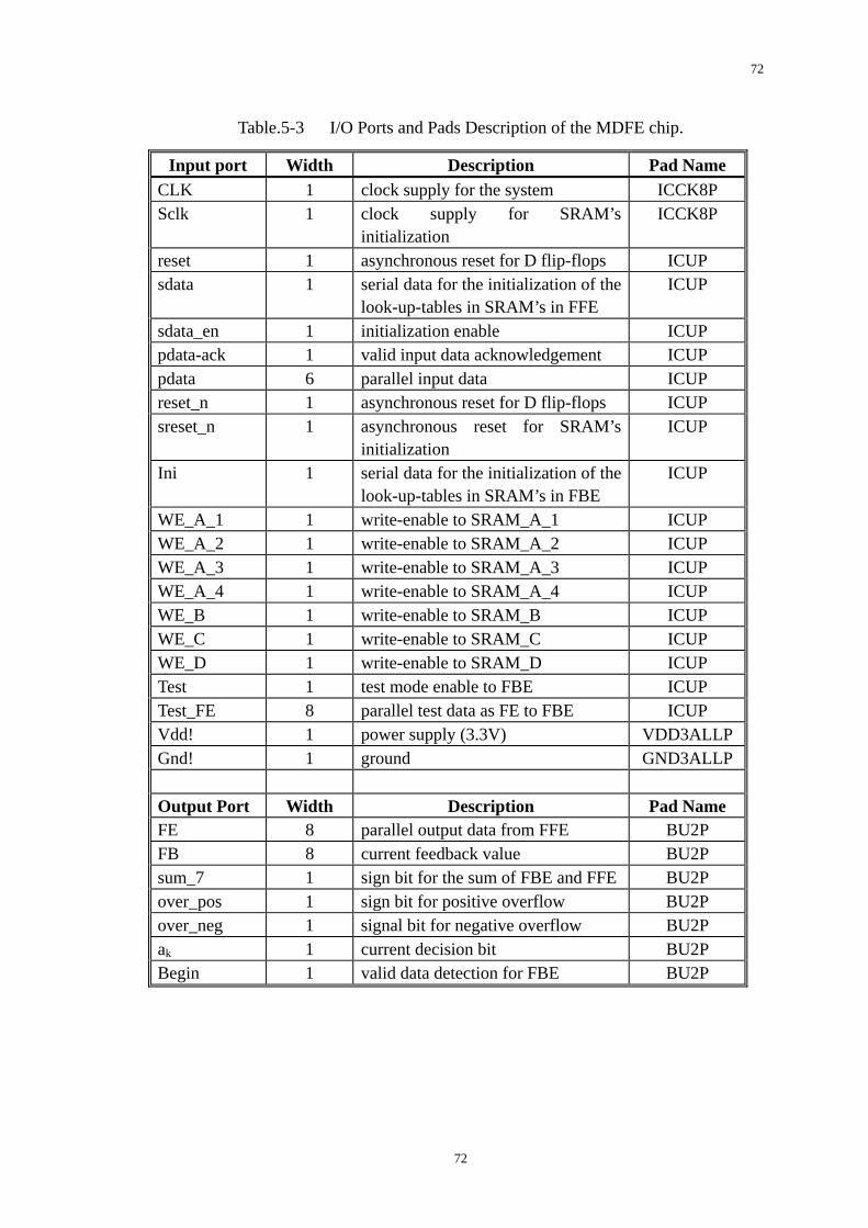
72
Table.5-3 I/O Ports and Pads Description of the MDFE chip.
Input port Width Description Pad Name CLK 1 clock supply for the system ICCK8P Sclk 1 clock supply for SRAM’s
initialization ICCK8P
reset 1 asynchronous reset for D flip-flops ICUP sdata 1 serial data for the initialization of the
look-up-tables in SRAM’s in FFE ICUP
sdata_en 1 initialization enable ICUP pdata-ack 1 valid input data acknowledgement ICUP pdata 6 parallel input data ICUP reset_n 1 asynchronous reset for D flip-flops ICUP sreset_n 1 asynchronous reset for SRAM’s
initialization ICUP
Ini 1 serial data for the initialization of the look-up-tables in SRAM’s in FBE
ICUP
WE_A_1 1 write-enable to SRAM_A_1 ICUP WE_A_2 1 write-enable to SRAM_A_2 ICUP WE_A_3 1 write-enable to SRAM_A_3 ICUP WE_A_4 1 write-enable to SRAM_A_4 ICUP WE_B 1 write-enable to SRAM_B ICUP WE_C 1 write-enable to SRAM_C ICUP WE_D 1 write-enable to SRAM_D ICUP Test 1 test mode enable to FBE ICUP Test_FE 8 parallel test data as FE to FBE ICUP Vdd! 1 power supply (3.3V) VDD3ALLPGnd! 1 ground GND3ALLP Output Port Width Description Pad Name FE 8 parallel output data from FFE BU2P FB 8 current feedback value BU2P sum_7 1 sign bit for the sum of FBE and FFE BU2P over_pos 1 sign bit for positive overflow BU2P over_neg 1 signal bit for negative overflow BU2P ak 1 current decision bit BU2P Begin 1 valid data detection for FBE BU2P
72
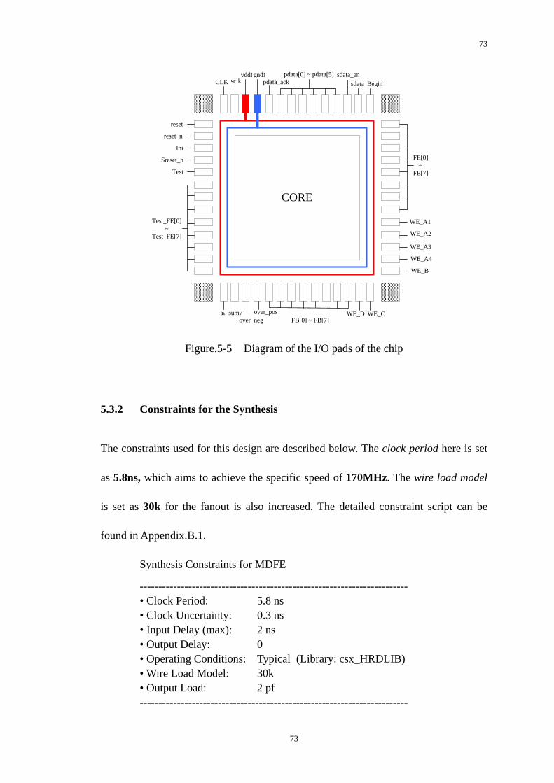
73
CORE
CLK sclkvdd!gnd!
pdata_ackpdata[0] ~ pdata[5] sdata_en
sdata
reset
reset_n
Ini
Sreset_n
Test
Test_FE[0]~
Test_FE[7]
FE[0]~
FE[7]
WE_A1
WE_A2
WE_A3
WE_A4
WE_B
ak WE_CWE_DFB[0] ~ FB[7]over_neg
over_possum7
Begin
Figure.5-5 Diagram of the I/O pads of the chip
5.3.2 Constraints for the Synthesis
The constraints used for this design are described below. The clock period here is set
as 5.8ns, which aims to achieve the specific speed of 170MHz. The wire load model
is set as 30k for the fanout is also increased. The detailed constraint script can be
found in Appendix.B.1.
Synthesis Constraints for MDFE
------------------------------------------------------------------------ • Clock Period: 5.8 ns • Clock Uncertainty: 0.3 ns • Input Delay (max): 2 ns • Output Delay: 0 • Operating Conditions: Typical (Library: csx_HRDLIB) • Wire Load Model: 30k • Output Load: 2 pf ------------------------------------------------------------------------
73
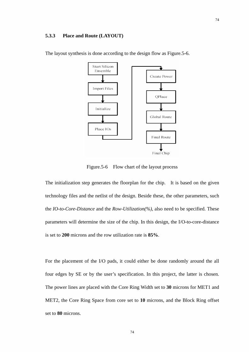
74
5.3.3 Place and Route (LAYOUT)
The layout synthesis is done according to the design flow as Figure.5-6.
Figure.5-6 Flow chart of the layout process
The initialization step generates the floorplan for the chip. It is based on the given
technology files and the netlist of the design. Beside these, the other parameters, such
the IO-to-Core-Distance and the Row-Utilization(%), also need to be specified. These
parameters will determine the size of the chip. In this design, the I/O-to-core-distance
is set to 200 microns and the row utilization rate is 85%.
For the placement of the I/O pads, it could either be done randomly around the all
four edges by SE or by the user’s specification. In this project, the latter is chosen.
The power lines are placed with the Core Ring Width set to 30 microns for MET1 and
MET2, the Core Ring Space from core set to 10 microns, and the Block Ring offset
set to 80 microns.
74
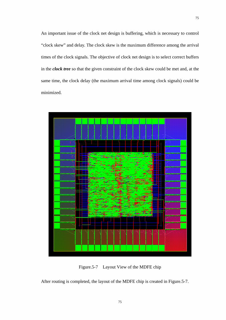
75
An important issue of the clock net design is buffering, which is necessary to control
“clock skew” and delay. The clock skew is the maximum difference among the arrival
times of the clock signals. The objective of clock net design is to select correct buffers
in the clock tree so that the given constraint of the clock skew could be met and, at the
same time, the clock delay (the maximum arrival time among clock signals) could be
minimized.
Figure.5-7 Layout View of the MDFE chip
After routing is completed, the layout of the MDFE chip is created in Figure.5-7.
75
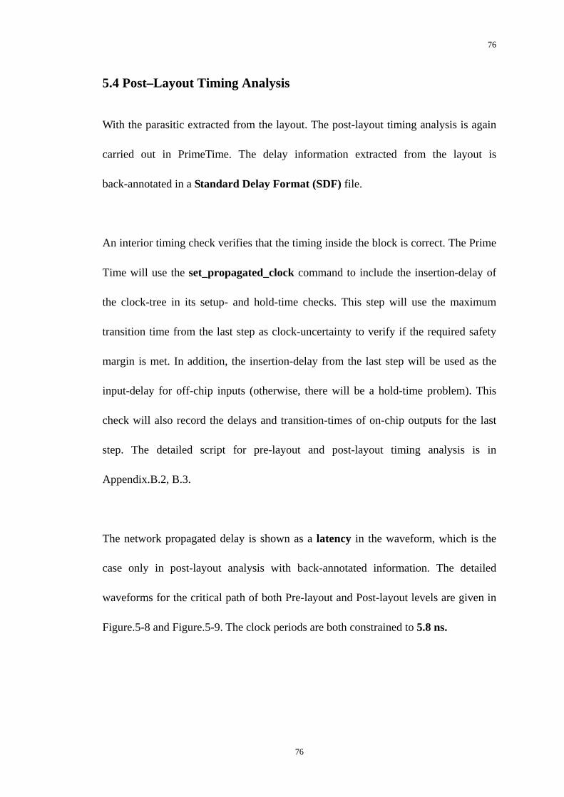
76
5.4 Post–Layout Timing Analysis
With the parasitic extracted from the layout. The post-layout timing analysis is again
carried out in PrimeTime. The delay information extracted from the layout is
back-annotated in a Standard Delay Format (SDF) file.
An interior timing check verifies that the timing inside the block is correct. The Prime
Time will use the set_propagated_clock command to include the insertion-delay of
the clock-tree in its setup- and hold-time checks. This step will use the maximum
transition time from the last step as clock-uncertainty to verify if the required safety
margin is met. In addition, the insertion-delay from the last step will be used as the
input-delay for off-chip inputs (otherwise, there will be a hold-time problem). This
check will also record the delays and transition-times of on-chip outputs for the last
step. The detailed script for pre-layout and post-layout timing analysis is in
Appendix.B.2, B.3.
The network propagated delay is shown as a latency in the waveform, which is the
case only in post-layout analysis with back-annotated information. The detailed
waveforms for the critical path of both Pre-layout and Post-layout levels are given in
Figure.5-8 and Figure.5-9. The clock periods are both constrained to 5.8 ns.
76
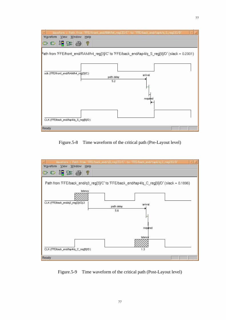
77
Figure.5-8 Time waveform of the critical path (Pre-Layout level)
Figure.5-9 Time waveform of the critical path (Post-Layout level)
77
78
In Figure.5-8, it reports the longest path (critical path) in Pre-Layout level as:
Startpoint: FFE / front_end / RAM/h4_reg[3] / C
Endpoint: FFE / back_end / tap4 / q_S_reg[9] / D
Slack: 0.2001 ns (MET)
In Figure.5-7-(b), it reports the critical path in Post-Layout level as:
Startpoint: FFE / back_end / q3_reg[3] / C
Endpoint: FFE / back_end / tap4 / q_C_reg[9] / D
Slack: 0.1896 ns (MET)
Network propagated delay (Latency): 1.3 ns
From the comparison above, we could get that there is no obvious change on the clock
rate even after layout process, though network propagated delay is added. This could
be explained by the proper estimated constraints set in the synthesis process, such as
wire-load-model, clock-skew, and input-delay.
Since the clock period is constrained to 5.8ns and the slack is positive and thus meets
the specification. The final MDFE at post-layout level could run at the speed of
170MHz. The summary of the final specifications attained is given in Table.5-4, and
the detailed reports of timing, area, and dynamic power could be found in
Appendix.B4, B5, and B6.
78
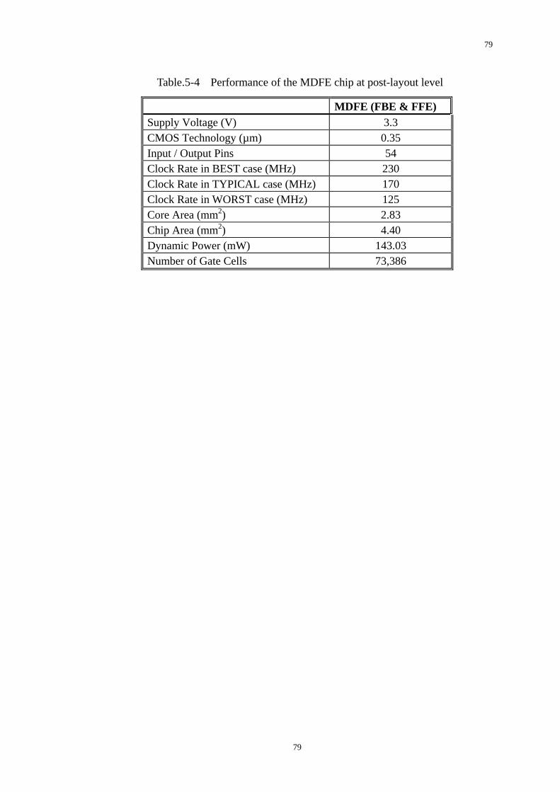
79
Table.5-4 Performance of the MDFE chip at post-layout level
MDFE (FBE & FFE) Supply Voltage (V) 3.3 CMOS Technology (µm) 0.35 Input / Output Pins 54 Clock Rate in BEST case (MHz) 230 Clock Rate in TYPICAL case (MHz) 170 Clock Rate in WORST case (MHz) 125 Core Area (mm2) 2.83 Chip Area (mm2) 4.40 Dynamic Power (mW) 143.03 Number of Gate Cells 73,386
79
80
Chapter 6 Conclusion
A fully digital MDFE chip that consists of an 8-tap feedback equalizer (FBE) and a
10-tap feed-forward equalizer (FFE) has been successfully designed and implemented
to the post-layout level. The FBE is implemented with the lookup-table based
architecture that consists of five 22×8-bit and three 23×8-bit SRAMs as the LUTs.
The past decisions are used to address the LUTs to form a decision feedback critical
loop. A number of architectures for FBE have been investigated and compared, from
which the final architecture is chosen. Three pipelined stages have been employed
to relax the timing constraints. The chip area has been greatly reduced by splitting
the large SRAM into small ones. The FFE has been implemented as a transposed filter.
In its architecture, the multipliers are of parallel array type that uses radix-4 modified
Booth encoding and a carry save partial product reduction scheme. An 8×8-bit
SRAM is used to store the 8-tap coefficients. Both the FBE and FFE are made
programmable.
Based on a 0.35µm CMOS technology, the synthesized FBE and FFE at post layout
level are capable of functioning up to 200MHz and 185MHz, respectively. For the
integrated MDFE chip, the clock rate has achieved 170MHz in TYPICAL case,
230MHz in BEST case, and 125MHz in WORST case. Further improvement needs to
be made to meet the specification of 150 MHz under the worst-case condition. The
80
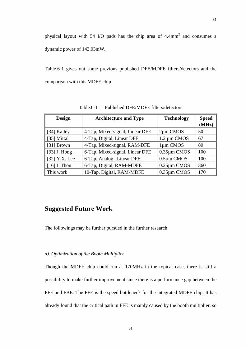
81
physical layout with 54 I/O pads has the chip area of 4.4mm2 and consumes a
dynamic power of 143.03mW.
Table.6-1 gives out some previous published DFE/MDFE filters/detectors and the
comparison with this MDFE chip.
Table.6-1 Published DFE/MDFE filters/detectors
Design Architecture and Type Technology Speed(MHz)
[34] Kajley 4-Tap, Mixed-signal, Linear DFE 2µm CMOS 50 [35] Mittal 4-Tap, Digital, Linear DFE 1.2 µm CMOS 67 [31] Brown 4-Tap, Mixed-signal, RAM-DFE 1µm CMOS 80 [33] J. Hong 6-Tap, Mixed-signal, Linear DFE 0.35µm CMOS 100 [32] Y.X. Lee 6-Tap, Analog , Linear DFE 0.5µm CMOS 100 [16] L.Thon 6-Tap, Digital, RAM-MDFE 0.25µm CMOS 360 This work 10-Tap, Digital, RAM-MDFE 0.35µm CMOS 170
Suggested Future Work
The followings may be further pursued in the further research:
a). Optimization of the Booth Multiplier
Though the MDFE chip could run at 170MHz in the typical case, there is still a
possibility to make further improvement since there is a performance gap between the
FFE and FBE. The FFE is the speed bottleneck for the integrated MDFE chip. It has
already found that the critical path in FFE is mainly caused by the booth multiplier, so
81
82
the optimization for the booth multiplier should be carried out. Furthermore, the
investigation for the more proper multiplier can also be considered.
b) Improvement on the worst-case performance
To improve the speed on worst-case, a direct solution is adopting a more advanced
CMOS technology such as 0.25µm or 0.18µm. By this means the speed could be
improved significantly. However, when technology is specific, a possible solution
that could be used to improve the speed is to “set multiple constraints” on the design.
Once the critical path is found through timing analysis, it can be re-syntheszed with a
special “worst-case constraint”. Other means such as investigation of different
architectures may also be considered.
82
83
REFERENCES
[1] K. A. Schouhamer Immink, “Run-length limited sequences,” Proceedings of
the IEEE, pp. 1745-1759, Nov. 1990.
[2] P.H. Seigel, “Recording codes for digital magnetic storage,” IEEE Trans.
Magn., vol. MAG-21, no. 5, pp. 1344-1349, Sept. 1985.
[3] R.W.Wood and D.A.Petersen, “Viterbi detection of Class-IV partial response
on a magnetic recording channel,” IEEE Trans. Commun., vol. COM-34, pp.
454–461, May 1986.
[4] R. D. Cideciyan, F. Dolivo, R. Hermann, W. Hirt, and W. Schott, “A PRML
system for digital magnetic recording,” IEEE J. Select. Areas Commun., vol.
10, pp. 38–56, Jan. 1992.
[5] A. M. Patel, “A new digital processing channel for data storage products,”
IEEE Trans. Magn., vol. 27, pp. 4579–4584, Nov. 1991.
[6] H. K. Thapar and A. M. Patel, “A class of partial response systems for
increasing storage density in magnetic recording,” IEEE Trans. Magn., vol.
23, pp. 3666–3668, Sept. 1987.
[7] J. J. Moon and L.R.Carley, “Performance comparison of detection methods
in magnetic recording,” IEEE Trans. Magn.,vol.26, pp.3155–3172, Nov.1990
83
84
[8] K. D. Fisher, J. M. Cioffi, W. L. Abbot, P. S. Bednarz, and C. M. Melas, “An
adaptive RAM-DFE for storage channels,” IEEE Trans. Commun., vol. 39,
pp. 1559–1568, Nov. 1991.
[9] J. G. Kenney, L. R. Carley, and R. W. Wood, “Multi-level decision feedback
equalization for saturation recording,” IEEE Trans. Magn., vol.29, pp.
2160–2171, July 1993.
[10] Brickner, B. and J. Moon, “A high dimensional signal space implementation
of FDTS/DF,” IEEE Trans. on Magn, vol. 32, no. 5, Sept., 1996
[11] Brickner, B. and J. Moon, “A signal space representation of fixed delay tree
search for use with d=0 codes,” Proc. of GLOBECOM ‘95, pp. 577-581 Nov.,
1995
[12] C.A. Belifiore and J.H. Park, Jr., "Decision Feedback Equalization," IEEE,
vol. 67, No. 8, pp. 1143-1155, Aug. 1979.
[13] J.G. Kenney and R. Wood, “ Multi-Level Decision Feedback Equalization:
An Effective Realization of FDTS/DF”, IEEE Trans. Magn., vol 31, pp
1115-1120, March 1995.
[14] P.S. Bednarz, S.C. Lin, C.S. Modlin and J.M. Cioffi, “Design, Performance,
and Extensions of the RAM-DFE Architecture,” IEEE Trans. Magn., vol 31,
pp 1196-1201, March, 1995.
[15] J.G. Kenney and C.M. Melas, “A Parallel Architecture for Multilevel
Decision Feedback Equalization,” IEEE Trans. Magn., vol 34, pp 588-595,
March 1998.
84
85
[16] L.Thon, “540MHz 21mW MDFE Equalizer and Detector in 0.25µm CMOS”,
ISSCC, 1998.
[17] George Mathew, B.Farhang-Boroujeny and R.W.Wood, “Design of
multilevel decision feedback equalizer”, IEEE Trans. Magn., Vol.33, No.6,
pp.4528-4542, Nov.1997.
[18] J. G.. Kenney and M. Melas, “Pipelining for Speed Doubling in MDFE,”
IEEE Trans. Magn., pp 561-565, 1996.
[19] L. P. Rubinfield, “A proof of the modified Booth’s algorithm for
multiplication”, IEEE Trans. Comput., Vol. C-24, pp. 1014-1015, October
1975.
[20] A. Oppenheim and R. Schafer, “Digital signal processing”, Eaglewood Cliffs,
NJ: Prentice-Hall, pp. 153-155, 1975.
[21] O. Salomon, J.-M. Green and H. Klar, “General algorithm for a simplified
addition of 2’s complement numbers in multipliers”, IEEE J. of Solid-state
circuits, Vol. 30, pp. 839-844, July 1995.
[22] C. R. Baugh and B. A. Wooley, “A two’s complementary parallel array
multiplication algorithm”, IEEE Trans. Comput., Vol. C-22, pp. 1045-1047,
December 1973.
[23] Alan Y. Kwentus, Hing-Tsun Hung, and Alan N. Willson, “An Architecture
for High-Performance/Small-Area Multipliers for Use in Digital Filtering
Applications”, IEEE Journal of solid-state circuits, Vol. 29.No.2 Feb. 1994.
[24] “Verilog-XL Reference Manual”, Cadence Design System.
85
86
[25] “NC Verilog Reference Manual”, Cadence Design System.
[26] “Design Compiler User Guide”, Synopsys Inc.
[27] “Design Compiler Reference Manual:Constraints and Timing” Synopsys Inc.
[29] “Design Compiler Reference Manual: Optimization and Timing Analysis”
Synopsys Inc.
[29] “PrimeTime User Guide”, Synopsys Inc.
[30] “Silicon Ensemble Reference Manual”, Cadence Design System.
[31] Brown, J., et al., “An 80Mb/s Adaptive DFE Detector in 1um CMOS,”
ISSCC Digest of Technical Papers, pp. 324-325, Feb., 1997.
[32] Y. X. Lee, etc., “Design, implementation, and performance evaluations of an
MDFE read channel” IEEE Trans. Magn., Vol.34, No.1, pp.166-171, Jan.,
1998.
[33] J. Hong, Y. X. Lee, H. Mutoh, “An Experimental MDFE Detector”, IEEE
Trans. On Magn., Vol.33, No.5, pp.2776-2778, Sept. 1997.
[34] Kajley, R., P. Hurst, J. Brown, “A Mixed-Signal Decision Feedback
Equalizer that uses a Look-Ahead Architecture,” J. Solid-State Circuits, pp.
450-459, Mar., 1997.
[35] Mittal, R., et al., “A Low-Power Backward Equalizer for DFE Read Channel
Applications,” J. Solid-State Circuits, pp. 270-273, Feb., 1997.
86
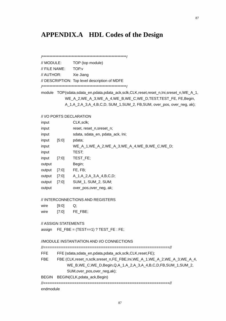
87
APPENDIX.A HDL Codes of the Design
/*********************************************************/ // MODULE: TOP (top module) // FILE NAME: TOP.v // AUTHOR: Xie Jiang // DESCRIPTION: Top level description of MDFE /*********************************************************/ module TOP (sdata,sdata_en,pdata,pdata_ack,sclk,CLK,reset,reset_n,Ini,sreset_n,WE_A_1, WE_A_2,WE_A_3,WE_A_4,WE_B,WE_C,WE_D,TEST,TEST_FE, FE,Begin,
A_1,A_2,A_3,A_4,B,C,D, SUM_1,SUM_2, FB,SUM, over_pos, over_neg, ak); // I/O PORTS DECLARATION input CLK,sclk; input reset, reset_n,sreset_n; input sdata, sdata_en, pdata_ack, Ini; input [5:0] pdata; input WE_A_1,WE_A_2,WE_A_3,WE_A_4,WE_B,WE_C,WE_D; input TEST; input [7:0] TEST_FE; output Begin; output [7:0] FE, FB; output [7:0] A_1,A_2,A_3,A_4,B,C,D; output [7:0] SUM_1, SUM_2, SUM; output over_pos,over_neg, ak; // INTERCONNECTIONS AND REGISTERS wire [9:0] Q; wire [7:0] FE_FBE; // ASSIGN STATEMENTS assign FE_FBE = (TEST==1) ? TEST_FE : FE; //MODULE INSTANTIATION AND I/O CONNECTIONS //=========================================================// FFE FFE (sdata,sdata_en,pdata,pdata_ack,sclk,CLK,reset,FE); FBE FBE (CLK,reset_n,sclk,sreset_n,FE_FBE,Ini,WE_A_1,WE_A_2,WE_A_3,WE_A_4,
WE_B,WE_C,WE_D,Begin,Q,A_1,A_2,A_3,A_4,B,C,D,FB,SUM_1,SUM_2, SUM,over_pos,over_neg,ak);
BEGIN BEGIN(CLK,pdata_ack,Begin) //=========================================================// endmodule
87
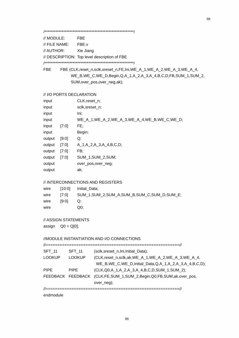
88
/*********************************************************/ // MODULE: FBE // FILE NAME: FBE.v // AUTHOR: Xie Jiang // DESCRIPTION: Top level description of FBE /*********************************************************/ FBE FBE (CLK,reset_n,sclk,sreset_n,FE,Ini,WE_A_1,WE_A_2,WE_A_3,WE_A_4,
WE_B,WE_C,WE_D,Begin,Q,A_1,A_2,A_3,A_4,B,C,D,FB,SUM_1,SUM_2, SUM,over_pos,over_neg,ak);
// I/O PORTS DECLARATION input CLK,reset_n; input sclk,sreset_n; input Ini; input WE_A_1,WE_A_2,WE_A_3,WE_A_4,WE_B,WE_C,WE_D; input [7:0] FE; input Begin; output [9:0] Q; output [7:0] A_1,A_2,A_3,A_4,B,C,D; output [7:0] FB; output [7:0] SUM_1,SUM_2,SUM; output over_pos,over_neg; output ak; // INTERCONNECTIONS AND REGISTERS wire [10:0] Initial_Data; wire [7:0] SUM_1,SUM_2,SUM_A,SUM_B,SUM_C,SUM_D,SUM_E; wire [9:0] Q; wire Q0; // ASSIGN STATEMENTS assign Q0 = Q[0]; //MODULE INSTANTIATION AND I/O CONNECTIONS //=========================================================// SFT_11 SFT_11 (sclk,sreset_n,Ini,Initial_Data); LOOKUP LOOKUP (CLK,reset_n,sclk,ak,WE_A_1,WE_A_2,WE_A_3,WE_A_4,
WE_B,WE_C,WE_D,Initial_Data,Q,A_1,A_2,A_3,A_4,B,C,D); PIPE PIPE (CLK,Q0,A_1,A_2,A_3,A_4,B,C,D,SUM_1,SUM_2); FEEDBACK FEEDBACK (CLK,FE,SUM_1,SUM_2,Begin,Q0,FB,SUM,ak,over_pos,
over_neg); //=========================================================// endmodule
88
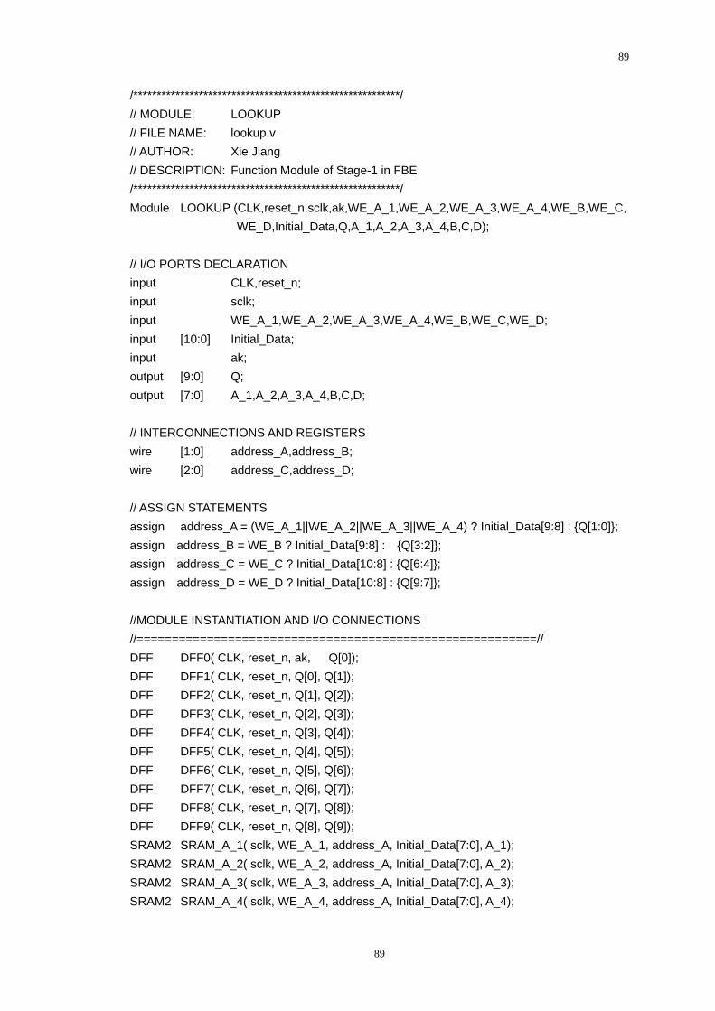
89
/*********************************************************/ // MODULE: LOOKUP // FILE NAME: lookup.v // AUTHOR: Xie Jiang // DESCRIPTION: Function Module of Stage-1 in FBE /*********************************************************/ Module LOOKUP (CLK,reset_n,sclk,ak,WE_A_1,WE_A_2,WE_A_3,WE_A_4,WE_B,WE_C, WE_D,Initial_Data,Q,A_1,A_2,A_3,A_4,B,C,D); // I/O PORTS DECLARATION input CLK,reset_n; input sclk; input WE_A_1,WE_A_2,WE_A_3,WE_A_4,WE_B,WE_C,WE_D; input [10:0] Initial_Data; input ak; output [9:0] Q; output [7:0] A_1,A_2,A_3,A_4,B,C,D; // INTERCONNECTIONS AND REGISTERS wire [1:0] address_A,address_B; wire [2:0] address_C,address_D; // ASSIGN STATEMENTS assign address_A = (WE_A_1||WE_A_2||WE_A_3||WE_A_4) ? Initial_Data[9:8] : {Q[1:0]}; assign address_B = WE_B ? Initial_Data[9:8] : {Q[3:2]}; assign address_C = WE_C ? Initial_Data[10:8] : {Q[6:4]}; assign address_D = WE_D ? Initial_Data[10:8] : {Q[9:7]}; //MODULE INSTANTIATION AND I/O CONNECTIONS //=========================================================// DFF DFF0( CLK, reset_n, ak, Q[0]); DFF DFF1( CLK, reset_n, Q[0], Q[1]); DFF DFF2( CLK, reset_n, Q[1], Q[2]); DFF DFF3( CLK, reset_n, Q[2], Q[3]); DFF DFF4( CLK, reset_n, Q[3], Q[4]); DFF DFF5( CLK, reset_n, Q[4], Q[5]); DFF DFF6( CLK, reset_n, Q[5], Q[6]); DFF DFF7( CLK, reset_n, Q[6], Q[7]); DFF DFF8( CLK, reset_n, Q[7], Q[8]); DFF DFF9( CLK, reset_n, Q[8], Q[9]); SRAM2 SRAM_A_1( sclk, WE_A_1, address_A, Initial_Data[7:0], A_1); SRAM2 SRAM_A_2( sclk, WE_A_2, address_A, Initial_Data[7:0], A_2); SRAM2 SRAM_A_3( sclk, WE_A_3, address_A, Initial_Data[7:0], A_3); SRAM2 SRAM_A_4( sclk, WE_A_4, address_A, Initial_Data[7:0], A_4);
89
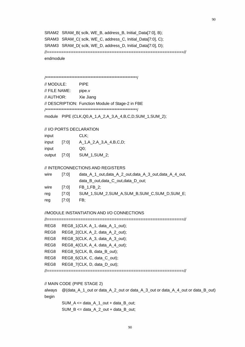
90
SRAM2 SRAM_B( sclk, WE_B, address_B, Initial_Data[7:0], B); SRAM3 SRAM_C( sclk, WE_C, address_C, Initial_Data[7:0], C); SRAM3 SRAM_D( sclk, WE_D, address_D, Initial_Data[7:0], D); //=========================================================// endmodule /*********************************************************/ // MODULE: PIPE // FILE NAME: pipe.v // AUTHOR: Xie Jiang // DESCRIPTION: Function Module of Stage-2 in FBE /*********************************************************/ module PIPE (CLK,Q0,A_1,A_2,A_3,A_4,B,C,D,SUM_1,SUM_2); // I/O PORTS DECLARATION input CLK; input [7:0] A_1,A_2,A_3,A_4,B,C,D; input Q0; output [7:0] SUM_1,SUM_2; // INTERCONNECTIONS AND REGISTERS wire [7:0] data_A_1_out,data_A_2_out,data_A_3_out,data_A_4_out,
data_B_out,data_C_out,data_D_out; wire [7:0] FB_1,FB_2; reg [7:0] SUM_1,SUM_2,SUM_A,SUM_B,SUM_C,SUM_D,SUM_E; reg [7:0] FB; //MODULE INSTANTIATION AND I/O CONNECTIONS //=========================================================// REG8 REG8_1(CLK, A_1, data_A_1_out); REG8 REG8_2(CLK, A_2, data_A_2_out); REG8 REG8_3(CLK, A_3, data_A_3_out); REG8 REG8_4(CLK, A_4, data_A_4_out); REG8 REG8_5(CLK, B, data_B_out); REG8 REG8_6(CLK, C, data_C_out); REG8 REG8_7(CLK, D, data_D_out); //=========================================================// // MAIN CODE (PIPE STAGE 2) always @(data_A_1_out or data_A_2_out or data_A_3_out or data_A_4_out or data_B_out) begin SUM_A <= data_A_1_out + data_B_out; SUM_B <= data_A_2_out + data_B_out;
90
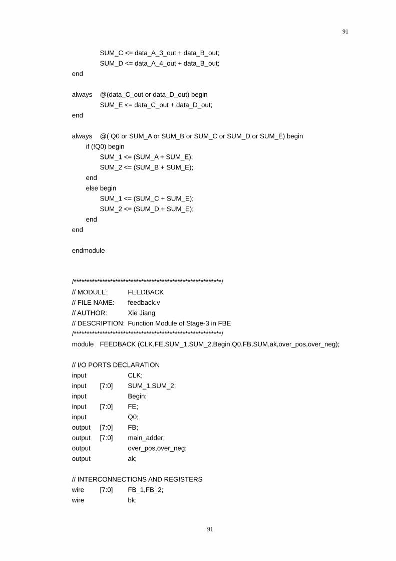
91
SUM_C <= data_A_3_out + data_B_out; SUM_D <= data_A_4_out + data_B_out; end always @(data_C_out or data_D_out) begin SUM_E <= data_C_out + data_D_out; end always @( Q0 or SUM_A or SUM_B or SUM_C or SUM_D or SUM_E) begin if (!Q0) begin SUM_1 <= (SUM_A + SUM_E); SUM_2 <= (SUM_B + SUM_E); end else begin SUM_1 <= (SUM_C + SUM_E); SUM_2 <= (SUM_D + SUM_E); end end endmodule /*********************************************************/ // MODULE: FEEDBACK // FILE NAME: feedback.v // AUTHOR: Xie Jiang // DESCRIPTION: Function Module of Stage-3 in FBE /*********************************************************/ module FEEDBACK (CLK,FE,SUM_1,SUM_2,Begin,Q0,FB,SUM,ak,over_pos,over_neg); // I/O PORTS DECLARATION input CLK; input [7:0] SUM_1,SUM_2; input Begin; input [7:0] FE; input Q0; output [7:0] FB; output [7:0] main_adder; output over_pos,over_neg; output ak; // INTERCONNECTIONS AND REGISTERS wire [7:0] FB_1,FB_2; wire bk;
91
92
reg [7:0] FB; reg [7:0] SUM; //MODULE INSTANTIATION AND I/O CONNECTIONS //=========================================================// REG8 REG8_8(CLK, SUM_1, FB_1); REG8 REG8_9(CLK, SUM_2, FB_2); //=========================================================// // MAIN CODE (PIPE STAGE 3) always @(Q0 or FB_1 or FB_2) begin if (!Q0) begin FB <= FB_1; end else begin FB <= FB_2; end end always @(FB or FE) begin SUM <= FE + FB; end // ASSIGN STATEMENTS assign over_pos = ((FE[7]==0) && (FB[7]==0) && (SUM[7]==1))? 1'b1:1'b0; assign over_neg = ((FE[7]==1) && (FB[7]==1) && (SUM[7]==0))? 1'b1:1'b0; assign bk = over_pos? 1'b0 : over_neg? 1'b1 : SUM[7]; assign ak = (Begin==1)? bk : FE[7]; endmodule /*********************************************************/ // MODULE: BEGIN // FILE NAME: begin.v // AUTHOR: Xie Jiang // DESCRIPTION: Delay Control Module in TOP /*********************************************************/ module BEGIN(CLK,reset_n,D,Q); // I/O PORTS DECLARATION input CLK; input D; output Q;
92
93
// INTERCONNECTIONS AND REGISTERS wire [9:0] q; // ASSIGN STATEMENTS assign Q = q[9]; //MODULE INSTANTIATION AND I/O CONNECTIONS //=========================================================// DFF D0(CLK, reset_n, D, q[0]); DFF D1(CLK, reset_n, q[0], q[1]); DFF D2(CLK, reset_n, q[1], q[2]); DFF D3(CLK, reset_n, q[2], q[3]); DFF D4(CLK, reset_n, q[3], q[4]); DFF D5(CLK, reset_n, q[4], q[5]); DFF D6(CLK, reset_n, q[5], q[6]); DFF D7(CLK, reset_n, q[6], q[7]); DFF D8(CLK, reset_n, q[7], q[8]); DFF D9(CLK, reset_n, q[8], q[9]); //=========================================================// endmodule
/*********************************************************/ // MODULE: SFT_11 // FILE NAME: sft_11.v // AUTHOR: Xie Jiang // DESCRIPTION: Serial to Parallel Converter /*********************************************************/ module SFT_11 (CLK,reset_n,Ini,Initial_Data); // I/O PORTS DECLARATION input CLK; input reset_n; input Ini; output [10:0] Initial_Data; //MODULE INSTANTIATION AND I/O CONNECTIONS //=========================================================// DFF D0(CLK, reset_n, Ini, Initial_Data[0]); DFF D1(CLK, reset_n, Initial_Data[0], Initial_Data[1]); DFF D2(CLK, reset_n, Initial_Data[1], Initial_Data[2]); DFF D3(CLK, reset_n, Initial_Data[2], Initial_Data[3]); DFF D4(CLK, reset_n, Initial_Data[3], Initial_Data[4]); DFF D5(CLK, reset_n, Initial_Data[4], Initial_Data[5]);
93
94
DFF D6(CLK, reset_n, Initial_Data[5], Initial_Data[6]); DFF D7(CLK, reset_n, Initial_Data[6], Initial_Data[7]); DFF D8(CLK, reset_n, Initial_Data[7], Initial_Data[8]); DFF D9(CLK, reset_n, Initial_Data[8], Initial_Data[9]); DFF D10(CLK, reset_n, Initial_Data[9], Initial_Data[10]); //=========================================================// endmodule /*********************************************************/ // MODULE: SRAM2 // FILE NAME: sram2.v // AUTHOR: Xie Jiang // DESCRIPTION: SRAM with 2-bit address /*********************************************************/ module SRAM2 (CLK, WE, address,data_in, data_out); // PARAMETERS parameter width = 8; parameter addr = 2; parameter depth = 4; // I/O PORTS DECLARATION input [width-1:0] data_in; input [addr-1:0] address; input CLK, WE; output [width-1:0] data_out; // INTERCONNECTIONS AND REGISTERS reg [width-1:0] mem [depth-1:0]; // ASSIGN STATEMENTS assign data_out = mem[address]; // MAIN CODE always @(posedge CLK) begin if(WE) mem[address] = data_in; end endmodule
94
95
/*********************************************************/ // MODULE: SRAM3 // FILE NAME: sram3.v // AUTHOR: Xie Jiang // DESCRIPTION: SRAM with 3-bit address /*********************************************************/ module SRAM3 (CLK, WE, address,data_in, data_out); // PARAMETERS parameter width = 8; parameter addr = 3; parameter depth = 8; // I/O PORTS DECLARATION input [width-1:0] data_in; input [addr-1:0] address; input CLK, WE; output [width-1:0] data_out; // INTERCONNECTIONS AND REGISTERS reg [width-1:0] mem [depth-1:0]; // ASSIGN STATEMENTS assign data_out = mem[address]; // MAIN CODE always @(posedge CLK) begin if(WE) mem[address] = data_in; end endmodule /*********************************************************/ // MODULE: REG8 // FILE NAME: reg8.v // AUTHOR: Xie Jiang // DESCRIPTION: Pipeline /*********************************************************/ module REG8 (CLK,data_in,data_out); // I/O PORTS DECLARATION input CLK;
95
96
input [7:0] data_in; output [7:0] data_out; //MODULE INSTANTIATION AND I/O CONNECTIONS //=========================================================// DFF8 D1(CLK, data_in[0], data_out[0]); DFF8 D2(CLK, data_in[1], data_out[1]); DFF8 D3(CLK, data_in[2], data_out[2]); DFF8 D4(CLK, data_in[3], data_out[3]); DFF8 D5(CLK, data_in[4], data_out[4]); DFF8 D6(CLK, data_in[5], data_out[5]); DFF8 D7(CLK, data_in[6], data_out[6]); DFF8 D8(CLK, data_in[7], data_out[7]); //=========================================================// endmodule /*********************************************************/ // MODULE: DFF // FILE NAME: dff.v // AUTHOR: Xie Jiang // DESCRIPTION: D-Flip-Flop with asynchronous reset /*********************************************************/ module DFF(CLK,reset_n,D,Q); // I/O PORTS DECLARATION input CLK; input reset_n; input D; output Q; // INTERCONNECTIONS AND REGISTERS reg Q; // MAIN CODE always @(posedge CLK or negedge reset_n) begin if(!reset_n) begin Q <= 1'b0; end else begin Q <= D; end end endmodule
96
97
/*********************************************************/ // MODULE: DFF8 // FILE NAME: dff8.v // AUTHOR: Xie Jiang // DESCRIPTION: D-Flip-Flop without reset /*********************************************************/ module DFF8 (CLK,D,Q); // I/O PORTS DECLARATION input CLK; input D; output Q; // INTERCONNECTIONS AND REGISTERS reg Q; // MAIN CODE always @(posedge CLK ) begin Q <= D; end endmodule
97
98
APPENDIX.B Scripts and Reports
B.1 Script of the Constraints for Synthesis
/****************************************************************/ current_design TOP; reset_design; #======================================# # Setting up the environment #======================================# set_operating_conditions -library csx_HRDLIB -max TYPICAL; set_wire_load_model –lib csx_HRLIB –name 30k set_load 2 all_outputs(); #======================================# # Setting up the timing assertions #======================================# create_clock -period 5.8 -name CLK find (port, CLK); set_dont_touch_network find (port, CLK); set_clock_uncertainty -setup 0.3 find (port, CLK); set_clock_uncertainty -hold 0.3 find (port, CLK); create_clock -period 5.8 -name sclk find (port, sclk); set_dont_touch_network find (port, sclk); set_clock_uncertainty -setup 0.3 find (port, sclk); set_clock_uncertainty -hold 0.3 find (port, sclk); #======================================# # Setting up the port delays #======================================# set_input_delay -max 2 -clock CLK find (port,pdata); set_input_delay -max 2 -clock CLK find (port,reset_n); remove_input_delay find (port,CLK); set_input_delay -max 2 -clock sclk find (port,sdata); set_input_delay -max 2 -clock sclk find (port,sdata_en); set_input_delay -max 2 -clock sclk find (port,pdata_ack); set_input_delay -max 2 -clock sclk find (port,reset); set_input_delay -max 2 -clock sclk find (port,Ini); set_input_delay -max 2 -clock sclk find (port,WE_A_1);
98
99
set_input_delay -max 2 -clock sclk find (port,WE_A_2); set_input_delay -max 2 -clock sclk find (port,WE_A_3); set_input_delay -max 2 -clock sclk find (port,WE_A_4); set_input_delay -max 2 -clock sclk find (port,WE_B); set_input_delay -max 2 -clock sclk find (port,WE_C); set_input_delay -max 2 -clock sclk find (port,WE_D); set_input_delay -max 2 -clock sclk find (port,sreset_n); remove_input_delay find (port,sclk);set_ output_delay –max 0 –clock all_outputs(); /****************************************************************/
B.2 Script of the Constraints for Pre-layout STA:
/****************************************************************/ current_design TOP reset_design #======================================# # Setting up the environment #======================================# set_operating_conditions -analysis_type single TYPICAL -library csx_HRDLIB set_wire_load_model -lib csx_HRDLIB -name 30k set_load 2 [all_outputs] #======================================# # Setting up the timing assertions #======================================# create_clock -period 5.8 -name CLK [get_ports CLK] set_dont_touch_network [get_ports CLK] set_clock_uncertainty -setup 0.3 [get_ports CLK] set_clock_uncertainty -hold 0.3 [get_ports CLK] create_clock -period 5.8 -name sclk [get_ports sclk] set_dont_touch_network [get_ports sclk] set_clock_uncertainty -setup 0.3 [get_ports sclk] set_clock_uncertainty -hold 0.3 [get_ports sclk] #======================================# # Setting up the port delays #======================================#
99
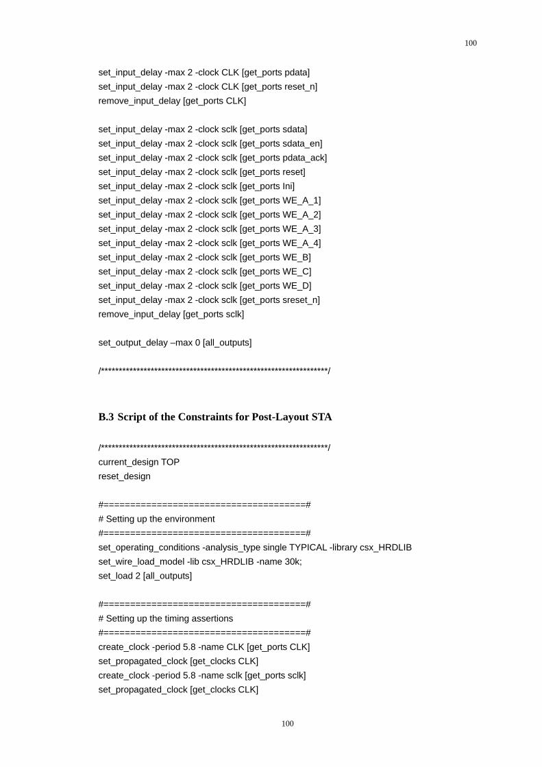
100
set_input_delay -max 2 -clock CLK [get_ports pdata] set_input_delay -max 2 -clock CLK [get_ports reset_n] remove_input_delay [get_ports CLK] set_input_delay -max 2 -clock sclk [get_ports sdata] set_input_delay -max 2 -clock sclk [get_ports sdata_en] set_input_delay -max 2 -clock sclk [get_ports pdata_ack] set_input_delay -max 2 -clock sclk [get_ports reset] set_input_delay -max 2 -clock sclk [get_ports Ini] set_input_delay -max 2 -clock sclk [get_ports WE_A_1] set_input_delay -max 2 -clock sclk [get_ports WE_A_2] set_input_delay -max 2 -clock sclk [get_ports WE_A_3] set_input_delay -max 2 -clock sclk [get_ports WE_A_4] set_input_delay -max 2 -clock sclk [get_ports WE_B] set_input_delay -max 2 -clock sclk [get_ports WE_C] set_input_delay -max 2 -clock sclk [get_ports WE_D] set_input_delay -max 2 -clock sclk [get_ports sreset_n] remove_input_delay [get_ports sclk] set_output_delay –max 0 [all_outputs] /****************************************************************/
B.3 Script of the Constraints for Post-Layout STA
/****************************************************************/ current_design TOP reset_design #======================================# # Setting up the environment #======================================# set_operating_conditions -analysis_type single TYPICAL -library csx_HRDLIB set_wire_load_model -lib csx_HRDLIB -name 30k; set_load 2 [all_outputs] #======================================# # Setting up the timing assertions #======================================# create_clock -period 5.8 -name CLK [get_ports CLK] set_propagated_clock [get_clocks CLK] create_clock -period 5.8 -name sclk [get_ports sclk] set_propagated_clock [get_clocks CLK]
100
101
read_sdf ./latest/TOP.sdf #======================================# # Setting up the port delays #======================================# set_input_delay -max 2 -clock CLK [get_ports pdata] set_input_delay -max 2 -clock CLK [get_ports reset_n] remove_input_delay [get_ports CLK] set_input_delay -max 2 -clock sclk [get_ports sdata] set_input_delay -max 2 -clock sclk [get_ports sdata_en] set_input_delay -max 2 -clock sclk [get_ports pdata_ack] set_input_delay -max 2 -clock sclk [get_ports reset] set_input_delay -max 2 -clock sclk [get_ports Ini] set_input_delay -max 2 -clock sclk [get_ports WE_A_1] set_input_delay -max 2 -clock sclk [get_ports WE_A_2] set_input_delay -max 2 -clock sclk [get_ports WE_A_3] set_input_delay -max 2 -clock sclk [get_ports WE_A_4] set_input_delay -max 2 -clock sclk [get_ports WE_B] set_input_delay -max 2 -clock sclk [get_ports WE_C] set_input_delay -max 2 -clock sclk [get_ports WE_D] set_input_delay -max 2 -clock sclk [get_ports sreset_n] remove_input_delay [get_ports sclk] set_output_delay –max 0 [all_outputs]
/****************************************************************/
B.4 Area Reports
**************************************** Report : area Design : FBE Version: 2001.08-SP2 Date : Fri Jun 18 14:58:51 2004 **************************************** Library(s) Used:csx_HRDLIB (File: /app23/AMS_3.40_CDS_F/synopsys/csx_3.3V/csx_HRDLIB.db) Number of ports: 105 Number of nets: 192 Number of cells: 64 Number of references: 7
101
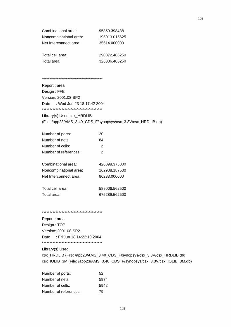
102
Combinational area: 95859.398438 Noncombinational area: 195013.015625 Net Interconnect area: 35514.000000 Total cell area: 290872.406250 Total area: 326386.406250
**************************************** Report : area Design : FFE Version: 2001.08-SP2 Date : Wed Jun 23 18:17:42 2004 **************************************** Library(s) Used:csx_HRDLIB (File: /app23/AMS_3.40_CDS_F/synopsys/csx_3.3V/csx_HRDLIB.db) Number of ports: 20 Number of nets: 84 Number of cells: 2 Number of references: 2 Combinational area: 426098.375000 Noncombinational area: 162908.187500 Net Interconnect area: 86283.000000 Total cell area: 589006.562500 Total area: 675289.562500
**************************************** Report : area Design : TOP Version: 2001.08-SP2 Date : Fri Jun 18 14:22:10 2004 **************************************** Library(s) Used: csx_HRDLIB (File: /app23/AMS_3.40_CDS_F/synopsys/csx_3.3V/csx_HRDLIB.db) csx_IOLIB_3M (File: /app23/AMS_3.40_CDS_F/synopsys/csx_3.3V/csx_IOLIB_3M.db) Number of ports: 52 Number of nets: 5974 Number of cells: 5942 Number of references: 79
102
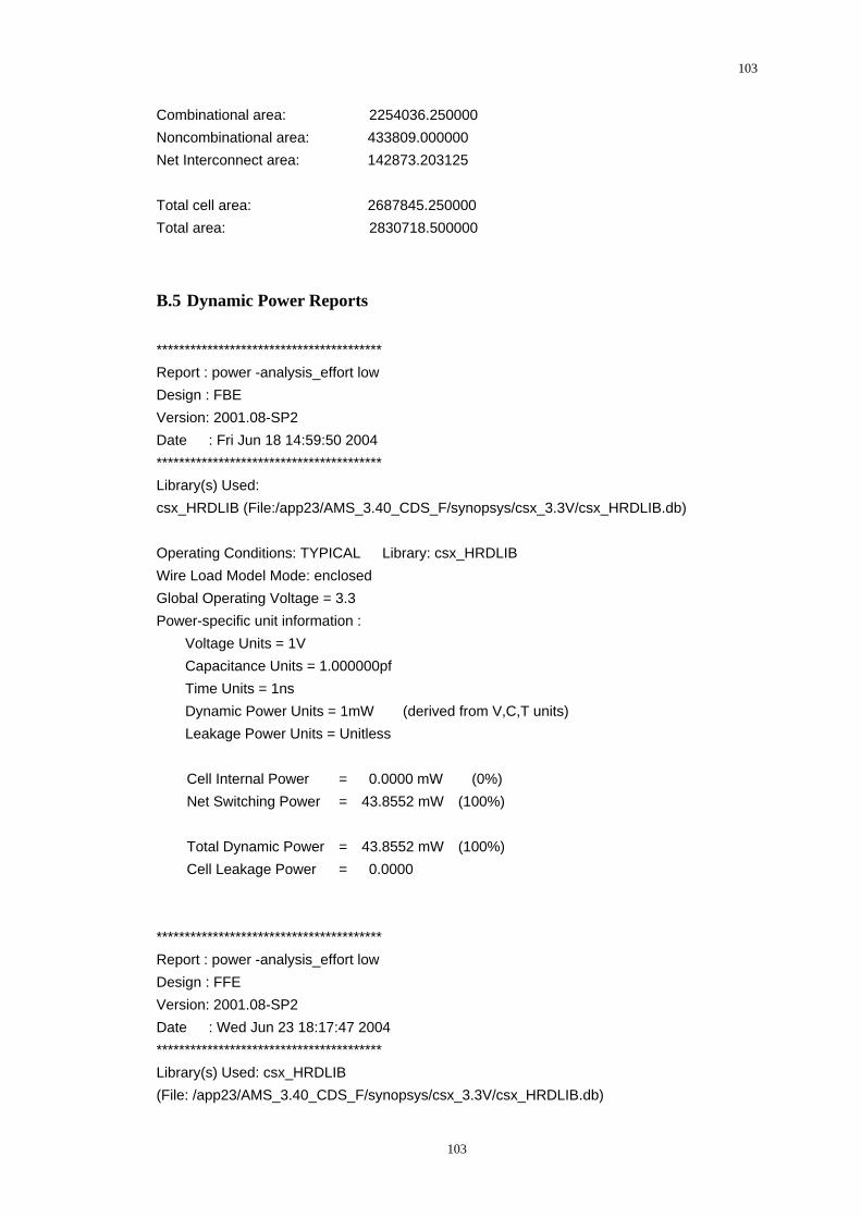
103
Combinational area: 2254036.250000 Noncombinational area: 433809.000000 Net Interconnect area: 142873.203125 Total cell area: 2687845.250000 Total area: 2830718.500000
B.5 Dynamic Power Reports
**************************************** Report : power -analysis_effort low Design : FBE Version: 2001.08-SP2 Date : Fri Jun 18 14:59:50 2004 **************************************** Library(s) Used: csx_HRDLIB (File:/app23/AMS_3.40_CDS_F/synopsys/csx_3.3V/csx_HRDLIB.db) Operating Conditions: TYPICAL Library: csx_HRDLIB Wire Load Model Mode: enclosed Global Operating Voltage = 3.3 Power-specific unit information : Voltage Units = 1V Capacitance Units = 1.000000pf Time Units = 1ns Dynamic Power Units = 1mW (derived from V,C,T units) Leakage Power Units = Unitless
Cell Internal Power = 0.0000 mW (0%) Net Switching Power = 43.8552 mW (100%)
Total Dynamic Power = 43.8552 mW (100%) Cell Leakage Power = 0.0000
**************************************** Report : power -analysis_effort low Design : FFE Version: 2001.08-SP2 Date : Wed Jun 23 18:17:47 2004 **************************************** Library(s) Used: csx_HRDLIB (File: /app23/AMS_3.40_CDS_F/synopsys/csx_3.3V/csx_HRDLIB.db)
103
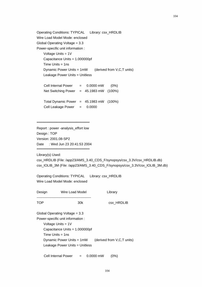
104
Operating Conditions: TYPICAL Library: csx_HRDLIB Wire Load Model Mode: enclosed Global Operating Voltage = 3.3 Power-specific unit information : Voltage Units = 1V Capacitance Units = 1.000000pf Time Units = 1ns Dynamic Power Units = 1mW (derived from V,C,T units) Leakage Power Units = Unitless Cell Internal Power = 0.0000 mW (0%) Net Switching Power = 45.1983 mW (100%)
Total Dynamic Power = 45.1983 mW (100%) Cell Leakage Power = 0.0000
**************************************** Report : power -analysis_effort low Design : TOP Version: 2001.08-SP2 Date : Wed Jun 23 20:41:53 2004 **************************************** Library(s) Used: csx_HRDLIB (File: /app23/AMS_3.40_CDS_F/synopsys/csx_3.3V/csx_HRDLIB.db) csx_IOLIB_3M (File: /app23/AMS_3.40_CDS_F/synopsys/csx_3.3V/csx_IOLIB_3M.db) Operating Conditions: TYPICAL Library: csx_HRDLIB Wire Load Model Mode: enclosed Design Wire Load Model Library ------------------------------------------------ TOP 30k csx_HRDLIB Global Operating Voltage = 3.3 Power-specific unit information : Voltage Units = 1V Capacitance Units = 1.000000pf Time Units = 1ns Dynamic Power Units = 1mW (derived from V,C,T units) Leakage Power Units = Unitless Cell Internal Power = 0.0000 mW (0%)
104
105
Net Switching Power = 143.0322 mW (100%) Total Dynamic Power = 143.0322 mW (100%) Cell Leakage Power = 0.0000
B.6 Timing Reports
**************************************** Report : timing -path full -delay max -max_paths 1 Design : FBE Version: 2001.08-SP2 Date : Wed Jun 23 20:01:54 2004 **************************************** Operating Conditions: TYPICAL Library: csx_HRDLIB Wire Load Model Mode: enclosed Startpoint: PIPE/REG8_4/D2/Q_reg (rising edge-triggered flip-flop clocked by CLK) Endpoint: FEEDBACK/REG8_9/D8/Q_reg (rising edge-triggered flip-flop clocked by CLK) Path Group: CLK Path Type: max Des/Clust/Port Wire Load Model Library -------------------------------------------------------------------------------------------------- FBE 10k csx_HRDLIB PIPE 10k csx_HRDLIB PIPE_DW01_add_8_3 10k csx_HRDLIB PIPE_DW01_add_8_0 10k csx_HRDLIB Point Incr Path --------------------------------------------------------------------------------------------------- clock CLK (rise edge) 0.00 0.00 clock network delay (ideal) 0.00 0.00 PIPE/REG8_4/D2/Q_reg/C (DF82) 0.00 0.00 r PIPE/REG8_4/D2/Q_reg/Q (DF82) 0.85 0.85 f PIPE/REG8_4/D2/Q (DFF8_46) 0.00 0.85 f PIPE/REG8_4/data_out[1] (REG8_5) 0.00 0.85 f PIPE/add_41/A[1] (PIPE_DW01_add_8_3) 0.00 0.85 f PIPE/add_41/U0_1_1/Q (NA22) 0.21 1.06 r PIPE/add_41/U19/Q (IN4) 0.06 1.12 f PIPE/add_41/U18/Q (AN21) 0.17 1.29 r PIPE/add_41/U25/Q (ON21) 0.18 1.47 f PIPE/add_41/U26/Q (IN4) 0.19 1.66 r PIPE/add_41/U1_4_2_3/Q (ON21) 0.18 1.84 f
105
106
PIPE/add_41/U21/Q (EO1) 0.36 2.20 f PIPE/add_41/SUM[4] (PIPE_DW01_add_8_3) 0.00 2.20 f PIPE/U37/Q (IMU22) 0.22 2.42 r PIPE/U59/Q (IN4) 0.07 2.49 f PIPE/r570_0/A[4] (PIPE_DW01_add_8_0) 0.00 2.49 f PIPE/r570_0/U12/Q (IN4) 0.10 2.59 r PIPE/r570_0/U11/Q (IN3) 0.08 2.67 f PIPE/r570_0/U0_1_4/Q (NA24) 0.12 2.78 r PIPE/r570_0/U26/Q (ON21) 0.14 2.92 f PIPE/r570_0/U1_4_1_6/Q (AN21) 0.22 3.14 r PIPE/r570_0/U1_4_2_6/Q (ON21) 0.17 3.31 f PIPE/r570_0/U27/Q (EN1) 0.44 3.75 f PIPE/r570_0/SUM[7] (PIPE_DW01_add_8_0) 0.00 3.75 f PIPE/U48/Q (IN3) 0.13 3.88 r PIPE/U71/Q (IMU24) 0.38 4.26 f PIPE/SUM_2[7] (PIPE) 0.00 4.26 f FEEDBACK/SUM_2[7] (FEEDBACK) 0.00 4.26 f FEEDBACK/REG8_9/data_in[7] (REG8_0) 0.00 4.26 f FEEDBACK/REG8_9/D8/D (DFF8_0) 0.00 4.26 f FEEDBACK/REG8_9/D8/Q_reg/D (DF8) 0.00 4.26 f data arrival time 4.26 clock CLK (rise edge) 5.00 5.00 clock network delay (ideal) 0.00 5.00 clock uncertainty -0.30 4.70 FEEDBACK/REG8_9/D8/Q_reg/C (DF8) 0.00 4.70 r library setup time -0.04 4.66 data required time 4.66 --------------------------------------------------------------------------------------------------- data required time 4.66 data arrival time -4.26 --------------------------------------------------------------------------------------------------- slack (MET) 0.40 **************************************** Report : timing -path full -delay max -max_paths 1 Design : FFE Version: 2001.08-SP2 Date : Wed Jun 23 18:17:49 2004 **************************************** Operating Conditions: TYPICAL Library: csx_HRDLIB Wire Load Model Mode: enclosed
106
107
Startpoint: front_end/RAM/h0_reg[1] (rising edge-triggered flip-flop clocked by sclk) Endpoint: back_end/tap0/q_S_reg[7] (rising edge-triggered flip-flop clocked by CLK) Path Group: CLK Path Type: max Des/Clust/Port Wire Load Model Library --------------------------------------------------------------------------------------------------- FFE 10k csx_HRDLIB bc_2 10k csx_HRDLIB booth_0 10k csx_HRDLIB fa_38 10k csx_HRDLIB fa_6 10k csx_HRDLIB bm_13 10k csx_HRDLIB tap_0 10k csx_HRDLIB fa_20 10k csx_HRDLIB Point Incr Path --------------------------------------------------------------------------------------------------- clock sclk (rise edge) 0.00 0.00 clock network delay (ideal) 0.00 0.00 front_end/RAM/h0_reg[1]/C (DFS84) 0.00 0.00 r front_end/RAM/h0_reg[1]/Q (DFS84) 0.68 0.68 f front_end/RAM/H0[1] (ram) 0.00 0.68 f front_end/h_0[1] (front 0.00 0.68 f back_end/h0[1] (fir) 0.00 0.68 f back_end/tap0/h[1] (tap_0) 0.00 0.68 f back_end/tap0/tap_booth/X[1] (booth_0) 0.00 0.68 f back_end/tap0/tap_booth/bc2/X_i (bc_2) 0.00 0.68 f back_end/tap0/tap_booth/bc2/U4/Q (EO1) 0.36 1.04 f back_end/tap0/tap_booth/bc2/U3/Q (IN4) 0.13 1.17 r back_end/tap0/tap_booth/bc2/U19/Q (INO22) 0.12 1.29 f back_end/tap0/tap_booth/bc2/One_N (bc_2) 0.00 1.29 f back_end/tap0/tap_booth/U11/Q (IN4) 0.14 1.43 r back_end/tap0/tap_booth/U20/Q (IN4) 0.06 1.49 f back_end/tap0/tap_booth/bm2_5/One_N (bm_13) 0.00 1.49 f back_end/tap0/tap_booth/bm2_5/U7/Q (IMU2) 0.25 1.74 f back_end/tap0/tap_booth/bm2_5/U2/Q (IMU2) 0.22 1.96 r back_end/tap0/tap_booth/bm2_5/U8/Q (INO22) 0.18 2.14 f back_end/tap0/tap_booth/bm2_5/out (bm_13) 0.00 2.14 f back_end/tap0/tap_booth/fa2_5/Cin (fa_38) 0.00 2.14 f back_end/tap0/tap_booth/fa2_5/U5/Q (IN4) 0.11 2.24 r back_end/tap0/tap_booth/fa2_5/U7/Q (AN22) 0.25 2.50 f back_end/tap0/tap_booth/fa2_5/Cout (fa_38) 0.00 2.50 f back_end/tap0/tap_booth/fa3_4/Cin (fa_34) 0.00 2.50 f
107
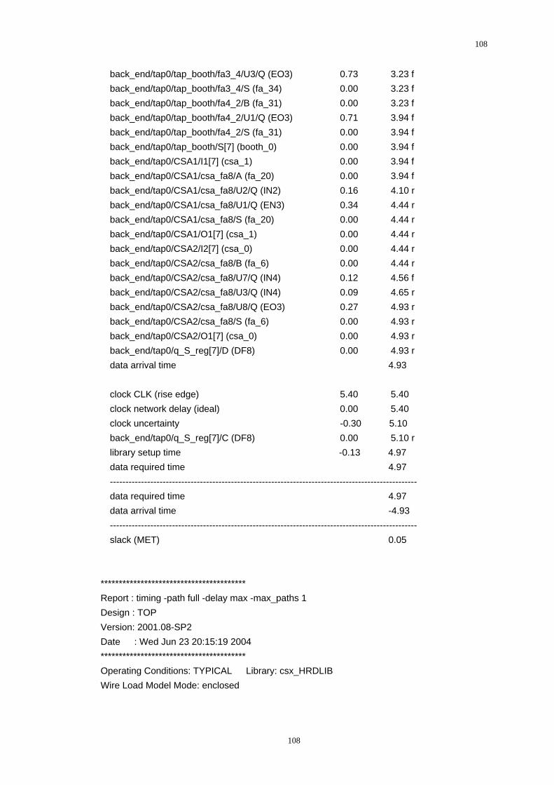
108
back_end/tap0/tap_booth/fa3_4/U3/Q (EO3) 0.73 3.23 f back_end/tap0/tap_booth/fa3_4/S (fa_34) 0.00 3.23 f back_end/tap0/tap_booth/fa4_2/B (fa_31) 0.00 3.23 f back_end/tap0/tap_booth/fa4_2/U1/Q (EO3) 0.71 3.94 f back_end/tap0/tap_booth/fa4_2/S (fa_31) 0.00 3.94 f back_end/tap0/tap_booth/S[7] (booth_0) 0.00 3.94 f back_end/tap0/CSA1/I1[7] (csa_1) 0.00 3.94 f back_end/tap0/CSA1/csa_fa8/A (fa_20) 0.00 3.94 f back_end/tap0/CSA1/csa_fa8/U2/Q (IN2) 0.16 4.10 r back_end/tap0/CSA1/csa_fa8/U1/Q (EN3) 0.34 4.44 r back_end/tap0/CSA1/csa_fa8/S (fa_20) 0.00 4.44 r back_end/tap0/CSA1/O1[7] (csa_1) 0.00 4.44 r back_end/tap0/CSA2/I2[7] (csa_0) 0.00 4.44 r back_end/tap0/CSA2/csa_fa8/B (fa_6) 0.00 4.44 r back_end/tap0/CSA2/csa_fa8/U7/Q (IN4) 0.12 4.56 f back_end/tap0/CSA2/csa_fa8/U3/Q (IN4) 0.09 4.65 r back_end/tap0/CSA2/csa_fa8/U8/Q (EO3) 0.27 4.93 r back_end/tap0/CSA2/csa_fa8/S (fa_6) 0.00 4.93 r back_end/tap0/CSA2/O1[7] (csa_0) 0.00 4.93 r back_end/tap0/q_S_reg[7]/D (DF8) 0.00 4.93 r data arrival time 4.93 clock CLK (rise edge) 5.40 5.40 clock network delay (ideal) 0.00 5.40 clock uncertainty -0.30 5.10 back_end/tap0/q_S_reg[7]/C (DF8) 0.00 5.10 r library setup time -0.13 4.97 data required time 4.97 --------------------------------------------------------------------------------------------------- data required time 4.97 data arrival time -4.93 --------------------------------------------------------------------------------------------------- slack (MET) 0.05 **************************************** Report : timing -path full -delay max -max_paths 1 Design : TOP Version: 2001.08-SP2 Date : Wed Jun 23 20:15:19 2004 **************************************** Operating Conditions: TYPICAL Library: csx_HRDLIB Wire Load Model Mode: enclosed
108
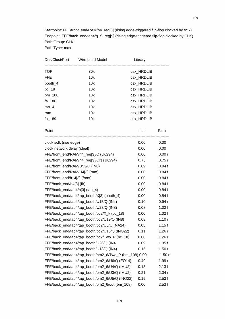
109
Startpoint: FFE/front_end/RAM/h4_reg[3] (rising edge-triggered flip-flop clocked by sclk) Endpoint: FFE/back_end/tap4/q_S_reg[9] (rising edge-triggered flip-flop clocked by CLK) Path Group: CLK Path Type: max Des/Clust/Port Wire Load Model Library --------------------------------------------------------------------------------------------------- TOP 30k csx_HRDLIB FFE 10k csx_HRDLIB booth_4 10k csx_HRDLIB bc_18 10k csx_HRDLIB bm_108 10k csx_HRDLIB fa_186 10k csx_HRDLIB tap_4 10k csx_HRDLIB ram 10k csx_HRDLIB fa_189 10k csx_HRDLIB Point Incr Path --------------------------------------------------------------------------------------------------- clock sclk (rise edge) 0.00 0.00 clock network delay (ideal) 0.00 0.00 FFE/front_end/RAM/h4_reg[3]/C (JKS94) 0.00 0.00 r FFE/front_end/RAM/h4_reg[3]/QN (JKS94) 0.75 0.75 r FFE/front_end/RAM/U53/Q (IN8) 0.09 0.84 f FFE/front_end/RAM/H4[3] (ram) 0.00 0.84 f FFE/front_end/h_4[3] (front) 0.00 0.84 f FFE/back_end/h4[3] (fir) 0.00 0.84 f FFE/back_end/tap4/h[3] (tap_4) 0.00 0.84 f FFE/back_end/tap4/tap_booth/X[3] (booth_4) 0.00 0.84 f FFE/back_end/tap4/tap_booth/U15/Q (IN4) 0.10 0.94 r FFE/back_end/tap4/tap_booth/U23/Q (IN8) 0.08 1.02 f FFE/back_end/tap4/tap_booth/bc2/X_k (bc_18) 0.00 1.02 f FFE/back_end/tap4/tap_booth/bc2/U19/Q (IN8) 0.08 1.10 r FFE/back_end/tap4/tap_booth/bc2/U5/Q (NA24) 0.05 1.15 f FFE/back_end/tap4/tap_booth/bc2/U16/Q (INO22) 0.11 1.26 r FFE/back_end/tap4/tap_booth/bc2/Two_P (bc_18) 0.00 1.26 r FFE/back_end/tap4/tap_booth/U26/Q (IN4 0.09 1.35 f FFE/back_end/tap4/tap_booth/U13/Q (IN4) 0.15 1.50 r FFE/back_end/tap4/tap_booth/bm2_6/Two_P (bm_108) 0.00 1.50 r FFE/back_end/tap4/tap_booth/bm2_6/U6/Q (EO14) 0.49 1.99 r FFE/back_end/tap4/tap_booth/bm2_6/U4/Q (IMU2) 0.13 2.13 f FFE/back_end/tap4/tap_booth/bm2_6/U3/Q (IMU2) 0.21 2.34 r FFE/back_end/tap4/tap_booth/bm2_6/U5/Q (INO22) 0.19 2.53 f FFE/back_end/tap4/tap_booth/bm2_6/out (bm_108) 0.00 2.53 f
109
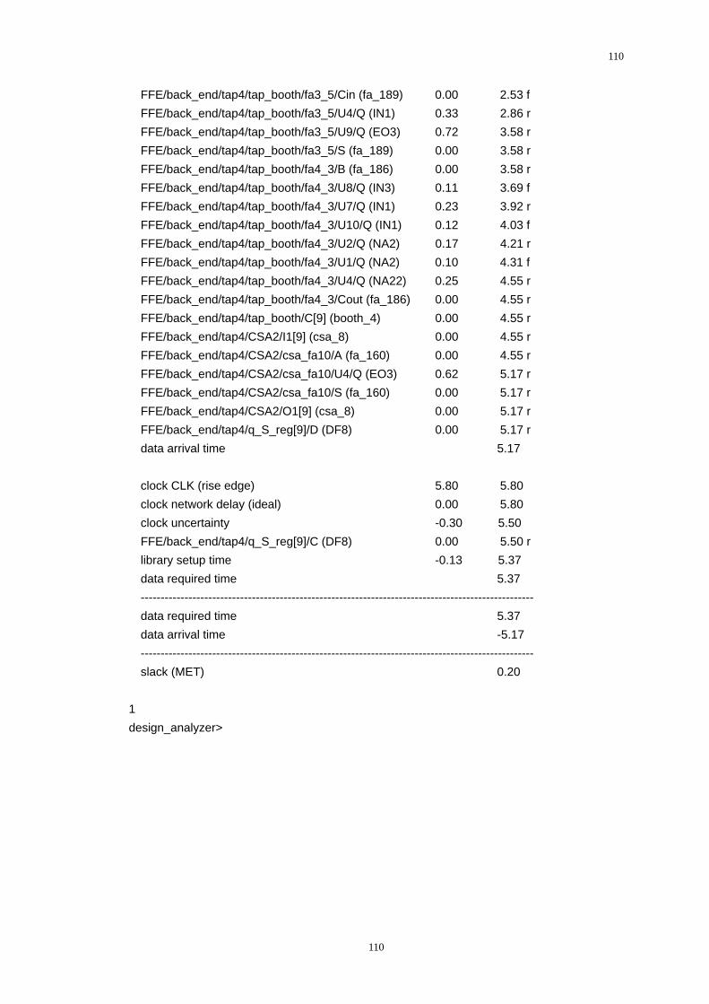
110
FFE/back_end/tap4/tap_booth/fa3_5/Cin (fa_189) 0.00 2.53 f FFE/back_end/tap4/tap_booth/fa3_5/U4/Q (IN1) 0.33 2.86 r FFE/back_end/tap4/tap_booth/fa3_5/U9/Q (EO3) 0.72 3.58 r FFE/back_end/tap4/tap_booth/fa3_5/S (fa_189) 0.00 3.58 r FFE/back_end/tap4/tap_booth/fa4_3/B (fa_186) 0.00 3.58 r FFE/back_end/tap4/tap_booth/fa4_3/U8/Q (IN3) 0.11 3.69 f FFE/back_end/tap4/tap_booth/fa4_3/U7/Q (IN1) 0.23 3.92 r FFE/back_end/tap4/tap_booth/fa4_3/U10/Q (IN1) 0.12 4.03 f FFE/back_end/tap4/tap_booth/fa4_3/U2/Q (NA2) 0.17 4.21 r FFE/back_end/tap4/tap_booth/fa4_3/U1/Q (NA2) 0.10 4.31 f FFE/back_end/tap4/tap_booth/fa4_3/U4/Q (NA22) 0.25 4.55 r FFE/back_end/tap4/tap_booth/fa4_3/Cout (fa_186) 0.00 4.55 r FFE/back_end/tap4/tap_booth/C[9] (booth_4) 0.00 4.55 r FFE/back_end/tap4/CSA2/I1[9] (csa_8) 0.00 4.55 r FFE/back_end/tap4/CSA2/csa_fa10/A (fa_160) 0.00 4.55 r FFE/back_end/tap4/CSA2/csa_fa10/U4/Q (EO3) 0.62 5.17 r FFE/back_end/tap4/CSA2/csa_fa10/S (fa_160) 0.00 5.17 r FFE/back_end/tap4/CSA2/O1[9] (csa_8) 0.00 5.17 r FFE/back_end/tap4/q_S_reg[9]/D (DF8) 0.00 5.17 r data arrival time 5.17 clock CLK (rise edge) 5.80 5.80 clock network delay (ideal) 0.00 5.80 clock uncertainty -0.30 5.50 FFE/back_end/tap4/q_S_reg[9]/C (DF8) 0.00 5.50 r library setup time -0.13 5.37 data required time 5.37 --------------------------------------------------------------------------------------------------- data required time 5.37 data arrival time -5.17 --------------------------------------------------------------------------------------------------- slack (MET) 0.20 1 design_analyzer>
110