Embed Size (px)
Citation preview
-R1-A5i 834 DESIGNING VLSI (VERY LARGE SCALE INTEGRATED) CIRCUITS 1/2FOR TESTRBILIT(J) AIR FORCE INST OF TECHIRIGHT-PATTERSON AFB OH SCHOOL OF ENGINEERING M KAPLAN
UNCLASSIFIED DEC 84 RFIT/GE/ENG/84D-39 F/G 9/5 ML
Ig
111.025112
NAIN WI' OF TArF2) 11" A.
RFPRnflLUJFD AT GOVERNMENtFXPENSE
00
i.(I
DESIGNING VLSI CIRCUITS
FOR TESTABILITY
THESIS
Michael Kaplan, B.E.E.Captain, USAF
AFIT/GE/ENG/84D-39
- ,, - , _ ., jVDTI Cl- w awedis G .1\ELECTE4: ¢,, , • .-,,.! \ APR 0 1 i98fi
DEPARTMENT OF THE AIR FORCE EAIR UNIVERSITY
AIR FORCE INSTITUTE OF TECHNOLOGY
Wright-Patterson Air Force Base, Ohio
. 03 13 087
* i,!- I -- .n ,.
DESIGNING VLSI CIRCUITS
FOR TESTABILITY
THESIS
Michael Kaplan, B.E.E.Captain, USAF
AF IT/GE/ENG/ 84D-3 9
AF IT/GE/ENG/84D-39
DESIGNING VLSI CIRCUITS FOR TESTABILITY
THESIS
Presented to the Faculty of the School of Engineering
of the Air Force Institute of Technology
Air University
In Partial Fulfillment of the
Requirements for the Degree of
Master of Science in Electrical Engineering
COPY-
Michael Kaplan, B.E.E.
Captain, USAF
r2
December 1984
As
Approved for public release; distribution unlimited
b-. 6: . .i i-" " o ; . _ ' - .

Preface
The purpose of this study was to investigate methods of
designing a circuit that would be highly testable when
completed. This subject is of great interest to the
government as well as private industry. The more testable a
circuit is, the more time and money can be saved once a
device is fabricated. It is for these reasons that I chose
this topic.
During this study, methods were examined to design
testable circuits, and were implemented in a design of my
own. Although not completely self-testing, the design
* should give you a feeling for the difficulty of designing
. such a circuit, and the ease of testing it.
In would like to thank my faculty advisor, Lt Col Harold
*W. Carter, for his assistance and guidance throughout this
effort. Also I would like to thank the Air Force Institute
of Technology library staff for their help. Finally, I wish
to thank my wife Cherie for her support and understanding
throughout these last 18 months.
M
Michael Kaplan
ii
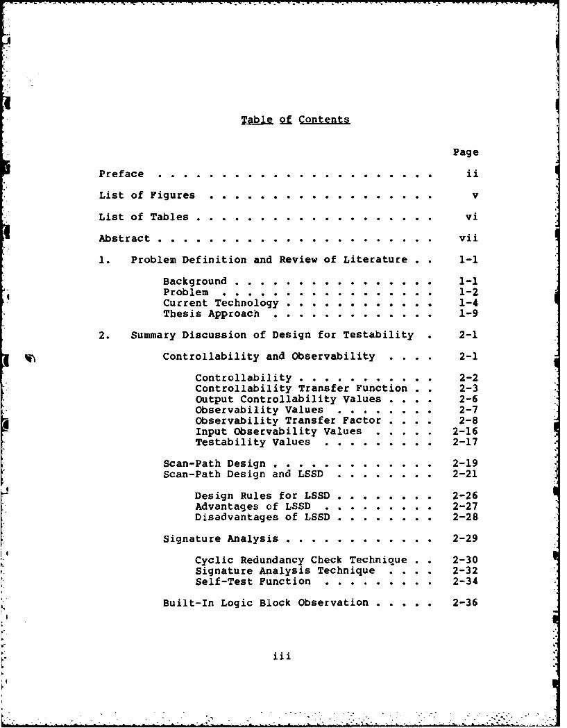
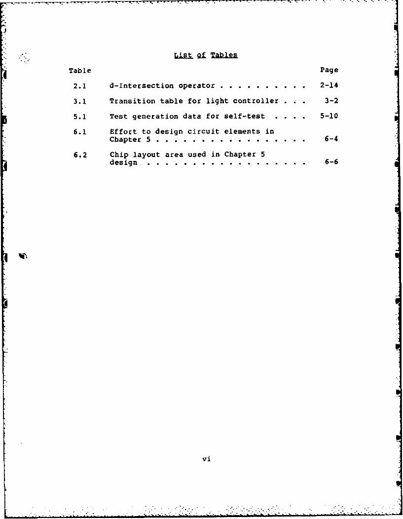
Table qf Contents
Page
Preface . . . . . . . . . . . . . . . . . . . . ii
List of Figures . . . . . . . . . . . . . .. . v
List of Tables . . . . . ........ . . . . . . . vi
Abstract . . . . . . . . . . . . . . . . . . . . . . vii
1. Problem Definition and Review of Literature . . 1-1
Background . . . . . . . . . . . . . . . . 1-1Problem. . ._...... . . . . . . . . 1-2CurrentTechnology . .. . ....... 1-4Thesis Approach . . . . . . . . . . . . . 1-9
2. Summary Discussion of Design for Testability . 2-1
Controllability and Observability . . . . 2-1
Controllability . . . . . . . . 2-2Controllability Transfer Function . 2-3Output Controllability Values . ... 2-6Observability Values . . . . .... 2-7Observability Transfer Factor . ... 2-8Input Observability Values ..... .. 2-16Testability Values . . . . . . 2-17
Scan-Path Design . . . . . . . . o . . . . 2-19Scan-Path Design and LSSD o . . . . . . . 2-21
Design Rules for LSSD . . . . . . . . 2-26Advantages of LSSD . . . . . . . . . 2-27Disadvantages of LSSD . . . . . . . . 2-28
Signature Analysis . . . o . . . . . . . . 2-29
Cyclic Redundancy Check Technique . . 2-30Signature Analysis Technique . . .. 2-32Self-Test Function .......... 2-34
Built-In Logic Block Observation . . . . . 2-36
iii
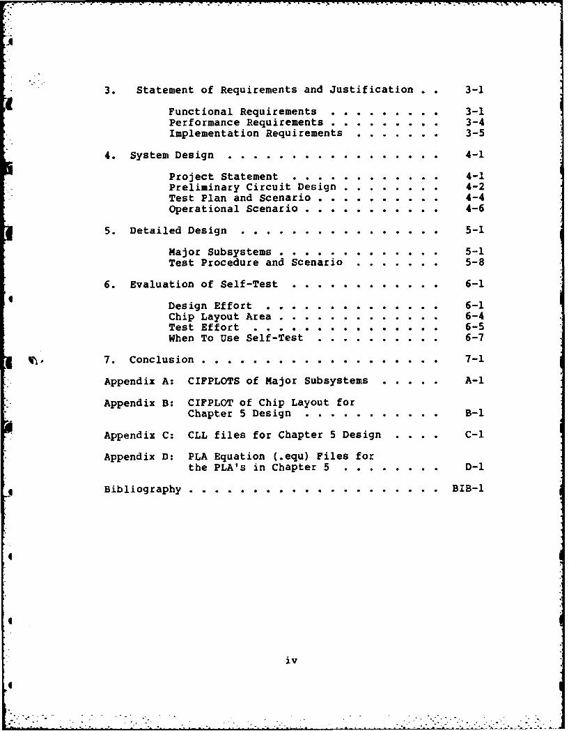
3. Statement of Requirements and Justification . . 3-1
Functional Requirements . . . .. . . . 3-1Performance Requirements . . . . . . . . . 3-4Implementation Requirements ........ . 3-5
4. System Design . . . . . . . . . . . . . . . . . 4-1
Project Statement . .*. . . . . . . . 4-1Preliminary Circuit Design ........ 4-2Test Plan and Scenario.......... 4-4Operational Scenario . . . . . . . . . . . 4-6
5. Detailed Design . . . ....... . . . . . . 5-1
Major Subsystems . . . . . . . . . . . 5-1Test Procedure and Scenario . .. . . . . 5-8
6. Evaluation of Self-Test ........ 6-1
Design Effort . . . . . . . . . . . . . . 6-1Chip Layout Area............. 6-4Test Effort . . . . . . . . . . . . . . . 6-5When To Use Self-Test....... . . . 6-7
7. Conclusion . . . . . . . . . . . . . . . . . . . 7-1
Appendix A: CIFPLOTS of Major Subsystems . . . . . A-1
Appendix B: CIFPLOT of Chip Layout forChapter 5 Design . . . . . . . . . . . B-i
Appendix C: CLL files for Chapter 5 Design . . . . C-1
Appendix D: PLA Equation (.equ) Files forthe PLA's in Chapter 5 . . . . . . . . D-1
Bibliography . . . . . . . . . . . . . . . . . . . . BIB-l
iv
[Ii: ' " . . .. . . . .'..
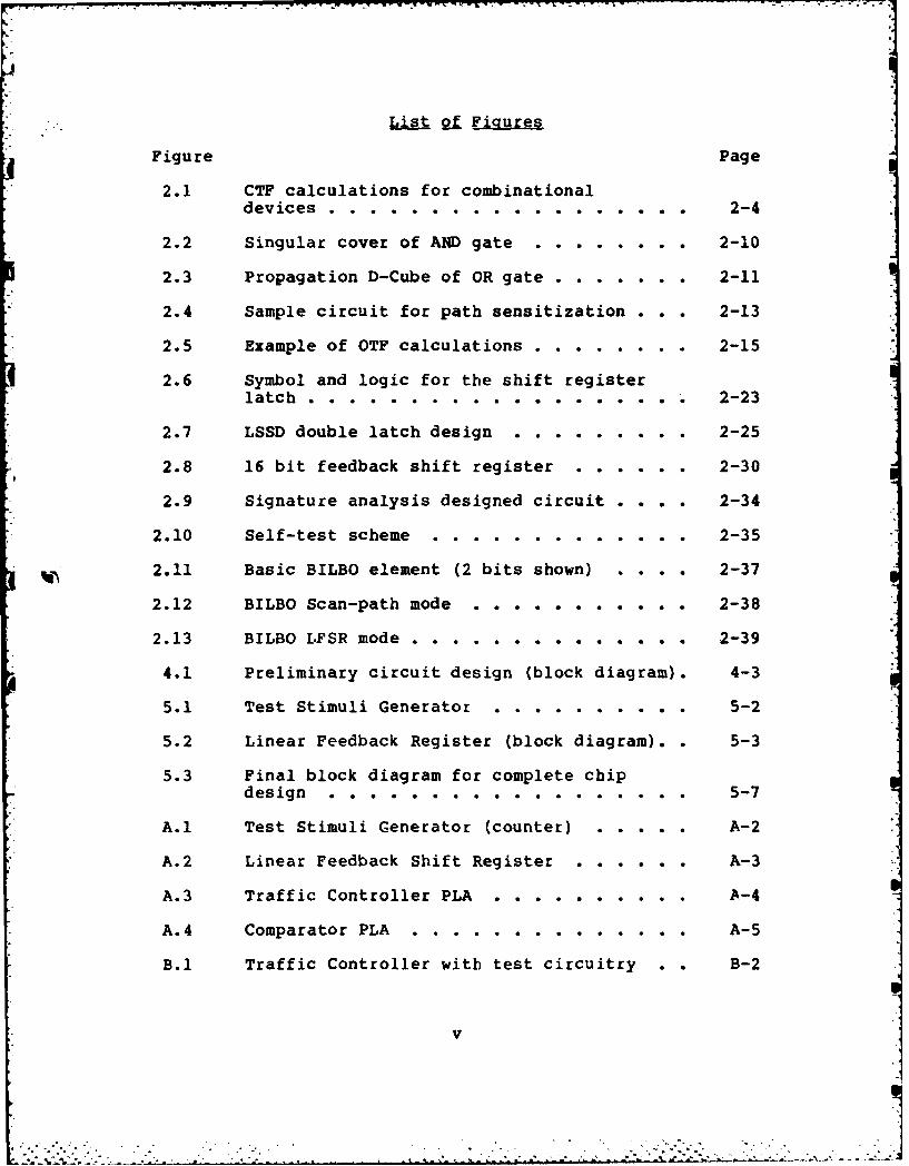
List of Figures
Figure Page
2.1 CTF calculations for combinationaldevices . . . . . . . . . . . . . . . . . 2-4
2.2 Singular cover of AND gate . . . . . ... 2-10
2.3 Propagation D-Cube of OR gate . . . . ... 2-11
2.4 Sample circuit for path sensitization . . . 2-13
2.5 Example of OTF calculations . ......... 2-15
2.6 Symbol and logic for the shift registerlatch . . . . . . . . . . . . . . . . . . . 2-23
2.7 LSSD double latch design . . . . . . . . . 2-25
2.8 16 bit feedback shift register . . . . . . 2-30
2.9 Signature analysis designed circuit . . . . 2-34
2.10 Self-test scheme . . . . . . . . . . . . . 2-35
2.11 Basic BILBO element (2 bits shown) . . . . 2-37
2.12 BILBO Scan-path mode . . . . . . . . . . . 2-38
2.13 BILBO LFSR mode . . . . . . . ....... 2-39
4.1 Preliminary circuit design (block diagram). 4-3
5.1 Test Stimuli Generator ... ......... . . 5-2
5.2 Linear Feedback Register (block diagram).. 5-3
5.3 Final block diagram for complete chipdesign . . . . . . . . . . . . . . . . . . 5-7
A.1 Test Stimuli Generator (counter) . . . . . A-2
A.2 Linear Feedback Shift Register . . . . . . A-3
A.3 Traffic Controller PLA . . . . . . . . . . -4
A.4 Comparator PLA . . . . . . . . . . . . . . A-5
B.1 Traffic Controller with test circuitry . . B-2
v
4
L. "istf Tables
Table Page
2.1 d-Intersection operator . . . . ......... 2-14
3.1 Transition table for light controller . . . 3-2
5.1 Test generation data for self-test . . . . 5-10
6.1 Effort to design circuit elements inChapter 5 . . . . . . . . . . . . . . . . . 6-4
6.2 Chip layout area used in Chapter 5design . . . . . . .......... . . 6-6
vi

Abstract
Very large scale integrated circuits are difficult to
test once fabricated. This is due to the large number of
internal circuit nodes that are not accessible as probe
points, and the small number of primary inputs and outputs
available to exercise and observe these internal nodes.
Methods to develop test vectors for such circuits (e.g.
d-Algorithm) are both difficult and time consuming. For
this reason a method is needed to design circuits which are
highly testable or self-testing.
Using computer aided design tools, a circuit is designed
which exhibits a self-test scheme. The design concepts used
include level-sensitive scan design and signature analysis.
When completed the circuit is evaluated from the standpoint
of how much design effort, circuit area used, and test
effort compares with the same parameters for a circuit
without testability characteristics included.
Environmental dependency (the conditions of circuit
operation) is an important consideration when determining if
self-test capability is warranted. When the circuit is one
which is inaccessible after deployment or needed without
much testing time available, self-test capability is
vii

worthwhile. This is a very necessary capability for
satellite systems or systems which must be replaced without
delay (e.g. component of F-16 fire control system).
For circuits which are strained for space on a
semiconductor chip due to their complexity, self-test
capability may not be practical due to the increased area
used for such circuitry. Finally, self-test capability
offers little help in determining the location of a fault if
the circuit malfunctions. Therefore, if deterministic fault
analysis is required, self-test capability will not provide
the necessary data.
IC
viii
-- - - - - - - *,-.--. - -- - -~
97
1. PROBLEM DEFINITION AND REVIEW OF LITERATURE
Background
How to test a system is a prime consideration when
designing a system. This is also true even when the system
under consideration is on a single semiconductor chip. As
technology advanced during the late 1960's, the number of
individual devices (transistors) on a single chip grew. In
the 1970's it was possible to put as many as one thousand
devices on a single chip. With this device density, the
problem of testing a system became harder to solve. As a
result, the ability to generate test patterns automatically
and conduct fault simulations with high fault coverage
declined (13:9).
In the late 1970's the state-of-the-art in chip design
increased from hundreds of devices on one chip to thousands
of devices on one chip. This technology is known as very
large scale integration (VLSI). With the emergence of VLSI
technology, it has become possible to put an entire
processing unit on a single chip. This system is known as a
microprocessor and is the heart of all modern day computers.
With literally hundreds of thousands of devices on such
systems, the testing problem has increased drastically.
1-1
0. . T . . . T .T T . . . - T i . . . . . .. . ... _ _ . .. . . . . .. ... .. . .. . .. . ... . . . . ... ... .

Testability refers to the ability to easily detect the
presence and location of as many faults within a system as
possible. It has become an important factor which affects
both the lifetime cost and the initial manufacturing cost of
a digital system .7:17). Because of these costs, some
manufacturers are foregoing rigorous testing approaches and
are accepting the risk of shipping defective products
(13:9).
Problem
Because of the increased use of VLSI circuits in the
(development of military systems, these circuits must be
readily available in the field. To be readily available
these circuits must also be highly testable. The present
problem is that these circuits are not easily tested by the
end, user once they are delivered. It is for this reason
that a method must be identified that will allow the design
of testable VLSI circuits. The goal of this study is to
identify a good method of designing testable VLSI circuits
which is easily implemented
VLSI systems are difficult to test for the following
three reasons: (1) The number of possible faults is
1-2
4
-

0I
extremely large. A VLSI circuit contains thousands of basic
components and interconnecting lines, all individually
subject to failure; (2) Access to internal components and
lines is severely limited by the small number of
input/output (I/O) connections available; and (3) Because of
the large number of possible faults which can occur,
adequate fault coverage will require a large number of test
patterns (7:17).
The purpose of this study is to investigate the current
methods of designing for testability and to design a circuit
which will exhibit the characteristics necessary to be
highly testable. The circuit to be designed will be complex
enough to show the advantages of self-test versus
traditional testing methods.
Two parameters which should be understood when
discussing testability are controllability and
observability. Controllability is the ease with which test
input patterns can be applied to the inputs of a subcircuit
by exercising the inputs of the primary system.
Observability is the ease at 4hich the outputs of a
subcircuit can be determined from the outputs of the primary
system (7:22). Controllability and observability can be
used to predict the difficulty of generating test patterns
for the primary circuit. This is discussed in detail in
Chapter 2.
1-3

_4
Self-testing refers to the ability of the circuit to
provide an error-detecting output as well as data output.
This error-detecting output contains information as to
whether or not the data is in error. This differs from
controllability and observability in that self-test requires
the addition of hardware and/or software to the chip
specifically for testing purposes.
Current Technology
There exist precise techniques for quantifying the
testability of a circuit. The previously mentioned concepts
of controllability and observability are measured by these
techniques.
Although these testability quantifying techniques exist,
measuring the testability of a circuit is only the first
step in solving the testability problem. Once a circuit is
known not to be highly testable, methods must be identified
which when incorporated into the design process increase
testability. The following is a summary of the more popular
methods for measuring testability.
Computer-Aided Measure for Logic Testability (CAMELOT)
(1:8-37) is an algorithmic testability analysis system. In
1-4

using this method, testability is quantified for each
circuit node. This is accomplished by determining the
controllability of each input node and then implementing a
process to transfer the controllability values across
devices in order to calculate values of other nodes. A
similar process is used to calculate observability values
for a circuit node (1:9). This has the effect of giving a
topological description of the circuit in terms of its
testability. Once this is accomplished, areas of poor
testability can be easily identified. This helps the test
generation engineers as well as the circuit designers.
A testability analysis algorithm for combinational VLSI
circuits known as VLSI Identification of Controllability
Testability, Observability, and Redundancy (VICTOR) is
currently being used. This algorithm identifies all
potential single redundancies and computes the
controllability and observability at every single-stuck
fault location in the circuit (11:397). This algorithm is
presently implemented in FORTRAN 77 and is undergoing
evaluation at the University of California, Berkeley, CA.
Controllability and Observability Measurement for
Testability (COMET) (2:364) is a testability analysis and
design modification software package developed at United
Technologies Microelectronics Center. This design package
1-5
Li -.-
has been implemented as part of a comprehensive computer
aided design system known as the Highland Design System.
COMET was developed as an extension of the SCOAP program
which was developed by L. Goldstein at Sandia National
Laboratories (2:365).
These methods, while adequate in performing their
intended function, do not improve a circuits testability.
Design methods must be identified to increase the
testability of a circuit. Several of these will now be
mentioned beginning with the most widely used method today,
the scan design technique.
Scan design techniques are techniques which allow a
synchronous circuit (a device with stored-state devices and
feedback) to be tested as a combinational circuit. In
stored-state devices, the next state of the device depends
on both the primary inputs and the current state of the
device. The dependency of the next state on the current
state is what causes the test generation problem. The test
programmer only has control over the primary inputs of a
traditionally designed circuit which means the state of the
device is neither directly controllable or observable
(1:48).
1-6
4 .I . . . . - . . - : . . I . . . . . .. . . L
-
To solve this problem a circuit must be designed which
will exhibit the following characteristics:
a. The stored-state devices can be tested
independently from the rest of the circuit.
b. The next-state of the device can be set to any
value desired.
c. The outputs of the combinational logic which
inputs the stored-state devices can be directly observable
(1:48).
By using a design method which accomplishes these
characteristics the circuit will be scan-path designed.
The most common implementation of scan-path design is
level-sensitive scan design (LSSD). To be considered
level-sensitive, a circuit state must be controlled by the
level of a control clock, not the clock edge transition.
Also, the steady-state response of the circuit must be
independent of the circuit propagation delays and the clock
rise and fall times (5:462-463).
By combining the level-sensitive and scan-path design
techniques, a sequential circuit can be designed which can
be tested without being dependent on a large number of
input, output, or intermediate probe points. This LSSD
circuit can now be tested using traditional test generation
techniques used for combinational circuits.
1-7
j]
Another design technique which can be used in concert Iwith LSSD is signature analysis. Signature analysis is a
process by which data is input into a circuit and then
clocked out through varying circuit nodes. As the
information passes through a node it is also input into a
shift register. The information in the register is then fed
back through a series of exclusive-OR gates in such a manner
that the resulting bit pattern in the register is the
signature of that node. Then if the signature of the node
is the same as the signature of a "correct" node from a
"good" circuit, the circuit passes the test. By combining
this process with LSSD, the nodes chosen may be nodes other
than primary inputs or primary outputs. This gives the
circuit self-test capability.
Another self-test technique is to use a circuit element
which can be made to operate as a shift register, a
scan-path element, or a Built-In Logic Block Observation
(BILBO) element (1:72-73). By using BILBOs as circuit
elements, the signature of a circuit node can be determined
without an external signature analysis circuit element. By
taking this technique one step further, the signature
produced by the BILBO element can be compared to the correct
signature on-chip. Therefore, the circuit correctness can
1-8

be determined entirely on-chip. This has the effect of
saving testing time and test designer effort (8:415).
Once the circuit has been designed, test generation
techniques can be used to develop a comprehensive test of
the circuit. One such method is used to develop tests for
scan designed circuits. This algorithm is known as Path
Oriented Decision Making (PODEM). Another algorithm
developed specifically for LSSD circuits is called Random
Path Sensitizing (RAPS) (1:83). These methods are mentioned
only to inform the reader that test generation techniques
exist specifically for LSSD circuits. Therefore, a test
engineer does not have to rely solely on test generation
techniques used for purely combinational logic.
Thesis Approach
This chapter has described the problems involved in
testing a VLSI device. In addition, it has discussed some
of the techniques currently available to determine circuit
parameters such as controllability, observability and
testabil.ty. Finally, some of the concepts of designing
testability into a circuit were discussed. They will be
examined in detail in Chapter 2.
1-9

Chapter 2 of this thesis will examine a specific method
of measuring the testability of a circuit. This is to give
the reader an idea of the difficulty involved in testing a
circuit by traditional means. Following this, Chapter 2
will examine some of the more popular design methods for
increasing the testability of a circuit as well as making a
circuit self-testing. Many of these techniques will be
incorporated in the design of Chapter 5.
Chapters 3, 4, and 5 show the requirements, system
design, and detailed design respectively for the self-test
system to be designed.
Finally, Chapter 6 discusses the evaluation of the
self-test technique and gives some guidelines as to when to
use it.
,
i-I
1-10

2. SUMMARY DISCUSSION OF DESIGN FOR TESTABILITY
This chapter will expand on some of the more important
concepts discussed in the previous chapter. From this
chapter, the reader should be able to grasp the effort
involved in designing a testable circuit. In addition, the
concepts described here will be applied to the design of a
sample circuit later in this thesis. The purpose of the
latter will be to illustrate these concepts.
Controllability and Observabilitv (1:8-37)
Before designing a testable circuit, one must be able to
quantify testability. As mentioned in the previous chapter,
the two ways of quantifying testability are controllability
and observability. Each of these concepts will now be
explained.
The first step in producing test patterns for a system
is to identify the subunits of the system. By breaking up a
circuit into smaller subsystems, the job of testing is made
much easier. The problem which follows however, is finding
a way to establish fixed values on the inputs of a
2-1
4!
subsystem. The inputs of a subsystem may be nodes internal
to the overall system and therefore are not primary inputs.
These nodes must then be initialized by assigning values to
the primary inputs. The ease at which a node is initialized
by assigning values to the primary inputs is defined as its
controllability (1:9).
Once the subsystem is initialized, its response must be
observed for correctness. Since only the systems primary
outputs are visible to the tester, the subsystem output
nodes response must be propagated through to them. The ease
at which this process is accomplished is known as
observability (1:9).
There are many ways of calculating controllability
4 values (CY) and observability values (OY). This section
will describe a method developed by R. G. Bennetts (1:8-37)
known as Computer-Aided Measure for Logic Testability
(CAMELOT).
Controllability.
In order to assign a CY to a circuit node, a range of
CYs must be established. Let a CY of 1 denote a node that
can be directly and easily controlled, and a CY of 0 denote
2-2

Ak
a node which cannot be controlled at all. Most CYs of
nodes, in reality, will fall somewhere between 0 and 1. A
primary node however, will always have a CY of 1 since it is
always directly controllable.
Consider a device with several inputs and outputs.
Assuming that the inputs were directly controllable (CY =
1), the CY of the output would be determined by the ease at
which the output could be set to a 0 or a 1. This is known
as the transfer function of the device. If the inputs of
the device are not directly controllable, the CY values of
the inputs must also be taken into account. Therefore, the
expression for controllability is shown in Eq (2.1).
N CY(output node) = CTF X f{CYs(input nodes)} (2.1)
CTF denotes the controllability transfer function of the
Idevice.
Controllability Transfer Function.
The CTF of an output is a measure of the ease at which a
4 1 can be generated at the output compared with the ease at
which a 0 can be generated at the output. The equation used
4
2-3
4'
to quantify the CTF is as shown in Eq (2.2) (1:10).
N(0) - N(l)CTF = I ----------- I (2.2)
I N(0) + N(1) I
In Eq (2.2), N(0) is the total number of ways a 0 can be
produced at the output and N(l) is the total number of ways
a 1 can be produced at the output (1:10). It can be seen
from this equation that if N(0) and N(1) are equal, then the
CTF will be equal to 1.
For purely combinational devices, N(0) and N(l) can be
determined from the device truth tables. Consider the
examples in Figure 2.1.
N(0) = 3N(l) = 1CTF = 0.75
N(0) =1N(l) f 3CTF = 0.25
*
Figure 2.1 CTF calculations for combinational devices.
2-4
Io" 4

For sequential circuits, those with stored-state
I devices, the calculation for CTF is different. The first
step is to create a truth table for the device under
consideration. Next, create a boolean expression for an
output. This expression must then be expanded so it is in a
sum of products form. Each term in this expression now
represents a collection of 1-entries.
Consider the equation of the output Q+ of a JK
flip-flop:
* Q+ = JQ'TPC + KQTPC + QT'PC + P' (2.3)
As long as all the product terms in this equation are
disjoint (no conjunctive term overlaps another) then N(l)
can be calculated.
To calculate N(l), first determine N(l) for each term.
Let the number of terms equal n. Also, let the number of
variables in a single term equal j. Then the N(l) of a term
is equal to 2(n-J).
Therefore, for each term, the results are as follows:
TERM U1
* JQ'TPC 2K'QTPC 2QT'PC 4PI 32
40
2-5
" S

The total number of N(l) entries are 40. However, some
of these entries would create an unstable output. These
invalid states must be discarded. The following
combinations of inputs produce invalid states:
INPUTS NUMBER OF INVALID STATES
P=0, C=I, Q=0 8P=l, C=0, Q=1 8P=0, C=0, 0=0 8
These 24 states must be subtracted from the original 40
N(l) states. This leaves 16 valid states, therefore N(l)
16.
To calculate N(0), start with the total number of
states, and then subtract the invalid states and the N(l)
states. In this case, N(0) = 64 - 24 - 16 = 16. This
yields a value of 0.8 for the CTF of Q+.
4
Qutput Controllability Values.
The next step is to compute the output CY values. As
stated previously, the CY(output node) = CTF X f{CYs(input
nodes)}. To calculate the function f, two situations must
be considered. One situation is when the circuit is
clocked, and one is when the circuit is unclocked. For the
2-6
unclocked mode, a simple arithmetic mean of the inputs is
used. For the clocked mode, the CY of each clock-controlled
input must be multiplied by the CY of the clock signal
before the mean is formed. Once these values are
calculated, the CY of the output can easily be found using
Eq (2.1).
Qbservabijity Values.
As with CY values, OY values range between 0 and i. An
OY value of 1 is assigned to a node which is completely
observable. This applies to a primary output. The OY then
decreases as a nodes observability decreases.
Again, as with CY values, OY values of internal circuit
nodes are dependent on the Observability Transfer Factor
(OTF). This factor is related to the ease at which a change
on an input can be propagated to an output (1:16).
When a test programmer wishes to propagate data through
a circuit, a propagation path must be identified from the
input to the output. In order to propagate the signal, the
path chosen must be sensitized. To sensitize the path,
certain node input values must be set which implies
controllability of those nodes. Therefore, the
2-7
observability of a node is directly related to the CY values
(of the related input values. The relation between these
factors is shown in Eq (2.4).
OY(at output) = OTF X OY(at input) X
g(CYs on supporting inputs) (2.4)
Observability Transfer Factor.
First, the OTF must be determined. The OTF from an
input I to an output 0 is denoted OTF(I-0). This value will
range between 0 and 1. An OTF of 0 denotes that there is no
way of propagating data from input to output. An OTF of 1
indicates that the data is always propagated from input to
output.
The exact calculation of a node OTF involves the use of
concepts of the d-Algorithm. The two factors involved are
propagating d-Cubes (PDCs) and non-propagating d-Cubes
(NPDCs). Each PDC identifies the input to be sensitized,
the supporting input values which will support the path, and
the sensitized path output. Each NPDC identifies the
sensitized path input, the supporting input values which
block the path, and the insensitive output. The manner in
2-8
I

**1
which the values are determined is shown in the following
paragraphs.
The basic premise of the d-Algorithm is to sensitize all
possible paths from the site of a possible fault to all
circuit outputs simultaneously. This differs from the path
sensitization method in that the d-Algorithm generates all
possible paths and it also does this in a methodological
manner.
There are three major steps involved in implementing the
d-Algorithm. They are as follows:
1. Determine which gate in the circuit will be tested.
This gate will be tested in terms of its inputs and output.
2. Generate all possible paths from the gate under test
to all outputs simultaneously. When each path is
considered, check if reconvergent fanout has occurred,
making the path useless. If so, cancel this path. This
step is known as the d-drive.
3. Construct an input vector which will excite all the
paths generated during the d-drive. This is an algorithmic
process that duplicates the effort involved in the backward
trace phase of the path sensitization method.
There are three entities or conditions that must be
understood before an implementation of the d-Algorithm can
be used for CY and OY analysis. These are: (1) singular
2-9
cover; (2) the propagation d-Cube; and (3) the primitive
d-Cube of a failure. Each of these will now be discussed.
The singular cover of a logic gate is a compacted truth
table for that gate (4:30). Consider the gate and its
singular cover in Figure 2.2.
1 2
C1 = 1 1 13 C2 = x 0 0
C3 = 0 x 02
x f don't care
Figure 2.2 Singular cover of AND gate.
Each row in the truth table is called a cube, and each
cube establishes a relation between the inputs and the
output of the gate. Cube Cl of Figure 1 states that if
input 1 and input 2 have logic l's on them, then output 3
will be a logic 1. Cube C2 states that output 3 will be a
logic 0 if input 2 is a logic 0, regardless of the value of
input 1.
In addition, the singular cover of a combinational
circuit is comprised of the singular covers of the gates
which comprise it.
The propagation d-Cube (6:24-26) is the notation of a
cube which forces an input to be the sole determining factor
in the value of the output of a gate. The symbol "d" is
2-10
S.
I.
used as the variable. It can take on the value of either a
logical 1 or 0, however, all d's in a cube must take the
same value.
An example can be seen in Figure 2.3
1 1 2d 0 d
3 0 d d
2
Figure 2.3 Propagation D-Cube of OR gate.
The first cube of Figure 2.3 can be expanded as follows:
1 2 31 0 1
0 0 0
It states that output 3 will equal input 1 as long as input
2 is a logical 0.
For simple cases, the propagation d-Cubes can be written
down by inspection, however for more complex cases, an
algorithm is needed.
The algorithm is implemented by intersecting the cubes
of the gate's singular cover. Only those cubes with
2-11

different output values are intersected, and the cubes are
intersected using the following rules:
(*0 00 denotes the statement w0 intersecting 00)(0 0) = (0 A x) = (x 0 0) = 0(1 Ali) = (1 A x) = (x 1) = 1(x x) = x(1 0 0) =d(0 1) =d'
Therefore, for the gate in Figure 2.2, the propagation
d-Cubes are as follows:
1 2C1 C2 = 1 d dCl C3 = d 1 d
The primitive d-Cube of a failure (6:21-24) is used to
show a test for a failure in terms of the inputs and output
f the failed gate. Primitive d-Cubes of a failure are
constructed just as was done for the propagation d-Cubes.
However, here the cubes to be intersected are chosen
differently. One cube is chosen from the failure free
gate. The other cube is the corresponding cube (input-wise)
from the failed gate. The inputs are intersected as before.
The outputs are intersected by the following convention.
If the output is a logical 0 in the failure free gate,
and the output of the failed gate is a logical 1, then the
output of the intersection of these cubes is a d'. If the
2-12
values are reversed, the output of the intersection is a d.
When combining two or more gates in succession, we wish
to generate a sensitized path from the input of the first
gate to the output of the second (4:33). Consider the
circuit in Figure 2.4.
3
Figure 2.4 Sample circuit for path sensitization (4:33).
The propagation cubes we wish to intersect to generate a
path from signal 1 to signal 5 are: (1) Cl = dlxdx; and (2)
C2 = xxOdd. These cubes are intersected using the following
rules:
d @ x =d
1@ x=1
x@O=O
d@d=d
x @d=d4
2-13
• ,- .. - : . . •I ", - t- -. :' '. "fl "- .. L.. ii]"
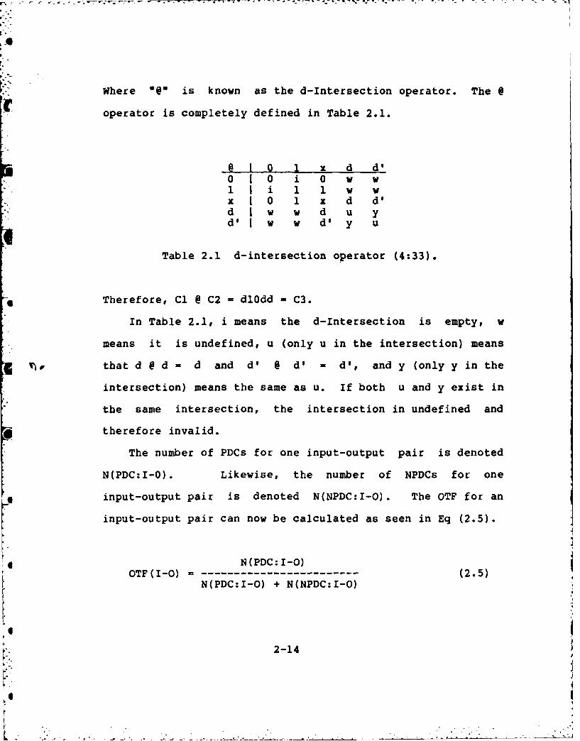
Where @ is known as the d-Intersection operator. The @
operator is completely defined in Table 2.1.
@ 0 1 x d d'0 0 i 0 w wlii 1 1 w wx 0 1 x d d'd w w d u yd' w w d' y U
Table 2.1 d-intersection operator (4:33).
* Therefore, C1 @ C2 = dlOdd - C3.
In Table 2.1, i means the d-Intersection is empty, w
means it is undefined, u (only u in the intersection) means
that d @ d = d and d' @ d' = d', and y (only y in the
intersection) means the same as u. If both u and y exist in
the same intersection, the intersection in undefined and
therefore invalid.
The number of PDCs for one input-output pair is denoted
N(PDC:I-0). Likewise, the number of NPDCs for one
input-output pair is denoted N(NPDC:I-O). The OTF for an
input-output pair can now be calculated as seen in Eq (2.5).
OTF(I-O) ------ N(PDC: - (2.5)
N(PDC:I-O) + N(NPDC:I-O)
2-14
it °- ir
r~~~~ ~ ~ ~ -- .- --- , - , -. -' - . c .. .. . I . ,---- -- .. ,-,...... . C
L.L
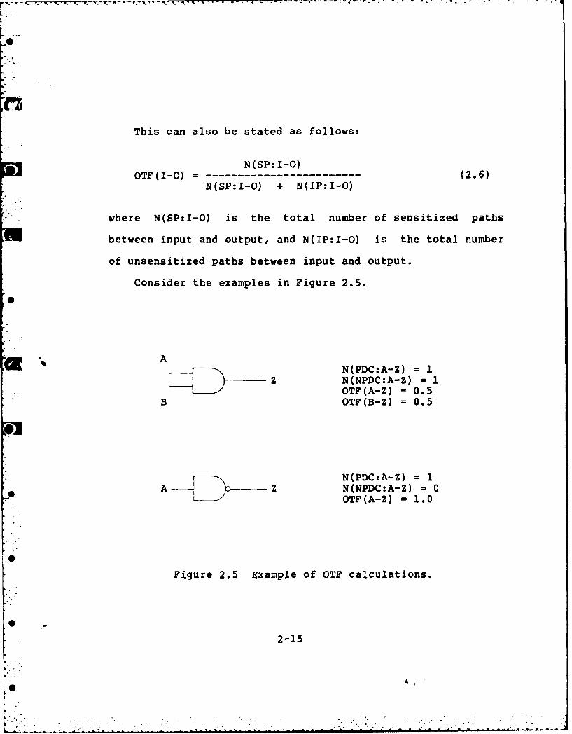
This can also be stated as follows:
N(SP: 1-0)OTF(I-O) ------------------------ (2.6)
N(SP:I-0) + N(IP:I-0)
where N(SP:I-0) is the total number of sensitized paths
between input and output, and N(IP:I-0) is the total number
of unsensitized paths between input and output.
Consider the examples in Figure 2.5.
N(PDC:A-Z) =1
Z N(NPDC:A-Z) =1
OTF(A-Z) = 0.5B OTF(B-Z) = 0.5
0(D:-Z
A Z N(PDC:A-Z) = 1
OTF(A-Z) =1.0
Figure 2.5 Example of OTF calculations.
2-15
to0--- --

For stored-state devices, calculating the OTF is more
difficult. It can be done as follows:
a. identify all possible combinations of inputs.
b. delete those which create unstable states.
c. decide which combinations of inputs result in
the propagation of a fault. This must be done for each
input for every valid state.
d. the number of combinations of inputs which
result in the propagation of a fault for any one input, is
the number of sensitized paths of that input. All other
paths for that input are non-sensitized paths.
e. the OTF for each I-0 pair can now be calculated
using Eq (2.6).
Input Observability Values.
Now that the OTF is calculated, a method is needed to
calculate the input OY values. To accomplish this, the
multiplicative property of OY values must be stated. It is
as follows:
OY(A-C) = OY(A-A) X OY(A-B) X OY(B-C)
The next step is to calculate OY(A-B) and OY(B-C).
OY(A-B) = OY(A-A) X (difficulty in transfering a value from
2-16
6!

I.
A to B). The difficulty factor can be further broken down
to equal OTF X (the average CYs of the supporting inputs).
Since the CYs and OTF have already been calculated, the OY
of the node under test is a straightforward exercise. There
are several methods that can be used to determine the OYs of
circuit nodes. The method which takes the least time is to
calculate the OY at each primary output and then work back
toward the inputs. This method requires only one pass
through the circuit for each primary output.
A special case to be considered is path reconvergence
(1:23). If a circuit has path reconvergence of unequal
length, OY values are calculated for the shortest path and
the other paths should be blocked. For path reconvergence
of equal length, the OY value is calculated for both paths
and the higher value is used. The other path should then be
blocked.
Testability Values.
At this point, both the controllability values and
observability values have been calculated. The next step is
to use these values to calculate a value for the testability
of each circuit node, and then for the entire circuit. The
2-17

equation for testability of each node (TY(node)) is as
follows:
TY(node) = CY(node) X OY(node) (2.7)
This ensures that the value of TY will also fall between 0
and 1.
Once the TY nodal values are calculated, a figure of
testability merit is given to the entire circuit as follows:
(sum of nodal TYs)TY(circuit) = (2.8)
number of nodes
The method described above for determining CY, OY, and
TY values are the principles behind CAMELOT. As stated
previously, this is only one way of quantifying these three
circuit characteristics.
Once the CAMELOT process is complete, the results are
very helpful to the design and test engineers. If the
engineers know a circuit has a section that is not very
testable, a decision can be made as to the relative gains of
redesigning the circuit to make it more testable. The
CAMELOT results will also have an impact on the future
circuit designs as well.
2-18

Scan-Path Design
After describing several methods to measure a circuits
testability, other methods are needed to design a testable
circuit. Scan-path design fills this need. This section
will briefly describe the principle behind scan-path design.
A more thorough description will be given in the next
section. That section will discuss the most popular
implementation of scan design, LSSD.
The basic principle behind scan design is to provide the
ability to test the stored-state circuit elements apart from
the rest of the circuit (1:48). This is accomplished by
inserting a multiplexer immediately before each stored-state
device. The multiplexers are controlled by a single SCAN
SELECT signal. When the signal is low, the stored-state
devices are connected to the combinational circuitry as
would be done in a non-scan-path designed circuit. When the
signal is high, the stored-state devices are reconfigured
into a single, serial shift register (1:48-49).
The purpose of scan-path design is threefold:
a. As stated previously, to allow the stored-state
devices to be tested separately from the combinational
elements in a circuit.
b. To allow the tester to preset the present or
2-19
I

next state of the sequential circuit under test.
C. To allow the tester to directly observe the
outputs of the combinational circuitry which input the
stored-state devices (1:48).
The following events can now be accomplished:
a. Reconfigure the stored-state devices to a
serial shift register.
b. Shift in a specified state to start the test.
c. Reconfigure the circuit to its normal mode of
* operation.
d. Clock the circuit a specified number of times.
e. Again reconfigure to the shift register mode
'. (scan-path mode).
f. Shift out the combinational circuits outputs.
Because of the limited number of primary inputs and
outputs inherent in VLSI devices, scan-path design is an
ideal way to directly enhance controllability and
observability in these type of circuits.
A more detailed discussion of scan-path design follows
as well as a discussion of LSSD.
0
2-20

Scan-Path Design and LSSD
C1'There are two independent principles behind
level-sensitive scan design. They are level-sensitive
design, and scan-path design. Each of these principles will
now be discussed.
A logic subsystem is considered to be level-sensitive if
the steady state response to any allowed input state change
is independent of the circuit and wire delays within the
subsystem. Also, if the input state change involves more
than one input signal change, the order in which they are
changed does not effect the steady state response of the
output (5:462-463).
By designing a system using the above criteria, the
circuits dependency on ac parameters such as rise and fall
time, and propagation delays is reduced (1:53).
* Scan-path design refers to the ability to transform all
internal storage elements in such a way as to operate them
as shift registers. This has the effect of transforming a
sequential circuit into a combinational circuit. By doing
this, test generation techniques for combinational circuits,
such as the d-Algorithm, can be applied. This greatly
reduces the complexity of test generation for the circuit
under test.
-
2-21

To accomplish the first design objective,
level-sensitivity, the basic storage element should be one
which does not contain a hazard or race condition. To
satisfy this restraint, the polarity hold latch was chosen
as the basic storage element. This latch has two input
signals and one output signal. The input signals are a
clock signal C, and a data input signal D. The output is a
data output signal L.
When C = 0, the latch cannot change state. When C = l,
the state of the latch is determined by the value of D. The
value of D should only change when C = 0. Then when C = 1,
the state of the latch will change. C should not change to
1 before the value of D has had a chance to stabilize. This
causes the latch output L, to be set to the new value of D
when the clock signal C occurs. The clock signal must
remain high for some value T, where T is the time required
for the signal to propagate through the latch. By latching
in this manner, the change in latch value is not dependent
on the rise or fall time of the clock signal (5:463).
By causing the polarity hold latch to operate as a shift
register, the second design objective, scan-path design, can
be achieved.
To create a shift register latch (SRL) with polarity 7
hold latches, the configuration in Figure 2.6 is
implemented.
2-22
>A
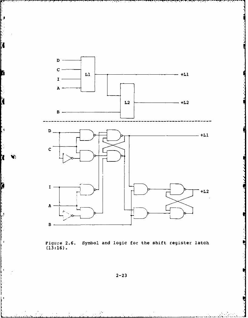
D
CLi +LI
A-
4L2 +L2
B
D+L1
C
* +L2
A
B
Figure 2.6. Symbol and logic for the shift register latch(13:16).
2-23

To operate this circuit as part of a scan path, clock
Isignal A is set to a 1. This allows scan data input I to be
latched into Ll. Then, as clock signal A is set to 0, clock
signal B is set to 1. This transfers the value in Ll to L2.
As clock signal B returns to 0, the value in L2 is
permanently latched (1:54).
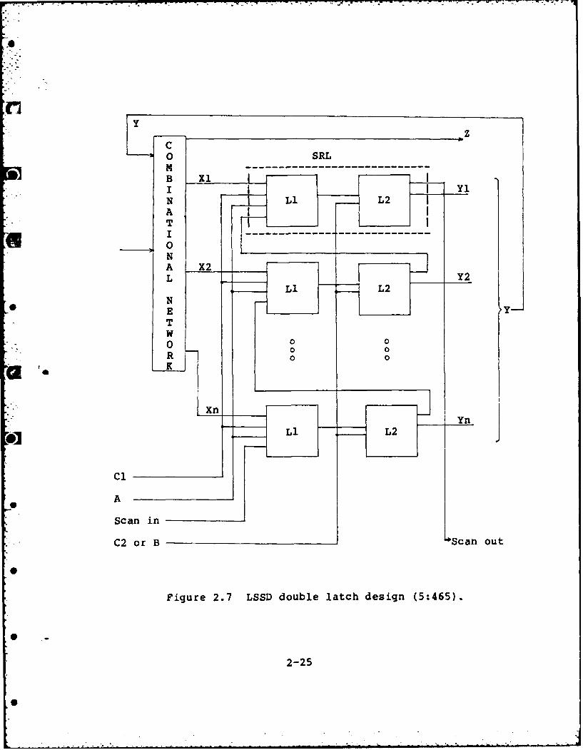
Once the SRL is designed, several SRLs are connected to
form a scan-path shift register. This is accomplished by
connecting the L2 output of one SRL to the scan data input I
of the following SRL. This continues until all the SRLs are
connected. Clock signals A and B are common to all the SRLs
(1:54). A particular configuration of an LSSD circuit known
as a double latch (Double latch indicates that Ll and L2 are
in the system data path. There are other designs such as
the single latch where Ll is the system output and L2 is the
scan path output.) is shown in Figure 2.7
I
~2-24
y
0 SRL
I Y
ATI --- - - - - - - - - - - -
0NA X2L Y2
Li L2N
S EYTw0 0 0
0 0R 0 0at K
Cl1
A
Scan in
C2 or B Sa u
Figure 2.7 LSSD double latch design (5:465).
2-25

DesiQn Rules for LSSD.
The following design rules, when adhered to, will result
in a circuit which has the characteristics of LSSD. If a
circuit meets rules 1-4, it is said to be level-sensitive.
If it meets rules 5 and 6, it is scan-path designed.
1. All internal storage elements must be implemented in
polarity-hold latches.
2. The latches must be controlled by two or more
non-overlapping clocks such that latch X may feed the data
port of latch Y, if and only if, the clock that sets the
data into latch Y does not clock latch X.
3. All clock inputs can be set low independent of one
another and any one clock can be set high independent of the
other clock inputs.
4. Clock primary inputs cannot feed SRL data inputs
either directly or indirectly. They may feed only clock
inputs.
5. All system latches are implemented as part of an
SRL. All SRLs must be interconnected into one or more shift
registers each having one scan-in input, one scan-out
output, and scan control clocks.
6. There must exist some primary condition,
controllable from the primary inputs, known as the
2-26
V .. . .___i

Oscan-state* such that:
a. All SRLs are connected as a scan path.
b. All SRL clocks, except the shift clocks A and
B, can be held inactive.
c. All shift clocks are controlled by the
corresponding primary input clock.
The major advantages and disadvantages of LSSD will now
be discussed.
Advantages of LSSD.
The advantages of LSSD are the following:
1. Because the operation of the system under test is
independent of the ac characteristics of the circuit, many
tests will be eliminated which test for such things (5:466).
2. For scan designed circuits, test generation is
required for only combinational logic. This task is not as
difficult as designing tests for sequential circuits.
Algorithmic procedures can be used for test generation
(1:61).
3. The state of every latch in the system can be
examined during any one clock pulse without disturbing the
state of the system. This is assuming that all the data is
2-27
• .I"o . , . -.. • -

shifted back into the latches in the same order it was
shifted out (5:466-467).
Disadvantages of LSSD.
The major disadvantages of LSSD are the following:
1. The system package will require four additional I/O
pins for the signals I, A, B, and Y.
2. Polarity-hold latches are two to three times more
complex than simple latches. This has the effect of
increasing real-estate usage by approximately 20%, and
lowering reliability (5:467).
3. External asynchronous input signals must not change
more than once every clock cycle. This is because a full
clock cycle is needed to latch the input data (5:467).
*4. The scan design implementation places constraints on
the design of a logic circuit. Many stored-state devices
currently in use will not be acceptable because they do not
L4 meet the LSSD criteria (1:61).
Level-sensitive scan design is a design method which
alleviates some of the problems associated with testing a
completed circuit. Test generation techniques associated
with combinational logic can be used with sequential logic
2-28
• . . . + . . .. .4- . . - . . ,. ,, + ,. " " . . + . - .+ . . + , ..

if the system was designed using LSSD.
Additional testing schemes such as signature analysis,
which will be discussed next, can be used in concert with
LSSD to further enhance the circuits testability. This is
especially useful when the circuit under test has few probe
points.
With the problem of controllability and observability
inherent in any VLSI circuit, LSSD provides a valuable
alternative to traditional design and testing methodologies.
Siqnature Analysis
A circuit which has been designed using the principles
of LSSD is said to be testable. However, a method is
available which would allow an LSSD circuit to be even more
testable. In fact, a circuit could be designed in such a
manner as to allow self-test capability.
Before discussing self-test further it is necessary to
describe signature analysis in detail. This is because
signature analysis combined with LSSD comprise the self-test
design strategy.
2-29
4 ...
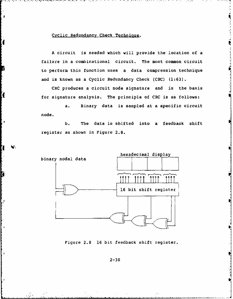
Cyclic Redundancy Check Technique.
A circuit is needed which will provide the location of a
failure in a combinational circuit. The most common circuit
to perform this function uses a data compression technique
and is known as a Cyclic Redundancy Check (CRC) (1:63).
CRC produces a circuit node signature and is the basis
for signature analysis. The principle of CRC is as follows:
a. Binary data is sampled at a specific circuit
node.
b. The data is shifted into a feedback shift
register as shown in Figure 2.8.
hexadecimal displaybinary nodal data
16 bit shift register
Figure 2.8 16 bit feedback shift register.
2-30
]I

The initial contents of the register is set to all Os.
c. After a predetermined number of clocked shifts
into the register, the hexadecimal value of the register is
displayed.
d. The hexadecimal value is compared against a
predetermined "correct signatureu for that node.
Because of the register feedback path, any corruption of
the nodal binary data will result in a incorrect hexadecimal
display for that node. There is a possibility that a faulty
bit stream will result in a correct nodal signature.
However, the probability of this occurring is 1 in 2n
(1:63) where n is the number of bits in the shift register.
This is extremely small and therefore is neglected.
4 A The bit stream which is shifted into the device under
test should ideally be one that will exercise all possible
faults for the circuit. Methods can be used (such as the
d-Algorithm) to develop bit streams for the required fault
coverage.
In order to find the location of a possible fault, the
nodal signature of a primary input is compared to a correct
signature for that node. If it is the same, the next node
in the circuit is checked. Each node toward the primary
outputs, in turn, is then checked until an incorrect
signature is found. In this way, the location of a fault
can be determined.
2-31

Now that a method of determining a nodal signature has
been identified, it is desirable to implement the circuit in
such a manner as to have the test stimuli generated on the
same chip as the device under test. This is known as the
signature analysis technique.
Signature Analysis Technique.
There are two features which must be added to a circuit
in order for it to be designed to signature analysis
standards. As stated earlier, it must have an on-board test
stimuli generator. Secondly, it must have the ability to
break its global feedback paths (1:68). The on board test
stimuli generator can take one of two forms. It can be
implemented as read only memory (ROM). This type of circuit
generates algorithm produced type data (e.g. d-Algorithm).
The other form of test generator produces pseudo-random test
stimuli. This type of generator could be implemented as a
counter.
Although deterministic test stimuli sensitize every path
from the inputs to the outputs, pseudo-random test stimuli
may be sufficient. A rule of thumb which may be used is
known as the node excitation requirement (1:69). This
2-32
'1

requirement states that every circuit node changes value at
least once due to the test stimuli placed on the primary
inputs.
Global feedback paths must be broken for the following
reason: A failure in one node (assuming the node is in the
feedback path) will cause the failure to be observed at many
other nodes. This makes it very difficult to determine the
location of the original fault (3:133).
A typical signature analysis approach is shown in Figure
2.9.
2-33
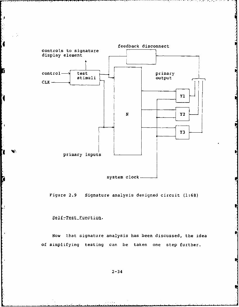
feedback disconnectcontrols to signaturedisplay element
control--- test ,primarystimuli - output
CLK-
primary inputs
system clock
Figure 2.9 Signature analysis designed circuit (1:68)
591f-Test Function.
Now that signature analysis has been discussed, the idea
of simplifying testing can be taken one step further.
2-34
*. .-~ . .* * - - . . *. .....
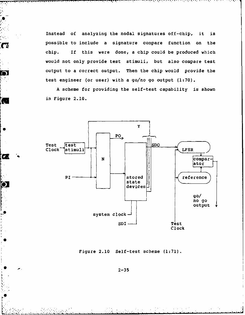
Instead of analyzing the nodal signatures off-chip, it is
possible to include a signature compare function on the
chip. If this were done, a chip could be produced which
would not only provide test stimuli, but also compare test
output to a correct output. Then the chip would provide the
test engineer (or user) with a go/no go output (1:70).
A scheme for providing the self-test capability is shown
in Figure 2.10.
*Y
T e st test- SDOClock stimuli - LFSR
0&
N ccompar-, , tator
PI stored referencestatedevicesJ
go/. f lno go
system clockTotu
SDI TestClock
Figure 2.10 Self-test scheme (1:71).
- "2-35
t*- . .." • '

The scan out data is clocked into a linear feedback
shift register (LFSR). This produces the signature of the
circuit in the test mode. This signature is then compared
to a bit stream located in the reference register. If the
signatures match, the go/no go line is set high. Otherwise,
it is set low.
By using this method, the test is transparent to the
user. Only the go/no go signal is observed. A disadvantage
of this simplicity however, is that if the signal indicates
a no go condition, it is difficult to discover the location
of the fault.
Built-In Logic Block Observation (BILBO)
In order to make self-testing circuitry easier to
design, it is desirable to use a register that can be used
for both data transfer and fault detection purposes. This
device is known as a BILBO element (9:40).
Each BILBO element is composed of a flip-flop register
row with additional gates for shift and feedback operations.
A BILBO element is shown in Figure 2.11.
2-36
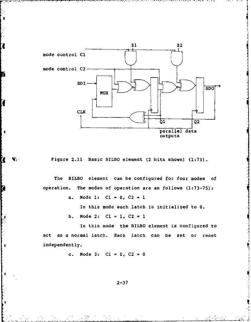
I
Zi 22
mode control Cl
mode control C2
SDISDO
parallel dataoutputs
Figure 2.11 Basic BILBO element (2 bits shown) (1:73).
The BILBO element can be configured for four modes of
operation. The modes of operation are as follows (1:73-75):
a. Mode 1: Cl = 0, C2 = 1
In this mode each latch is initialized to 0.
b. Mode 2: C1 = 1, C2 = 1
In this mode the BILBO element is configured to
act as a normal latch. Each latch can be set or reset
independently.
c. Mode 3: Cl = 0, C2 = 0
2-37
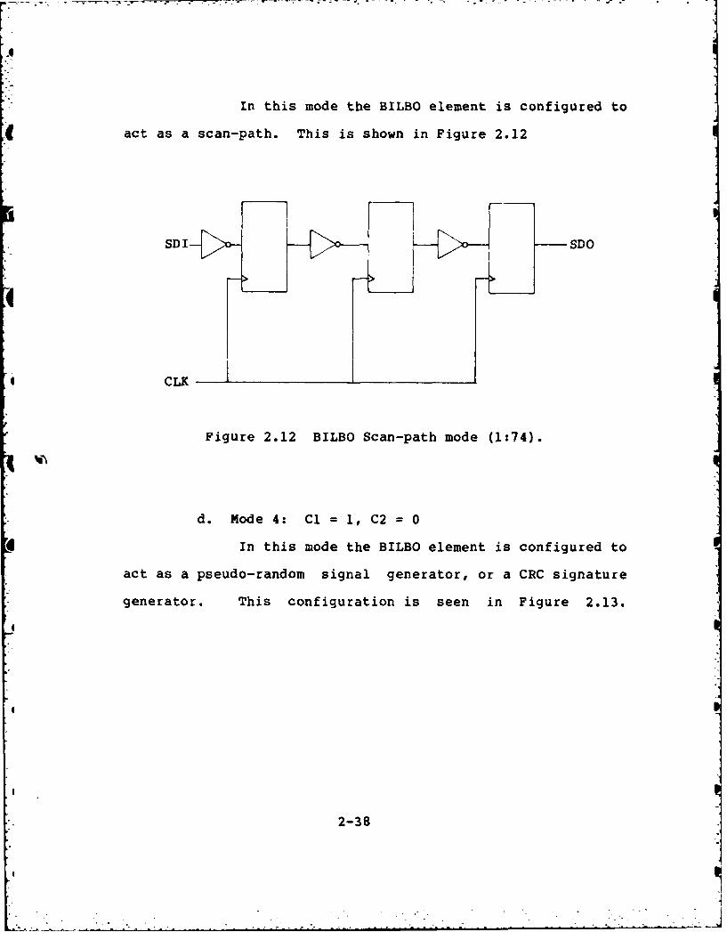
In this mode the BILBO element is configured to
act as a scan-path. This is shown in Figure 2.12
SDI-[>-SDO
4/
CLK
Figure 2.12 BILBO Scan-path mode (1:74).
d. Mode 4: Cl = 1, C2 = 0
In this mode the BILBO element is configured to
act as a pseudo-random signal generator, or a CRC signature
generator. This configuration is seen in Figure 2.13.
2-38
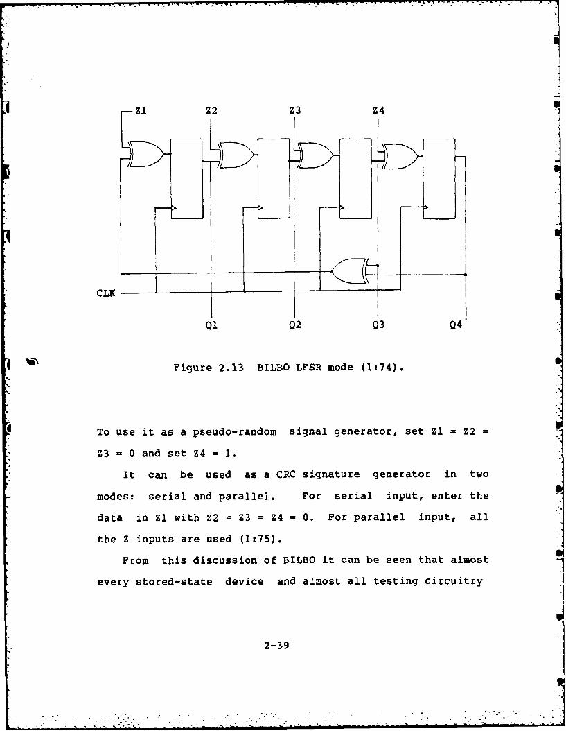
Zi Z2 Z3 Z4
CLK_ _ _ __ ___-
QI Q2 Q3 Q4
Figure 2.13 BILBO LFSR mode (1:74).
To use it as a pseudo-random signal generator, set Zi = Z2 =
Z3 = 0 and set Z4 = 1.
It can be used as a CRC signature generator in two
modes: serial and parallel. For serial input, enter the
data in Zl with Z2 Z3 = Z4 = 0. For parallel input, all
the Z inputs are used (1:75).
From this discussion of BILBO it can be seen that almost
every stored-state device and almost all testing circuitry
2-39

can be implemented using a BILBO element. With the help of
BILBO, the advantages of a high speed built-in test and the
high fault resolution of scan-path techniques, VLSI testing
can be made much more simple, efficient, and accurate
(9:41).
2'42-40
6 -:
3. STATEMENT OF REQUIREMENTS AND JUSTIFICATION
The purpose of this chapter is to indicate the
requirements for the VLSI integrated circuit to be designed
in the subsequent chapters. Before enumerating the specific
requirements, the general purpose of the circuit will be
discussed.
The purpose of this thesis is to demonstrate the value
of design for testability. A chip will be designed to
incorporate many of the concepts of design for testability,
yet the primary function of the circuit will be fairly
simple. The purpose of this is to show the self-test
capability without becoming engrossed in the complexity of a
complex circuit function.
The remaining portions of this chapter will describe and
justify the functional, performance, and implementation
requirements for the chip to be designed.
Functional Reouirements
The following are the functional requirements along with
their justification:
3-1
. m. .. .. .. : . . .". . ..- . -I
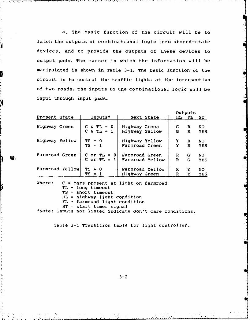
a. The basic function of the circuit will be to
latch the outputs of combinational logic into stored-state
devices, and to provide the outputs of these devices to
output pads. The manner in which the information will be
manipulated is shown in Table 3-1. The basic function of the
circuit is to control the traffic lights at the intersection
of two roads. The inputs to the combinational logic will be
input through input pads.
OutputsPresent State Inputs* Next State HL FL ST
Highway Green C & TL = 0 Highway Green G R NOC & TL = 1 Highway Yellow G R YES
Highway Yellow TS = 0 Highway Yellow Y R NOTS = 1 Farmroad Green Y R YES
Farmroad Green C or TL = 0 Farmroad Green R G NOC or TL = I Farmroad Yellow R G YES
Farmroad Yellow TS = 0 Farmroad Yellow R Y NOI TS = 1 Highway Green R Y YES
Where: C = cars present at light on farmroadA TL = long timeout
TS = short timeoutHL = highway light conditionFL = farmroad light conditionST = start timer signal
*Note: Inputs not listed indicate don't care conditions.
Table 3-1 Transition table for light controller.
3-2

b. The circuit will include stored-state devices
as well as combinational circuitry. The purpose of this is
to show how scan-path design will simplify the testing of
circuits which use stored-state devices.
c. The circuit will include a linear feedback
shift register to be used to produce a signature of the scan
data output. The purpose of this is to have a means of
observing the output of the scan-path, compressing the data,
and comparing it to a known correct signature.
d. The test stimuli will be provided by an on-chip
test stimuli generator. The purpose of this is to create a
chip with self-test capability.
e. The output signature will be compared against a
predetermined "correct" signature on-chip. This will enable
a go/no go decision to be made on the chip. Therefore, one
of the test outputs will be a go/no go signal. The other
test outputs will consist of signals at pre-selected probepoints of the operational and testing circuitry. These
probe points would not ordinarily be available to the user,
but will be examined for the purposes of this thesis.
f. Since the objective of this design is to
illustrate the concepts of design for testability, and not
test generation, the combinational circuitry will not be
3-3

complex. Therefore, in lieu of pure combinational logic, a
programmable logic array (PLA) will be used.
g. The outputs of the PLA will be included in the
scan-path. The purpose of this is to further expand the
comprehensiveness of the test.
h. A two-phase, non-overlapping clocking scheme
will be used.
Performance Reauirements
The following are the performance requirements along
with their justification:
a. The linear feedback shift register will be at
least six bits long thereby making the probability of a
corrupt bit stream producing a correct signature only 1 in
128.
b. Since level-sensitive scan design does not
depend on rise and fall times of clock transitions, no
performance requirements are needed pertaining to the timing
of the changing circuit signals.
c. The testing scheme for the combinational
circuitry does not necessarily have to provide 100% fault
coverage. Instead of a deterministic testing approach, a
4

jI
pseudo-random approach may be used. Again, this is due to
the fact that the purpose of this design is to produce a
testable circuit, not to develop a set of test vectors using
and algorithmic approach.
d. The controllability and observability values
for each node of the scan path should be the same as the
values for the primary inputs and outputs respectively.
Ideally, this value will be 1.
e. The PLA shall be of sufficient complexity as to
include at least six inputs and five outputs.
f. The chip to be designed will be either a 40,
64, or 128 pin package. This will depend on the number of
test outputs which are used.
Implementation Requirements
The following are the implementation requirements and
their justification:
a. NMOS technology will be used.
b. The following CAD tools will be used:
cll
cifplot
Mextra
3-51
Plagen
Mkpla
Es im
clldrc
RNL
c. All CAD work will be accomplished on a Digital
VAX 11/780 running the UNIX operating system. These are the
resources available at AFIT.
d. The chip to be designed will be scaled to 2.5
micrometers/lambda. This is the current fabrication
technology.
3-
3-6

4. SYSTEM DESIGN
This chapter contains the preliminary design of the
project circuit along with rational as to the basis of the
design. Also included is a test plan and scenario, and an
operational plan and scenario.
Project Statement
The purpose of this project is to produce a VLSI circuit
which exhibits the property of being testable. Testability
of the circuit will be measured according to the criteria
described in earlier chapters. More specifically, the
circuit will contain all the features described in Chapter
3.
The function of the circuit is very simple. It merely 0
accepts an input, manipulates the input data in a predefined
manner (as shown in Table 3-1) through a PLA, and stores the
result. The result can then be observed on data output
nodes. The simplicity of this circuit, as stated earlier,
is to demonstrate the testable characteristics more easily.
4-1
-- - - - - - -- -t

Preliminary Circuit Design
The preliminary circuit design is shown in Figure 4.1.
This block diagram shows the circuit design at the register
transfer language level.
Each of the major circuit elements will now be
discussed:
a. Test stimuli generator - this circuit element
will be implemented as a counter. This is to ensure that
all possible input combinations will be realized, and thus
provide an acceptable test set.
b. Combinational logic - this circuit implements
the logic transition design in Table 3-1 and will be
4 ~designed as a PLA. This is the only internal circuit
element which is needed to perform the primary circuit
function. Everything else is testing circuitry. The PLA
outputs will be designed with LSSD characteristics making
the circuits overall testability even greater.
c. Stored-state devices - these circuit elements
will be implemented using LSSD shift-register latches.
d. Reference register - a simple serial-in,
parallel-out register will be used.
e. Linear feedback shift register (LFSR) - a 0
cyclic redundancy check circuit element will be implemented
4-2
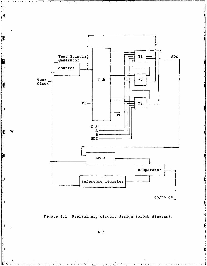
Y
Test Stimuli YSDOGenerator Fcounter
Test PLACloc-,
PI--3
POIL
CLK
BSD I
go/no go
Figure 4.1 Preliminary circuit design (block diagram).
4-3

using a serial-in, serial/parallel-out shift register
combined with some gate logic.
f. Comparator - this circuit element will be
implemented by creating a comparator circuit from simple
gates. (Note: A PLA could be substituted to perform the
functions of the reference register and the comparator.
This method however, may not always be feasible due to the
increased layout area required by a PLA.)
g. Clock - a two-phase, non-overlapping clock will
be implemented to perform all system clocking needs. A
standard clock pad generator will be used.
h. Inputs - standard input pads will be used.
i. Outputs - standard output pads will be used.
- ~ A more detailed description of the circuit elements will
be presented in Chapter 5. There, each circuit element will
be described down to the VLSI library primitive cells which
comprise it.
Test Plan and Scenario
The strategy for exercising the circuits testing
* elements will be as follows:
4-4*.

a. Select the normal mode of operation (not the
scan-path mode).
b. Using the test stimuli generator apply inputs
to the PLA.
c. Latch the outputs of the PLA (next-state
outputs) into the stored-state devices (registers).
d. Select the scan-path mode of operation.
e. Clock the stored-state device contents into the
linear feedback shift register.
f. Return to step (a) a specified number of times.
* g. When steps (a) - (f) have been completed,
compare the contents of the linear feedback shift register
to the reference register (this will be done automatically,
therefore, the tester must only check the go/no go signal).
h. At specified times during testing, all probe
test outputs should be examined for correctness. This is
another way of identifying faults other than with the go/no
go signal. In addition, this will help determine the
location of a fault if one exists.
The test stimuli will be pseudo-random as opposed to
deterministic. Due to the simplicity of the circuit, this
type of test stimuli will be sufficient and should meet the
* nodal excitation requirement described in Chapter 2.
A more in depth discussion of testing will be presented
in Chapter 5, which will contain the test procedure.
4-5

" Operational Scenario
When the circuit is not in the scan-path mode, it is in
the operational mode. The scenario for the operational mode
is very simple and is as follows:
a. Place the circuit in the operational mode.
b. Apply inputs to the circuit.
c. Observe circuit outputs (primary outputs only).
d. Establish any inconsistencies between the
circuit inputs and expected outputs. This is known as
functional testing.
Because of the circuits simplicity, this scenario should
be relatively easy to accomplish and verify.
4-6
4 -. .,. -i ... -- ,'. .'i .. .~ - -. : -- ; ;:.. -."
5. DETAILED DESIGN
This chapter contains the individual design of the
subsystems which were described in Chapter 4. Each
subsystem is designed to the lowest form for which a library
cell exists. Also, a block diagram showing the relative
location of each subsystem is presented.
In addition, a test procedure is presented in this
chapter. This procedure contains a detailed description of
the test needed to exercise the completed circuit.
(Major Subsystems
This section contains the major subsystem descriptions
and specifications.
1. Test Stimuli Generator - 2 stage counter
Library cell: CntSize per cell: 24 x 115 lambdaCells needed: 2Current per cell: 0.3 mATotal dimensions: 65 x 140 lambdaTotal area needed: 15,100 square lambda
Cell (non-library): reset transistorsSize per cell: 10 x 10 lambdaCells needed: 2
5-1
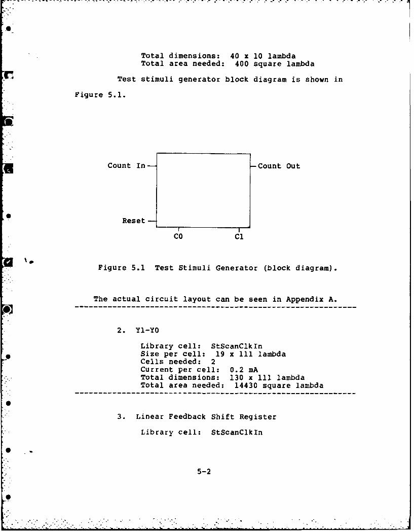
Total dimensions: 40 x 10 lambdaTotal area needed: 400 square lambda
Test stimuli generator block diagram is shown in
Figure 5.1.
Count In -Count Out
Reset
CO Cl
Figure 5.1 Test Stimuli Generator (block diagram).
The actual circuit layout can be seen in Appendix A.
2. Yl-YO
Library cell: StScanClkInSize per cell: 19 x 111 lambdaCells needed: 2Current per cell: 0.2 mATotal dimensions: 130 x 111 lambdaTotal area needed: 14430 square lambda
3. Linear Feedback Shift Register
Library cell: StScanClkIn
5-2
• . ."S " . - i i - - . " "" . . . q ' .
Size per cell: 19 x 113 lambdaCells needed: 8Current per cell: 0.2 mATotal dimensions: 152 x 111 lambdaTotal area needed: 16,872 square lambda
Cell (non-library): Exclusive-OR gateSize per cell: 157 x 95 lambdaCells needed: 3
A block diagram of the linear feedback shift register is
shown in Figure 5.2.
IN
EXOR 1
Out7 Out6 Out5 Out4 Out3 Out2 Outl OutO
EXOR 2
EXOR 3
Figure 5.2 Linear Feedback Register (block diagram).
5-3

I.
The actual circuit layout of the exclusive or gate and
the linear feedback shift register can be seen in Appendix
A.
4. Reference Register and Comparator
The register and comparator function is implemented as a
PLA. The PLA inputs will include the test stimuli values,
the primary outputs of the traffic controller logic, and the
circuit signature. If the signature is correct at specified
clock periods, the go/no go signal will stay high.
Otherwise, the go/no go signal; will be low indicating a
fault. A more detailed description of the testing circuitry
is presented in the test procedure and in Appendix D.
5. PLA for Traffic Controller Function
As stated previously, this PLA will represent any type
of combinational or sequential logic which performs the
traffic controller function. The equations for this PLA are
found in Appendix D.
5-4
6. Clock
Library cell: NClkSize per cell: 100 x 179 lambdaCells needed: 1Current per cell: 1.2 mA
7. Input Pads
Library cell: NIn8Size per cell: 100 x 132 lambdaCells needed: 9Current per cell: 0.3 mA
8. Output Pads
Library cell: NOut8Size per cell: 100 x 145 lambdaCells needed: 6Current per cell: 1.6 mA
9. Vdd Pad
Library cell: NVddSize per cell: 80 x 100 lambdaCells needed: 1Current per cell: 20 mA
10. Gnd Pad
Library cell: NGndSize per cell: 100 x 106 lambdaCells needed: 1Current per cell: 40 mA
11. Substrate Pad
Library cell: NBlank
5-5
'° ' ". * .'
""* ' ' ' "" '/ " ' " * .' .' ' " "' ""
Size per cell: 100 x 106 lambdaCells needed: 1r Current per cell: mA
The final chip block diagram is shown in Figure 5.3
I5
0
5-6
0
traffic3 controller
primaryTest Stimuli inputsGenerator
counter Controllerreset
PLA -----
feedback _------_
disconnect
next statefeedback 5
trafficpresent controller
Linear istate primaryFeedback I outputs
go/no gosignal
Comparator
Figure 5.3 Final block diagram for complete chip design.
5-7

0 t
The actual chip layout can be seen in Appendix B.
Test Procedure and Scenario
In order to test the traffic controller function, it is
necessary to perform the sequence of steps indicated in this
test procedure.
The steps are as follows:
a. Break the traffic controller PLA feedback path
using the feedback disconnect signal. By eliminating theS
feedback, the circuit state can be controlled using external
stimuli.
b. Reset the test stimuli generator using the
counter reset signal.
c. Increment the test stimuli generator, thereby
applying inputs to the traffic controller circuitry.
d. At the same time as step (c), apply valid
primary inputs to the traffic controller circuitry. The LO
and Li registers will be updated with output data
automatically.
e. Select the scan path mode of operation using
the psil and psi2 signals. These signals will clock
information from LO and L1 to the linear feedback shift
5-8

register.
f. Clock the contents of Li and L2 to the linear
feedback shift register.
g. The linear feedback shift register signature is
automatically extracted at this point and input into the
comparator PLA along with the primary outputs from the
traffic controller PLA and the test stimuli generator
outputs. The correct combination of these inputs will yield
a high on the go/no go signal indicating that the circuit is
functioning properly.
h. Return to step (c) a specified number of times
as shown below.
£ ~This procedure must be repeated a predetermined number
of times and with a set of predetermined inputs and test
stimuli. This is because the test results are
pre-programmed into the comparator PLA. The correct order
and values of the test inputs are shown in Table 5.1 along
with the corresponding test output values for a correctly
functioning circuit.
I
5-9

|-I
Test Inputs I Outputs
Test Primary I Next Primary LFSRStimuli Inputs I State Outputs Signature
Cl CO P12 PI1 PIO I YO YI P04 P03 P02 P01 P0
0 1 X X 0 110 0 1 0 0 1 010000001 0 X X 010 1 0 0 1 1 0 1001000011 0 X X i 0 1 1 0 0 0 011001000 1 X X 110 0 1 1 0 0 1 110110011 0 X X 1l 1 1 1 0 1 1 0 00110110I I x 1 X i 0 1 1 0 0 0 01001101I I 1 0 x i 0 1 0 0 0 110100110 0 1 1 X 0 1 1 0 0 1 0 0011010000 0 0 0 0 0 1 0100100 0 X 0 X 0 0 0 0 0 1 0 00110011
Table 5.1 Test generation data for self-test.
The data must be input according to Table 5.1 in order
for the self-test circuitry to work properly.
5-10

6. EVALUATION OF SELF-TEST
This chapter evaluates the self-test testability concept
versus traditional methods of circuit testing. Although no
empirical comparisons are made, clear conclusions can be
drawn relative to viability of each method considering the
1application in mind.
There are three categories which are evaluated. They
are:
a. The effort needed to design the circuit.
b. The layout area used to place the design on a VLSI
chip.
c. The effort involved in testing the completed
circuit.
Each of these categories are discussed as well as
* indications as to which design method would be preferred in
light of the results from the design in Chapter 5.
S
Design Effort
The design of the traffic controller in Chapter 5 is
quite simple. A programmable logic array comprises the
6-1

entire circuit. However, the testing circuitry is much more
extensive. At first glance, this may seem to be a great
hindrance to the self-test concept. However some important
facts must be considered.
First, although the self-test circuitry was much harder
to design than the circuit implementing the traffic
controller function, most of the self-testing circuitry
consists of standard devices which can be used
interchangeably between VLSI chips. For example, the linear
feedback shift register is a basic design technique which
can be used in any self-test circuit. Therefore, it is only
designed once and then transferred to any circuit in which
the need for one arises. The same can be said about the
test stimuli generator. As long as a pseudo-random test
input is acceptable, the counter used in Chapter 5 can be
used again for another circuit. If deterministic test
inputs are needed, much more time and effort would have to
be allocated for the design and test phase. This must be
taken into account.
Second, in Chapters 3 and 4, much effort was made to
emphasize the fact that the traffic controller was being
implemented as a PLA in order to reduce the design effort
for the circuit. However, no matter whether the circuit was
designed as a gate array or whether it was designed at the
6-2

SSI level, the test circuitry would not have changed
(assuming propagation delay was not a problem).
As long as the inputs and outputs of the circuit to be
tested are constant, the test circuitry will not change. In
terms of a practical design effort, this fact has important
implications. It means as long as the primary circuit inputs
and outputs are agreed upon early in the design phase, the
design of the primary circuit and the design of the test
circuitry can be accomplished in parallel. This could mean
months of effort saved, especially for a complex design. In
the world of defense contracts, months of effort could save
the government millions of dollars in R&D costs alone.
The major design effort for the test circuitry in Chapter
5 was the comparator function. Although the comparator
circuit is quite simple (a PLA) the effort involved in
preparing the PLA equations was extensive. Also, it must be
pointed out that the more encompassing the test vectors are
to be, the more effort will be needed to design the
comparator circuit. However, while this may seem time
consuming, the LSSD design principle makes this work very
straightforward.
The design effort for each of the circuit elements is
shown in the following taLle.
6-
[ 6-3
I..
A ""U 2
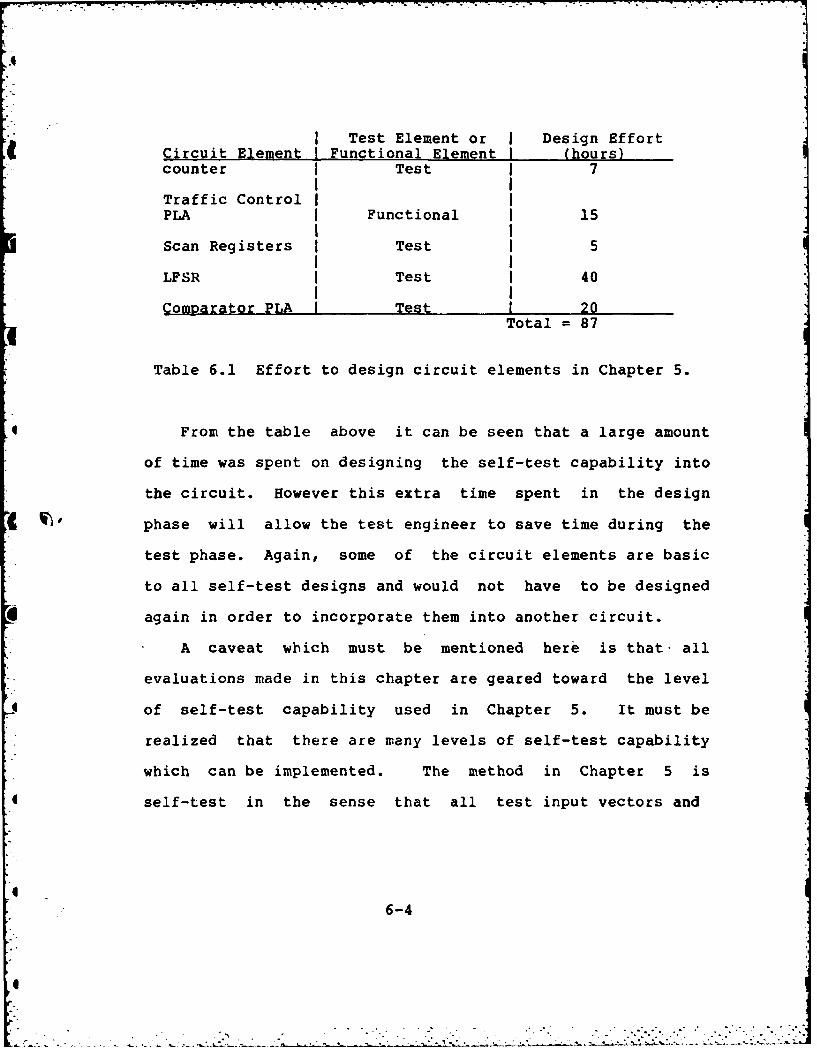
Test Element or Design EffortCircuit Element I Functional Element I (hours)counter Test 7
Traffic ControlPLA Functional 15
Scan Registers Test 5
LFSR Test 40
Comparator PLA Test 20Total = 87
Table 6.1 Effort to design circuit elements in Chapter 5.
From the table above it can be seen that a large amount
of time was spent on designing the self-test capability into
the circuit. However this extra time spent in the design
I ' phase will allow the test engineer to save time during the
test phase. Again, some of the circuit elements are basic
to all self-test designs and would not have to be designed
again in order to incorporate them into another circuit.
A caveat which must be mentioned here is that- all
evaluations made in this chapter are geared toward the level
of self-test capability used in Chapter 5. It must be
realized that there are many levels of self-test capability
which can be implemented. The method in Chapter 5 is
self-test in the sense that all test input vectors and
6-4
I-

V.
comparator functions are included on-chip. The testing
(circuitry does however require external signals such as
feedback disconnect and clocking signals to function
properly. The level of self-test capability could range
from none at all to no external signals required except
power-on. Naturally, the fewer external signals required,
the more complex the self-test circuitry will be. This must
be taken into account during the entire discussion of
self-testing evaluation.
Chip Layout Area
This section discusses the problem of the chip area used
by the self-testing circuitry. The more self-test
capability a circuit has, the more area the testing
circuitry will use.
Consider the circuit layout of the traffic controller in
Appendix B. The testing circuitry covers approximately 88%
of the chip area used by the entire circuit. The following
table shows the chip layout area used by the individual
circuit elements.
6-5
" I i

0L
I Test Element or I Area UsedCircuit Element I Functional Element I (sguare lambda)counter Test 7,000
Traffic ControlPLA Functional 24,300
Scan Registers Test 14,300
LFSR Test 121,900
Comparator PLA Test 40,500Total = 208,000
Table 6.2 Chip layout area used in Chapter 5 design.
From the table above it can be seen that 183,700 square
lambda or 88% of the area used was dedicated to the
self-test capability. Although this figure is rather high
for typical implementations of self-test capability, it is
obvious that circuit layout area will be one of the prices a
designer will have to pay when implementing this concept.
0In the specific case of the traffic controller circuit,
it is obvious that the use of chip area was not a problem.
Even with the self-test circuitry on the chip, the chip area
is not strained for space. However, for a circuit more
complex than the traffic controller, or for a circuit with a
more sophisticated implementation of self-test capability,
space could become a problem. It is then that the designer
must make some decisions as to the relative gains in terms
6
°" 6-6
0

of ease of testing versus problems in chip size or design
effort. This topic is discussed later in this chapter.
Finally, as the device density of VLSI chips grows and
there is a greater tendency to increase the capability of a
circuit on a single chip, then the more difficult it will
become to include self-test circuitry. Although space
limitations are not too critical at the moment, it may be
this characteristic of VLSI design that may keep self-test
from becoming widely accepted.
Test Effort
This section discusses the test effort involved in
testing a circuit designed for self-test versus a circuit
with no self-test capability.
As can be seen in the test procedure in Chapter 5, it is
an easy matter to test the traffic control circuit. No
external comparisons of outputs have to be made. They are
all done automatically. The only output needed to check the
circuit is a go/no go signal. Furthermore, if the self-test
capability were more extensive, possibly nothing would have
to be done to the chip to test it except to apply power to
it. Self-test capability could be expanded so as power is
6-7
Jp
- . . . . . . -- a.. .-.~

applied to the circuit, a self-test firmware routine could
be run. Additionally, if deterministic test input vectors
were needed, they could also be provided using a firmware
routine of some kind (possibly ROM-centered design).
It is obvious that a circuit with self-test capability
is much easier to test than a circuit without such
capability. However, the test engineer may have to do
another type of testing. It is possible that not only does
the chip have to be functionally tested, but also have any
faults located. If this is the case, self-testing circuitry
will not be the answer. Self-testing only indicates if the
circuit is working properly or not. If it is not, no
indication is made as to the location of the fault. This is
a serious drawback for self-testing techniques especially
when the circuit under test is one in which the test
engineer wishes to troubleshoot. This and other problems
will be discussed in the next section.
When To Use Self-Test
This section discusses the conditions and circumstances
when it is advisable to use self-test techniques. Decisions
are made in light of the pros and cons of using self-test
circuitry discussed in the previous sections.
6-8

When the decision is made to add self-testing circuitry
to a primary function circuit, the design effort increases
dramatically. Also, as discussed earlier, the layout area
of the chip could be as much as 88% higher. Finally, the
test results will not give any indication of fault
location. These factors must be considered early in the
design phase. They must be considered in relation to the
application of the primary circuit to determine if the
drawbacks of self-test are worth the gains.
Several conditions must be considered when making the
decision as whether to use self-test or not. They are:
a. What will be the environment for the operation of
the circuit?
b. Will the circuit layout be strained for space?
c. Is controllability and observability important?
Each of these conditions will impact the decision.
The environment for the operation of a circuit is the
single most important consideration when deciding to use
self-test or not.
A critical circuit (e.g. an F-16 fire control circuit)
which must be replaced rapidly (e.g. in a wartime
environment) must check out as working properly at a moments
notice. Manually performing diagnostic checks on a circuit
may result in a weapons system being destroyed before it
6-9

I]
could launch. Self-testing circuits eliminate this delay.
Therefore, for circuits of this type, self-test capability
would be warranted.
Another example of environmental dependency would be a
circuit which is to be used on board a satellite.
Obviously, a technician could not manually test a circuit
once it was in orbit. It is more practical for the
satellite to implement a self-test when ordered and transmit
a go/no go signal to satellite ground controllers.
Self-test is almost imperative in this case.
However, self-test circuitry is not as vital for a
circuit which can be tested without time constraints or
special conditions. An example of this type of circuit may
( , be a disk controller.
Circuit layout area must also be considered. With the
device densities currently available, entire computers can
*be placed on one or two semiconductor chips. Self-test
circuitry for these chips may be impractical because of the
increased layout area needed. The designer may defeat the
whole purpose of one chip computer design by adding the
additional testing area. Again, the decision to use
self-test must be a judgement based on the practicality of
employing it in a given situation.
Another option that the designer has is to incorporate
into a design, a lower level of self-test circuitry.
6-10

Perhaps only enough circuitry can be added to enable the
test engineer to test the circuit manually, but more easilythan normal (e.g. adding pinnouts which are probe points to
the nodes of a circuit which are less observable than other
nodes). The area overhead for this approach would be
minimal.
If controllability and observability are important to
the test engineer, then self-testing will not be
satisfactory. Controllability and observability imply that
a rigorous testing method will be employed (e.g. the
d-Algorithm). It also implies that an attempt will be made
to determine the exact location of a fault and perhaps
repair it. These concepts, while useful under certain
circumstances, do not help a technician trying to determine
if a circuit is functioning in the field. Therefore, the
time to worry about controllability and observability is in
the design of the primary function circuit, not when the
circuit is ready for layout on a chip.
6-11

7. CONCLUSION
The testability of VLSI circuits is an important
consideration during the design phase of a project. As the
device density on VLSI circuits increases, the ability to
test the circuit decreases. Furthermore the effort involved
in testing a circuit once it reaches the field could, and
often does, outweigh the effort involved in the design of
the circuit. As the effort in a project increases, so does
the cost. Therefore, the motivation exists to lessen the
impact of testing on both the schedule and cost of a
project.
£ ~ Several techniques are available to the designer to
measure testability as well as increase testability. Some
of these methods are highly accepted in industry today such
as level sensitive scan design. By adhering to design
methods such as this, the testability of a circuit can be
increased with comparably little extra effort on the design
phase. So successful are some of these techniques that some
companies require their design engineers to incorporate
them.
Other techniques are available whereby dedicated testing 0
circuitry is added to an otherwise completed design. An
7-1
example of this is signature analysis. By using this
technique, a circuits unique response to test stimuli can be
produced on-chip. This enables the tester to determine if
the circuit is working properly by observing the circuits
signature at a predetermined circuit node in response to
test stimuli. Again, this is an industry wide accepted
S-• technique.
By combining level sensitive scan design with signature
analysis a greater level of testability can be realized.
When using both techniques, not only is the circuit more
* testable, but much of the probing a tester would ordinarily
have to do is done automatically, giving the tester a nodal
signature. These signatures are then compared to signatures
obtained from a "good circuit". This implementation of
these techniques shortens the testing phase considerably.
By obtaining signatures at several circuit nodes the
location of a possible fault can also be determined.
Furthermore, this technique can also be used in synchronous
as well as combinational logic. This is due to the ability
of level sensitive scan design to initialize the state of a
synchronous machine to a predetermined starting state.
Finally, the most desirable testing conditions can be
realized by expanding the above technique further. If the
test stimuli and the compare function can be placed on the
7-2
0

|.4
VLSI chip as well, the circuit will be self-testing. The
Conly test output will be a go/no go signal. The drawback to
this method is that the location of a fault cannot be
determined. Depending on the circuit application, this may
I or may not be a priority. The level of sophistication of
self-testing capability can be changed. It must be realized
however that the more self-test capability a circuit has,
the more chip area must be dedicated for this purpose. Each
design must take this into account and a decision must be
made as to the gains of self-test versus the drawbacks.
Several factors should influence the decision of whether
to use self-test circuitry. The most important factor is
the environment in which the circuit is to be tested. A
( ' difficult testing environment is an indication that
self-testing circuitry might alleviate some of the problems
of testing. Also, conditions where testing must be
*accomplished without much time might indicate some self-test
scheme as well. Other factors such as circuit space and
testability measures (controllability and observability)
must also be considered.
As self-test techniques become more standardized and
their use more widespread, the effect on VLSI technology
will be enormous. If all VLSI chips were to incorporate
such designs, the reliability and maintainability of the
7-3
AD-Ai5i 934 DESIGNING VLSI (VERY LARGE SCALE INTEGRATED) CIRCUITS 2/FOR TESTABILITV(U) AIR FORCE INST OF TECHWRIGHT-PATTERSON AFB OH SCHOOL OF ENGINEERING M KAPLAN
UNCLASSIFIED DEC 84 AFIT/GE/ENG/84D-39 F/G 9/5 U
EEEEEEEEEEIIEII flflflflfUl........Ialfllllffffl..
-iii -I 7.1-2
1'..
11111 111W1
MICROCOPY RESOLUTION liST CHART
NAI. NA. , A '. .A~ ,.A.K- ,, '..
• .. .. . • . - • - . -.-. ... - -. -- . . . . - .,- _'----'' c , , , ,

circuits will be improved. In addition, the reliability and
maintainability of the systems they are a part of will also
increase.
As an extension of this thesis, further work should be
undertaken to implement the self-test capability on another
VLSI device. However, unlike this thesis, it should be
totally self-testing. This would involve the implementation
of a sequential machine strictly to run the self-test
feature. In addition, the device should be simulated and
fabricated. Also the function selected should be one which
has previously been designed without self-test capability.
In this way, the two methods of testing can be compared.
7-4

APPENDIX A
CIFPLOTS OF MAJOR SUBSYSTEMS
4
- - - - - - --
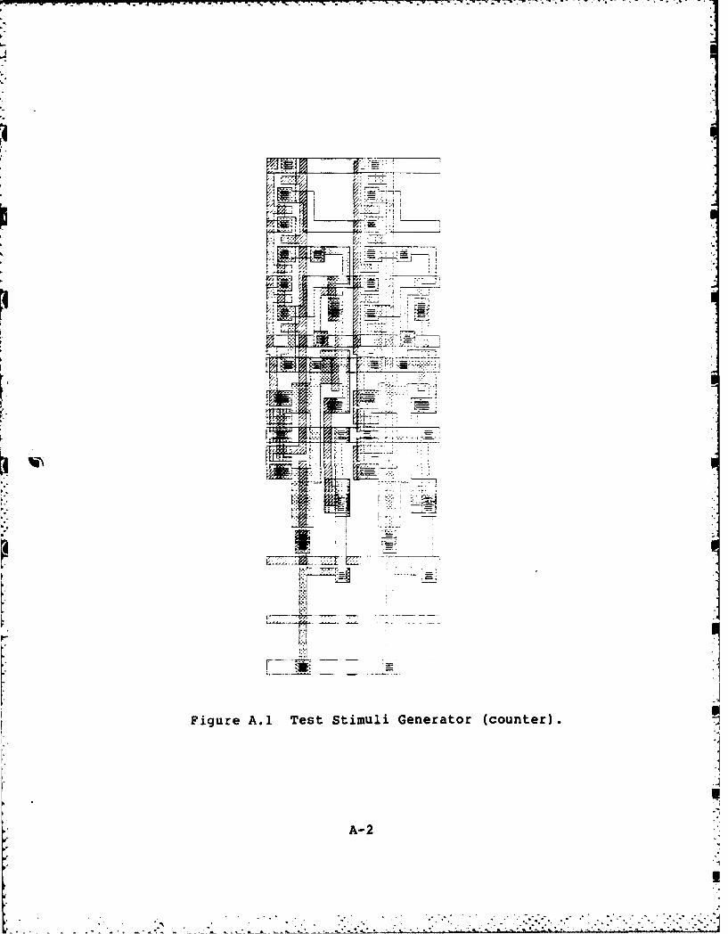
h...
EWa
FiueA1 TsVtmliGnrtr(one)
A-2j
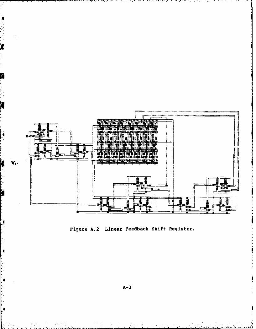
. . . ... .
Figure A.2 Linear Feedback Shift Register.
A-3
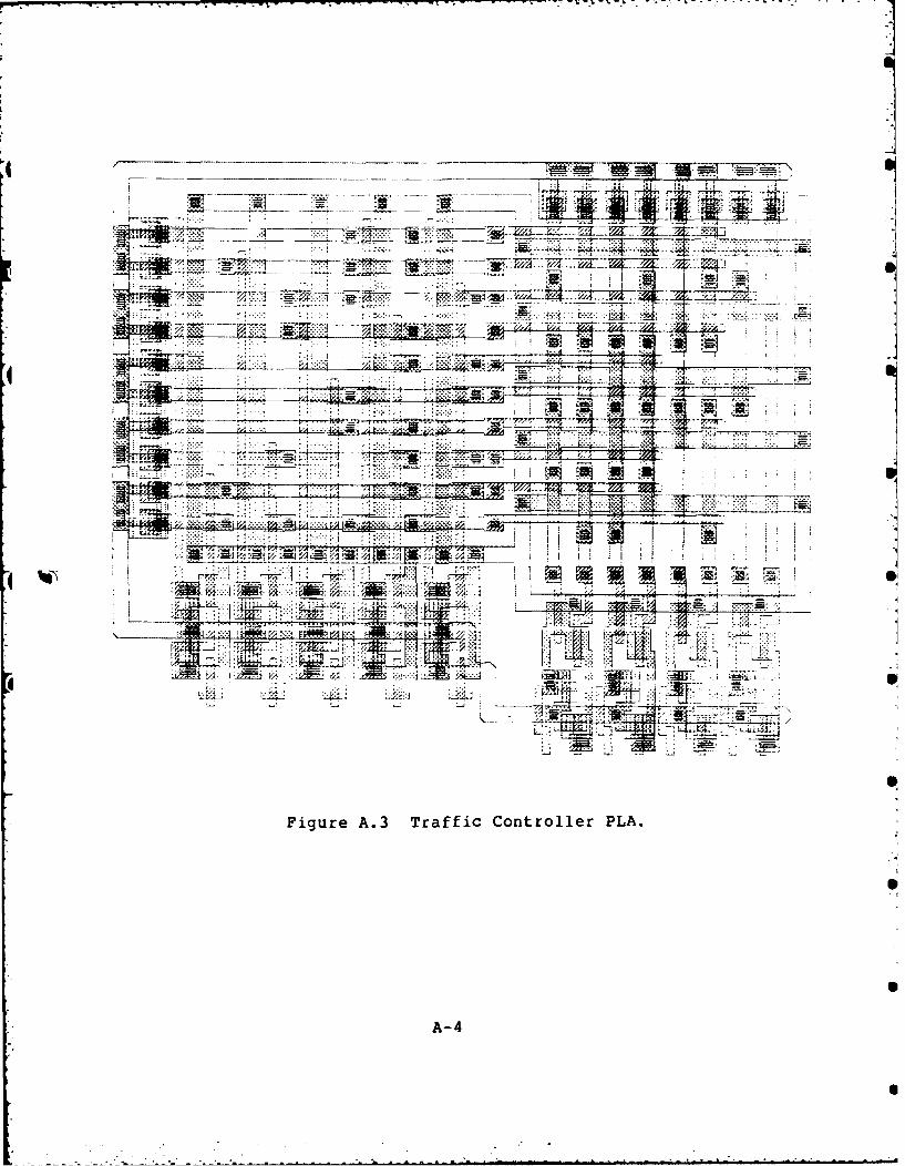
* ~ ~ ~ ~ T 7-. T ~ - ~ _
M _______A
' ;A
Iij
Figure A.3 Traffic Controller PLA.
A-4

Figure A.4 Comparator PLA.
A- 5

APPENDIX B
CIFPLOT OF CHIP LAYOUT
FOR CHAPTER 5 DESIGN
B-1
I
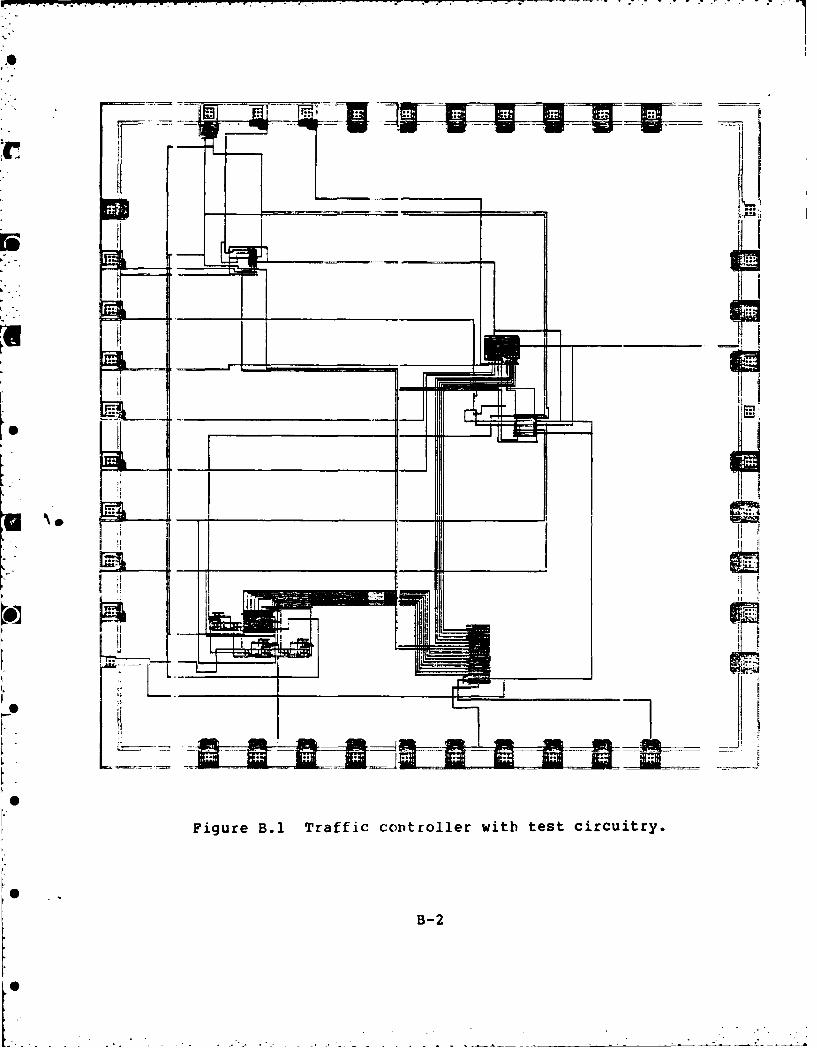
0]
Figure B.1 Traffic controller with test circuitry.
B-2
APPENDIX C
CLL FILES FOR CHAPTER 5 DESIGN
C-1
AND GATEKt
1* cli with -is option *1
#include "/usr/local/cad/lib/s ext.cll"
#define xlen 34#define top 40
andgate
metal;Pnand (0,0);wire metal 0,2 w 4 r 34;wire metal 0,38 w 4 r 34;wire metal 25,0 w 4 u 8;
wire poly 18,59 r 6; */wire poly 18,17 r 6;inverter (22,8);
Pnand /* nand cell */
wire diff 8,4 w 4 u 18;wire diff 8,22 u 14;wire poly 4,9 r 8;wire poly 4,16 r 8;rect 5,23 6,12 implant;rect 5,25 6,8 poly;butt (6,21 rotate 9);wire diff 10,20 r 4;via 6,36 diff; /* Vdd contact */butt (14,18); /* output contact */via 0,7 poly;
via 0,14 poly; /* input contacts */via 6,0 diff; /* ground contact */
inverter
metal;
C-2
[ I. ---. . - -, . . .- --' - -" -- •.- - - . . . . . . , - - -... .. .... ..- ." _ . . . . - ...
~00
wire diff 7,4 u 24;wire poly 4,9 r 6;rect 4,15 6,12 implant;rect 4,17 6,8 poly;butt (5,14 rotate 9);wire diff 5,13 r 8;via 5,28 diff; /* Vdd contact *via 12,11 diff; 1* output contact *via 5,0 diff;
c-
THE CHIP
/* This is the cll file for the entire chip ~
#include '/usr/local/cad/lib/s-ext.cllw#include "padlayout.c11u#include "counter.cill#include lIfsr.cllu#include "inverter2.cllw#include 'wires.c11"external pla3(cif 2000 bounds 0,400 --400,0)external comp(cif 3000 bounds 0,470 --240,0)external StScaraCkln(cif 514 bounds 0,0 19,111)TheChip
Pads (0 ,0) ;LFSR(600,600);CNTR(800,2500);pla3 (2000,2600);coxnp(2500,1000 rotate 3);StScanCkln(2150,1700 rotate 6);StScanCkln(2250,1700 rotate 6);invertergate2 (1950,1800);invertergate2(700,2600);Wires (0,0);
C-4
TWO STAGE COUNTER
#include 0/usr/local/cad/lib/sext.cll'
#define cntr-space_2 24 /* lambda */
CNTR{/* place 2-bit counter */
Cntr_2(300,250);iterate 2,1
CntReset(300,234); /*reset transistors*/
metal;wire 300,227 w 4 r 50; /* GND for reset */wire 310,235 diff w 2 d 10;
/* wires for reset connection *1wire 334,235 diff w 2 d 10;
* via 308,225 diff;via 332,225 diff;
}/* ............................... ..... . ..............
CntReset
" /* reset transistors on counters */wire diff 10,4 d 30;wire poly 0,--20 r 24;
I * ....................... *..... ......... t...... *
Cntr_2{/* two bit count "
iterate 2, 1 cntrspa4e_2, defaultCnt(O, 0);
/* ............................................0.......... /
0
C-5
EXCLUSIVE OR GATE
( /* Exclusive OR gate ~
#include "or.cll"#include "and.c11w#include 'inverter.cll"
ro exorgate
{rae05)orgate(0,0);
invertergate(50,0);4 andgate(l00,0);
/* wires for exor gate *
wire poly 42,71 w 4 r 50 d 55 r 10;wire metal 63,13 w 4 r 10 d 4 r 29;wire metal 32,21 w 4 r 10 d 12 r 10;wire metal 2,9 w 3 1 15 u 59 r 15;wire metal 2,16 w 3 1 5 u 42.5 r 5;via --6,56.5 poly;wire poly --4,58 w 3 1 17;via --22,56 poly;
/* wires for Vdd *
wire metal 32,38 w 4 r 70;wire metal 57,38 w 4 d 10;wire metal 57,38 w 4 u 50 1 18;
/* wires for Gnd *
wire diff 12,54 w 3 d 7 r 30 d 45;via 40,0 diff;wire metal 32,2 w 4 r 70;
invertergate
metal;
wire diff 7,4 u 24;wire poly 4,9 r 6;rect 4,15 6,12 implant;rect 4,17 6,8 poly;
C-6
V
butt (5,14 rotate 9);wire diff 5,13 r 8;via 5,28 diff; /* Vdd contact */via 12,11 diff; /* output contact */via 0,7 poly; /* input contact */via 5,0 diff;
invertergate2
metal;wire diff 7,4 u 24;wire poly 4,9 r 6;rect 4,15 6,12 implant;rect 4,17 6,8 poly;butt (5,14 rotate 9);wire diff 5,13 r 8;via 5,28 diff; /* Vdd contact */via 12,11 diff; /* output contact */via 0,7 poly; /* input contact */via 5,0 diff;
C-7
LINEAR FEEDBACK SHIFT REGISTER
1* Linear Feedback Shift Register *
#include */usr/local/cad/lib/ext.cll"#include 'exor.cll'/*external StScanCkln(cif 514 bounds 0,0 19,111)*/LF SR
StScanCkln(0,0);StScanCkln(19,0);StScanCkIn (3 8,0);StScanCkln(57,O);StScanCkln(76,0);StScanCkln(95,O);StScanCkln(114,0);StScanCkln(133,0);
4 1* Exclusive OR gates *
exorgate(--180,10);exorgate(200,--120 flip ir);exorgate(0,--120 flip ir);
P~ wire from XOR1 to input of register *
wire diff --27,31 w 2 r 12 d 22 r 17;
1* wire from out 7 to XOR3 ~
wire poly 115,111 w 2 u 9 r 229 d 100;via 342,18 poly;wire metal 344,22 w 3 d 75;
P~ wire from out 6 to XOR3 ~
* wire poly 96,111 w 2 u 19 r 258 d 192;
P~ wire from out 8 to XOR2 ~F wire poly 134,111 w 2 u 4 r 40 d 168;via 172,--54 poly;
4 wire metal 175,--52 w 3 1 30;
4
C-8
. . . . . . . . . . . .
/* wire from XOR3 to XOR2 ~
wire metal 203,--99 w 3 1 23 u 37 1 27;
/* wire from XOR2 to XOR1 *
wire metal 3,--99 w 3 1 170 u 119;
/* Vdd wires *
wire metal --25,48 w 4 r 15 u 45 r 11;wire metal --10,52 w 4 d 18 r 11;wire metal --10,50 w 4 d 132 r 11;wire diff 125,--82 w 3 r 87;
1* Gnd wires ~
wire diff --50,13 w 3 d 132;via --52,--120 diff;wire metal --50,--118 w 4 r 53;
q wire metal 130,--118 w 4 r 73;via 188,--120 diff;wire diff 190,--119 w 3 u 30;via 188,--92 diff;wire metal 190,--90 w 4 u 145 1 40;wire metal 190,55 w 4 u 53 1 40;
C-9
HAND GATE
nand /* nand cell */
metal;wire diff 8,4 w 4 u 18;wire diff 8,22 u 14;wire poly 4,9 r 8;wire poly 4,16 r 8;rect 5,23 6,12 implant;rect 5,25 6,8 poly;butt (6,21 rotate 9);wire diff 10,20 r 4;via 6,36 diff; /* Vdd contact */via 14,18 diff; /* output contact */via 0,7 poly;via 0,14 poly; /* input contacts */via 6,0 diff; /* ground contact */
c-10
• • . .
I
norgate /* nor cell */I!
metal;wire diff 12,4 u 2;wire diff 6,7 r 12;wire diff 7,8 u 8;wire diff 17,8 u 8;wire diff 6,17 r 14;wire diff 12,18 u 12;wire poly 4,12 r 6;wire poly 14,12 r 8 d 4;rect 9,18 6,11 implant;rect 9,20 6,7 poly;butt (10,17 rotate 9);via 10,30 diff; /* Vdd contact */via 20,15 diff; /* output contact */via 0,10 poly;via 20,4 poly; /* input contacts */via 10,0 diff; /* ground contact */
1C-11
OR GATE.--.--- %'.-
#def ine xieng 42*def ine yleng 40
orgate
nor (0,4);inverter2 (26,8);
wire metal 0,2 w 4 r ileng;wire metal 0,38 w 4 r xieng;wire metal 0,8.5 r 24;
wire poly 27.25 d 7;wire metal 33,0 w 4 u 8;via 10,0 diff; *N/
nor /*nor cell *
metal;wire diff 12,4 u. 2;wire diff 6,7 r 12;
%A wire diff 7,8 u 8;wire diff 17,8 u 8;wire diff 6,17 r 14;wire diff 12,18 u 12;wire poly 4,12 r 6;wire poly 14,12 r 8 d 4;rect 9,18 6,11 implant;rect 9,20 6,7 poly;butt (10,17 rotate 9);via 10,30 diff; /* Vdd contact *butt(20,15); /* output contact *
via 0,10 poly;via 20,4 poly; 1* input contacts *wire diff 12,4 d 6;
inverter2
metal;wire diff 7,4 u 24;wire poly 4,9 r 6;rect 4,15 6,12 implant;rect 4,17 6,8 poly;
C-12 *

butt (5,14 rotate 9);wire diff 5,13 r 8;via 5,28 diff; /* Vdd contact */butt(12,11); /* output contact */wire poly 0,9 r 4;via 5,0 diff;
I!
-
C1
C-13
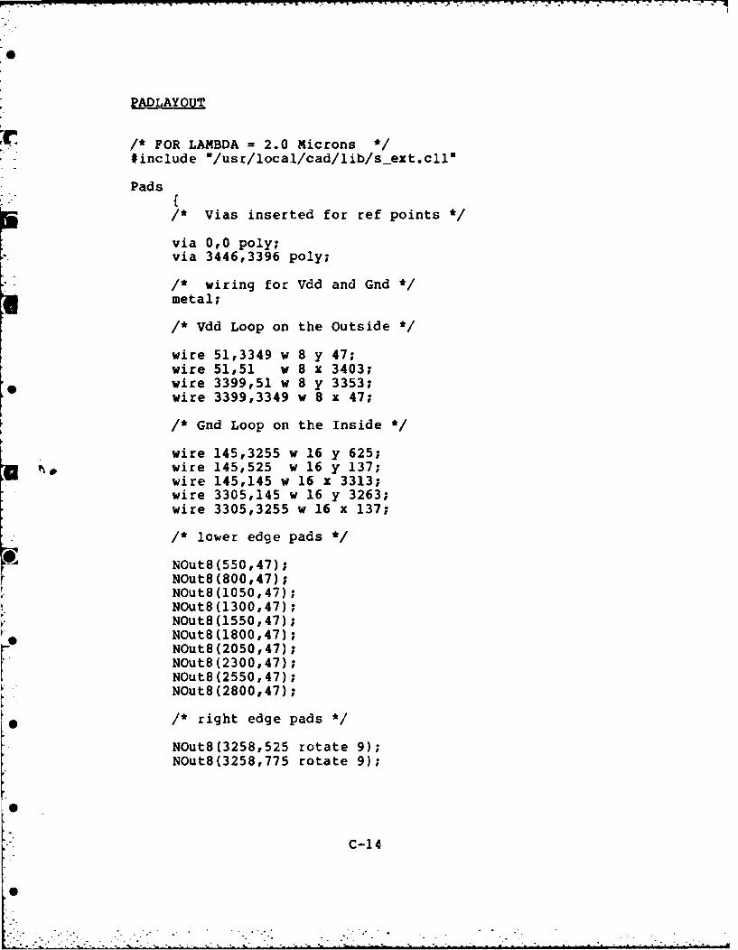
PADLAYOUT
/* FOR LAMBDA = 2.0 Microns */#include "/usr/local/cad/lib/s-ext.c113
Pads {/* Vias inserted for ref points */
via 0,0 poly;via 3446,3396 poly;
/* wiring for Vdd and Gnd /metal;
/* Vdd Loop on the Outside */
wire 51,3349 w 8 y 47;wire 51,51 w 8 x 3403;wire 3399,51 w 8 y 3353;wire 3399,3349 w 8 x 47;
/* Gnd Loop on the Inside */
wire 145,3255 w 16 y 625;wire 145,525 w 16 y 137;wire 145,145 w 16 x 3313;wire 3305,145 w 16 y 3263;wire 3305,3255 w 16 x 137;
/* lower edge pads */
NOutS(550,47);NOut8(800,47);NOut8(1050,47);NOut8(1300,47);NOut8(1550,47);NOut8(1800,47);NOut8(2050,47);NOutS(2300,47);NOut8(2550,47);NOut8(2800,47);
/* right edge pads */
NOut8(3258,525 rotate 9);NOut8(3258,775 rotate 9);
C-14
".-
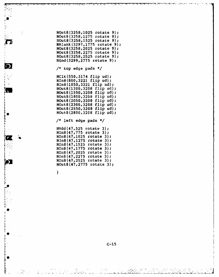
- NOut8(3258,1025 rotate 9);NOut8(3258,1275 rotate 9);NOut8(3258,1525 rotate 9);NBlank(3297,1775 rotate 9);NOut8(3258,2025 rotate 9);NOutS(3258,2275 rotate 9);NOut8(3258,2525 rotate 9);NGnd(3299,2775 rotate 9);
1* top edge pads *
NClk(550,3174 flip ud);NIn8(800,3221 flip ud);NIn8(1050,3221 flip ud);NOut8(1300,3208 flip ud);NOut8(lBOO,3208 flip ud);NOut8(1550,3208 flip ud);
N~u8(250,208flip ud);N~ut823003208flip tid);
NOutB(2550,3208 flip ud);*NOut8(2800,3208 flip ud);
/* left edge pads *
* - NVdd(47,525 rotate 3);NIn8(47,775 rotate 3);NInB(47,1025 rotate 3);
FNIn8(47,1275 rotate 3);*-NInB(47,1525 rotate 3);
-NIn8(47,1775 rotate 3);NIn8(47,2025 rotate 3);NIn8(47,2275 rotate 3);NIrxB(47,2525 rotate 3);NOut8(47,2775 rotate 3);
0
C-15
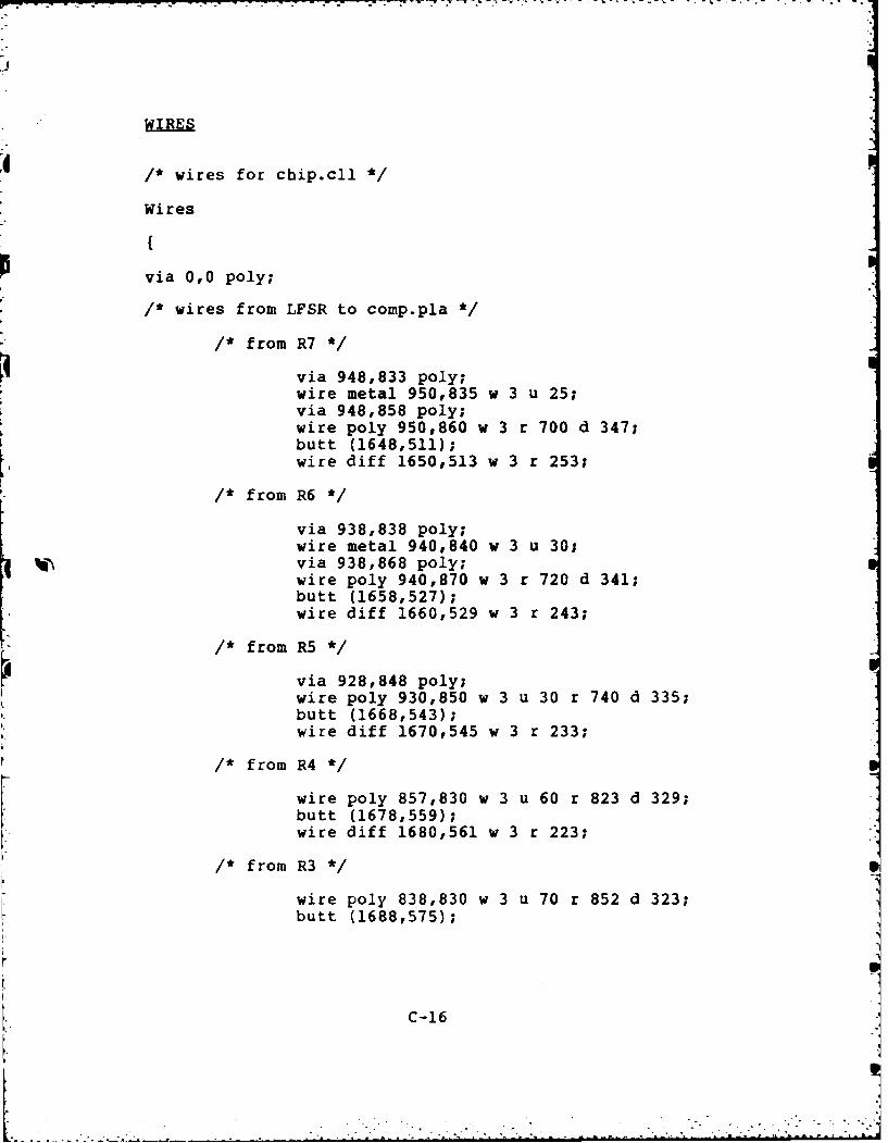
WIRES
/* wires for chip.cll */
Wires
{
via 0,0 poly;
/* wires from LFSR to comp.pla */
/* from R7 */
via 948,833 poly;wire metal 950,835 w 3 u 25;via 948,858 poly;wire poly 950,860 w 3 r 700 d 347;butt (1648,511);wire diff 1650,513 w 3 r 253;
/* from R6 */
via 938,838 poly;wire metal 940,840 w 3 u 30;via 938,868 poly;wire poly 940,870 w 3 r 720 d 341;butt (1658,527);wire diff 1660,529 w 3 r 243;
/* from R5 */
via 928,848 poly;wire poly 930,850 w 3 u 30 r 740 d 335;butt (1668,543);wire diff 1670,545 w 3 r 233;
/* from R4 */
wire poly 857,830 w 3 u 60 r 823 d 329;butt (1678,559);wire diff 1680,561 w 3 r 223;
/* from R3 */
wire poly 838,830 w 3 u 70 r 852 d 323;butt (1688,575);
C-16
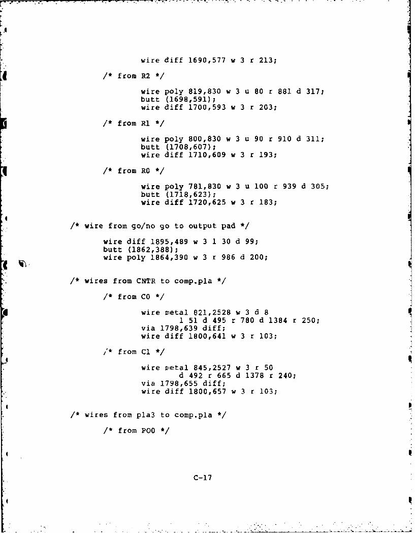
wire diff 1690,577 w 3 r 213;
/* from R2 */
wire poly 819,830 w 3 u 80 r 881 d 317;butt (1698,591);wire diff 1700,593 w 3 r 203;
/* from R1 */
wire poly 800,830 w 3 u 90 r 910 d 311;butt (1708,607);wire diff 1710,609 w 3 r 193;
/* from RO */
wire poly 781,830 w 3 u 100 r 939 d 305;butt (1718,623);
wire diff 1720,625 w 3 r 183;
/* wire from go/no go to output pad */
wire diff 1895,489 w 3 1 30 d 99;butt (1862,388);wire poly 1864,390 w 3 r 986 d 200;
/* wires from CNTR to comp.pla */
/* from CO */
wire metal 821,2528 w 3 d 81 51 d 495 r 780 d 1384 r 250;
via 1798,639 diff;wire diff 1800,641 w 3 r 103;
' from Cl1
wire metal 845,2527 w 3 r 50d 492 r 665 d 1378 r 240;
via 1798,655 diff;wire diff 1800,657 w 3 r 103;
/* wires from pla3 to comp.pla */
/* from PO0 */
C-17
wire diff 2127,2063 w 2d 73 1 377 d 1317 r 153;
/* from P01 */
wire diff 2133,2063 w 2d 83 1 373 d 1291 r 143;
/* from P02 *1
wire diff 2142,2063 w 2d 93 1 372 d 1265 r 133;
/* from P03 */
wire diff 2148,2063 w 2d 103 1 368 d 1239 r 123;
/* from P04 */
wire diff 2158,2063 w 2d 113 1 367 d 1213 r 113;
/* wire from pla3 output to Li */
wire diff 2118,2063 w 2 d 13;via 2116,2048 diff;
wire metal 2118,2050 w 3 d 110;via 2116,1938 diff;wire diff 2118,1940 w 2 r 139 d 131;
/*- wire from pla3 output to L.0 *
wire diff 2112,2063 w 2 d 23;via 2110,2038 diff;wire metal 2112,2040 w 3 d 110;via 2130,1928 diff;wire diff 2112,1930 w 2 r 45 d 121;
/* wire from pla3 input to LO */
wire diff 2087,2063 w 2 d 20;via 2085,2041 diff;wire metal 2087,2043 w 3 d 120;
C-18
via 2085,1921 diff;wire diff 2087,1923 w 2 d 240 r 82;butt (2167,1681);wire poly 2169,1683 w 3 u 19;
/* wire from pla3 input to Li */
wire diff 2071,2063 w 2 d 30;via 2069,2031 diff;wire metal 2071,2033 w 3 d 110;via 2069,1921 diff;wire diff 2071,1923 w 2 d 250 r 198;butt (2267,1671);wire poly 2269,1673 w 3 u 29;
/* wire from LO to Li */
wire diff 2168,1802 w 3 r 85;
/* wire from LO to LFSR */
wire diff 2152,1802 w 2 1 20;via 2130,1800 diff;wire metal 2132,1802 w 3 1 100 d 100 1 370;via 1680,1700 diff;wire diff 1682,1702 w 3 1 1080;via 600,1700 diff;wire metal 602,1702 w 3 d 915;
/* wires from pla3 to input pads */
wire diff 2055,2063 w 2 d 57 1 350 d 476 1 1200;via 503,1528 diff;wire metal 505,1530 w 3 1 330;wire diff 2039,2063 w 2 d 47 1 350 d 236 1 284;via 1403,1778 diff;wire metal 1405,1780 w 3 1 1230;wire diff 2023,2063 w 2 d 10 1 1317;via 704,2051 diff;wire metal 706,2053 w 3 d 23 1 530;
S/* wire for counter reset */
wire poly 802,2515 w 2 1 70 u 15;
C-19
via 730,2528 poly;
wire metal 732,2530 w 3 1 558;
/* wires from counter to pla3 *1
/* from CO */
via 1548,1928 diff;wire diff 1550,1930 w 3 r 37;via 1585,1928 diff;wire metal 1587,1930 w 3 r 250;via 1835,1928 diff;wire diff 1837,1930 w 3 r 250;via 2085,1928 diff;
/* from C1 */
wire metal 1559,1940 w 3 r 286;via 1843,1938 diff;wire diff 1845,1940 w 3 r 226;
4 via 2069,1938 diff;
/* wires for feedback disconnect */
/* from inverter to input pad */
wire metal 1953,1809 w 3 1 8 u 470;via 1943,2277 diff;wire diff 1945,2279 w 3 1 1500;via 443,2277 diff;wire metal 445,2279 w 3 1 269;
/* frow inverter to pass transistor */
wire metal 1963,1812 w 3 r 20 u 40;via 1981,1850 poly;wire poly 1983,1852 w 3 r 125;
/* from feedback disconnect line to pass transistor*/
via 1943,1898 poly;wire poly 1945,1900 w 3 r 15 u 45;
C-20
/* wires for shifting signal */
/* from pad 4 to LFSR for psi2 t/
wire metal 930,799 w 4 r 12;via 940,797 diff;wire diff 942,799 w 3 d 149;via 940,648 diff;wire metal 942,650 w 3 d 30;via 940,618 diff;wire diff 942,620 w 3 d 50 1 392 u 710;via 548,1278 diff;wire metal 550,1280 w 3 1 375;
/* from LO to Ll to connect ps12 */
wire metal 2168,1732 w 4 r 85;
/* from LO & Li to pad 4 */
wire metal 2268,1732 w 3 r 40 d 452 1 608;via 1698,1278 diff;wire diff 1700,1280 w 3 1 1150;
/* from pad 3 to LFSR psil1
wire metal 930,730 w 4 r 7 d 25 1 152;via 783,703 diff;wire diff 785,705 w 3 1 40;via 743,703 diff;wire metal 745,705 w 3 1 30;via 713,703 diff;wire diff 715,705 w 3 1 125;via 588,703 diff;wire metal 590,705 w 3 u 325 1 415;
/* from LO to Ll to connect psil */
wire metal 2168,1800 w 4 r 85;
/* from LO & L1 to pad 3 */
wire metal 2268,1800 w 3 r 50 d 770 1 625;via 1691,1028 diff;wire diff 1693,1030 w 3 1 1103;via 588,1028 diff;
C-21
0. . . . . - . .. . - , _ . . . i . . . - " , "
A
/* wires to increment counter */
/* from pad T2 to inverter */
wire metal 895,3221 w 3 d 20 1 210d 592 r 17;
/* from inverter to CINbar */
wire metal 713,2613 w 3 r 12 u 9 r 77;
/* from pad T2 wire to CIN */
wire metal 685,2660 w 3 1 20 d 100r 80 u 47 r 57;
/* wire to introduce VDD */
wire metal 100,575 w 30 r 200;
/* wires for phil and phi2 */
/* from phil to CNTR phil */
wire metal 580,3177 w 3 d 632 r 170 d 14;via 748,2529 poly;wire poly 750,2531 w 3 r 52;
/* from phi2 to CNTR phi2 */
wire metal 622,3177 w 3 d 77;via 620,3098 diff;wire diff 622,3100 w 3 r 100;via 720,3098 diff;wire metal 722,3100 w 3 r 148 d 509 1 24;
6 /* from LO phil to Li phil */
wire metal 2168,1808 w 3 r 85;
/* from LO & L1 phil to pad phil */
wire metal 2268,1808 w 3 r 40 u 992 1 1408;via 898,2798 diff;wire diff 900,2800 w 3 1 300;via 598,2798 diff;
C-22
aA
wire metal 600,2800 w 3 1 20;
/* from LO phi2 to Li phi2 */
wire metal 2168,1793 w 3 r 85;
/* from LO & Li phi2 to pad phi2 */
wire metal 2268,1793 w 3 r 10;via 2276,1791 diff;wire diff 2278,1793 w 3 r 50 u 50 1 10;via 2316,1841 diff;wire metal 2318,1843 w 3 u 970 1 1448;
/* from LFSR phil to pad phil */
wire metal 781,724 w 3 d 9;via 779,713 diff;wire diff 781,715 w 3 1 26;via 753,713 diff;wire metal 755,715 w 3 1 125;via 628,713 diff;wire diff 630,715 w 3 1 60;via 568,713 diff;wire metal 570,715 w 3 1 170;via 398,713 diff;wire diff 400,715 w 3 u 1885;via 398,2598 diff;wire metal 400,2600 w 3 r 180;
/* from LFSR phi2 to pad phi2 */
wire metal 930,738 w 3 r 32;via 960,736 diff;wire diff 962,738 w 3 r 48;via 1008,736 diff;wire metal 1010,738 w 3 u 52 r 150 d 290;via 1158,498 diff;wire diff 1160,500 w 3 1 770 u 2635 r 232;via 620,3133 diff;
/* Vdd wires */
/* Vdd pad to LFSR *1
wire metal 290,575 w 3 r 250 d 50 r 100 u 60;via 638,583 diff;wire diff 640,585 w 3 u 53;
C-23
via 638,636 diff;
wire metal 640,638 w 3 r 130;
/* Vdd pad to comp.pla *1
wire metal 290,575 w 3 d 170 r 1810u 90 1 75;
/* Vdd from comp.pla to LO and Li */
wire metal 2100,495 w 3 r 450 u 1222;via 2548,1715 diff;wire diff 2550,1717 w 3 1 260;via 2288,1715 diff;wire metal 2290,1717 w 3 1 22;wire diff 2550,1717 w 3 u 59 1 260;via 2288,1774 diff;wire metal 2290,1776 w 4 1 22;
/* Vdd from LO to Li */
wire metal 2168,1717 w 4 r 85;wire metal 2168,1776 w 4 r 85;
/* Vdd from LO to inverter */
wire metal 2152,1776 w 3 1 102;via 2048,1774 diff;wire diff 2050,1776 w 3 1 150 u 54 r 58;
/* Vdd from L1/comp wire to pla3 */
wire diff 2390,1776 w 3 u 450 1 340;via 2048,2224 diff;wire metal 2050,2226 w 3 d 29;
/* Vdd from pla3/L1 wire to CNTR */
wire metal 2050,2226 w 4 u 339 1 1205;via 898,2563 diff;wire diff 900,2565 w 3 u 73 1 45;via 853,2636 diff;wire metal 855,2638 w 4 1 10;
/* Vdd from CNTR to inverter */
wire metal 802,2638 w 4 1 95 d 7;
C-24
/* GND wires ~
/* to inverter (CNTR) *
wire metal 145,2500 w 4 r 562;via 705,2498 diff;wire diff 707,2500 w 4 u 102;
1* from inverter GND wire to CNTR *
wire diff 706,2584 w 4 r 60;via 764,2582 diff;wire metal 766,2584 w 4 r 35;
4 1* from inverter GND wire to CNTR reset GND *
wire diff 705,2502 w 4 r 80;via 783,2500 diff;wire metal 785,2502 w 4 r 20;
* 1* to pla3 *
wire metal 2177,2150 w 4 r 23;via 2198,2148 diff;wire diff 2200,2150 w 4 r 170;via 2368,2148 diff;wire metal 2370,2150 w 4 r 935;4
/* LO to LI GND wires ~
wire metal 2168,1703 w 4 r 85;wire metal 2168,1756 w 4 r 85;
* via 2178,1701 diff;via 2178,1754 diff;wire diff 2180,1703 w 4 u 55;
/* f ron Li to pla3 *
* wire metal 2268,1756 w 4 r 22;via 2288,1754 diff;wire diff 2290,1756 w 4 r 160;via 2448,1754 diff;wire tmetal 2450,1756 w 4 u 395;
* /* from inverter to LO ~
wire metal 1957,1802 w 4 d 46;via 1955,1754 diff;
C-25
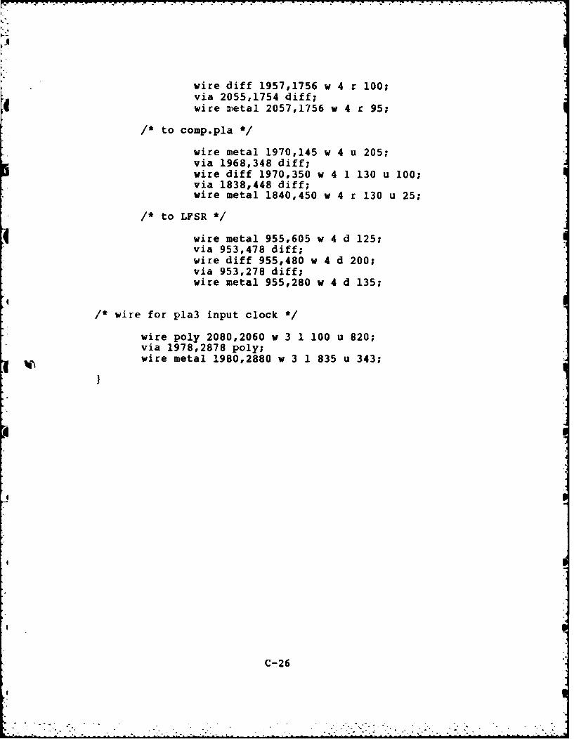
wire diff 1957,1756 w 4 r 100;via 2055,1754 diff;wire metal 2057,1756 w 4 r 95;
/* to comp.pla */
wire metal 1970,145 w 4 u 205;via 1968,348 diff;wire diff 1970,350 w 4 1 130 u 100;via 1838,448 diff;wire metal 1840,450 w 4 r 130 u 25;
/* to LFSR */
wire metal 955,605 w 4 d 125;via 953,478 diff;wire diff 955,480 w 4 d 200;via 953,278 diff;wire metal 955,280 w 4 d 135;
/* wire for pla3 input clock */
wire poly 2080,2060 w 3 1 100 u 820;via 1978,2878 poly;wire metal 1980,2880 w 3 1 835 u 343;
C-26

K APPENDIX D
In order to produce a PLA using the CAD tools available
at AFIT, one must first produce a set of equations which
will be called a ".equ" file. This file is then run through
eqntott, which is another CAD tool. The output of eqntott
4is a file marked with the extention m.prein". This file is
then run through the PLA generator called "mkpla".
The following sets of equations represent the .equ files
*for the PLA's used in the design in Chapter 5.
.egu File for the Traffic Controller
INORDER =C TL TS yl yO;
* OUTORDER =YO Yl ST BLO HLl FLO FLl;
YO = (TS & !yO & yl) I (C & !TL & yO &yl) I(IC &yO &yl)I MT & yO & yl) I (ITS & yO & lyl);
Yl = (C & TL & IyO & !yl) I (ITS &IyO & yl)* I(TS & IyO & yl) I (C & ITL &yO & yl);
ST= (C & TL & IyO & Iyl) I (IC yO & yl) I (IC yO Lyl)I(TL & yO & yl) I (TS & yO & yl);
ELO = (C & ITL & yO & yl) I(IC &yO &yl) I(TL &yO &yl)*I(ITS & yO & yl) I(TS &yO & yl);
fiLl = (ITS &IyO &yl) I(TS &!yO &yl);
D-1
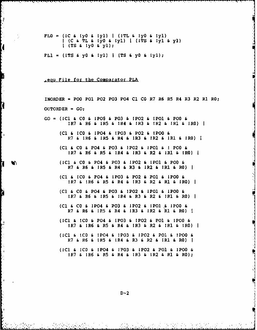
FLO = (IC & IyO & !yl) I (ITL & lyO & lyl)I (C & TL & lyO & lyl) I (ITS & lyl & yl)I (TS & !yO & yl);
FL1 = (ITS & yO & lyl) I (TS & yO & lyl);
-eau File for the Comparator PLA
INORDER = P0 P01 P02 P03 P04 Cl CO R7 R6 R5 R4 R3 R2 RI RO;
OUTORDER = GO;
GO = (IC1 & CO & IPO$ & P03 & IP02 & IPOl & PO0 &IR7 & R6 & IR5 & IR4 & IR3 & !R2 & !Ri & IRO)
(Cl & ICO & IP04 & !P03 & P02 & IPOO &R7 & 1R6 & IR5 & R4 & IR3 & IR2 & IRI & IRO)
(Cl & CO & P04 & P03 & IP02 & IPO1 & I PO0 &IR7 & R6 & R5 & R4 & IR3 & R2 & IR1 & IRO)
(ICI & CO & P04 & P03 & !P02 & IPO & PO0 &R7 & R6 & IR5 & R4 & R3 & IR2 & IRI & RO) I
(Cl & ICO & P04 & IP03 & P02 & P01 & IPOO &IR7 & !R6 & R5 & R4 & IR3 & R2 & Ri & IRO) I
(Cl & CO & P04 & P03 & IP02 & IPOl & IPOO &!R7 & R6 & IR5 & IR4 & R3 & R2 & :Ri & RO) I
(Cl & CO & IP04 & P03 & IP02 & IPO *& IPOO &R7R & 5 & !04 & R4 & IR2 & R1 & RO) &
(IC & R & PO4 & R4 & P 3 & P02 & P01 & IPO)IR7 & IR6 & R5 & R4 & IR3 & R2 & IR1 & IRO)
(IC1 & ICO & !P04 & IP03 & IP02 & POI & IPOO &R7 & R6 & IR5 & IR4 & R3 & R2 & IR1 & RO) I
(ICi & ICO & IP04 & !P03 & IP02 & P01 & IPOO &!R7 & !R6 & R5 & R4 & IR3 & IR2 & Ri & RO);
D-2

Bibliography
1. Bennetts, R. G. Design of Testable Logic Circuits.London: Addison-Wesley, 1984.
2. Berg, William C. and Robert D. Hess, "COMET: ATestability Analysis and Design ModificationPackage," Proceedings of the 1982 InternationalTest Conference. 364-378. IEEE Press, Silver Spring,MD, 1982.
3. Bhaskar, K. S., "Signature Analysis: Yet AnotherPerspective," Proceedings of the 1982 InternationalTest Conference. 132-134. IEEE Press, Silver Spring,MD, 1982.
4. Chang, Herbert Y., Eric Manning, and Gernot MetzeFault Diagnosis of Digital Systems. New York:WlFey-Interscience, 1970.
5. Eichelberger, E. B. and T. W. Williams, "A Logic Design
Structure for LSI Testability," Proceedings of the 14thDesign Automation Conference. 462-468. IEEE Press,New York, June, 1977.
6. Friedman, Arthur D., Premachandran R. MenonFault Detection in Digital Circuits., 1971.
7. Hayes, John P. and Edward J. McCluskey "TestabilityConsiderations in Microprocessor-Based Design,"Computer, 13: 17-26 (March 1980).
* 8. Komonytsky, Donald, "LSI Self-Test Using LevelSensitive Scan Design and Signature Analysis,"Proceedings of the 1982 International Test Conference.
414-424. IEEE Press, Silver Springs, MD, 1982.
9. Konemann, Bernd, Joachim Mucha, and Gunther Zwiehoff,"Built-In Logic Block Observation Techniques,"Proceedings of the 1979 Test Conference. 37-41. IEEEPress, New York, N.Y., 1979.
10. Kovijanic P. G., "Testability Analysis," Proceedingsof the 1979 Test Conference. 310-316. IEEE Press,New York, N.Y., 1979.
BIB-i
jI.,

11. Ratiu, Ion M., Alberto Sangiovanni-Vincentelli, andDonald 0. Pederson, "VICTOR: A Fast VLSI TestabilityAnalysis Program," Proceedings of the 1982International Test Conference. 397-401. IEEEPress, Silver Springs, MD, 1982.
12. Susskind, Alfred K. Testability and Reliability ofLSI, 15 September 1973--31 July 1980. RADC-TR-80-384.Rome Air Development Center, Rome, N.Y., January 1981(AD-A096 310).
13. Williams, T. W. and Kenneth P. Parker *Testing LogicNetworks and Designing for Testability," Computer,12: 9-12 (October 1979).
-BIB-2
Ib"
0'
6O

VITA
Captain Michael Kaplan was born on 25 January 1958 in
Boston, Massachusetts. He graduated from high school in
Randolph, Massachusetts, in 1975 and attended Southeastern
Massachusetts University from which he received the degree
of Bachelor of Science in Electrical Engineering in June
1979. In February 1980, he received a commission in the
USAF through Officer Training School. Following OTS he was
assigned to Hanscom AFB and served there in the Deputy for
Development Plans. His next assignment was at Los Angeles
AFS where he served in the Deputy for Space Navigation
Systems as a software and contract manager, until entering
the School of Engineering, Air Force Institute of
Technology, in May 1983.
0]
Permanent address: 90 Fernandez Circle
Randolph, Massachusetts 02368
0S.
S
0e

UN CIA SS I F1 1:D1
SEC UITY~ CLAS',I 'CLA T ON OF THIS )'A61t
U REPORT DOCUMENTATION PAGE
RLE'ORI SL 2L. ITY C IASS11-1CA IiON It, RESTRICTIVE MARKINGS
2aUN CLASSID CATION AUTHORI TY 3 OiSTRIBUTIONAVAI LABILITY OF REPORT
Approved for publi c rel ease;2h 0iF CLASSIFICATION DOWNGRADING SCHEDULE distribution unlimited
4 'E RFCRMING ORGANIZATION REPORT NUMBERIS) 5. MONITORING ORGANIZATION REPORT NUMBER(S)
I~, NAVE OF PERFORMING ORGANIZATION Eb. OFFICE SYMBOL 7a. NAME OF MONITORING ORGANIZATION
AFIT GH/.NW / 4D-3 lfappi~cabie,School of Engineering AFIT/ENG
6c ADDRESS (iLtN. State and 1/1'Cod,' 7b. ADDRESS (Cty. State andtI o ,
Air Force Institute ofTechnologyWright-Patterson AFB, Ohio -45433
8. NAME OF FUNDING SPONSORING 8~b. OFFICE SYMBOL 9. PROCUREMENT INSTRUMENT IDENTIFICATION NUMBERORGANIZATION f applicable,
8c ADDRESS ( It Ntatt, and /11' Co'a, 10. SOURCE OF FUNDING NOS.
1 1 Ti T LE 'Inc~ude S,CWI t*, Cla~iif,caInnI
Sue box 192 PERSONAL AUTHOR(SI
Mihe Kpa B.L.1Cp.UA
13a, TYPE OF REPORT 13b TIME COVERED 14 DATE OF REPORT iYr, .1Mo., Day) 15 PAGE COUNT
T I FRMTi___ 1984 December 13516 SUPPLEMENTARY NOTATION
4 17 COSATi CODES 18 SUBJECT T.* AMS (Continue on orerse If ncessar, and identitf) by block number)I
FIEL GROP SU ORIntegrated circuits, VLSI Testing, Self-Testing,
(39 01Test Methods, Testabilitv.
19 ABSTRPACT continue on reterS,' if n*'cIssarV and gden tif by bt.,cf ,Iaflbero
TiL Ie: DES1GNING VLS[ CIRCUITS FOR TESTABILITYThes is Advisor: Harold W. Carter, Lt Col USAF
20 DIST RIBUTION, AVAILABI LIT Y OF ABSTRACT 21 ABSTRACT SECURITY CLASSIFICATION
UCLASSIF'EDUNLIMITED .XSAME AS RPT -. DTIC USERS UNCLASS IFIE])
a NAME OF RESPONSIBLE INDIVIDUAL 221, TELEPHONE NUMBERH 22c OFF ICE SYMBOL
1Harold W. Carter, Lt Col ,USAF 532553 FVI(
DD FORM 1473,83 APR EDITION OF 1 JAN 73 IS OBSOLETE UNCLASSIFIEDSECURITY CLASSIFICATION OF THIS PAGE

IINC.ASSTFTED
SECURITY CLASSIFICATION OF THIS PAGE
Very large scale integrated circuits are difficult to test once fabricated.
This is due to the large number of internal circuit nodes that are not accessible
as probe points, and the small number of primary inputs and outputs available to
exercise and observe these internal nodes. Methods to develop test vectors forsuch circuits (e.g. d-Algorithm) are both difficult and time consuming. For this
reason a method is needed to design circuits which are highly testable or self-testing.
Using computer aided design tools, a circuit is designed which exhibits a self-test scheme. The design concepts used include a level-sensitive, scan design and
signature analysis. When completed the cirucit is evaluated from thi standpointof how much design effort, circuit area used, and test effort compaees with thesame parameters for a circuit without testability characteristiCs included.
Environmental dependency (the conditions of circuit operation) n; an importantconsideration when determining if self-test capability is warranted. When thecircuit is one which is inaccessible after deployment or neede-d without muchtesting time available, self-test capability is worthwhile. This is a vorvnecessary capability for satellite systems or systems which must be replaced
without delay (e.g. component of F-16 fire control system).40 For circuits which are strained for space on a semiconductor chip due to their
complexity, self-test capability may not be practical due to the increased area
used for such circuitry. Finally, self-test capability offers little help in
determining the location of a fault if the circuit malfunctions. Therefore,if deterministic fault analysis is required, self-test capability will not provide
the necessary data.
0
IUNC0ASSIFIED
SECURITY CLASSIFICATION OF THIS PAGE
I'
FILMED
5-85
IC
DTIC4
.. : -.,