Embed Size (px)
Citation preview
Freescale SemiconductorApplication Note
Document Number: AN3457Rev. 1, 04/2007
Contents
© Freescale Semiconductor, Inc., 2007. All rights reserved.
1 IntroductionThis document presents a step-by-step approach to designing an optimized RF Module using an MC33696 transceiver or MC33596 receiver. It also describes how to evaluate the RF Module using measurements.
2 PreliminaryBecause of the similarities between MC33596 and the receiver components of the MC33696, this application note is based on MC33696. It provides some directions for an MC33596-based design.
1 Introduction . . . . . . . . . . . . . . . . . . . . . . . . . . . . . . . . . . . 12 Preliminary. . . . . . . . . . . . . . . . . . . . . . . . . . . . . . . . . . . . 12.1 MC33696/MC33596 RF Module: Various Versions. . . . . 22.2 MC33696/MC33696 RF Module References . . . . . . . . . 22.3 CE-FCC Regulation Compliance. . . . . . . . . . . . . . . . . . . 23 Introduction to RF Transceivers . . . . . . . . . . . . . . . . . . . 23.1 RF Transceiver Operation . . . . . . . . . . . . . . . . . . . . . . . . 23.2 RF Transceiver Application . . . . . . . . . . . . . . . . . . . . . . . 34 MC33696 Presentation . . . . . . . . . . . . . . . . . . . . . . . . . . 44.1 Main Features . . . . . . . . . . . . . . . . . . . . . . . . . . . . . . . . . 44.2 Architecture . . . . . . . . . . . . . . . . . . . . . . . . . . . . . . . . . . . 54.3 Typical Application. . . . . . . . . . . . . . . . . . . . . . . . . . . . . . 75 MC33696 RF Module: Reference Design Version . . . . . 85.1 Target of this Design . . . . . . . . . . . . . . . . . . . . . . . . . . . . 85.2 Reference Design Version of the MC33696 RF Module . 96 Connector Pin Out . . . . . . . . . . . . . . . . . . . . . . . . . . . . . 217 First Step For Receiver Testing. . . . . . . . . . . . . . . . . . . 227.1 Test Set Up for OOK and FSK . . . . . . . . . . . . . . . . . . . 227.2 Registers and Pins Set up . . . . . . . . . . . . . . . . . . . . . . . 238 First Step for Transmitter Testing . . . . . . . . . . . . . . . . . 248.1 Test Set-Up . . . . . . . . . . . . . . . . . . . . . . . . . . . . . . . . . . 248.2 Registers and Pins Set Up . . . . . . . . . . . . . . . . . . . . . . 248.3 Measurements. . . . . . . . . . . . . . . . . . . . . . . . . . . . . . . . 269 MC33696/MC33596 RF Module Performances . . . . . . 269.1 Performance Variables . . . . . . . . . . . . . . . . . . . . . . . . . 2610 PCB Design . . . . . . . . . . . . . . . . . . . . . . . . . . . . . . . . . . 2710.1 Layout . . . . . . . . . . . . . . . . . . . . . . . . . . . . . . . . . . . . . . 2711 Bill of Material . . . . . . . . . . . . . . . . . . . . . . . . . . . . . . . . 28
Designing with MC33596/MC33696 A Step-by-Step Approach for a Reference Designby: Laurent Gauthier
RF Systems & Application EngineerToulouse, France
Designing with MC33596/MC33696, Rev. 1
2 Freescale Semiconductor
2.1 MC33696/MC33596 RF Module: Various Versions• MC33696MOD092EV evaluation boards are available at various frequencies for RF evaluation.• MC33696MOD434 reference design is a transceiver reference design optimized for RF
performances equipped with a SAW filter, low noise amplifier, and a pin diode switch. This document describes the design of the 434 MHz version. It is not available.
• MC33596MOD434 reference design is a receiver reference design optimized for RF performances equipped with a SAW filter and a low noise amplifier. This document gives some indications for the 434 MHz version. It is not available.
2.2 MC33696/MC33696 RF Module References
2.3 CE-FCC Regulation ComplianceFor local regulation compliance, RF modules are not provided with an SMA connector. A printed antenna replaces this connector. The study of this antenna is not included in this application note.
3 Introduction to RF Transceivers
3.1 RF Transceiver OperationA transceiver is essentially a receiver and a transmitter in the same package.
A full-duplex transceiver can transmit and receive simultaneously. You can transmit and receive in RF using different frequencies with a high level of isolation between the transmitter and receiver. This un-economical approach is not used in SRD applications.
A half-duplex transceiver can transmit or receive on the same or different frequencies (if required). This approach is far more economical, as many parts of the transmitter and the receiver can be shared.
Table 1. Module References
Web Ref Frequency Type Status
MC33696MOD315EV 315 MHz Evaluation tool available
MC33696MOD434EV 433.92 MHz Evaluation tool available
MC33696MOD868EV 868.3 MHz Evaluation tool available
MC33696MOD916EV 916.5 MHz Evaluation tool not available
MC33696MOD434 433.92 MHz Reference design not available
MC33596MOD434 433.92 MHz Reference design not available

Designing with MC33596/MC33696, Rev. 1
Freescale Semiconductor 3
Figure 1. Bidirectional Communication Using Transceivers
An MCU is usually necessary to control the transceiver and send or receive messages according to a defined protocol.
The MCU should have control and status of the following parameters:• Frequency of operation: to allow frequency change for maximum link reliability in the presence of
interferences, for multi-channel operation of several devices• Modulation used: OOK or FSK • RSSI value: to verify channel clearance before transmission, to evaluate the distance from the
transmitter to the receiver, to allow dynamic RF power management for power saving• Transmitted power: for power saving where distance between transmitter and receiver is short• Various digital features such as automatic wake up of the receiver and data processing of the
message to reduce MCU load
3.2 RF Transceiver ApplicationTransceivers are used in many applications in the SRD world, where classic use of a single transmitter and receiver is not possible and additional functionalities are required.
Bidirectional communication improves link performances even if the system functionality doesn't require it. In fact, you can design a protocol that re-transmits a frame when an order is not followed by a feedback indicating that everything is okay, using an RF transceiver.
Automotive:• Remote keyless entry: The car provides feedback on an LCD screen after a button is pushed
(battery voltage, car temperature, tire pressure, fuel level).• Passive entry: After the driver opens the car door, a special badge he wears activates a bidirectional
communication between the badge and the car. After the badge has been authenticated, this signal tells the doors to open.
• Tire pressure monitoring system: A sensor in the wheel transmits temperature and pressure measurements to the car. When the car stops, it transmits information to the sensor to reduce the periodic transmission rate for power saving.
Home automation:• Garage door opener: After the driver closes the door with the garage door opener and drives off,
the car receives confirmation that the door is locked.
TransmitterTransmitter
ReceiverReceiver
ControlUnit 1
ControlUnit 1
Transceiver 1
TransmitterTransmitter
ReceiverReceiver
ControlUnit 1
ControlUnit 1
Transceiver 1
TransmitterTransmitter
ReceiverReceiver
ControlUnit 2
ControlUnit 2
Transceiver 2
TransmitterTransmitter
ReceiverReceiver
ControlUnit 2
ControlUnit 2
Transceiver 2

Designing with MC33596/MC33696, Rev. 1
4 Freescale Semiconductor
• Awnings, screen and shutter control: After pressing the button that closes the house’s shutters, the home owner is informed by a feedback that the shutters are locked and not blocked by, for example, a flower pot left on the window sill.
• Light management: Feedback informs you if a lamp is broken.• Home networking: Information from a remote control or sensor can be transmitted to a receiver
several stages up because of networking allowed by transceivers.
Remote metering: • Fuel level control: The level is transmitted only on demand from a central unit to reduce power
consumption and extend the battery life.• Gas and water metering: The measured quantity is transmitted only on demand from a central unit
to reduce power consumption and extend the battery life.
Security:• Door and window sensors, alarm central unit: All the sensors in an alarm system can be
bidirectional to allow power management of the RF power (a sensor close to the central unit needs less transmission power) and to increase battery life.
• Smoke detector: Power management through feedback with a bidirectional link is possible.• People identification: An authentication sequence can be established between a system controlling
the access to a door, a computer, or any other secured equipment and a badge.
4 MC33696 PresentationBecause MC33596 includes the receiver part of MC33696, all comments about MC33696 apply to MC33596 except those concerning the transmitter.
4.1 Main Features MC33696 is a highly integrated RF transceiver designed for low-voltage applications using half duplex communication in the UHF ISM bands. It includes a programmable PLL for multichannel applications, an RSSI circuit that provides analog and digital results, and a strobe oscillator that periodically wakes up the receiver. A data manager checks the content of incoming message to reduce CPU load and system consumption.
Receiver:• Frequency: 304 MHz, 315 MHz, 433 MHz, 868 MHz, and 915 MHz bands• Sensitivity: −106 dBm to −76 dBm typ in four steps at 4.8 kbps• Modulation: OOK and FSK• Data rate: up to 19.2 kbps with data manager• Data manager with clock recovery for manchester coded signals• RSSI range: 72 dB digital and 42 dB analog • Receiver bandwidth: 380 kHz• Current consumption: 9.2 mA typ
Designing with MC33596/MC33696, Rev. 1
Freescale Semiconductor 5
Transmitter:• Frequency: 315 to 915 MHz• Output power: +7 dBm to -18 dBm in 4 steps at 434 MHz• Modulation: OOK and FSK• Data rate: up to 19.2 kbps• FSK frequency deviation: programmable • Current consumption: 12.5 mA typ
Other:• Package: LQFP32 and LQFN32• Temperature range: −40 to +85°C• Supply voltage: 2.1 V-3.6 V and 5 V
4.2 ArchitectureMC33696 has a built-in integrated fractional PLL that generates the RF signal for transmission, as well as the local oscillator for the super heterodyne receiver. The tuning range of the PLL enables the receiver and transmitter to be tuned to any frequency ±3% from the central frequency defined by the crystal. This gives about ±12 MHz at 433 MHz with a tuning step of 6 kHz.
During transmission, the OOK modulation is generated by switching the RF amplifier (also called the power amplifier) on and off. The FSK modulation is generated by switching the divider ratio of the PLL thanks to the small frequency step provided by the fractional divider. During transmission, the output power is software-adjustable so various regulations or application requirements can be fulfilled.
The receiver is a low IF super heterodyne receiver with an image rejection mixer to relax the front end filtering requirements. IF filters with a central frequency of 1.5 MHz and a 380 kHz bandwidth are completely integrated. OOK and FSK modulations are possible.
Designing with MC33596/MC33696, Rev. 1
6 Freescale Semiconductor
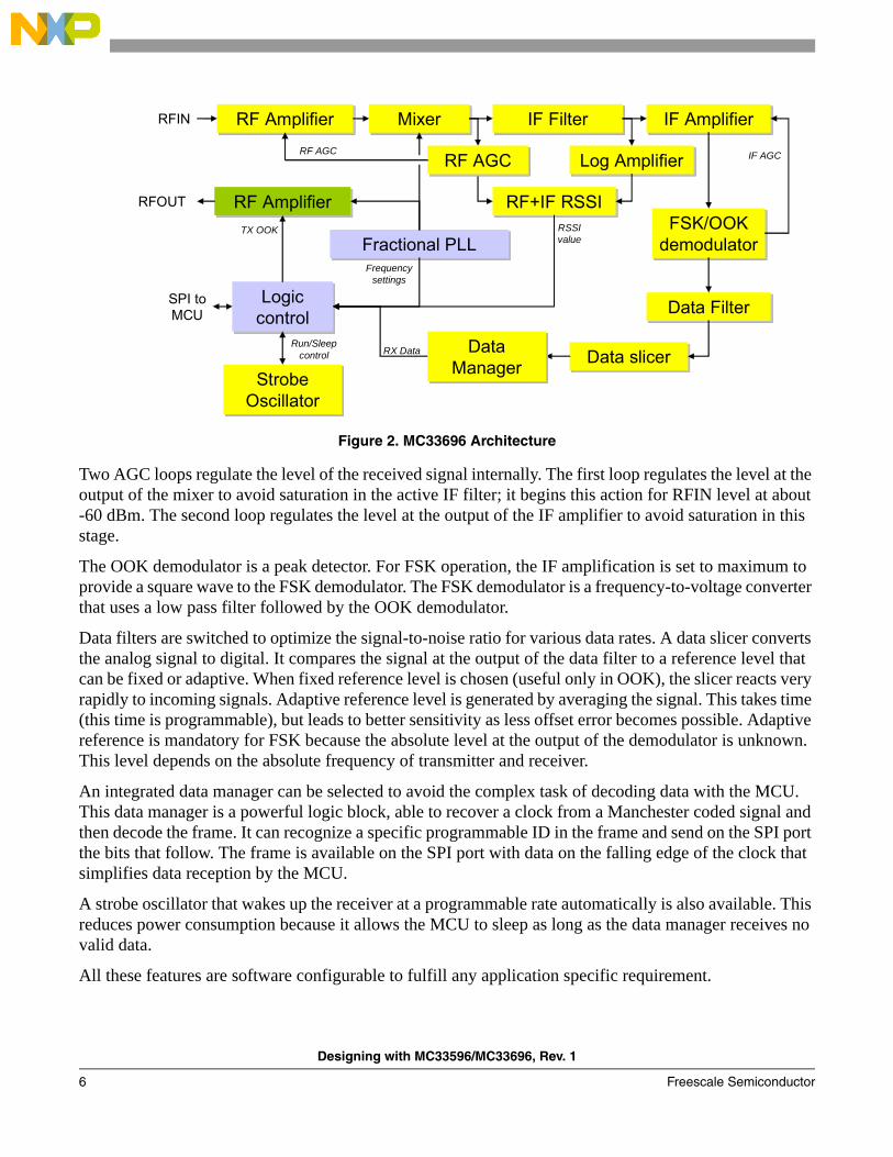
Figure 2. MC33696 Architecture
Two AGC loops regulate the level of the received signal internally. The first loop regulates the level at the output of the mixer to avoid saturation in the active IF filter; it begins this action for RFIN level at about -60 dBm. The second loop regulates the level at the output of the IF amplifier to avoid saturation in this stage.
The OOK demodulator is a peak detector. For FSK operation, the IF amplification is set to maximum to provide a square wave to the FSK demodulator. The FSK demodulator is a frequency-to-voltage converter that uses a low pass filter followed by the OOK demodulator.
Data filters are switched to optimize the signal-to-noise ratio for various data rates. A data slicer converts the analog signal to digital. It compares the signal at the output of the data filter to a reference level that can be fixed or adaptive. When fixed reference level is chosen (useful only in OOK), the slicer reacts very rapidly to incoming signals. Adaptive reference level is generated by averaging the signal. This takes time (this time is programmable), but leads to better sensitivity as less offset error becomes possible. Adaptive reference is mandatory for FSK because the absolute level at the output of the demodulator is unknown. This level depends on the absolute frequency of transmitter and receiver.
An integrated data manager can be selected to avoid the complex task of decoding data with the MCU. This data manager is a powerful logic block, able to recover a clock from a Manchester coded signal and then decode the frame. It can recognize a specific programmable ID in the frame and send on the SPI port the bits that follow. The frame is available on the SPI port with data on the falling edge of the clock that simplifies data reception by the MCU.
A strobe oscillator that wakes up the receiver at a programmable rate automatically is also available. This reduces power consumption because it allows the MCU to sleep as long as the data manager receives no valid data.
All these features are software configurable to fulfill any application specific requirement.
IF FilterIF Filter
Fractional PLLFractional PLL
RF AmplifierRF Amplifier MixerMixer IF AmplifierIF Amplifier
FSK/OOKdemodulatorFSK/OOK
demodulator
Data FilterData Filter
Data slicerData slicerStrobe
OscillatorStrobe
Oscillator
IF AGC
SPI toMCU
RF AmplifierRF Amplifier
LogiccontrolLogic
control
RF+IF RSSIRF+IF RSSI
Frequencysettings
TX OOK
RX Data
Log AmplifierLog AmplifierRF AGC
RSSIvalue
Run/Sleepcontrol
RFIN
RFOUT
Data Manager
Data Manager
RF AGCRF AGC
Designing with MC33596/MC33696, Rev. 1
Freescale Semiconductor 7
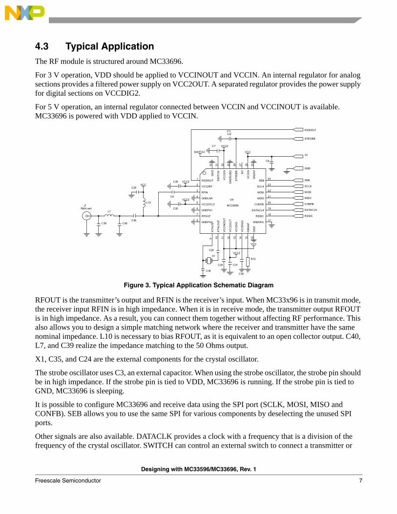
4.3 Typical ApplicationThe RF module is structured around MC33696.
For 3 V operation, VDD should be applied to VCCINOUT and VCCIN. An internal regulator for analog sections provides a filtered power supply on VCC2OUT. A separated regulator provides the power supply for digital sections on VCCDIG2.
For 5 V operation, an internal regulator connected between VCCIN and VCCINOUT is available. MC33696 is powered with VDD applied to VCCIN.
Figure 3. Typical Application Schematic Diagram
RFOUT is the transmitter’s output and RFIN is the receiver’s input. When MC33x96 is in transmit mode, the receiver input RFIN is in high impedance. When it is in receive mode, the transmitter output RFOUT is in high impedance. As a result, you can connect them together without affecting RF performance. This also allows you to design a simple matching network where the receiver and transmitter have the same nominal impedance. L10 is necessary to bias RFOUT, as it is equivalent to an open collector output. C40, L7, and C39 realize the impedance matching to the 50 Ohms output.
X1, C35, and C24 are the external components for the crystal oscillator.
The strobe oscillator uses C3, an external capacitor. When using the strobe oscillator, the strobe pin should be in high impedance. If the strobe pin is tied to VDD, MC33696 is running. If the strobe pin is tied to GND, MC33696 is sleeping.
It is possible to configure MC33696 and receive data using the SPI port (SCLK, MOSI, MISO and CONFB). SEB allows you to use the same SPI for various components by deselecting the unused SPI ports.
Other signals are also available. DATACLK provides a clock with a frequency that is a division of the frequency of the crystal oscillator. SWITCH can control an external switch to connect a transmitter or
VCC
VCC
VCC
VCC2
VCC2
SWITCH
VCC2
VCC2
C8
L7
C36
C22
C39
C7
U6
MC33696
1
2
3
4
5
69 10 11 12 13 14 16
17
18
19
20
21
22
23
24
7
8
15
2526272829303132
RSSIOUT
VCC2RF
RFIN
GNDLNA
VCC2VCO
GNDPA1X
TALI
N
XT
ALO
UT
VC
CIN
OU
T
VC
C2O
UT
VC
CD
IG
VC
CD
IG2
GN
D
GNDDIG
RSSIC
DATACLK
CONFB
MISO
MOSI
SCLK
SEB
RFOUT
GNDPA2
RB
GA
P
GN
DIO
VC
CIN
NC
ST
RO
BE
GN
DS
UB
D
VC
C2I
N
SW
ITC
H
GN
D
L10
C31
C30
X1
C31nF
C40
J1SMA vert
C35
C20
C29
C28
R13
C6
C24
SEB
MOSI
CONFB
STROBE
SCLK
GND
RSSIOUT
DATACLK
MISO
RSSIC
3V

Designing with MC33596/MC33696, Rev. 1
8 Freescale Semiconductor
receiver to the matching network. RSSIC controls the state of the RSSI circuit, allowing sampling of the incoming signal RF signal. RSSIOUT is an analog output that provides a voltage that increases with input power.
This schematic is used for the evaluation version of MC33696 RF Module. This simple design is cost effective and requires little power.
However, it does have the following drawbacks:• Adding a SAW filter to increase EMC performances of the receiver is not recommended because
RFIN and RFOUT are connected. SAW in the receiver path causes attenuation on the transmitter path as its impedance is not high when in transmit mode.
• Adding an LNA for the receiver to increase sensitivity or a PA for the transmitter to increase output power is also difficult.
The reference design version of MC33696 RF module should overcome those drawbacks.
5 MC33696 RF Module: Reference Design Version
5.1 Target of this DesignFor high performance applications requiring long range transmission with a high level of EMC performance, you may need additional filtering and amplification. Transmission output power can be increased by an additional power amplifier. EMC performance can be improved using a SAW filter that removes all high level out-of-band interferences causing intermodulation distortion or compression. An LNA is then necessary to compensate SAW filter attenuation and to prevent sensitivity loss.
After you do this, you cannot connect the receiver and transmitter path together because they cause attenuation. You must use a switch to disconnect the unused path.
Figure 4. RF Module Architecture
MC33696 can provide the signal to control the state of the switch.
MC33696MC33696
LNALNASAWSAW
Pin diodeswitch
Pin diodeswitch
PAPA
RFIN
RFOUT
Switchcontrol SWITCHTo antenna
Designing with MC33596/MC33696, Rev. 1
Freescale Semiconductor 9
5.2 Reference Design Version of the MC33696 RF Module
5.2.1 PIN Diode Switch
The pin diode switch connects the transmitter or the receiver path to the antenna.
This switch’s specifications include:• Minimum insertion loss for transmit and receive path• High isolation between transmit and receive path• Minimum current consumption when transmitting• No current consumption when receiving• Low harmonic distortion for the transmit path• Low intermodulation distortion for the receive path• Fast switching time
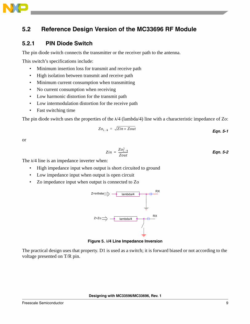
The pin diode switch uses the properties of the λ/4 (lambda/4) line with a characteristic impedance of Zo:
Eqn. 5-1
or
Eqn. 5-2
The λ/4 line is an impedance inverter when:• High impedance input when output is short circuited to ground• Low impedance input when output is open circuit• Zo impedance input when output is connected to Zo
Figure 5. λ/4 Line Impedance Inversion
The practical design uses that property. D1 is used as a switch; it is forward biased or not according to the voltage presented on T/R pin.
Zoλ 4⁄ Zin Zout×=
ZinZoλ 4⁄
2
Zout--------------=
Z=infiniteRX
lambda/4
RXlambda/4Z=Zo
Designing with MC33596/MC33696, Rev. 1
10 Freescale Semiconductor
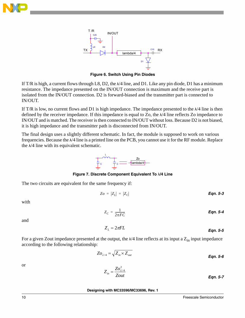
Figure 6. Switch Using Pin Diodes
If T/R is high, a current flows through L8, D2, the λ/4 line, and D1. Like any pin diode, D1 has a minimum resistance. The impedance presented on the IN/OUT connection is maximum and the receive part is isolated from the IN/OUT connection. D2 is forward-biased and the transmitter part is connected to IN/OUT.
If T/R is low, no current flows and D1 is high impedance. The impedance presented to the λ/4 line is then defined by the receiver impedance. If this impedance is equal to Zo, the λ/4 line reflects Zo impedance to IN/OUT and is matched. The receiver is then connected to IN/OUT without loss. Because D2 is not biased, it is high impedance and the transmitter path is disconnected from IN/OUT.
The final design uses a slightly different schematic. In fact, the module is supposed to work on various frequencies. Because the λ/4 line is a printed line on the PCB, you cannot use it for the RF module. Replace the λ/4 line with its equivalent schematic.
Figure 7. Discrete Component Equivalent To λ/4 Line
The two circuits are equivalent for the same frequency if:
Eqn. 5-3
with
Eqn. 5-4
and
Eqn. 5-5
For a given Zout impedance presented at the output, the λ/4 line reflects at its input a Zin input impedance according to the following relationship:
Eqn. 5-6
or
Eqn. 5-7
C10
D1
L8 D2
C25
lambda/4RXTX
IN/OUTT /R
L
CC lambda/4Zo
Zo ZL ZC= =
ZC1
2πFC---------------=
FLZL π2=
outin ZZZo ×=4/λ
ZoutZoZin
24/λ=

Designing with MC33596/MC33696, Rev. 1
Freescale Semiconductor 11
By changing L and C, you can optimize Zo and Zin to minimize the loss due to the connection of the receiver path when MC33696 is transmitting.
Diodes used for D1 and D2 are HSMP-3890 from Agilent. They have low impedance even if biased with low current. They also offer very low harmonic distortion for transmitter and do not degrade the overall intermodulation distortion for the receiver.
As D1 can have an ON impedance of about 8Ω when forward biased, it is necessary to have a high Zo value to obtain a high Zin for proper insulation when transmitting.
The initial design choice for the characteristic impedance of the λ/4 line was 50Ω Zo impedance. Then, by short circuiting C14 (Zout=0), Zin impedance can be evaluated because it is also dependant on the Q factor of the various components (or losses). The final choice for Zo is about 300Ω. An additional matching network between C10 and the SAW filter used is required. Exact impedance for the λ/4 line is not critical.
Figure 8. Practical Implementation of the λ/4 Switch
C9 compensates the inductive part of D1 and associated components that kill the high Zin wanted. By tuning C9, you can have a high pure resistive Zin at the input port.
If T/R equals 1, the switch is in transmit mode:• Q2 is ON and bypass C21• D2 is forward bias and connect TX to the IN/OUT port• D1 is biased with R6 and presents a low Zout impedance to the λ/4 line output• The λ/4 line presents a high impedance to the IN/OUT port • RX path is then disconnected
If T/R equals 0, the switch is in receive mode:• Q2 is OFF• D2 is not biased and TX is isolated from the IN/OUT port• D1 is not biased and presents an high impedance to the RX port• RX is connected to the IN/OUT port through the λ/4 line
VCC
.
D2HSMP-3890
C101nF
C251nF
D1HSMP-3890
L8100nH
C131.2pF
C141.2pF
L347nH
Q2BSS138 R9
1M
C214.7nF
R61.5k
C96.8pF RX
IN/OUT
TX
T /R
Designing with MC33596/MC33696, Rev. 1
12 Freescale Semiconductor
The performances of the switch (with matching network to 50 Ω on all ports) are:• current consumption: 1 mA for 3 V in TX mode• TX attenuation: −0.8 dB• RX attenuation: −1 dB• Isolation TX-RX: 24 dB
5.2.2 Low Noise Amplifier
The low noise amplifier (LNA) should compensate for the losses of the SAW filter. It should improve overall performance and not degrade high level behavior of the receiver.
Specifications for the LNA include:• Low noise figure• +10 dB power gain• 1 mA current consumption• High IP3• Current consumption that can be switched to 0 mA when not receiving• SOT23 package, low cost
Some of those specifications are in opposition. High IP3 and high power gain may require a high current. Some compromises must be made. The LNA’s design should be optimal for a given current consumption.
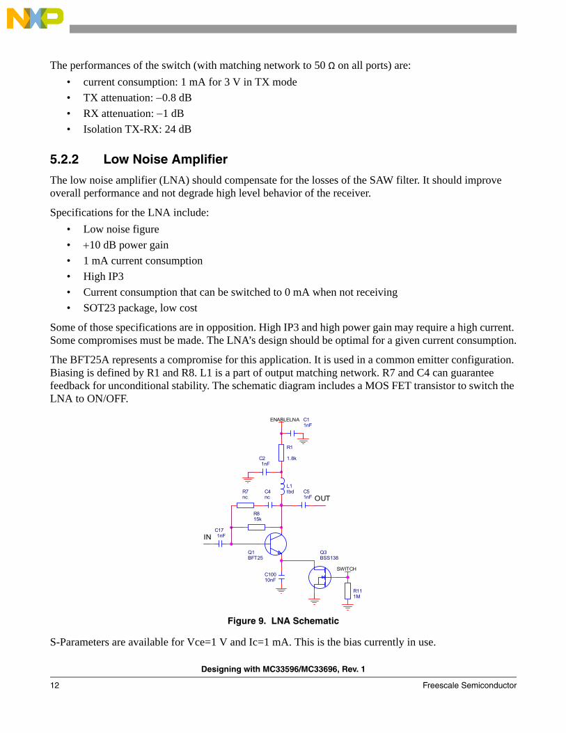
The BFT25A represents a compromise for this application. It is used in a common emitter configuration. Biasing is defined by R1 and R8. L1 is a part of output matching network. R7 and C4 can guarantee feedback for unconditional stability. The schematic diagram includes a MOS FET transistor to switch the LNA to ON/OFF.
Figure 9. LNA Schematic
S-Parameters are available for Vce=1 V and Ic=1 mA. This is the bias currently in use.
SWITCH
ENABLELNA
C10010nF
L1tbd
C21nF
C171nF
C11nF
R815k
R7nc
Q1BFT25
C4nc
R111M
R1
1.8k
Q3BSS138
C51nF OUT
IN

Designing with MC33596/MC33696, Rev. 1
Freescale Semiconductor 13
5.2.2.1 Design Using S-Parameters
You can design an LNA using S-Parameters. If the LNA is unconditionally stable, you can define the maximum power gain and the terminal impedances to obtain stability and amplification. If the device chosen is not unconditionally stable at any frequency, a feedback can be applied to modify the LNA S-Parameters.
For the study of this LNA, an Excel sheet has been created to evaluate over a wide frequency band:• The stability criteria (to know if a device is unconditionally stable or not)• The maximum available gain• The conjugate match impedances (impedance to present to have maximum gain)• The impedance to present for a given gain• The location and radius of the stability circles (location on the Smith chart of the impedances to
present to have stability)• The location and radius of the NF circles (location on the Smith chart of the impedances to present
to have a given noise factor)• The resulting S-parameters for a device with an RLC feedback
This Excel sheet gives the computations using the transistor S-Parameters:
Figure 10. S-Parameters Matrix
5.2.2.1.1 Stability
Rollet stability factor (K) computation shows a device is unconditionally stable or not:
Eqn. 5-8
with
Eqn. 5-9
If K is greater than 1, the device is unconditionally stable. It is stable for any combination of source and load impedances.
If K is less than 1, the transistor is conditionally stable for some combinations of source and load impedances. In this case, choose another transistor for your application, another bias point, or compute the source and load impedances that can be used in a stable configuration.
⎥⎦
⎤⎢⎣
⎡=
2221
1211
SSSS
S
1221
222
211
2
21
SSSSDs
K××
−−+=
21122211 SSSSDs ×−×=

Designing with MC33596/MC33696, Rev. 1
14 Freescale Semiconductor
5.2.2.1.2 Maximum Available Gain (MAG)
The MAG is the maximum available gain that can be obtained from a device if its input and output reflection coefficients fulfill some conditions (See Section 5.2.2.1.3, “Simultaneous Conjugate Match”).
Eqn. 5-10
with:
Eqn. 5-11
Eqn. 5-12
K is the Rollet Stability Factor
NOTEThe MAG is defined only for unconditional stable transistors because K has to be greater than 1.
5.2.2.1.3 Simultaneous Conjugate Match
The MAG is obtained by applying the impedances representing the conjugate matching that matches input and output to the device ports.
The output load coefficient is defined by:
Module:
Eqn. 5-13
Argument:
Eqn. 5-14
with
Eqn. 5-15
Eqn. 5-16
Eqn. 5-17
( )1²)(log10log10 112
21−×+×+×= KBsignofK
SS
MAGdB
²²²1 22111 DsSSB −−+=
21122211 SSSSDs ×−×=
( )( )2
2222
2²4²
CCBBsignofB
L×
×−×−=Γ
2CL −∠=Γ∠
²²²1 11222 DsSSB −−+=
21122211 SSSSDs ×−×=
( )*11222 SDsSC −=
Designing with MC33596/MC33696, Rev. 1
Freescale Semiconductor 15
The input load coefficient is defined by:
Eqn. 5-18
5.2.2.1.4 Practical Design
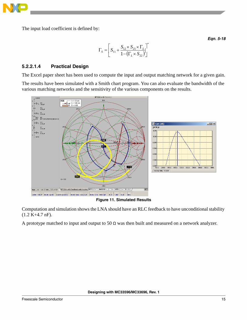
The Excel paper sheet has been used to compute the input and output matching network for a given gain.
The results have been simulated with a Smith chart program. You can also evaluate the bandwidth of the various matching networks and the sensitivity of the various components on the results.
Figure 11. Simulated Results
Computation and simulation shows the LNA should have an RLC feedback to have unconditional stability (1.2 K+4.7 nF).
A prototype matched to input and output to 50 Ω was then built and measured on a network analyzer.
( )
*
22
211211 1 ⎥
⎦
⎤⎢⎣
⎡×Γ−
Γ××+=Γ
SSSSL
LS

Designing with MC33596/MC33696, Rev. 1
16 Freescale Semiconductor
Figure 12. LNA Prototype
This prototype showed the following performances: • 9.9 dB gain (for 11.57 dB by simulation)• 1 mA current consumption• NF not measured
Later, the LNA on the final PCB presented different characteristics as tracks and ground connections of emitter changes the LNA S-parameters. As a result, RLC feedback was no longer needed.
5.2.3 Power Amplifier
The power amplifier (PA) should increase the output power of the transmitter with minimum current consumption and distortion.
We can define some specifications for the PA:• +5 dB to +10 dB gain• +10 dBm output power• Less than 15 mA current consumption• Low distortion• Current consumption may be switched to 0 mA when not transmitting• SOT23 package, low cost
The BFR520 is indicated for this kind of application. To minimize distortion, a feedback network is used.
ENABLELNA
L5
L2
C11
C19C18
C12J1
J2
C11nF
C21nF
C171nF
L1tbd
R815k
C44.7nF
R71.2k
Q1BFT25
R1
1.8k
C51nF

Designing with MC33596/MC33696, Rev. 1
Freescale Semiconductor 17
Figure 13. PA Prototype
The design of a PA cannot be used with low-level parameters like S-Parameters. You may need to use hot S-Parameters (S-Parameter characterization using high level signals) or deal with an intensive RF simulation or lab test.
One prototype that provides +8.8 dBm for 15 mA power consumption and reasonable distortion exists.
But because the latest version of MC33696 silicon provides about +7 dBm at low frequency, demand for an external PA is too low to justify the additional current consumption.
Even with some provisions for the PA on the printed circuit board, it is not equipped with components.
ENABLEPAVCC
C37
C34
C27
C38
C26
Q4BFR520 C41
L9R15
C33 R14
C42
L6
L11 IN
OUT

Designing with MC33596/MC33696, Rev. 1
18 Freescale Semiconductor
5.2.4 Schematic Diagram of MC33696/MC33596 RF Module
The schematics presented here show only the 433.92 MHz versions. For information on other frequencies, see Section 11, “Bill of Material.”
5.2.4.1 MC33696 Reference Design at 433.92MHz
Figure 5-13 shows the version developed in this application note. MC33696 is surrounded by an LNA, a SAW filter, and a PIN diode Switch. This version is not available as an evaluation tool.
Figure 14. MC33696 Reference Design Schematic Diagram
ENABLELNA
SWITCH
VCC
SWITCH
VCC2
VCC2
ENABLEPA
VCC
ENABLELNA
VCC
VCC
VCC2
VCC2
R100
L722nH
TP1VCCIO
L8100nH
L1100nH
C7100pF
L347nH
C21nF
C1011.8pF
C31100nF
C22100pF
C30100nF
C171nF
C11nF
D2HSMP-3890
R815k
C96.8pF
L10122nH
R61.5k
C1028.2pF
J1-11
J1-33C8100nF
J1-2525
J1-1919J1-1717J1-2121
X124.19066MHz
J1-1313
J1-3131
J1-2929
J1-3333
J1-2727
J1-3535
J1-1818
J1-2323
Q1BFT25
R50R
C152.7pF
L10027nH
R11.8k
C101nF
C3247pF
C31nF
C378.2pF
R1210k
J2SMA v ert
C251nF
L247nH
L927nH
C141.2pF
C131.2pF
C29100nF
C122.2pF
D1HSMP-3890
C356.8pF
R9nc
C214.7nF
C61nF
C20100nF
C51nF
F1RF1172B
1
2
3
4
5
6
7
8
C113.3pF
R170
R13470k 1%
Q2BSS138
C241nF
J1-1515
R1020
U4
MC33696
1
2
3
4
5
6
9 10 11 12 13 14 16
17
18
19
20
21
22
23
24
7
8
15
2526272829303132
RSSIOUT
VCC2RF
RFIN
GNDLNA
VCC2VCO
GNDPA1
XTA
LIN
XTA
LOU
T
VC
CIN
OU
T
VCC
2OU
T
VC
CD
IG
VCC
DIG
2
GN
D
GNDDIG
RSSIC
DATACLK
CONFB
MISO
MOSI
SCLK
SEB
RFOUT
GNDPA2
RB
GAP
GN
DIO
VC
CINNC
STR
OB
E
GN
DSU
BD
VC
C2I
N
SWIT
CH
GN
D
SEB
MOSI
CONFB
STROBE
VCC
/SS
SCLK
GND
RSSIOUT
ENABLELNA
DATACLK
MISO
RSSIC
ENABLEPA
TX DATA
C396.8pF
C404.7pF
Designing with MC33596/MC33696, Rev. 1
Freescale Semiconductor 19
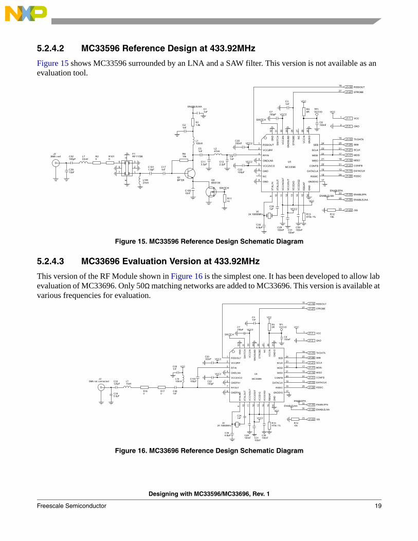
5.2.4.2 MC33596 Reference Design at 433.92MHz
Figure 15 shows MC33596 surrounded by an LNA and a SAW filter. This version is not available as an evaluation tool.
Figure 15. MC33596 Reference Design Schematic Diagram
5.2.4.3 MC33696 Evaluation Version at 433.92MHz
This version of the RF Module shown in Figure 16 is the simplest one. It has been developed to allow lab evaluation of MC33696. Only 50Ω matching networks are added to MC33696. This version is available at various frequencies for evaluation.
Figure 16. MC33696 Reference Design Schematic Diagram
SWITCH
ENABLEPA
VCC
VCC
VCC
VCC2
SWITCH
ENABLELNA
ENABLELNA
VCC2
VCC2
VCC2
R13470k 1%
C241nF
J1-1515
U5
MC33596
1
2
3
4
5
6
9 10 11 12 13 14 16
17
18
19
20
21
22
23
24
7
8
15
2526272829303132
RSSIOUT
VCC2RF
RFIN
GNDLNA
VCC2VCO
GND
XTAL
IN
XTA
LOU
T
VCC
INO
UT
VCC
2OU
T
VCC
DIG
VC
CD
IG2
GN
D
GNDDIG
RSSIC
DATACLK
CONFB
MISO
MOSI
SCLK
SEB
NC
GND
RBG
AP
GN
DIO
VC
CINNC
STR
OBE
GN
DSU
BD
VCC
2IN
SW
ITC
H
GN
D
TP1VCCIO
L722nH
C3912pF
L1100nH
C7100pF
C21nF
C22100pF
C31100nF
C1011.8pF
C11nF
C30100nF
C171nF
R815k
R11nc
R20
C8100nF J1-33
J1-11
J1-1919
J1-2525
J1-2121
J1-1717
X124.19066MHz
J1-2929
J1-3131
J1-1313
J1-1818
J1-3535
J1-2727
J1-3333
J1-2323
C10010nF
R1010
Q1BFT25
R50R
L10027nH
R11.8k
C31nF
C32100pF
R1210k
Q3BSS138
J2SMA v ert
L247nH
C29100nF
C122.2pF
C356.8pF
C20100nF
C51nF
C61nF
F1RF1172B
1
2
3
4
5
6
7
8
C113.3pF
SEB
MOSI
CONFB
STROBE
VCC
/SS
SCLK
GND
RSSIOUT
ENABLELNA
DATACLK
MISO
RSSIC
ENABLEPA
TX DATA
VCC
SWITCH
VCC2
VCC2
ENABLEPA
VCC
ENABLELNA
VCC
VCC2
VCC2
TP1VCCIO
J1-1515
C7100pF
C241nF
C8100nF
C31100nF
C30100nF
J1-2121
J1-1717
J1-33
J1-11
J1-1919
J1-1313
J1-2525
J1-3333
X124.19066MHz
J1-3131
J1-2929
J1-2323
J1-1818
J1-2727
R50R
J1-3535
U4
MC33696
1
2
3
4
5
6
9 10 11 12 13 14 16
17
18
19
20
21
22
23
24
7
8
15
2526272829303132
RSSIOUT
VCC2RF
RFIN
GNDLNA
VCC2VCO
GNDPA1
XT
ALI
N
XT
ALO
UT
VC
CIN
OU
T
VC
C2O
UT
VC
CD
IG
VC
CD
IG2
GN
D
GNDDIG
RSSIC
DATACLK
CONFB
MISO
MOSI
SCLK
SEB
RFOUT
GNDPA2
RB
GA
P
GN
DIO
VC
CINNC
ST
RO
BE
GN
DS
UB
D
VC
C2I
N
SW
ITC
H
GN
D
C356.8pF
R1210k
C31nF
R13470k 1%
C29100nF
C20100nF
C22100pF
C103100pF
SEB
MOSI
CONFB
STROBE
VCC
/SS
SCLK
GND
RSSIOUT
ENABLELNA
DATACLK
MISO
RSSIC
ENABLEPA
TX DATA
C361nF
L715nH
C395.6pF
L10100nH
R160
C32120pF
J2SMA not connected
R170
VCCC281nF

Designing with MC33596/MC33696, Rev. 1
20 Freescale Semiconductor
5.2.4.4 Schematic Diagram Common to MC33696/MC33596 RF Modules Versions
The schematic shown in Figure 17 is used to allow the CAD generation of different versions of MC33696 RF Modules. It is possible to obtain various schematics by adding or removing components:
• MC33696 Evaluation Version:— MC33696— 50Ω Matching network
• MC33696 Reference Design Version:— MC33696— LNA— SAW Filter— Power Amplifier (not developed)— Pin Diode Switch— 50Ω Matching network
Figure 17. Complete Schematic Diagram Used for CAD Design
SWITCH
VCC
ENABLELNA
SWITCH
ENABLEPA
SWITCH
VCC2
VCC2
VCC
VCCVCC
VCC2
VCC2 U2
MC33696
1
2
3
4
5
6
9 10 11 12 13 14 16
17
18
19
20
21
22
23
24
7
8
15
2526272829303132
RSSIOUT
VCC2RF
RFIN
GNDLNA
VCC2VCO
GNDPA1
XTAL
IN
XTAL
OU
T
VCCI
NO
UT
VCC2
OUT
VCC
DIG
VCCD
IG2
GN
D
GNDDIG
RSSIC
DATACLK
CONFB
MISO
MOSI
SCLK
SEB
RFOUT
GNDPA2
RBG
AP
GN
DIO
VCC
INNC
STRO
BE
GN
DSU
BD
VCC2
IN
SWIT
CHGN
D
C22100pF
C31100nF
C2tbd
L3tbd
C17tbd
C30100nF
D2
HSMP-3890
C33tbd
L4tbd R8
tbd
C41tbd
C1tbd
R6tbd
R20
L10tbd
C9tbd
C38tbd
C16tbd
C34tbd
Q4BFR520
X1NX5032GA
Q1BFT25
R7tbd
R50R
C15tbd
C4tbd
R160
R150
C10tbd
R1
tbd
R11tbd
L5tbd
C37tbd
C31nF
R14tbd
C32tbd
R30
Q3BSS138
C25tbd
C27tbd
L2tbd
J2SMA vert
R1000
R40
C40tbd
C13tbd
L9tbd
C12tbd
C29100nF
C28tbd
C14tbd
D1HSMP-3890
C358pF
C21tbd
C26tbd
C5tbd
C6tbd
R9tbd
C20100nF
C11tbd
F1RF1172B
1
2
3
4
5
6
7
8
R13470k 1%
L11tbd
C241nF
Q2BSS138
R170
C19tbd
L8tbd
L7tbd
L1tbd
C39tbd
R100R
L6tbd
C36tbd
C7100pF
C18tbd
C42tbd
SAWFILTER
LOW NOISEAMPLIFIER
50 OHMSMATCHINGNETWORK
ECHO TXBIAS
PIN DIODESWITCH
POWERAMPLIFIER
VCC
ENABLEPA
VCC
ENABLELNA
J1-11
C8100nF
J1-2525
J1-2121
J1-33
J1-1717
J1-1919
J1-2929
J1-3131
J1-2727
J1-1313
J1-1818
J1-3535J1-3333
J1-2323
R1210k
J1-1515
TP1VCCIO
SEB
MOSI
CONFB
STROBE
VCC
/SS
SCLK
GND
RSSIOUT
ENABLELNA
DATACLK
MISO
RSSIC
ENABLEPA
TX DATA

Designing with MC33596/MC33696, Rev. 1
Freescale Semiconductor 21
6 Connector Pin OutAll the logic level signals available on J1 are referred to as VDD and GND. Do not apply any signal higher than VDD or lower than GND to the module.
Figure 18. Connector Pin Out
Table 2.
Number Name Type Function
1 VDD Power supply 3 V for MC33696 and LNA.
3 GND Power supply To be connected to a large ground plane
13 DATACLK Output Clock for MCU timer
15 DATA Input Transmitter input
17 MOSI Input/Output Serial data for the SPI port
18 RSSIOUT Output Analog RSSI output
19 MISO Output Serial data for the SPI port
21 SCLK Input/Output Serial clock for the SPI port
25 SEB Input Serial Bus Enable. Connect to 1 to enable SPI bus
27 STROBE Input Strobe oscillator control0: strobe oscillator is stopped and MC33696 sleeps1: strobe oscillator is stopped and MC33696 runshigh: strobe oscillator is running
31
27
7
13
29
35
1917
1
21
15
33
2325
3
9
5
11
3634
8
22
26
6
24
20
32
181614
2
30
4
28
1210
GND
DATACLK
MISOSCLK
VCC
SEBSTROBE
RSSICCONFB
RSSIOUT
/SS
ENABLEPA
MOSITX DATA
ENABLELNA

Designing with MC33596/MC33696, Rev. 1
22 Freescale Semiconductor
7 First Step For Receiver TestingThe following set-up allows measurement of the sensitivity of MC33696's receiver:
• 433.92 MHz• 4800 bps• No data manager• OOK or FSK
To test the receiver in other configurations, refer to the registers description in the MC33696 datasheet to modify the settings properly.
For other frequencies, additional script files are provided in the CD attached to the MC33696 RF Module.
7.1 Test Set Up for OOK and FSK• Plug the RF module into the MCU board• Connect the MCU board to the PC with an RS232 cable• Connect an RF generator to the SMA connector
— OOK configuration:– Frequency: 433.92 MHz– Modulation: pulse (or 100% AM square wave), 4.8 kHz– RF level: -70 dBm
— FSK configuration: – Frequency: 433.92 MHz– Modulation: FSK ±50 kHz, 4.8 kHz– RF level: −70 dBm
• Connect an oscilloscope probe on MOSI (pin 17 of connector)— 1 V/div, 20 µs/div
29 RSSIC Input RSSI control0: RSSI sampled on falling edge1: RSSI continuously updated
31 CONFB Input Configuration mode/normal mode control for the SPI port
33 ENABLEPA Input PA bias control0: PA is OFF1: PA is ON. Normal mode during transmission
35 ENEBLELNA Input LNA bias control0: LNA is OFF.1: LNA is ON. Normal mode during reception
Table 2.
Number Name Type Function

Designing with MC33596/MC33696, Rev. 1
Freescale Semiconductor 23
• Connect a voltmeter or a oscilloscope probe on RSSIOUT (pin 17 of connector)• Apply 9 V power supply to the MCU board
7.2 Registers and Pins Set upUse scripts to avoid manual setting (see files in RF modules kit CD ROM). Use the control software to set up registers and pins as given in the following sections.
7.2.1 RX OOK 433.92 MHz• STROBE 1• SEB 0• CONFIG1 50• CONFIG2 cD• CONFIG3 00• COMMAND 19• F 07F5• FT 7096F7• ID 00• HEADER 00• DATA Z• PA 0• LNA 1• RSSIC 1
7.2.2 RX FSK 433.92 MHz• STROBE 1• SEB 0• CONFIG1 50• CONFIG2 ED• CONFIG3 00• COMMAND 19• F 07F5• FT 7096F7• ID 00• HEADER 00• DATA Z• PA 0• LNA 1

Designing with MC33596/MC33696, Rev. 1
24 Freescale Semiconductor
• RSSIC 1
7.2.3 Measurements
The oscilloscope shows the demodulated signal. Decrease RF signal levels and control the quality of the demodulated signal to evaluate sensitivity.
The voltmeter measures RSSI analog voltage. Change the RF signal level to check influence.
8 First Step for Transmitter TestingThe following set up allows you to measure the output power and spectral purity of MC33696's transmitter:
• 433.92 MHz• Continuous wave or modulated• OOK or FSK
To test the transmitter in other configurations, refer to the registers description in MC33696 datasheet to modify settings properly.
For other frequencies, additional script files are provided in CD attached to the MC33696 RF Module.
8.1 Test Set-Up• Plug the RF module onto the MCU board• Connect the MCU board to the PC with an RS232 cable• Connect a spectrum analyzer to the SMA connector
– Center frequency: 433.92 MHz– Span: 1 MHz– Reference level: 15 dBm– RBW: auto or 10 kHz
• Apply 9 V power supply to the MCU board
8.2 Registers and Pins Set UpUse scripts to avoid manual setting (see files in RF Modules kit CD ROM). Use the control software to set up registers and pins as given in the following sections.

Designing with MC33596/MC33696, Rev. 1
Freescale Semiconductor 25
8.2.1 TX OOK 433.92 MHz• CONFB 1• STROBE 1• SEB 0• CONFIG1 50• CONFIG2 CD• CONFIG3 00• COMMAND 39• F 07F5• FT 7006F7• DATA 1• PA 1• LNA 0• RSSIC 0
8.2.2 TX FSK 433.92 MHz• CONFB 1• STROBE 1• SEB 0• CONFIG1 50• CONFIG2 ED• CONFIG3 00• COMMAND 39• F 07F5• FT 7086F7• DATA 1• PA 1• LNA 0• RSSIC 0

Designing with MC33596/MC33696, Rev. 1
26 Freescale Semiconductor
8.3 MeasurementsThe spectrum analyzer displays the RF spectrum and allows peak power measurement.
To make measurements using modulated waves, use the following command:• TXSQUARE 208
This modulates the signal with a square wave at 4800 bps or 208 µs period.
Stop modulation by striking the return key.
To allow another transmission in CW mode:• MODE 1• DATA 1
9 MC33696/MC33596 RF Module Performances
9.1 Performance VariablesTable 3 shows measurements done with the conditions:
• RX: OOK 4.8 kbps, sensitivity measured for BER = 10−3• TX: continuous wave, peak power measurement
Table 3. Measurements
Ref Frequency RX Sensitivity TX Power RX current TX current
MC33696MOD315EV 315 MHz −105 dBm +8 dBm 8.8 mA 12 mA
MC33696MOD434EV 433.92 MHz −104 dBm +7.5 dBm 9 mA 13 mA
MC33696MOD868EV 868.3 MHz −103 dBm +4 dBm 9.2 mA 13 mA
MC33696MOD916EV 916.5 MHz −103 dBm +3.5 dBm 9 mA 12.5 mA
MC33696MOD434 433.92 MHz −106 dBm +7 dBm 10.2 mA 13.5 mA
MC33596MOD434 433.92 MHz −106 dBm na 10.2 mA na

Designing with MC33596/MC33696, Rev. 1
Freescale Semiconductor 27
10 PCB Design
10.1 LayoutBe careful with the layout of the PCB by using a double-sided PCB.
MC33696/MC33596:• Use a large ground plane on the opposite layer• Connect each ground pin to the ground plane using a separate via for each signal. Do not use a
common via• Place each decoupling capacitor as close as possible (no more than 2-3 mm) to the corresponding
VDD pin• VCCDIG2 decoupling capacitor (C30) should be placed directly between VCCDIG2 (pin 14) and
GND (pin 16)• Crystal X1 and associated capacitors C24 and C36 should be close to U1. Avoid loops due to the
component size and tracks. Avoid digital signal routing in this area.
SAW filter:• Connect each ground return directly to the ground plane. Avoid common via to guarantee
maximum out of band rejection• The associated matching network should have separate ground connections
LNA:• The connection of the Q1 emitter should be very short to ground to minimize track inductance and
maintain stability• Feedback components (R5, R6, C4) should be connected directly between base and collector• The C2 decoupling capacitor should be connected directly between L1 and ground
Other:• Minimize any track routing RF signal• Use high frequency coils with high Q values for the frequency of operation (min 15). Any change
of coil source should be validated• Avoid proximity of any input and output of a block to maintain stability (LNA) or maximum
rejection (SAW filter)• If the ground plane has to be cut on the opposite layer to route on a signal, maintain the continuity
with another ground plane on the opposite layer and a lot of via to have minimum parasitic inductance
• If you can afford a multilayer PCB, use an internal layer for the ground plane. Route the power supply and digital signals on the last layer. RF components are placed on the first layer.
NOTEMatching networks should be retuned if any change has been made to PCB (track width, length or place, PCB thickness, component value). Never use a matching network designed for another PCB.
Desig
nin
g w
ith M
C33596/M
C33696, R
ev. 1
28Freescale S
emiconductor
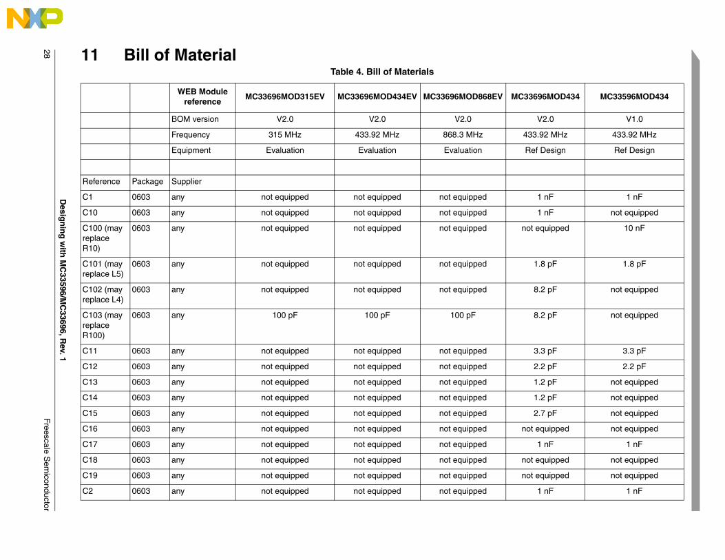
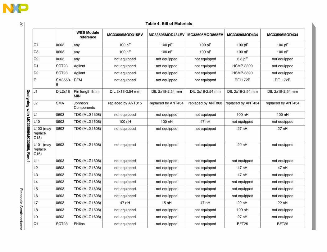
11 Bill of MaterialTable 4. Bill of Materials
WEB Module reference
MC33696MOD315EV MC33696MOD434EV MC33696MOD868EV MC33696MOD434 MC33596MOD434
BOM version V2.0 V2.0 V2.0 V2.0 V1.0
Frequency 315 MHz 433.92 MHz 868.3 MHz 433.92 MHz 433.92 MHz
Equipment Evaluation Evaluation Evaluation Ref Design Ref Design
Reference Package Supplier
C1 0603 any not equipped not equipped not equipped 1 nF 1 nF
C10 0603 any not equipped not equipped not equipped 1 nF not equipped
C100 (may replace R10)
0603 any not equipped not equipped not equipped not equipped 10 nF
C101 (may replace L5)
0603 any not equipped not equipped not equipped 1.8 pF 1.8 pF
C102 (may replace L4)
0603 any not equipped not equipped not equipped 8.2 pF not equipped
C103 (may replace R100)
0603 any 100 pF 100 pF 100 pF 8.2 pF not equipped
C11 0603 any not equipped not equipped not equipped 3.3 pF 3.3 pF
C12 0603 any not equipped not equipped not equipped 2.2 pF 2.2 pF
C13 0603 any not equipped not equipped not equipped 1.2 pF not equipped
C14 0603 any not equipped not equipped not equipped 1.2 pF not equipped
C15 0603 any not equipped not equipped not equipped 2.7 pF not equipped
C16 0603 any not equipped not equipped not equipped not equipped not equipped
C17 0603 any not equipped not equipped not equipped 1 nF 1 nF
C18 0603 any not equipped not equipped not equipped not equipped not equipped
C19 0603 any not equipped not equipped not equipped not equipped not equipped
C2 0603 any not equipped not equipped not equipped 1 nF 1 nF

Desig
nin
g w
ith M
C33596/M
C33696, R
ev. 1
Freescale Sem
iconductor29
C20 0603 any 100 nF 100 nF 100 nF 100 nF 100 nF
C21 0603 any not equipped not equipped not equipped 4.7 nF not equipped
C22 0603 any 100 pF 100 pF 100 pF 100 pF 100 pF
C24 0603 any 1 nF 1 nF 1 nF 1 nF 1 nF
C25 0603 any not equipped not equipped not equipped 1 nF not equipped
C26 0603 any not equipped not equipped not equipped not equipped not equipped
C27 0603 any not equipped not equipped not equipped not equipped not equipped
C28 0603 any 1 nF 1 nF 1 nF not equipped not equipped
C29 0603 any 1 nF 1 nF 1 nF 100 nF 1 nF
C3 0603 any 1 nF 1 nF 1 nF 1 nF 1 nF
C30 0603 any 10 nF 10 nF 10 nF 100 nF 10 nF
C31 0603 any 10 nF 10 nF 10 nF 100 nF 10 nF
C32 0603 any 82 pF 120 pF 27 pF 47 pF 100 pF
C33 0603 any not equipped not equipped not equipped not equipped not equipped
C34 0603 any not equipped not equipped not equipped not equipped not equipped
C35 0603 any 6.8 pF 6.8 pF 6.8 pF 6.8 pF 6.8 pF
C36 0603 any 1 nF 1 nF 1 nF not equipped not equipped
C37 0603 any not equipped not equipped not equipped 8.2 pF not equipped
C38 0603 any not equipped not equipped not equipped not equipped not equipped
C39 0603 any 3.9 pF 5.6 pF 0.47 pF 6.8 pF 12 pF
C4 0603 any not equipped not equipped not equipped not equipped not equipped
C40 0603 any not equipped not equipped not equipped 4.7 pF not equipped
C41 0603 any not equipped not equipped not equipped not equipped not equipped
C42 0603 any not equipped not equipped not equipped not equipped not equipped
C5 0603 any not equipped not equipped not equipped 1 nF 1 nF
C6 0603 any not equipped not equipped not equipped 1 nF 1 nF
Table 4. Bill of Materials
WEB Module reference
MC33696MOD315EV MC33696MOD434EV MC33696MOD868EV MC33696MOD434 MC33596MOD434
Desig
nin
g w
ith M
C33596/M
C33696, R
ev. 1
30Freescale S
emiconductor
C7 0603 any 100 pF 100 pF 100 pF 100 pF 100 pF
C8 0603 any 100 nF 100 nF 100 nF 100 nF 100 nF
C9 0603 any not equipped not equipped not equipped 6.8 pF not equipped
D1 SOT23 Agilent not equipped not equipped not equipped HSMP-3890 not equipped
D2 SOT23 Agilent not equipped not equipped not equipped HSMP-3890 not equipped
F1 SM8558-8
RFM not equipped not equipped not equipped RF1172B RF1172B
J1 DIL2x18 Pin length 8mm MIN
DIL 2x18-2.54 mm DIL 2x18-2.54 mm DIL 2x18-2.54 mm DIL 2x18-2.54 mm DIL 2x18-2.54 mm
J2 SMA Johnson Components
replaced by ANT315 replaced by ANT434 replaced by ANT868 replaced by ANT434 replaced by ANT434
L1 0603 TDK (MLG1608) not equipped not equipped not equipped 100 nH 100 nH
L10 0603 TDK (MLG1608) 100 nH 100 nH 47 nH not equipped not equipped
L100 (may replace C18)
0603 TDK (MLG1608) not equipped not equipped not equipped 27 nH 27 nH
L101 (may replace C16)
0603 TDK (MLG1608) not equipped not equipped not equipped 22 nH not equipped
L11 0603 TDK (MLG1608) not equipped not equipped not equipped not equipped not equipped
L2 0603 TDK (MLG1608) not equipped not equipped not equipped 47 nH 47 nH
L3 0603 TDK (MLG1608) not equipped not equipped not equipped 47 nH not equipped
L4 0603 TDK (MLG1608) not equipped not equipped not equipped not equipped not equipped
L5 0603 TDK (MLG1608) not equipped not equipped not equipped not equipped not equipped
L6 0603 TDK (MLG1608) not equipped not equipped not equipped not equipped not equipped
L7 0603 TDK (MLG1608) 47 nH 15 nH 47 nH 22 nH 22 nH
L8 0603 TDK (MLG1608) not equipped not equipped not equipped 100 nH not equipped
L9 0603 TDK (MLG1608) not equipped not equipped not equipped 27 nH not equipped
Q1 SOT23 Philips not equipped not equipped not equipped BFT25 BFT25
Table 4. Bill of Materials
WEB Module reference
MC33696MOD315EV MC33696MOD434EV MC33696MOD868EV MC33696MOD434 MC33596MOD434

Desig
nin
g w
ith M
C33596/M
C33696, R
ev. 1
Freescale Sem
iconductor31
Q2 SOT23 Fairchild not equipped not equipped not equipped BSS138 not equipped
Q3 SOT23 Fairchild not equipped not equipped not equipped not equipped BSS138
Q4 SOT23 Philips not equipped not equipped not equipped not equipped not equipped
R1 0603 any not equipped not equipped not equipped 1.8 k 1.8 k
R11 0603 any not equipped not equipped not equipped not equipped not equipped
R10 0603 any not equipped not equipped not equipped 0R not equipped
R100 0603 any not equipped not equipped not equipped not equipped not equipped
R101 (may replace L4)
0603 any not equipped not equipped not equipped not equipped 0R
R102 (may replace C36)
0603 any not equipped not equipped not equipped 0R not equipped
R12 0603 any 10 k 10 k 10 k 10 k 10 k
R13 0603 any 470 k 1% 470 k 1% 470 k 1% 470 k 1% 470 k 1%
R14 0603 any not equipped not equipped not equipped not equipped not equipped
R15 0603 any not equipped not equipped not equipped not equipped not equipped
R16 0603 any 0R 0R 0R not equipped not equipped
R17 0603 any 0R 0R 0R 0R not equipped
R2 0603 any not equipped not equipped not equipped not equipped 0R
R3 0603 any not equipped not equipped not equipped not equipped not equipped
R4 0603 any not equipped not equipped not equipped not equipped not equipped
R5 0603 any 0R 0R 0R 0R 0R
R6 0603 any not equipped not equipped not equipped 1.5 k not equipped
R7 0603 any not equipped not equipped not equipped not equipped not equipped
Table 4. Bill of Materials
WEB Module reference
MC33696MOD315EV MC33696MOD434EV MC33696MOD868EV MC33696MOD434 MC33596MOD434

Desig
nin
g w
ith M
C33596/M
C33696, R
ev. 1
32Freescale S
emiconductor
R8 0603 any not equipped not equipped not equipped 15 k 15 k
R9 0603 any not equipped not equipped not equipped not equipped not equipped
U1 LQFP32 5x5
Freescale MC33696 MC33696 MC33696 MC33696 MC33596
X1 NX5032GA
NDK 17.5814 MHz 24.19066 MHz 24.16139 MHz 24.19066 MHz 24.19066 MHz
Table 4. Bill of Materials
WEB Module reference
MC33696MOD315EV MC33696MOD434EV MC33696MOD868EV MC33696MOD434 MC33596MOD434

Document Number: AN3457Rev. 104/2007
How to Reach Us:
Home Page:www.freescale.com
Web Support:http://www.freescale.com/support
USA/Europe or Locations Not Listed:Freescale Semiconductor, Inc.Technical Information Center, EL5162100 East Elliot RoadTempe, Arizona 85284+1-800-521-6274 or +1-480-768-2130www.freescale.com/support
Europe, Middle East, and Africa:Freescale Halbleiter Deutschland GmbHTechnical Information CenterSchatzbogen 781829 Muenchen, Germany+44 1296 380 456 (English)+46 8 52200080 (English)+49 89 92103 559 (German)+33 1 69 35 48 48 (French)www.freescale.com/support
Japan:Freescale Semiconductor Japan Ltd.HeadquartersARCO Tower 15F1-8-1, Shimo-Meguro, Meguro-ku,Tokyo 153-0064Japan0120 191014 or +81 3 5437 [email protected]
Asia/Pacific:Freescale Semiconductor Hong Kong Ltd.Technical Information Center2 Dai King StreetTai Po Industrial EstateTai Po, N.T., Hong Kong+800 2666 [email protected]
For Literature Requests Only:Freescale Semiconductor Literature Distribution CenterP.O. Box 5405Denver, Colorado 802171-800-441-2447 or 303-675-2140Fax: [email protected]
Information in this document is provided solely to enable system and software implementers to use Freescale Semiconductor products. There are no express or implied copyright licenses granted hereunder to design or fabricate any integrated circuits or integrated circuits based on the information in this document.
Freescale Semiconductor reserves the right to make changes without further notice to any products herein. Freescale Semiconductor makes no warranty, representation or guarantee regarding the suitability of its products for any particular purpose, nor does Freescale Semiconductor assume any liability arising out of the application or use of any product or circuit, and specifically disclaims any and all liability, including without limitation consequential or incidental damages. “Typical” parameters that may be provided in Freescale Semiconductor data sheets and/or specifications can and do vary in different applications and actual performance may vary over time. All operating parameters, including “Typicals”, must be validated for each customer application by customer’s technical experts. Freescale Semiconductor does not convey any license under its patent rights nor the rights of others. Freescale Semiconductor products are not designed, intended, or authorized for use as components in systems intended for surgical implant into the body, or other applications intended to support or sustain life, or for any other application in which the failure of the Freescale Semiconductor product could create a situation where personal injury or death may occur. Should Buyer purchase or use Freescale Semiconductor products for any such unintended or unauthorized application, Buyer shall indemnify and hold Freescale Semiconductor and its officers, employees, subsidiaries, affiliates, and distributors harmless against all claims, costs, damages, and expenses, and reasonable attorney fees arising out of, directly or indirectly, any claim of personal injury or death associated with such unintended or unauthorized use, even if such claim alleges that Freescale Semiconductor was negligent regarding the design or manufacture of the part.
RoHS-compliant and/or Pb-free versions of Freescale products have the functionality and electrical characteristics as their non-RoHS-compliant and/or non-Pb-free counterparts. For further information, see http://www.freescale.com or contact your Freescale sales representative.
For information on Freescale’s Environmental Products program, go to http://www.freescale.com/epp.
Freescale™ and the Freescale logo are trademarks of Freescale Semiconductor, Inc. All other product or service names are the property of their respective owners.© Freescale Semiconductor, Inc. 2007. All rights reserved.