Embed Size (px)
Citation preview

NXP SemiconductorsApplication Note
Document Number: AN4766Rev. 4.0, 3/2016
© 2016 NXP B.V.
1 IntroductionThis application note provides design guidelines for integrating the MC33907_08 system basis chip (SBC) into automotive and industrial electronic systems. It shows how to optimize PCB layout and gives recommendations regarding external components.
To minimize the EMC impact from embedded DC/DC converters, pay attention to PCB component routing when designing with the MC33907_08.
2 OverviewThe MC33907 and MC33908 are multi-output power supply integrated circuits dedicated to the automotive market. The MC33907_08 simplifies system implementation by providing ISO 26262 system solutions, documentation, and an optimized MCU interface, enabling customers to minimize the cost and complexity of their designs. The MCC33907_08’s integral EMC and ESD protection also facilitates less complex system designs with increased functional reliability.
NXP analog ICs are manufactured using the SMARTMOS process, a combinational BiCMOS manufacturing flow integrating precision analog, power functions, and dense CMOS logic together on a single cost-effective die.
This application note applies to all MC33907_08 part numbers. Exceptions are specifically indicated.
MC33907_08 safe system basis chip hardware design and product guidelines
Contents1 Introduction . . . . . . . . . . . . . . . . . . . . . . . . . . . . . . . . . . . . . . . 12 Overview . . . . . . . . . . . . . . . . . . . . . . . . . . . . . . . . . . . . . . . . . 1
2.1 Typical Block Diagram . . . . . . . . . . . . . . . . . . . . . . . . . . . . . . . . . . .22.2 Voltage Regulators . . . . . . . . . . . . . . . . . . . . . . . . . . . . . . . . . . . . .32.3 Built-in CAN Transceiver . . . . . . . . . . . . . . . . . . . . . . . . . . . . . . . . .42.4 Built-in LIN Transceiver . . . . . . . . . . . . . . . . . . . . . . . . . . . . . . . . . .42.5 Analog Multiplexer . . . . . . . . . . . . . . . . . . . . . . . . . . . . . . . . . . . . . .42.6 Configurable I/Os . . . . . . . . . . . . . . . . . . . . . . . . . . . . . . . . . . . . . . .42.7 Safety Outputs . . . . . . . . . . . . . . . . . . . . . . . . . . . . . . . . . . . . . . . . .42.8 Fail-safe Machine . . . . . . . . . . . . . . . . . . . . . . . . . . . . . . . . . . . . . .52.9 Low-power Mode OFF . . . . . . . . . . . . . . . . . . . . . . . . . . . . . . . . . . .52.10 Watchdog . . . . . . . . . . . . . . . . . . . . . . . . . . . . . . . . . . . . . . . . . . .52.11 Simplified Internal Power Tree . . . . . . . . . . . . . . . . . . . . . . . . . . .6
3 Application Schematic . . . . . . . . . . . . . . . . . . . . . . . . . . . . . . . 74 Optional Configurations . . . . . . . . . . . . . . . . . . . . . . . . . . . . . . 8
4.1 Pre-Regulator, Buck or Buck-Boost Configuration . . . . . . . . . . . . .84.2 VCCA, Current Capability . . . . . . . . . . . . . . . . . . . . . . . . . . . . . . . .94.3 VAUX . . . . . . . . . . . . . . . . . . . . . . . . . . . . . . . . . . . . . . . . . . . . . . . .94.4 IO_0 Ignition Connection . . . . . . . . . . . . . . . . . . . . . . . . . . . . . . . .104.5 IO_1 FB_CORE Monitoring . . . . . . . . . . . . . . . . . . . . . . . . . . . . . .104.6 IO_2 and IO_3, FCCU Monitoring . . . . . . . . . . . . . . . . . . . . . . . . .10
5 MC33907_08 External Components . . . . . . . . . . . . . . . . . . . 115.1 MC33907_08 Power Supply . . . . . . . . . . . . . . . . . . . . . . . . . . . . .115.2 MC33907_08 VPRE Pre-regulator . . . . . . . . . . . . . . . . . . . . . . . .125.3 MC33907_08 VCORE Supply Regulator . . . . . . . . . . . . . . . . . . . .175.4 MC33907_08 Linear Regulators, VCCA and VAUX . . . . . . . . . . .205.5 CAN_5V . . . . . . . . . . . . . . . . . . . . . . . . . . . . . . . . . . . . . . . . . . . . .235.6 Reset and Fail-safe Output, RSTB and FS0B . . . . . . . . . . . . . . . .245.7 MC33907_08 Debug Pin . . . . . . . . . . . . . . . . . . . . . . . . . . . . . . . .255.8 MC33907_08 Basic Start up Sequence . . . . . . . . . . . . . . . . . . . .26
6 MC33907_08 Extended Use Cases . . . . . . . . . . . . . . . . . . . 276.1 VSENSE Accuracy . . . . . . . . . . . . . . . . . . . . . . . . . . . . . . . . . . . .276.2 Wake-up by IO . . . . . . . . . . . . . . . . . . . . . . . . . . . . . . . . . . . . . . . .276.3 MC33907 Attach to Infineon Aurix MCU . . . . . . . . . . . . . . . . . . . .286.4 MC34FS6407_08 Derivatives From MC33907_08 . . . . . . . . . . . .28
7 PCB Layout Recommendations . . . . . . . . . . . . . . . . . . . . . . 307.1 Ground Connections . . . . . . . . . . . . . . . . . . . . . . . . . . . . . . . . . . .307.2 Routing External Components . . . . . . . . . . . . . . . . . . . . . . . . . . . .31
8 ISO Pulses . . . . . . . . . . . . . . . . . . . . . . . . . . . . . . . . . . . . . . 348.1 Reference Documents . . . . . . . . . . . . . . . . . . . . . . . . . . . . . . . . . .348.2 Test Pulses Description . . . . . . . . . . . . . . . . . . . . . . . . . . . . . . . . .348.3 ISO Pulse Schematic . . . . . . . . . . . . . . . . . . . . . . . . . . . . . . . . . . .378.4 Product Setup . . . . . . . . . . . . . . . . . . . . . . . . . . . . . . . . . . . . . . . .388.5 Results . . . . . . . . . . . . . . . . . . . . . . . . . . . . . . . . . . . . . . . . . . . . . .398.6 Failing Criteria . . . . . . . . . . . . . . . . . . . . . . . . . . . . . . . . . . . . . . . .39
9 Physical Layers Certifications . . . . . . . . . . . . . . . . . . . . . . . . 419.1 Reference Documents . . . . . . . . . . . . . . . . . . . . . . . . . . . . . . . . . .419.2 Results . . . . . . . . . . . . . . . . . . . . . . . . . . . . . . . . . . . . . . . . . . . . . .41
10 References . . . . . . . . . . . . . . . . . . . . . . . . . . . . . . . . . . . . . 4411 Revision History . . . . . . . . . . . . . . . . . . . . . . . . . . . . . . . . . 45

MC33907_08 safe system basis chip hardware design and product guidelines, Rev. 4.0
2 NXP Semiconductors
Overview
2.1 Typical block diagram
Figure 1. MC33907_08 block diagram
2.1.1 Key features• Flexible DC/DC buck pre-regulator with optional boost to fit with LV124• Efficient dual DC/DC converter topology• Multiple supplies up to 1.5 A• Ultra low-voltage operation down to 2.7 V• Scalable family of products supporting a wide range of MCU and power segmentation architectures• Analog multiplexer and battery sensing• Low-power mode 32 A• Multiple wake-up sources in Low-power mode: CAN, LIN, IOs• Secured SPI interface• Robust High Speed CAN and LIN physical layers with superior EMI/ESD performance• Independent fail-safe state machine monitoring safety critical parameters and supporting functional safety standards• Fit for ASIL D safety requirements
AMUX (Battery, I/O, Temp, VREF)
Flexible (I/O)WAKE/INH Secured SPI
Advanced Low-power modes
Fail-safe state machine (RST, FS0)
0 or 1 CAN HS
0 or 1 LIN 2.x, J2602-2
VCOM (100 mA)5.0 V LDO
Battery sensebefore RBP
VAUX - tracker (300 mA)5.0 V or 3.3 V LDO
VCCA (100/300 mA)5.0 V or 3.3 V LDO
VCORE DC/DCFrom 1.2 V to 3.3 V0.8/1.5 A versions
Boost driver
VPRE DC/DC6.5 V/2.0 A buckLV124 compliant
MC33907_08
SMPS regulators
LDO regulators
System failures
Safety features
Physical layers

MC33907_08 safe system basis chip hardware design and product guidelines, Rev. 4.0
NXP Semiconductors 3
Overview
2.1.2 Typical applications (automotive and industrial)• Electrical power steering, engine/battery management• Active suspension, gear box, transmission• EV, HEV, inverter, ADAS • Automation (PLC, robotics), medical (infusion pump, and stairs)• Building control (lift), transportation (military, mobile machine)
2.2 Voltage regulators
2.2.1 VPRE voltage pre-regulator (SMPS)VPRE is a flexible switched-mode power supply working in PWM at a fixed 440 kHz frequency. VPRE is a current mode controlled SMPS, with a fully integrated compensation network. VPRE can be configured in two topologies: non-inverting buck-boost or standard buck configuration. The output voltage is regulated at 6.5 V with 2.0 A current capability. VPRE keeps power dissipation down and eliminates the need for bulky heat sinks compared to linear regulators for a wide input supply range from 2.7 V to 40 V.
2.2.2 VCORE voltage regulator (SMPS)VCORE is a step-down switched-mode converter working in PWM at a fixed 2.4 MHz frequency. VCORE is a voltage mode controlled SMPS, with an external compensation network.The output voltage can be configured from a 1.2 V to 3.3 V range, with an external resistor bridge (a maximum of 1% accuracy resistors are recommended) connected between VCORE and the FB_CORE pin. The VCORE output voltage accuracy is ±2.0% with a 0.8 A current capability for the MC33907 and 1.5 A for the MC33908.
2.2.3 VCCA voltage regulator (LDO)VCCA is a linear voltage regulator mainly dedicated to supplying the MCU I/Os, especially the ADC reference voltage. The output voltage is selectable at 5.0 V or 3.3 V due to the resistor value connected to the SELECT pin. The VCCA output voltage accuracy is ±1.0% for a 5.0 V configuration and ±1.5% for a 3.3 V configuration, with an output current capability of 100 mA. An external PNP transistor can be used to boost the current capability up to 300 mA with a ±3.0% output voltage accuracy.
2.2.4 VAUX voltage regulator (LDO)VAUX is an auxiliary voltage regulator mainly dedicated to suppling additional devices in the ECU, additional MCU I/Os, or sensors outside the ECU. The external PNP is mandatory. VAUX is protected against short to battery for up to 40 V. The output voltage is selectable at 5.0 V or 3.3 V due to the resistor value connected to the SELECT pin. VAUX output voltage accuracy is ±3.0% with an output current capability of 300 mA. VAUX can be configured as a tracker of VCCA with a ±15 mV accuracy, when VAUX is supplying a sensor and VCCA the reference of the ADC, converting the sensor data to do ratio metric conversions.
If VAUX is shorted to GND or the battery during the automatic built in self test (ABIST), either an undervoltage or an overvoltage condition is detected and the test fails. A failed ABIST inhibits the release of the RSTB pin. After eight seconds, the device goes to deep fail-safe state.
2.2.5 CAN_5V voltage regulatorCAN_5V is a linear voltage regulator dedicated to the embedded HSCAN interface. If the internal CAN transceiver is not used in the application, the CAN_5V regulator can be used to supply an external standalone CAN or FLEX-RAY transceiver.
MC33907_08 safe system basis chip hardware design and product guidelines, Rev. 4.0
4 NXP Semiconductors
Overview
2.2.6 Regulators restart condition after LPOFFConditions:
• Regulator shutdown by the SPI before entering into LPOFF (valid for all regulators)• Regulator shutdown by ILIM detection (valid for VAUX and VCCA with PNP, because they are shutdown after T_ILIM to protect
external PNP)
MC33097AE, MC33908AE behavior:
• If the device goes to LPOFF with a regulator shutdown from the previous condition, the regulator does not restart automatically after a wake-up from LPOFF, ABIST fails, Reset remains asserted low and the device moves to deep fail-safe state after 8.0 s.
MC33907NAE, MC33907LAE, MC33908NAE, MC33908LAE behavior:
• If the device goes to LPOFF with a regulator shutdown from the previous condition, the regulator restarts automatically after a wake-up from LPOFF, ABIST passes and reset is released.
2.3 Built-in CAN transceiverAvailable on all MC33907_08 part numbers, the built-in high-speed CAN interface meets the ISO11898-2 and -5 standards. Local and bus failure diagnostics, protection, and fail-safe operation modes are provided. The high speed CAN exhibits wake-up capability with a very low-current consumption. The CAN transceiver integrated inside the MC33907 and MC33908 is compliant with the various OEM EMC requirements available in automotive market (see Section 9. Physical layers certifications, page 41).
2.4 Built-in LIN transceiverAvailable on MC33907LAE and MC33908LAE part numbers only, the built-in LIN interface is compatible with the LIN protocol specification 1.3, 2.0, 2.1, 2.2, and SAEJ2602-2. Local and bus failure diagnostics, protection, and fail-safe operation modes are provided. The LIN exhibits wake-up capability with a very low current consumption.
2.5 Analog multiplexerThe analog multiplexer allows multiplexing of the following voltages to be output from the MC33907_08 and connected to one of the MCU ADC channels. The MCU can use the information for monitoring purposes (refer to the device datasheet for more details):
• 2.5 V internal reference voltage with a ±1.0% accuracy• Battery sense• Analog inputs IO_0 and IO_1• Die temperature T(°C) = (VAMUX - VAMUX_TP) / VAMUX_TP_CO + 165
A serial resistor can be added to filter the MUX_out pin before the MCU ADC input. This resistor is not mandatory, and depends on the application need and PCB layout performances. If a resistor is added, the MUX_out time constant is longer.
2.6 Configurable I/OsThe MC33907_08 includes six multi-purpose I/Os. IO_0/1/4/5 are global pins and can be connected outside the ECU. They are load dump proof and robust against ISO7637 pulses with a serial resistor to limit the current during the high transient pulse on the line. IO_2/3 are local pins and must be connected inside the ECU.
2.7 Safety outputsThe MC33907_08 has two safety outputs RSTB and FS0B. The RSTB pin is intended to be connected to the MCU reset pin. The FS0B pin is intended to take remedial action (i.e disable actuators) after any critical fault detection within the system fault interval time (FTTI). Both safety outputs are active low. (Refer to MC33907_8NLSMUG “Safety Manual for MC33907 and MC33908”, see Section 10. References, page 44).

MC33907_08 safe system basis chip hardware design and product guidelines, Rev. 4.0
NXP Semiconductors 5
Overview
2.8 Fail-safe machineTo fulfill the safety-critical applications, a dedicated fail-safe machine (FSM) is provided. The FSM is composed of three main sub-blocks:
• Voltage supervisors• Fail-safe output driver (FSO)• Built-in self test (BIST)
The FSM is independent from the rest of the circuitry to avoid common cause failure. The FSM has its own voltage regulators (analog and digital), dedicated bandgap, and oscillator. This block is physically independent from the rest of the circuitry by doing dedicated layout placement and trench isolation.
2.9 Low-power mode OFF In Low-power mode OFF (LPOFF), all the voltage regulators are turned off. Only VPRE is turned ON when VSUP < VSUP_UV_7 for availability reasons. The MCU connected to VCORE is not supplied. The MC33907_08 configuration monitors external events to wake-up and leave the LPOFF mode. Wake-up events can be generated via the CAN interface, LIN interface or I/O inputs. A wake-up event triggers the regulators to turn on.
After wake-up from LPOFF, it is recommended to read the reset error counter and decrement it to an appropriate value by several consecutive good watchdog refreshes before a reset request by the SPI. The number of watchdog refreshes needed (N) depends on the reset error counter value (RSTB_err_2:0) and the WD refresh counter (WD_refresh_2:0) setup during INIT phase. N = RSTB_err_2:0 x (WD_refresh_2:0 + 1) to decrement the counter to “0”.
2.10 WatchdogThe Watchdog is managed by the fail-safe part of the device. Consequently the watchdog timings are derived from the fail-safe clock, running at 450 kHz, with ±10% accuracy.

MC33907_08 safe system basis chip hardware design and product guidelines, Rev. 4.0
6 NXP Semiconductors
Overview
2.11 Simplified internal power treeFigure 2 describes a simplified internal power tree to help understand basic concept between the main and the Fail-safe part of the device.
Figure 2. Simplified internal power tree
Main�Partition
Fail�safe�Partition
Power�Supply
Other�
Vpre�SMPS
TSD
Vcore�SMPS
TSD
Vcca�LinearRegulator
TSD
VCAN�LinearRegulator
TSD
Main�State�Machine
OSC�Main
SPI
FAIL�SAFE� State�Machine
OSC�FS
SPI�FS
Voltage�Regulator�SUPERVISOR
V2P5_FS
HSCAN�Interface
LIN�Interface
VPRE
Vaux�LinearRegulator
TSD
VSUP1/2 VCORE
VCCA
VAUX
CAN_5V
Vpre/Vcore/Vcca/Vaux
Clamp9_MainVSUP3
VDDIO
VSENSE
V2P5_FS
PORB_MainVsup_uv_L
Reset_main
FAIL SAFE
RSTB
V2P5_Main
V2P5_MainRegulator(PORB_Main)
Vsup_UV_L
Bandgap1
Reset_FS
RSTb�source
RSTb source
Clamp9_FS
Buffer
Bandgap1
PORB_Main�PORB_FS
FS0b�source
Clamp9_FS
Buffer
FS0B
FS0b�source
Clamp9_FS
V2P5_FSRegulator(PORB_FS)
Bandgap2
MAIN
V2P5_Main
MC33907_08 safe system basis chip hardware design and product guidelines, Rev. 4.0
NXP Semiconductors 7
Application schematic
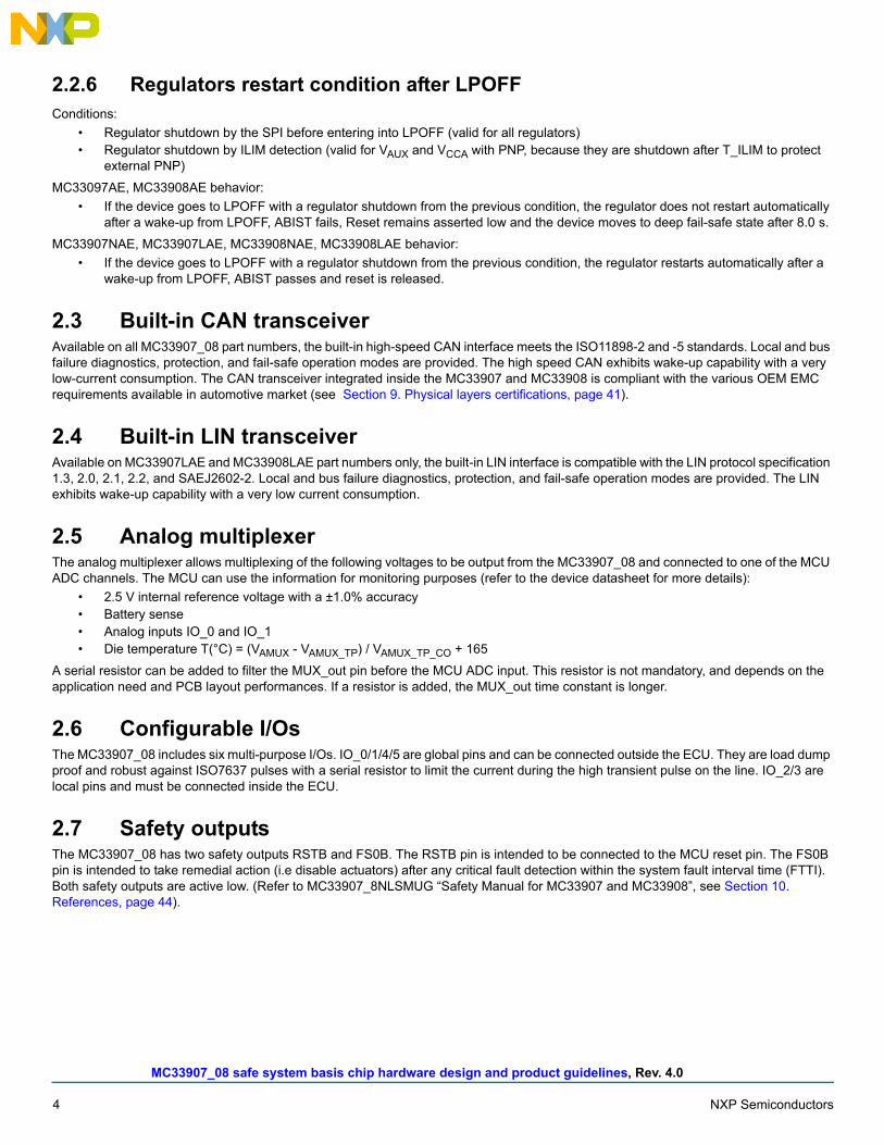
3 Application schematic
Figure 3. Application schematic
VSUP1
SW_PRE2
VPRE
SW_CORE
FB
_C
OR
E
VC
CA
_E
VC
CA
_B
VC
CA
VA
UX
_E
VA
UX
_B
VA
UX
CA
N-5
V
Vse
nse
CO
MP
_CO
RE
VSUP2
MO
SI
MIS
OS
CL
KN
CS
RX
DT
XD
CA
NH
CA
NL
VD
DIO
SE
LE
CT
MU
X_
OU
T
INT
B
RS
TB
FS
0B
DE
BU
G
IO_
0
IO_1
IO_
2
IO_3
IO_
4
IO_5
MC
3390
7_08
BOOT_PRE
GATE_LS
SW_PRE1
VC
OR
E_
SN
S
GN
D_C
OM
Vsu
p3
Vb
at
1 µ
H
4.7 µF
22 µF
5.1
k
1µF
22 µ
H
10 µF
10 µF
1µ
F
2.2
µH
100nF
R3
R4
C1
R1
R2
C2
4M
CU
SP
I
VD
DIO
MC
U R
ES
ET
MC
U C
AN
10 nF
5.1
K
1 nF
MC
U In
t.
To
Fai
l Saf
e ci
rcui
try
CAN BUS
120
4.7µF
RS
elec
t
SELECT
pin Con
figuration for V
CCA & VAU
X(R select con
nected
to GND)
Vcca
Vaux
Rselect (K
) Re
commen
ded Va
lue
3.3V
3.3V
< 7
5.1K
+
/-5%
5V
5V
10.8 <<13.2
12K
+/-
5%3.3V
5V
21.6 <<26.4
24K
+/-
5%5V
3.3V
45
.9<<56.1
51K
+/-
5%
Compo
nents s
electio
n for V
core voltage
(current ra
nge 10mA ‐> 800mA, DI/DT
= 2A/
µs)
Vcore vo
ltage
R3(+/‐1%
)R4
(+/‐1%
)R1
(+/‐5%
)C1
R2(+/‐5%
)C2
Cout
1.23V
4.32K
8
.06K
2
00
220
pF 39K
1nF
2*10
µF3.3V
24.9K
8
.06K
5
10
6
80pF
18K
150
pF 2*10
µF
MC
U in
puts
Vco
re V
olta
ge
1 nF
10 nF
4.7 µF
Vc
ca
(5V
or
3.3
V),
av
aila
ble
co
nfi
gu
rati
on
sW
hith
out E
xt. P
NP
: 10
0mA
cap
abili
ty +
/-1
% a
ccur
acy
for
5V
con
figu
ratio
n, +
/-1.
5% a
ccur
acy
for
3.3V
con
figu
ratio
n,
With
Ext
. PN
P :
< 2
00m
A +
/-2
% a
ccu
racy
With
Ext
. PN
P :
30
0mA
ca
pab
ility
+/-
3% a
ccur
acy
Va
ux
(5V
or
3.3
V)
30
0mA
cap
ab
ility
+/-
3% a
ccu
racy
MU
X_O
UT
(o
utp
ut
sele
cted
by
SP
I)V
sen
se o
rV
IO_
0 o
r V
IO_
1 o
r In
tern
al 2
.5V
re
fere
nce
vo
ltage
(2
.5V
+/-
1%
) o
rT
em
p
Con
nect
ed to
Vcc
a or
Vco
re(I
f co
nnec
ted
to V
core
, mus
t be
co
nnec
ted
clos
ed t
o co
utx
10µ
F x
2)
VD
DIO
or V
SU
P3
5.1
K
if co
nnec
ted
to V
DD
IO>
10K
if co
nnec
ted
to V
sup
3
5.1
K
4.7 µF
100nF
10 µF
10 µF
10 µF
100nF
2.2nF 8
PG
ND
PG
ND
PG
ND
PG
ND
PG
ND
GN
D
GN
D
GN
D
PG
ND
PG
ND
PG
ND
PG
ND
PG
ND
PG
ND
GN
D
GN
D
GN
D
GN
D
GN
DGN
D
GN
D
PG
ND
GN
D
GN
D
Gro
un
d C
on
nec
tio
ns
PG
ND
gro
und
pla
ne c
on
nec
ted
to D
GN
D p
inG
ND
gro
un
d p
lan
e c
onn
ect
ed
to A
GN
D a
nd G
ND
_CO
M p
ins
PG
ND
(D
GN
D)
and
GN
D (
AG
ND
& G
ND
_C
OM
) co
nne
cte
d to
geth
er
far
fro
m
PG
ND
gro
un
d p
lan
e.G
ND
10 nF
Vpr
e
DE
BU
G
mod
e
GN
D
GN
D
GN
DA
GN
D
DG
ND
ES
R c
ap.
<10
0m
ES
R c
ap.
<10
m
ES
R c
ap.
<10
m
ES
R c
ap.
<10
0m
ES
R c
ap.
<10
0m
Va
ux_
PN
P
Vcc
a_P
NP
11K
5.1
k
FC
CU
mon
itori
ngfr
om F
rees
cale
M
CU
Opt
iona
l
Opt
iona
l
Opt
iona
l
10 µF PG
ND
22 µF
EM
I su
p. C
apac
itor
mus
t be
con
nect
ed
clos
ed t
o lo
ad (
220
nF)
and
conn
ecte
d to
G
ND
EM
I su
p. C
apac
itor
mus
t be
con
nect
ed
clos
ed t
o lo
ad (
100
nF +
100
pF)
and
conn
ecte
d to
GN
D
100 nF GN
D
GN
D
1K
2.2nF 7.5 PG
ND
0R
Vb
at
Opt
iona
l
Rec
omm
ende
d co
nnec
tion
for
IOs
not
used
in th
e ap
plic
atio
n
Exa
mpl
e of
IO
conn
ectio
n an
d us
age
5.1
k
5.1
k
Cap
acito
r m
ust b
e cl
ose
to V
aux
pin
Cap
acito
r cl
osed
to
Vcc
a pi
n
Res
isto
r m
ust b
e cl
ose
to S
elec
t pi
n
Cap
acito
rs m
ust
be c
lose
to
Vpr
e pi
n
GN
D
GN
D
10K
22 pF
330
pF
GN
D
Key
on
BOOT_CORE
Snu
bber
val
ues
mus
t be
fin
e tu
ned
as
linke
d al
so t
o bo
ard
layo
ut p
erfo
rman
ce
Snu
bber
val
ues
mus
t be
fin
e tu
ned
as
linke
d al
so t
o bo
ard
layo
ut p
erfo
rman
ce

MC33907_08 safe system basis chip hardware design and product guidelines, Rev. 4.0
8 NXP Semiconductors
Optional configurations
4 Optional configurationsAccording to customer application needs, optional configurations for the MC33907_08 are described by the following sections.
4.1 Pre-regulator, buck or buck-boost configurationTwo topologies are available on the MC33907_08 for the VPRE pre-regulator. The MC33907_08 can be configured in buck only or buck-boost converter mode according to the GATE_LS pin connection. The detection is done automatically during the startup sequence, from power on reset or after each wake-up from LPOFF.
Figure 4. Buck-boost configuration
Figure 5. Buck configuration
In buck only configuration, the external low-side MOS and the diode are removed, and the Gate_LS pin must be connected to ground (PGND or GND).
SW
_PR
E2
VP
RE
GA
TE
_LS
SW
_PR
E1
22 H
100
nF2.2
nF
8.0
PGND
PGND
PGND
Optional
10 µ
F
10
µF
10 µ
F
PGND PGND PGND
ESR cap.<100 m
ESR cap.<10 m
10
µF
PGND
Snubber values must be fine tuned as linked also to board layout performance
BO
OT
_PR
E
SW
_PR
E2
VP
RE
GA
TE
_LS
SW
_PR
E1
22 H
22 µ
F
10 µ
F
100
nF
22 µ
F
2.2
nF
8.0
PGNDPGND PGND PGND
PGND PGND
ESR cap.
<100 m
ESR cap.
<10 m
Snubber values must be fine tuned as linked also to board layout performance
BO
OT
_P
RE
MC33907_08 safe system basis chip hardware design and product guidelines, Rev. 4.0
NXP Semiconductors 9
Optional configurations
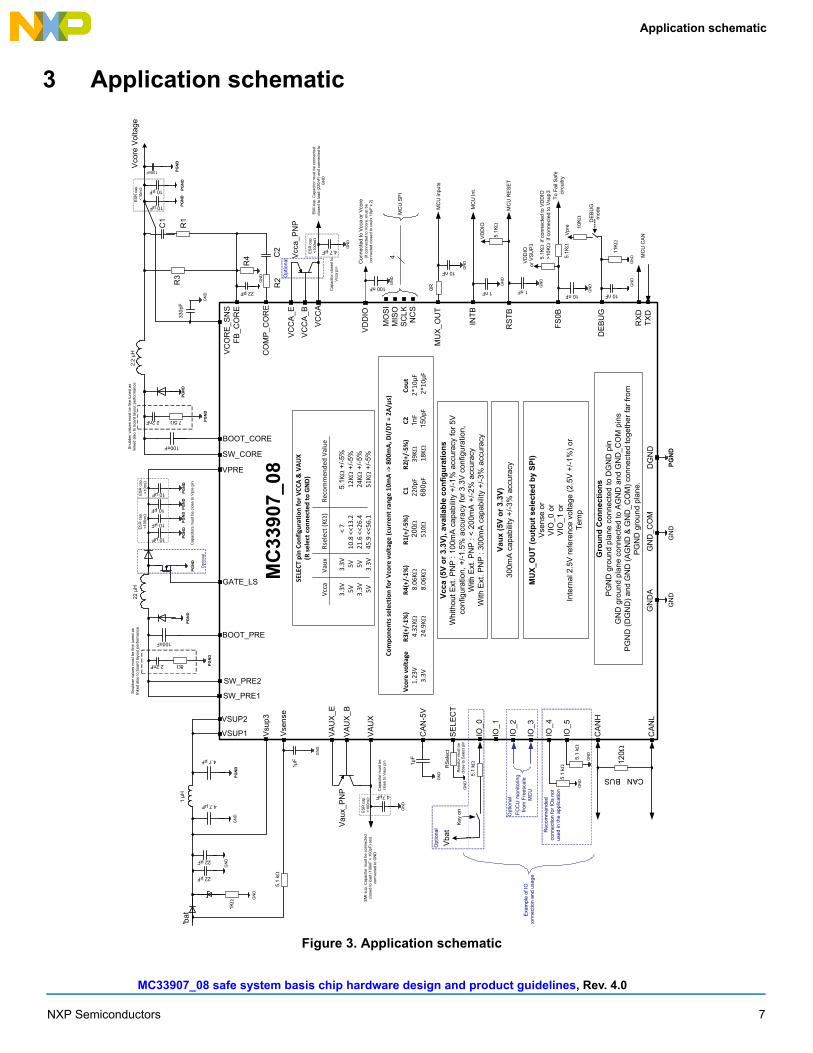
4.2 VCCA, current capabilityTo increase the current capability from 100 mA to 300 mA on the VCCA linear regulator, an external PNP transistor must be connected. Using an external PNP increases the current capability and reduces the accuracy from ±1.0% at 100 mA to ±3.0% at 300 mA.
Figure 6. VCCA current capability 300 mA, ±3.0% accuracy
Figure 7. VCCA current capability 100 mA, ±1.5% (3.3 V), ±1.0% (5.0 V)
When no external PNP is connected to VCCA, the VCCA_E pin must be connected to the VPRE pin.
4.3 VAUXDepending on application needs, the auxiliary regulator can be used. The following figures show the correct connections of VAUX in both cases. The external PNP is mandatory.
Figure 8. VAUX current capability 300 mA, 3.0% accuracy
VCCA_E
VCCA_B
VCCA
4.7μ
F
GND
ESR cap.<100 m�
VCCA_PNPOptional
EMI sup. Capacitor must be connected closed to load (220 nF) and connected to
GND
VCCA
4.7
µF
GND
ESR cap.
<100 m
VPRE
NC
VCCA_E
VCCA_B EMI sup. Capacitor must be connected closed to load (220 nF) and connected to
GND
VAUX_E
VAUX_B
VAUX
4.7
µF
GND
ESR cap.<100m
Vaux_PNP
EMI sup. Capacitor must be connected closed to load (220nF) and connected to
GND

MC33907_08 safe system basis chip hardware design and product guidelines, Rev. 4.0
10 NXP Semiconductors
Optional configurations
Figure 9. VAUX connections if not used
When VAUX is not used, the VAUX_E and SELECT pins must be connected to the VPRE pin.
4.4 IO_0 ignition connectionIn automotive applications, it is recommended to connect IO_0 to ignition to be able to recover from deep fail-safe state by a key OFF, Key ON action.
4.5 IO_1 FB_CORE monitoringWhen the application targets the ISO26262 ASIL D safety level, it is recommended to monitor the VCORE output voltage through IO_1. In this case, a second resistor bridge is needed, which is a duplication of the R3/R4 external resistor bridge used to create VCORE from FB_CORE. Available on MC33907NAE, MC33907LAE, MC33908NAE, and MC33908LAE part numbers only, refer to the MC33907_8NLSMUG safety manual for more information.
4.6 IO_2 and IO_3, FCCU monitoringIO_2 and IO_3 can be configured as safety inputs to allow monitoring of the NXP microcontroller FCCU output pins FCCU_E[0] and FCCU_E[1].
Figure 10. IO_2 and IO_3 configured as safety inputs
IO_2 should be connected to FCCU_EF[0] and IO_3 to FCCU_E[1]. A pull-up resistor must be connected to IO_3/FCCU_E[1] and a pull-down resistor to IO_2/FCCU_E[0]. Bi-stable protocol only from MCU is supported. (Refer to MC33907_8NLSMUG “Safety Manual for MC33907 and MC33908”, see Section 10. References, page 44). If not used, IO_2 and IO_3 can be left open or pulled down to GND.
VAUX_E
VAUX_B
VAUX
SELECTRSelect
VPRE
NC
NC
IO[2]
IO[3]
GND
Rpd2
Rpu3
VDDIO
FCCU_E[1]
FCCU_E[0]
Optional FCCU monitoringfrom Freescale MCU

MC33907_08 safe system basis chip hardware design and product guidelines, Rev. 4.0
NXP Semiconductors 11
MC33907_08 external components
5 MC33907_08 external componentsThis section is based on Figure 3, and details how to select the external components. It also proposes some references and tolerances needed to ensure optimal performance of the system. All the recommended components are based on NXP use case validations.
5.1 MC33907_08 power supplyPower to the MC33907_08 is provided by the VSUP1, VSUP2, and VSUP3 supply pins. An external reverse battery protection diode must be connected between the VBAT external battery input and the capacitor input filter.
A PI filter is implemented to avoid current switching noises coming from DC/DC converters to be propagated to VBAT and VSUP3 supplies. For that reason, VSUP3 must be connected before the PI filter to deliver a clean supply to the MC33907_08, de-correlated from the VSUP1 and VSUP2 dedicated to VPRE SMPS pre-regulator.
The total capacitor (CBAT1 + CBAT2) between the VBAT and VSUP pins must be greater than 44 µF, to limit the slew rate on VSUP pins in case of a high transient. The resistor connected to VSENSE is mandatory to limit the current at the pin, in case of a high transient (positive and negative).
If the application has to sustain ISO pulses on VBAT in LPOFF mode, the connection of a an external zener diode (DIP) and a serial resistor to the ground (RIP) is needed to discharge the CBAT capacitors.
If the application has to pass J2962 certification for the American automotive market, a ferrite bead (FB) on the VBAT line is recommended to pass the radiated emission test.
The MC33907_08 power connection is shown in Figure 11.
Figure 11. Power supply connection
The PI filter has a resonance frequency at with a filtering slope at -40 dB per decade.
The pre-regulator VPRE is the main contributor to the noise reported to VBAT. The resonance frequency of the PI filter must be f_res < VPRE switching frequency (f_res < FSWPRE < 440 kHz). All MC33907_08 validations and EMC certifications have been successfully passed with LPI = 1.0 H and CPI = 4.7 F, giving a resonance frequency f_res = 73 kHz. The resonance frequency of the PI filter can be adjusted at the application level to improve EMC performances.
VS
UP
1
VSENSE
VS
UP
2
VSUP3
Vbat
LPI
CP
I2
Cb
at1
Rsense
Cse
nse
CP
I1
PGNDGND GND
GND
MC33907_08
RP Diode
GND
Rip
Dip Cb
at2
FB
f_res1
2 LPI CPI-----------------------------------------=

MC33907_08 safe system basis chip hardware design and product guidelines, Rev. 4.0
12 NXP Semiconductors
MC33907_08 external components
5.2 MC33907_08 VPRE pre-regulatorThe pre-regulator VPRE delivers a 6.5 V typical output voltage.
• In buck only configuration, the Gate_LS pin must be tied to PGND or GND. • In buck-boost configuration, an external logic level MOSFET (N-type) must be connected to the Gate_LS pin and an additional
diode is needed, as shown in Figure 4.
The three capacitors in parallel (COUT_VPRE1, COUT_VPRE2, and COUT_VPRE3) can be replaced by two 22 F in parallel, or even one 47 F capacitor, but with always ESR < 100 m. The pre-regulator connections are shown in Figure 12.
Figure 12. VPRE connections
Table 1. Power supply component list
Component Value Reference/manufacturer proposal Ground connection
FB MPZ1608S101ATAH0/TDK
RP Diode
MBR5H100MFS/On Semiconductor (IF=5A, VR=100V)PMEG10030ELP/NXP (IF=3A, VR=100V)PMEG10020ELP/NXP (IF=2A, VR=100V)PMEG10010ELR/NXP (IF=1A, VR=100V)SBRS81100T3G/On Semiconductor (IF=2A, VR=100V)
Dip Zener 30 V BZX384C/NXP
Rip 1.0 k GND
Cbat1 22 µF GND
Cbat2 22 µF GND
CPI1 4.7 µF GCM32ER71H475K/Murata GND
LPI 1.0 µH B82472G6102M000/TDK-EPCOS
CPI2 4.7 µF GCM32ER71H475K/Murata PGND
Rsense 5.1 k
Csense 1.0 µF CGA5L3X7R1H105K/Murata GND
SW
_PR
E2
VP
RE
BO
OT
_PR
E
GA
TE
_LS
SW
_PR
E1
L_Vpre
Cbo
ot_
pre
Csn
ub_V
pre
Rsu
nb_V
pre
PGND
PGND
MC33907_08
PGND
Optional
D_V
pre
LS
_BB
D_BB
PGND PGND PGND
ESR cap.
<100 m ESR cap.<10 m
PGND
Cou
t_V
pre1
Cou
t_V
pre
2
Cou
t_V
pre
3
Co
ut_V
pre4

MC33907_08 safe system basis chip hardware design and product guidelines, Rev. 4.0
NXP Semiconductors 13
MC33907_08 external components
5.2.1 VPRE main characteristics• VSUPMAX = 40 V• VSUPMIN = 2.7 V• VPRE = 6.5 V• VPRE_MAXRATING = 8.0 V• IPREMAX = 2.0 A• IPREMIN = 0.3 A (in boost mode when VSUP < 4.0 V)• FSWPRE = 440 kHz
5.2.2 L_VPRE calculation• Inductor current ripple: IRIP = K x IPREMAX = 0.6 A with K = 0.3 (30% of IPRE)
• Buck configuration:
• Boost configuration:
• From calculation, L_VPRE = 20.6 H in buck mode and L_VPRE = 16.6 H in boost mode• From normalized value, recommended L_VPRE = 22 H
• The current discharge slope in the inductor is . With VPRE = 6.5 V and L_VPRE = 22 µH, ISLOPE = -300 mA/µs.
• VPRE is a current mode controlled SMPS with a -500 mA/µs internal slope compensation to avoid sub-harmonic oscillations when the duty cycle is >50%. A minimum L_VPRE must be chosen to maintain the current discharge slope in the inductor lower than the internal slope compensation.
5.2.3 L_VPRE selection• Must be shielded inductor• Inductor value: 22 H
Figure 13. Peak current in the inductor
LVpreVpre Vsupmax Vpre–
K Vsupmax Ipremax Fswpre-----------------------------------------------------------------------------------------=
LVpreVsupmin2 Vpre Vsupmin– K Vpre2 Ipremin Fswpre
-------------------------------------------------------------------------------------=
Vpre–LVpre-----------------
Boost mode Buck mode only

MC33907_08 safe system basis chip hardware design and product guidelines, Rev. 4.0
14 NXP Semiconductors
MC33907_08 external components
• Buck mode only: — rated current: IR > IPREMAX > 2.0 A— saturation current: ISAT > IR + (IRIP /2) > 2.3 A
• Buck/boost mode (80% efficiency considered in boost mode):— rated current: IR > ISUP > 2.7 A— saturation current: ISAT > ISUP + (IRIP /2) > 3.1 A
• Serial resistance: DCR < 100 m
5.2.4 D_VPRE selection:• Schottky diode is recommended
– lower forward voltage drop (VF) reduces power dissipation– lower parasitic capacitor improves EMC performance
• Reverse voltage: VR VSUPMAX 40 V• Average rectified forward current: IF > IPREMAX + (IRIP /2) > 2.3 A• Power dissipation: PD = VF x IF
5.2.5 LS_BB selection:• Must be logic level N-type MOSFET • Low RDS(on) reduces conduction losses• Drain source voltage: VDS > VPRE_MAXRATING + VF(D_BB) > ~9.0 V• Drain current: IDS > IPREMAX + (IRIP /2) > 2.3 A
• Gate source capacitance: . With IBOOST = 300 mA and TRISE = 30 ns, CGS = 1.5 nF
5.2.6 D_BB selection• Schottky diode is recommended
– lower forward voltage drop (VF) reduces power dissipation– lower parasitic capacitor improves EMC performance
• Reverse voltage: VR VPRE_MAXRATING 8.0 V• Average rectified forward current: IF > IPREMAX + (IRIP /2) > 2.3A• Power dissipation: PD = VF x IF
5.2.7 Output capacitors• 40 F ceramic capacitor(s) with low ESR << 100 m is recommended• The ESR of the output capacitor is one of the main contributor to the output voltage ripple. The ripple generated by the ESR is
proportional to its value (ESR * IRIP). A high ripple can disturb the regulation loop.• Low ESR capacitors reduces the ripple, avoid instability and lower EMI.
5.2.8 SnubberIn asynchronous SMPS, a freewheeling diode is used to discharge the inductor (during recirculation phase). When this diode is turned OFF (corresponding to when the MOS is turned ON), some oscillations happen due to the leakage inductance and output capacitance of the diode plus the PCB layout parasitics. A RC snubber in parallel to the diode dampens these oscillations and lower EMI (see the damping effect of a well designed snubber in Figure 14).
CgsIboost Trise
Vpre-----------------------------------------=
MC33907_08 safe system basis chip hardware design and product guidelines, Rev. 4.0
NXP Semiconductors 15
MC33907_08 external components
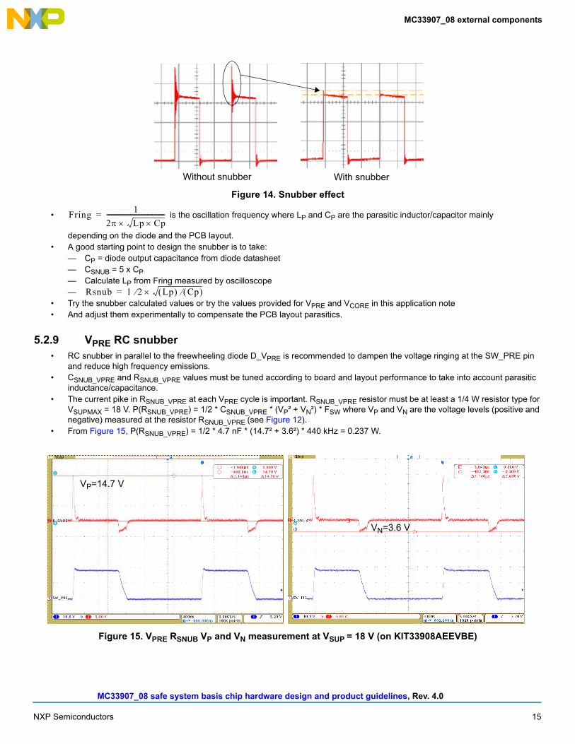
Figure 14. Snubber effect
• is the oscillation frequency where LP and CP are the parasitic inductor/capacitor mainly depending on the diode and the PCB layout.
• A good starting point to design the snubber is to take:— CP = diode output capacitance from diode datasheet— CSNUB = 5 x CP— Calculate LP from Fring measured by oscilloscope—
• Try the snubber calculated values or try the values provided for VPRE and VCORE in this application note• And adjust them experimentally to compensate the PCB layout parasitics.
5.2.9 VPRE RC snubber• RC snubber in parallel to the freewheeling diode D_VPRE is recommended to dampen the voltage ringing at the SW_PRE pin
and reduce high frequency emissions. • CSNUB_VPRE and RSNUB_VPRE values must be tuned according to board and layout performance to take into account parasitic
inductance/capacitance.• The current pike in RSNUB_VPRE at each VPRE cycle is important. RSNUB_VPRE resistor must be at least a 1/4 W resistor type for
VSUPMAX = 18 V. P(RSNUB_VPRE) = 1/2 * CSNUB_VPRE * (VP² + VN²) * FSW where VP and VN are the voltage levels (positive and negative) measured at the resistor RSNUB_VPRE (see Figure 12).
• From Figure 15, P(RSNUB_VPRE) = 1/2 * 4.7 nF * (14.7² + 3.6²) * 440 kHz = 0.237 W.
Figure 15. VPRE RSNUB VP and VN measurement at VSUP = 18 V (on KIT33908AEEVBE)
Without snubber With snubber
Fring1
2 Lp Cp-------------------------------------=
Rsnub 1 2 Lp Cp =
VP=14.7 V
VN=3.6 V

MC33907_08 safe system basis chip hardware design and product guidelines, Rev. 4.0
16 NXP Semiconductors
MC33907_08 external components
5.2.10 Continuous mode• VPRE must work in continuous mode (current in the inductor always > 0) for a good stability and good EMC performances• VPRE is in continuous when IPRE > 180 mA (for a 22 H inductor)• IPRE = ICCA + IAUX + ICAN + (ICORE * VCORE / VPRE / VCORE_EFF) where VCORE_EFF is VCORE efficiency (~85% at 3.3 V and ~70%
at 1.2 V)
5.2.11 VSUP slow ramp upThe VPRE pre-regulator is connected to VSUP. Very slow VSUP ramp up could influence the start-up of the pre-regulator in buck mode only. During the start-up phase in buck mode only, VPRE follows VSUP when VSUP_UV_5 < VSUP < 6.5 V.
When VPRE > VPRE_UV, all the regulators start (VCORE, VCCA, VAUX, and CAN_5V) and sink current from VSUP, creating a voltage drop thru the reverse battery diode and the input filter.
VPRE may decrease below VPRE_UV, depending on application components and layout, and may take more than 8.0 s to recover, sending the device into deep fail-safe due to reset stuck during the > 8.0 s recovery.
In case the application must start with a very slow VSUP ramp up down to 0.5 V/min, it is recommended to implement the boost mode of the pre-regulator VPRE. In this case, VPRE starts in boost mode when VSUP > VSUP_UV_5 and gives more room to VPRE_UV when the regulators starts.
5.2.12 Component list proposal
Table 2. VPRE supply component list
Component Value Reference/manufacturer proposal Ground connection
CSNUB_VPRE 2.2 nF
RSNUB_VPRE 8.0 PGND
CBOOT_PRE 100 nF
D_VPRE
- MBRS340T3/ON Semiconductor (IF = 3.0 A, VR = 40 V)- SS24T3G/On Semiconductor (IF = 2.0 A, VR = 40 V)- PMEG4030EP/NXP (IF = 3.0 A, VR = 40 V)- PMEG4020EP/NXP (IF = 2.0 A, VR = 40 V)
PGND
L_VPRE 22 H- B82479G1223M/TDK-EPCOS (IR = 3.1 A, ISAT = 6.0 A)- B82464G4223M/TDK-EPCOS (IR = 2.25 A, ISAT = 2.5 A)- MSS1278-223MLB/COILCRAFT (IR = 4.0 A, ISAT = 6.0 A)
(1)
LS_BB- BUK9832-55A/NXP- BUK9M26-60E/NXP
PGND
D_BB
- MBRS340T3/ON Semiconductor (IF = 3.0 A, VR = 40 V)- SS24T3G/On Semiconductor (IF = 2.0 A, VR = 40 V)- PMEG4030EP/NXP (IF = 3.0 A, VR = 40 V)- PMEG4020EP/NXP (IF = 2.0 A, VR = 40 V)
COUT_VPRE1 10 FCeramic capacitor ESR<100 mCGA6M3X7R1C106K/TDK
PGND
COUT_VPRE2 10 FCeramic capacitor ESR<100 mCGA6M3X7R1C106K/TDK
PGND
COUT_VPRE3 10 FCeramic capacitor ESR < 100 mCGA6M3X7R1C106K/TDK
PGND
COUT_VPRE4 10 FCeramic capacitor ESR < 10 mCGA6M3X7R1C106K/TDK
PGND
Notes: 1. In buck mode only configuration

MC33907_08 safe system basis chip hardware design and product guidelines, Rev. 4.0
NXP Semiconductors 17
MC33907_08 external components
5.3 MC33907_08 VCORE supply regulatorThe core supply regulator is configurable from 1.2 V to 3.3 V range and adjustable around these voltages with an external resistor bridge (R3 and R4). An external compensation network made of R1, C1, R2, and C2 is connected between VCORE_SNS, FB_CORE, and COMP_CORE to ensure a good stability of the closed loop. The core supply connections are shown in Figure 16.
Figure 16. VCORE connections
5.3.1 VCORE main characteristics• VPREMAX = 7.0 V• VPRE_MAXRATING = 8.0 V• VCOREMAX = 3.3 V• ICOREMAX = 1.5 A for MC33908, ICOREMAX = 0.8 A for MC33907• FSWCORE = 2.4 MHz
5.3.2 L_VCORE calculation• Inductor current ripple: IRIP = K x ICOREMAX = 0.45 A with K = 0.3 (30% of ICORE)
• Buck configuration:
• From calculation, for VCORE = 3.3 V/1.5 A, L_VCORE = 1.62 H• From normalized value, recommended L_VCORE = 2.2 H
5.3.3 L_VCORE selection• Must be shielded inductor• Inductor value: 2.2 H• Rated current: IR > ICOREMAX > 1.5 A• Saturation current: ISAT > IR + (IRIP /2) > 1.73 A• Serial resistance: DCR < 50 m
SW
_CO
RE
FB_CORE
COMP_CORE
BO
OT_C
OR
E
VCORE_SNS
L_VCORE
Cbo
ot_C
ore
R3
R4
C1
R1
R2 C2
Cou
t1_V
core
EM
IC
out_
Vco
re
PGND
PGND
PGND PGND
PGND
GND
ESR cap.<100 m�
D_V
core
Csn
ub_V
core
Cou
t2_V
core
Rsn
ub_V
core
GND
GND
EM
IV
core
_sns
EM
IFB
_cor
e
VCORE Voltage
LVcoreVcore Vpremax Vcore–
K Vpremax Icoremax Fswcore-----------------------------------------------------------------------------------------------=

MC33907_08 safe system basis chip hardware design and product guidelines, Rev. 4.0
18 NXP Semiconductors
MC33907_08 external components
5.3.4 D_VCORE selection• Schottky diode is recommended
– lower forward voltage drop (VF) reduces power dissipation– lower parasitic capacitor improves EMC performance
• Reverse voltage: VR VPRE_MAXRATING 8.0 V• Average rectified forward current: IF > ICOREMAX + (IRIP /2) > 1.73 A• Power dissipation: PD = VF x IF
5.3.5 Output capacitors• 20 F ceramic capacitor(s) with low ESR << 100 m is recommended for the MC33907.• 40 F ceramic capacitor(s) with low ESR << 100 m is recommended for the MC33908.• The ESR of the output capacitor is one of the main contributor to the output voltage ripple. The ripple generated by the ESR is
proportional to its value (ESR * IRIP). A high ripple can disturb the regulation loop.• Low ESR capacitors reduces the ripple, avoid instability and lower EMI.
5.3.6 VCORE RC snubber• An RC snubber in parallel to the freewheeling diode D_VCORE is recommended to dampen the voltage ringing at SW_CORE pin
and reduce high frequency emissions.• CSNUB_VCORE and RSNUB_VCORE values must be tuned according to board and layout performance to take parasitic
inductance/capacitance into account. • The current pike in RSNUB_VCORE at each VCORE cycle is important. The RSNUB_VCORE resistor type must be at least 1/4 W.
P(RSNUB_VCORE) = 1/2 * CSNUB_VCORE * (VP² + VN²) * FSW where VP and VN are the voltage levels (positive and negative) measured at the resistor RSNUB_VCORE (see Figure 16).
Figure 17. VCORE RSNUB VP and VN measurement (on KIT33908AEEVBE)
• From Figure 17, P(RSNUB_VPRE) = 1/2 * 4.7 nF * (5.4² + 3.12²) * 2.4 MHz = 0.219 W.
5.3.7 Continuous mode• VCORE must work in continuous mode (current in the inductor always > 0) for a good stability and good EMC performances• For VCORE = 3.3 V configuration, VCORE is in continuous when ICORE > 160 mA (for a 2.2 H inductor)• For VCORE = 1.2 V configuration, VCORE is in continuous when ICORE > 120 mA (for a 2.2 H inductor)
VP=5.4 V
VN=-3.12 V

MC33907_08 safe system basis chip hardware design and product guidelines, Rev. 4.0
NXP Semiconductors 19
MC33907_08 external components
5.3.8 Compensation networkVCORE is a voltage mode buck converter with two poles and needs a compensation network which creates a large phase boost. Such amplifier circuit is called “type 3 amplifier compensation”. It gives a very good transient response to the circuit.
The compensation network connection is shown Figure 18 and the “AN4661: Designing the VCORE compensation network” covers this subject in detail. In addition, a simulation tool is available to optimize IC performance for specific use cases.
The compensation network R1, C1, R2, and C2 is external to be flexible. It can be tuned to attach the MC33907_8 to a different MCU. Only C3, which is a very small capacitor value, is internal. A simulation tool, based on Matlab model, can be provided on demand to support optimized compensation network design.
Component values for VCORE 3.3 V and 1.2 V configurations are provided in the datasheet and in the Figure 3 application schematic.
Figure 18. VCORE compensation network
5.3.9 Component list proposal
Table 3. VCORE supply component list
Component Value Reference/manufacturer proposal Ground connection
CBOOT_CORE 100 nF
CSNUB_VCORE 2.2 nF
RSNUB_VCORE 7.5 PGND
D_VCORE
- SS22T3G/ON Semiconductor (IF = 2.0 A, VR = 20 V)- PMEG3020EH/NXP (IF = 2.0 A, VR = 30 V)- PMEG3020EP/NXP (IF = 2.0 A, VR = 30 V)- PMEG3020ER/NXP (IF = 2.0 A, VR = 30 V)
PGND
L_VCORE 2.2 H B82472G6222M000/TDK-EPCOS
R3 4.32 k±1%Configuration for VCORE = 1.23 V
R4 8.06 k±1% GND
R1 200 ±5%
Current up to 800 mAC1 220 pF ±10%
R2 39K ±5%
C2 1.0 nF ±10%
R3 24.9 k±1%Configuration for VCORE = 3.3 V
R4 8.06 k±1% GND
R4
R3
R1 R2
VCORE_SNS
VREF
COMP_CORE
C1
C3
C2
FB
_CO
RE
GND
MC33907_08 safe system basis chip hardware design and product guidelines, Rev. 4.0
20 NXP Semiconductors
MC33907_08 external components
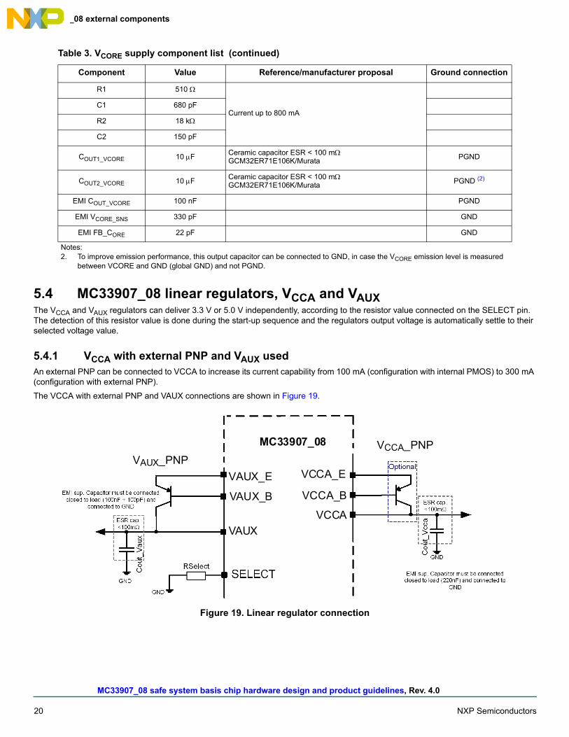
5.4 MC33907_08 linear regulators, VCCA and VAUXThe VCCA and VAUX regulators can deliver 3.3 V or 5.0 V independently, according to the resistor value connected on the SELECT pin. The detection of this resistor value is done during the start-up sequence and the regulators output voltage is automatically settle to their selected voltage value.
5.4.1 VCCA with external PNP and VAUX usedAn external PNP can be connected to VCCA to increase its current capability from 100 mA (configuration with internal PMOS) to 300 mA (configuration with external PNP).
The VCCA with external PNP and VAUX connections are shown in Figure 19.
Figure 19. Linear regulator connection
R1 510
Current up to 800 mAC1 680 pF
R2 18 k
C2 150 pF
COUT1_VCORE 10 FCeramic capacitor ESR < 100 mGCM32ER71E106K/Murata
PGND
COUT2_VCORE 10 FCeramic capacitor ESR < 100 mGCM32ER71E106K/Murata
PGND (2)
EMI COUT_VCORE 100 nF PGND
EMI VCORE_SNS 330 pF GND
EMI FB_CORE 22 pF GND
Notes: 2. To improve emission performance, this output capacitor can be connected to GND, in case the VCORE emission level is measured
between VCORE and GND (global GND) and not PGND.
Table 3. VCORE supply component list (continued)
Component Value Reference/manufacturer proposal Ground connection
MC33907_08
VAUX_B
VAUX
VCCA_E
VCCA_B
VCCA
VAUX_EVAUX_PNP
VCCA_PNP

MC33907_08 safe system basis chip hardware design and product guidelines, Rev. 4.0
NXP Semiconductors 21
MC33907_08 external components
5.4.2 PNP selection• VCCA PNP
– Collector-Emitter voltage: VCE VPRE_MAXRATING 8.0 V– Collector-Baser voltage: VCB VPRE_MAXRATING 8.0 V– Collector current: IC ICCA_LIM 675 mA– Current gain: 150 < HFE < 450– Power dissipation: Pd = (VPRE - VCCA) * ICCA = 1.0 W for VCCA = 3.3 V/300 mA
• VAUX PNP– Collector-Emitter voltage: VCE VSUPMAX 40 V– Collector-Baser voltage: VCB VSUPMAX 40 V– Collector current: IC IAUX_LIM 700 mA– Current gain: 100< HFE < 450– Power dissipation: PD = (VPRE - VAUX) * IAUX = 1.0 W for VAUX = 3.3 V/300 mA
5.4.3 Reduce Vaux_PNP power dissipationWhen VAUX is used at 3.3 V and high current, the power dissipation in the external PNP can be reduced by adding a resistance in serial with the PNP collector, as shown in Figure 20. RAUX reduces the drop in VAUX_PNP and its power dissipation.
Figure 20. Reduce VAUX_PNP power dissipation
VAUX_PNP voltage drop must be > 1.5 V so RAUX voltage drop must be less than VPRE - VAUX - 1.5 V < 1.7 V. RAUX must be < 4.0 .
RAUX value depends on IAUX and PDIS_RAUX to be balanced with PDIS_VAUX_PNP.
• Without RAUX: — PDIS_VAUX_PNP = (VPRE - VAUX) x IAUX = (6.5 V - 3.3 V) x 0.4 A = 1.3 W
• With RAUX = 3.0 : — PDIS_MAx = (VPRE - VAUX - (RAUX x IAUX)) x IAUX = (6.5 V - 3.3 V - (3 x 0.4)) x 0.4 A = 0.8 W— PDIS_RAUX = RAUX x IAUX
2 = 0.5 W
5.4.4 VAUX supplying a sensorWhen VAUX is used to supply a sensor outside the ECU, this regulator can be shorted to GND or shorted to battery at start-up, in case of a sensor failure. During the start-up phase of the MC33907_08, a VAUX_UV or VAUX_OV is detected during the ABIST verification and the device does not release its RSTB pin, preventing the MCU to start and diagnose the failure. Moreover, if the failure is permanent, the MC33907_08 moves to deep fail safe state after 8 s and shuts down all the regulators, awaiting for IO_0 transition to recover.
To avoid this behavior, a switch controlled by the MCU can be inserted between VAUX regulator and the Sensor input supply. This switch isolates VAUX from the Sensor, allowing the MC33907_08 to pass the ABIST verification and release its RSTB pin even in the case of Sensor failure during the start up phase. The MCU starts and then closes the switch M1 before starting the application.
VAUX_E
VAUX_B
VAUX
4.7
µF
GND
ESR cap.<100 m
VAUX_PNP
RAUX

MC33907_08 safe system basis chip hardware design and product guidelines, Rev. 4.0
22 NXP Semiconductors
MC33907_08 external components
Figure 21 illustrates a generic switch connection to isolate VAUX from the sensor input supply. Additional application specific components may be required. M1 can be replaced by a low VCEsat PNP transistor when MCU GPIO drives 3.3 V.
Figure 21. VAUX sensor supply with switch isolation
5.4.5 Component list proposal
Table 4. Linear Regulator Component List
Component Value Reference/manufacturer proposal Ground connection
VAUX_PNP
- NJT4030P/ON Semiconductor- PBSS5350Z/NXP- PHPT60603PY/NXP
COUT _VAUX 4.7 F ±10%Ceramic capacitor ESR < 100 mGCM31CR71C475KA37 / Murata
GND
D1 BZX84-C10/NXP
M1- PMOS: PMV250EPEA/NXP- PNP: PBSS5260QA/NXP
Q1 PBRN113ZT/NXP GND
VCCA_PNP
- NJT4030P/ON Semiconductor- PBSS5350Z/NXP- PHPT60603PY/NXP
COUT_VCCA 4.7 F ±10%Ceramic capacitor ESR < 100 mGCM31CR71C475KA37 / Murata
GND
Component Value VAUX/VCCA voltage configuration
RSELECT 5.1 k±5.0% VCCA = 3.3 V, VAUX = 3.3 V GND
RSELECT 12 k±5.0% VCCA = 5.0 V, VAUX = 5.0 V GND
RSELECT 24 k±5.0% VCCA = 3.3 V, VAUX = 5.0 V GND
RSELECT 51 k±5.0% VCCA = 5 V, VAUX = 3.3 V GND
RSELECT Open VCCA = 3.3 V, VAUX = 3.3 V
VAUX_E
VAUX_B
VAUX
4.7
µF
GND
Vaux_PNPSensor
MC33907_08
MCU
100k
10k
GPIO
M1
Q1
Vdd
GND
1µF
GNDD
1

MC33907_08 safe system basis chip hardware design and product guidelines, Rev. 4.0
NXP Semiconductors 23
MC33907_08 external components
5.4.6 VCCA without external PNP and VAUX not usedIf VAUX is not used in the application, the VAUX_E and RSELECT pins must be connected to the VPRE pin. The VAUX_B and VAUX pins can be left open. If VCCA is used without the external PNP, the VCCA_E pin must be connected to the VPRE pin. VCCA_B pin can be left open. The VCCA without an external PNP and VAUX unused connections are shown in Figure 22.
Figure 22. VAUX not used and VCCA w/o PNP
5.5 CAN_5VCAN_5V is a regulator dedicated to the internal physical layer. An external capacitor is needed for filtering purposes, as shown in Figure 23
Figure 23. CAN_5V connection
Table 5. RSelect component list
Component Value VCCA voltage configuration Ground connection
RSELECT 5.1 k±1.0% VCCA = 3.3 V GND
RSELECT 12.1 k±1.0% VCCA = 5.0 V GND
RSELECT 24.9 k±1.0% VCCA = 5.0 V GND
RSELECT 51.1 k±1.0% VCCA = 5.0 V GND
RSELECT Open VCCA = 3.3 V
VAUX_E
VAUX_B
VAUX
SELECTRSelect
NC
NC
VCCA
4.7µ
F
GND
ESR cap.<100m
VPRE
NC
VCCA_E
VCCA_B EMI sup. Capacitor must be connected closed to load (220nF) and connected to
GND
CAN_5V
Co
ut_C
AN
_5V
GND

MC33907_08 safe system basis chip hardware design and product guidelines, Rev. 4.0
24 NXP Semiconductors
MC33907_08 external components
5.6 Reset and fail-safe output, RSTB and FS0BThe RESET pin must be connected to the MCU reset pin. The MC33907_08 asserts RSTB low if a fault is reported. Refer to the datasheet for more information.
The FS0B pin is a safety output pin. In case of a major fault in the system, the MC33907_08 asserts FS0B low, disconnecting the critical functions in the application. FS0B is a global pin and can be connected outside the ECU. FS0B is load dump proof and robust against ISO7637 pulses with a serial resistor to limit the current during the high transient pulse on the line. RSTB and FS0B connections are shown in Figure 24.
Figure 24. Reset and fail-safe output connections
If FS0B is not used in the application, it is recommended to pull down this pin to GND with an external 10 K resistor, to avoid unexpected FS0B failure detection during ABIST or when an application is running.
In LPOFF mode, RSTB and FS0B are asserted low. If the FS0B pull-up is connected to VSUP3, expect some current through the pull-up resistor (VSUP3 / PU_FS0B) in addition to the MC33907_8 LPOFF current (32 A). This can be avoided by connecting the FS0B pull-up to VDDIO which is OFF in LPOFF mode.
Table 6. CAN_5V component list
Component Value Reference/manufacturer proposal Ground connection
COUT_VCAN 1.0 F CGA4J2X7R1C105K / TDK GND
Table 7. Reset and fail-safe output component list
Component Value Ground connection
COUT_RSTB 1.0 nF GND
PU_RSTB 5.1 k
COUT_FS0B 10 nF GND
RFS0B 5.1 k
PU_FS0B (if connected to VDDIO) 5.1 k
PU_FS0B (if connected to VSUP3) 10 k
RSTB
FS0B
VDDIO
MCU RESET
Co
ut_
FS
0b
R_FS0b
Cou
t_R
stb
To Fail Safe circuitry
VDDIO or Vsup3
Pu_
FS
0b
Pu
_Rst
b
GND
GND
EM
I_C
out_
FS
0b
GND
MC33907_08

MC33907_08 safe system basis chip hardware design and product guidelines, Rev. 4.0
NXP Semiconductors 25
MC33907_08 external components
5.7 MC33907_08 debug pinThe connections shown in Figure 25 can be used to enter into debug mode on the MC33907_08. Debug mode allows the user to debug software with the MCU. The deep fail-safe (regulator OFF, RSTB, and FS0B asserted low) and the WD timeout are disabled (fail-safe state machine). The CAN and the LIN are in normal mode by default (main state machine).
Figure 25. Debug mode entry connection
The Debug mode pin is scanned by the main and the fail-safe state machines at each power on reset. In the application, the main state machine is always powered by the battery while the fail-safe state machine is OFF in LPOFF mode. If the debug mode entry is done after release from LPOFF, only the fail-safe state machine is in debug mode with deep fail-safe and WD timeout disabled, not the main state machine. The CAN and LIN mode have to be configured to normal mode by the SPI.
Table 8. Debug mode component list
Component Value Ground connection
DBG_COUT 10 nF GND
DBG_RPD 11 k GND
DBG_RPU 10 k

MC33907_08 safe system basis chip hardware design and product guidelines, Rev. 4.0
26 NXP Semiconductors
MC33907_08 external components
5.8 MC33907_08 fail-safe start-up sequenceAfter a POR or a wake-up from LPOFF, the fail-safe state machine must be configured during the INIT_FS phase. Figure 26 illustrates the initialization process.
Figure 26. Fail-safe state machine initialization
1. Configure all the INIT_FS registers in regards to safety behavior expected on RSTB and FS0B at application level. Do not forget to disable IO_23_FS monitoring in INIT_FSSM2 register when IO_23 pins are not connected to FCCU pins of the MC, otherwise a reset generates when INIT_FS is closed by the first WD refresh.The INIT_FS phase is time limited to 256 ms maximum.
2. Refer to datasheet chapter 6.5.2.1 (see Section 10. References, page 44) for the watchdog answer calculation method. The first LFSR after POR or wake-up from LPOFF is always 0xB2. Consequently, the first seven good WD refresh required to close the INIT_FS phase and clear the reset error counter pin are: 0xD04D, 0xD19B, 0xD137, 0xD16E, 0xD1DC, 0xD1B9, and 0xD072. These WD_Answer SPI words are for reference and debug only. They must not be hard coded. The calculation method described in the datasheet must be followed to achieve the watchdog safety diagnostic coverage.
3. Refer to datasheet chapter 6.5.6 (see Section 10. References, page 44) for the FS_OUT register calculation based on WD_LFSR value to release the FS0B pin. Following the 7 WD refresh from step 2 (above), the FS_OUT register value to release FS0B pin is: 0xD327. This FS_OUT SPI word is for reference and debug only. It must not be hard coded. The calculation method described in the datasheet must be followed.
After step 2 (above), the watchdog must be periodically refreshed within the open window. Otherwise, a reset generates when the watchdog error counter reaches its final value (after 3 WD errors in default configuration, WD_ERR_CNT = 6).
The INIT phase of the main state machine is not time limited and can be handled when it is appropriate from an application standpoint. However, the INIT phase of the main state machine must be closed to allow CAN and LIN communications, MUX_OUT output selection, and transition to LPOFF by SPI command from the MCU.
Write all INIT_FS registers
Release FS0B pins
Send 7x good WD refresh 1st WD close INIT_FS
7th WD clear the RST_ERR_CNT)
Reset release from POROr Wake up from LPOFF
1
2
3

MC33907_08 safe system basis chip hardware design and product guidelines, Rev. 4.0
NXP Semiconductors 27
MC33907_08 extended use cases
6 MC33907_08 extended use cases
6.1 VSENSE accuracyVSENSE voltage, image of the battery voltage, can be monitored through the MUX_OUT pin with 5% accuracy out of the NXP production line (as specified in the datasheet). As described in Figure 27, this accuracy depends on the VSENSE resistor bridge and MUX_OUT amplifier offset, both varying with temperature, voltage, and process.
Figure 27. Simplified VSENSE to MUX_OUT block diagram
Statistical analysis shows the main contributor to the accuracy is the process variation which can be removed with a part to part calibration at customer production line test. The calibration can be done at room temperature, and static VSENSE between 9.0 V and 19 V (ideally 12 V or 14 V).
After calibration, the VSENSE monitoring accuracy can achieve 1%, for both VDDIO = 3.3 V and 5.0 V, in wide range resistor bridge configuration (without taking into account the VSENSE supply accuracy used for the calibration).
6.2 Wake-up by IOThe wake-up by IO is detected when a rising or a falling edge event happens at the IO pin and the device is in LPOFF mode. It means a transition from low to high or high to low must happen when the device is in LPOFF mode to validate the wake-up event.
If the IO wake-up event (rising or falling edge) arrives after the SPI LPOFF command and before the device entry to LPOFF, the wake-up event is not detected and the device does not wake-up. The device waits for the next IO transition to wake-up. See Figure 28 illustrating the IO_0 wake-up edge detection scenario.
Figure 28. Wake-up by the IO_0 edge
MUX_OUT
VSENSEExt. 5.1K
Perfectamplifier x1
Amplifier offset
Resistorbridge
Normal mode LPOFF mode
SPI CSB
SBC Sate Machine
IO_0
Wake up detected
Wake up not detected
Go to LPOFF SPI command

MC33907_08 safe system basis chip hardware design and product guidelines, Rev. 4.0
28 NXP Semiconductors
MC33907_08 extended use cases
At a 2.0 MHz SPI clock, the window where this could happen is less than 10 s. A work around is proposed in Figure 29 to avoid missing an IO wake-up event, as previously described.
Figure 29. Work around to wake-up by a IO_0 level
When IO_0 goes low, the MCU is informed through the IO_0 bit from IO_Input register. Before sending the LPOFF SPI command, the MCU activates the Q1 transistor to maintain IO_0 low during the SPI transmission and the device entry to the LPOFF process. When the MC33907_08 goes to LPOFF, all the regulators are shutdown. Q1 is released when the MCU is unpowered. If IO_0 moves to high during this short period, it is released and the IO_0 transition from low to high wakes up the device. This work around is applicable for all IOs.
6.3 MC33907 attach to Infineon Aurix MCUMC33907 can be attach to the Aurix MCU from Infineon. It has been validated with TC275 and TC277 versions and it is running in production. Figure 30 is a power tree proposal to show a possible connection between these two devices. This is not the only power tree possible, and can be adjusted depending on application need.
Figure 30. Power tree proposal
6.4 MC34FS6407_08 derivatives from MC33907_08Industrial MC34FS6407NAE and MC34FS6408NAE devices are derivatives from automotive MC33907NAE and MC33908NAE devices, qualified for 24 V DC input voltage up to a 36 V maximum operating voltage. All the hardware designs and product guidelines in this application note also apply to these industrial devices.The max. rating voltage is 40 V and an additional input protection is required to sustain a 60 V load dump in 24 V transportation applications.
Figure 31 is a companionship proposal for the MC34FS6407_08 to sustain this load dump requirement. The MAX6495 limits the input voltage at VOV (set here at 37.7 V) in order to not exceed the max. rating of the MC34FS6507_08 and keep the application running during the load dump condition.
SBCMC33907/8
MCUIO_0
GPIO
SPI
Q1
5.1K
VPREVSUP VCORE
1.25V – 0.8A
VAUX5V – 0.3A
VCCA3.3V – 0.1A
MC33907 TC2xxx
VDDVDD_OSCVDDSB
VAREF1,2VDD_MVERSBVEXT
VDD_OSC3VDDPVDDFLVFLEXAGBT_VDDFSB

MC33907_08 safe system basis chip hardware design and product guidelines, Rev. 4.0
NXP Semiconductors 29
MC33907_08 extended use cases
Figure 31. Battery connection proposal to sustain 60 V load dump
Table 9. MAX6495 external component list
Component Value Reference/manufacturer proposal Ground connection
ZD1- SMBJ54A/Fairchild- PTVS54VP1UP/NXP
GND
M1- BUK7275-100A/NXP- BUK7Y65-100E/NXP
VOV = 1.24 x (R1 / R2 + 1)
VS
UP
1
VSENSEV
SU
P2
VSUP3
VBAT1 µH
4.7
µF
5.1 k
1µF
4.7
µF
PGND
GND
GND
GND
47
µF
47 µ
F
GND
R2=24.9k
R1=732k
ZD
1
M1
100
nF
OUTFB
GND
GATE
IN
OVSET
SHDNb
MC34FS6407_08

MC33907_08 safe system basis chip hardware design and product guidelines, Rev. 4.0
30 NXP Semiconductors
PCB layout recommendations
7 PCB layout recommendationsTo minimize the effects of switching noise on the embedded DC/DC converters, special attention must be paid to the layout of the power components when designing a printed circuit board (PCB) using the MC33907_08.
Component locations and ground connections on the PCB are important to consider when successfully optimizing overall performance with regards to high transient current loops, as shown in Figure 32.
Figure 32. Current loops
7.1 Ground connectionsThree grounds are available on the MC33907_08:
• AGND (analog ground), • GND_COM (physical layer ground), and • DGND (logic ground).
On the PCB, two grounds must be clearly separated:
• Local PGND for power components involved in the high transient current loops • GND for other components connected to ground.
The star connection between PGND and GND must be done as far as possible from the local PGND ground on the PCB. The exposed pad is not electrically connected to ground, but this connection to the ground plane serves the power dissipation. The MCU digital ground should be connected to PGND to avoid any perturbation to GND. Each of the MC33907_08’s external component connections to adequate ground are listed in MC33907_08 external components. Connections from MC33907_08 grounds and PCB grounds are shown in Figure 33.
DUT PGND
PGND
GND
PGNDGND
Battery VSUP VSW_CORE
AGND
G_LSVSWR
C S
nubb
er

MC33907_08 safe system basis chip hardware design and product guidelines, Rev. 4.0
NXP Semiconductors 31
PCB layout recommendations
Figure 33. Ground connections between MC33907_08 and PCB ground
7.2 Routing external componentsIt is important to minimize the current loop on the PCB as much as possible. One way to do this is to place the power stage components involved in the high transient current loop as close as possible to the device. Avoid placing any power stage components close to other components which need to drive low current levels. Such components could easily be perturbed by switching noise.
7.2.1 The VPRE Pre-regulatorBased on Figure 12, the PGND line of D_VPRE is connected close to the PGND line near the COUT_VPRE(n) capacitors. COUT_VPRE(n) is kept close to the VPRE pin. The snubber (CSNUB_VPRE, RSNUB_VPRE) is kept close to D_VPRE.
7.2.2 The VCORE supply regulatorBased on Figure 16, the PGND line of D_VCORE is connected close to the PGND line of the COUT_VCORE(n) capacitors. The snubber (CSNUB_VCORE, RSNUB_VCORE) is kept close to D_VCORE. MC33907_08 VCORE output must be connected close to the MCU core supply input to avoid DC voltage drop in the PCB track.
7.2.3 VAUX, VCCA linear regulatorsBased on Figure 19, Cout _Vaux is kept close to the VAUX pin. COUT_VCCA is kept close to the VCCA pin.
7.2.4 VCANBased on Figure 23, keep COUT_CAN_5V close to the CAN_5V pin.
7.2.5 RSELECTBased on Figure 19, RSELECT must be placed close to the SELECT pin. Avoid power stage components close to the RSELECT pin so as not disturb the current in the resistor during startup. (This is the resistor used for VCCA and VAUX voltage configuration).
MC33907_08
AGNDGND_COM
DGND
PGND
6
45
PCB
VBAT+
VBAT-MCU
DNGD
GND
16
GND

MC33907_08 safe system basis chip hardware design and product guidelines, Rev. 4.0
32 NXP Semiconductors
PCB layout recommendations
7.2.6 Best practice• If a high current loop is going thru multiple PCB layers, multiple vias are recommended to limit the parasitic (R and L) in the high
current path.• Avoid AGND plane/signal below SMPS power components• Avoid low level signal below SMPS power components• Connect components with high-impedance signals close to the device pin to avoid noise injection
7.2.7 Placement example
Figure 34. Placement example
• D3 is the reverse battery diode• C10 is the VSUP input capacitor which must be > 44 F• The input capacitor of the PI filter (in red) close to VSUP3 pin and output capacitor close to VSUP1/2 pin• VPRE in buck-boost configuration (with Q1, D7)• VPRE and VCORE are located close together to facilitate the PGND local ground (SMPS ground)• VCORE external resistor bridge and compensation network components close to the device pin• In blue and green, VPRE and VCORE current loops during inductor charging phase• In black, current loops during inductor discharging phase
VCORE
VPREPI filter

MC33907_08 safe system basis chip hardware design and product guidelines, Rev. 4.0
NXP Semiconductors 33
PCB layout recommendations
7.2.8 Ground connection example
Figure 35. Ground connection example
• PGND is the SMPS power local ground• AGND is a ground plane• Star connection between PGND and AGND far from the local PGND (at the input power connector)• No AGND plane below the VPRE/VCORE SMPS power components• MCU DGND connected to PGND
PGND
AGND
AGND / PGND star connection
No GND below power components
MCU DGND
MC33907_08 safe system basis chip hardware design and product guidelines, Rev. 4.0
34 NXP Semiconductors
ISO pulses
8 ISO pulses
8.1 Reference documents• German Car OEMs requirements: “Hardware Requirements for LIN, CAN and FlexRay Interfaces in Automotive Applications”.
File: “OEM_HW_Requirements_For_CAN_LIN_FR_Interfaces_V1.2_20110325.pdf” • ISO 7637-1: 2001, Road vehicles – Electrical disturbances from conduction and coupling
Part1: Definitions and general considerations • ISO 7637-2: 2008, Road vehicles – Electrical disturbances from conduction and coupling
Part2: Electrical transient conduction along supply lines only • ISO 7637-3: 2007, Road vehicles – Electrical disturbances from conduction and coupling
Part3: Electrical transient transmission by capacitive and inductive coupling via lines other than supply lines
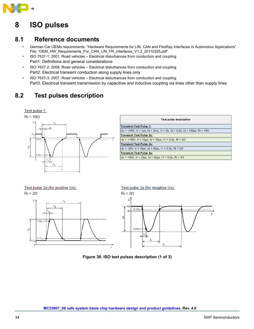
8.2 Test pulses description
Figure 36. ISO test pulses description (1 of 3)
Transient Test Pulse 1:
Us = -100V, tr = 1µs, td = 2ms, t1 = 5s, t2 = 0.2s, t3 = 100µs, Ri = 10O
Transient Test Pulse 2a:
Us = +100V, tr = 10µs, td = 50µs, t1 = 0.2s, Ri = 2O
Transient Test Pulse 2a:
Us = -30V, tr = 10µs, td = 50µs, t1 = 0.5s, Ri = 2O
Transient Test Pulse 2a:
Us = +30V, tr = 10µs, td = 50µs, t1 = 0.5s, Ri = 2O
Test pulse description

MC33907_08 safe system basis chip hardware design and product guidelines, Rev. 4.0
NXP Semiconductors 35
ISO pulses
Figure 37. ISO test pulses description (2 of 3)
Transient Test Pulse 2b:Us = +10V, tr = 1ms, td = 0.2s, t6 = 1ms, t12 = 1ms, Ri = 0.05�Transient Test Pulse 3a:Us = -150V, tr � 5ns, td = 100ns, t1 = 100μs, t4 = 10ms, t5 = 90ms, Ri = 50�Transient Test Pulse 3b:Us = +100V, tr � 5ns, td = 100ns, t1 = 100μs, t4 = 10ms, t5 = 90ms, Ri = 50�
Test pulse description
U
UA
US
t12
tr
td
t6 t
0,9 US
0,1 UA 0,1 US
0,9 UA
0
Test Pulse 2b:Ri - 0.05Ω

MC33907_08 safe system basis chip hardware design and product guidelines, Rev. 4.0
36 NXP Semiconductors
ISO pulses
Figure 38. ISO test pulses description (3 of 3)
Transient Test Pulse 4 (crank):
VBAT= UB = 12V, Us = 6.9V, Ua = 5V, t10 = 5ms, t7 = 40ms,
t8 = 50ms, t9 = 20s, t11 = 5ms … 100ms, Ri = 0.01O
Transient Test Pulse 4 (crank):
VBAT= UB = 12V, Us = 8.8V, Ua = 7V, t10 = 5ms, t7 = 40ms,
t8 = 50ms, t9 = 20s, t11 = 5ms … 100ms, Ri = 0.01O
Transient Test Pulse 5b (load dump):
Us = 87V (ext. Clamp = 40V), tr = 5ms ... 10ms, td = 400ms, Ri = 0.5O
Test pulse description

MC33907_08 safe system basis chip hardware design and product guidelines, Rev. 4.0
NXP Semiconductors 37
ISO pulses
8.3 ISO pulse schematic
Figure 39. ISO pulse schematic
External componentsfrom the proposal list
MC33907_08 safe system basis chip hardware design and product guidelines, Rev. 4.0
38 NXP Semiconductors
ISO pulses
8.4 Product setup
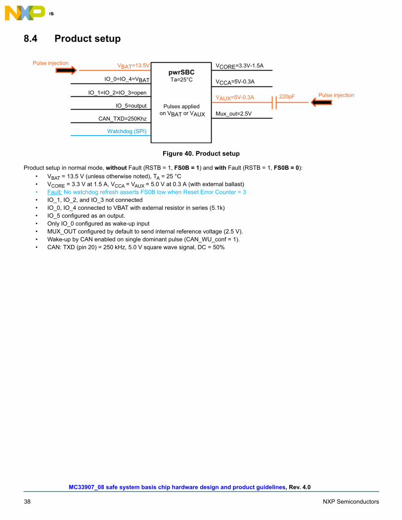
Figure 40. Product setup
Product setup in normal mode, without Fault (RSTB = 1, FS0B = 1) and with Fault (RSTB = 1, FS0B = 0):
• VBAT = 13.5 V (unless otherwise noted), TA = 25 °C• VCORE = 3.3 V at 1.5 A, VCCA = VAUX = 5.0 V at 0.3 A (with external ballast)• Fault: No watchdog refresh asserts FS0B low when Reset Error Counter = 3• IO_1, IO_2, and IO_3 not connected• IO_0, IO_4 connected to VBAT with external resistor in series (5.1k)• IO_5 configured as an output.• Only IO_0 configured as wake-up input • MUX_OUT configured by default to send internal reference voltage (2.5 V).• Wake-up by CAN enabled on single dominant pulse (CAN_WU_conf = 1). • CAN: TXD (pin 20) = 250 kHz, 5.0 V square wave signal, DC = 50%
VBAT=13.5V VCORE=3.3V-1.5A
VCCA=5V-0.3A
VAUX=5V-0.3A
Mux_out=2.5V
IO_0=IO_4=VBAT
IO_1=IO_2=IO_3=open
IO_5=output
CAN_TXD=250Khz
pwrSBCTa=25°C
Pulses appliedon VBAT or VAUX
220pF
Watchdog (SPI)
Pulse injection
Pulse injection

MC33907_08 safe system basis chip hardware design and product guidelines, Rev. 4.0
NXP Semiconductors 39
ISO pulses
8.5 Results
8.6 Failing criteria
8.6.1 Class A without fault (RSTB = 1, FS0B = 1)• Monitoring of supply voltages: VCORE (3.3 V) ±3%, VCCA (5.0 V) ±3%, VAUX (5.0 V) ±3%, VCAN (5.0 V) ±5%• Monitoring of internal reference voltage (on MUX_OUT pin): 2.5 V ±1%• RXD (CAN) follows TXD (pin 20) with amplitude within 5.0 V ±0.9 V, and jitter ±10%• No active reset means no RSTB latched during 10 ms (default init FSSM1 register configuration)• No activation of FS0B• No SPI configuration change (init. registers)• No diag and status register change
8.6.2 Class A with fault (RSTB = 1, FS0B = 0)• Monitoring of supply voltages: VCORE (3.3 V) ±3%, VCCA (5.0 V) ±3%, VAUX (5.0 V) ±3%, VCAN (5.0 V) ±5%• Monitoring of internal reference voltage (on MUX_OUT pin): 2.5 V ±1%• RXD (CAN) follows TXD (pin 20) with amplitude within 5.0 V ±0.9 V, and jitter ±10%• Fault still reported (FS0B = 0)• No Diag and status register change
Applied on Pulse typeNb of pulse or
test timePulse description and product setup Class
Transient Test Pulse 1 ‐ buck boost CTransient Test Pulse 1 ‐ buck only CTransient Test Pulse 2a (+100 V) ‐ buck boost BTransient Test Pulse 2a (+100 V) ‐ buck only BTransient Test Pulse 2a (+30 V) ‐ buck boost ATransient Test Pulse 2a (+30 V) ‐ buck only ATransient Test Pulse 2a (‐30 V) ‐ buck boost ATransient Test Pulse 2a (‐30 V) ‐ buck only ATransient Test Pulse 2b ‐ buck boost CTransient Test Pulse 2b ‐ buck only CTransient Test Pulse 3a ‐ buck boost ATransient Test Pulse 3a ‐ buck only ATransient Test Pulse 3b ‐ buck boost ATransient Test Pulse 3b ‐ buck only ATransient Test Pulse 4 (Vmin=2.7 V) ‐ buck boost C*Transient Test Pulse 4 (Vmin=2.7 V) ‐ buck only CTransient Test Pulse 4 (Vmin=4.6 V) ‐ buck boost ATransient Test Pulse 4 (Vmin=4.6 V) ‐ buck only C**Transient Test Pulse 5 ‐ buck boost BTransient Test Pulse 5 ‐ buck only BTransient Test Pulse 3a ‐ buck boost ATransient Test Pulse 3a ‐ buck only ATransient Test Pulse 3b ‐ buck boost ATransient Test Pulse 3b ‐ buck only A
* full load condition on all regulators as detailed in the setup slide** VCCA and VAUX configured at 5.0 V
Vaux10 mn
10 mn
Pulse 3a
Pulse 3b
Vbat
5000Pulse 1
Pulse 2b
Pulse 2a
Pulse 5
5000
500
5000
10 mn
10 mn
5
10Pulse 4
Pulse 3b
Pulse 3a

MC33907_08 safe system basis chip hardware design and product guidelines, Rev. 4.0
40 NXP Semiconductors
ISO pulses
8.6.3 Class B without fault (RSTB = 1, FS0B = 1)• All functions return automatically to within normal limits after exposure is removed • One or more of the supply or reference voltages can go beyond specified tolerances • RXD (CAN) pin can go beyond specified tolerances • No active reset means no RSTB latched during 10 ms (default init FSSM1 register configuration)• No activation of FS0B • No SPI configuration change (init. registers) • No Diag and status register change
8.6.4 Class B with fault (RSTB = 1, FS0B = 0)• All functions return automatically to within normal limits after exposure is removed • One or more of the supply or reference voltages can go beyond specified tolerances • RXD (CAN) pin can go beyond specified tolerances • Fault still reported (FS0B = 0)• No Diag and status register change
8.6.5 Class C without fault (RSTB = 1, FS0B = 1)• All functions return automatically to within normal limits after exposure is removed • Reset RSTB occurs with or without activation of FS0b
8.6.6 Class C with fault (RSTB = 1, FS0B = 0)• All functions return automatically to within normal limits after exposure is removed • One or more of fault outputs have changed (RSTB = 0 or FS0B = 1)
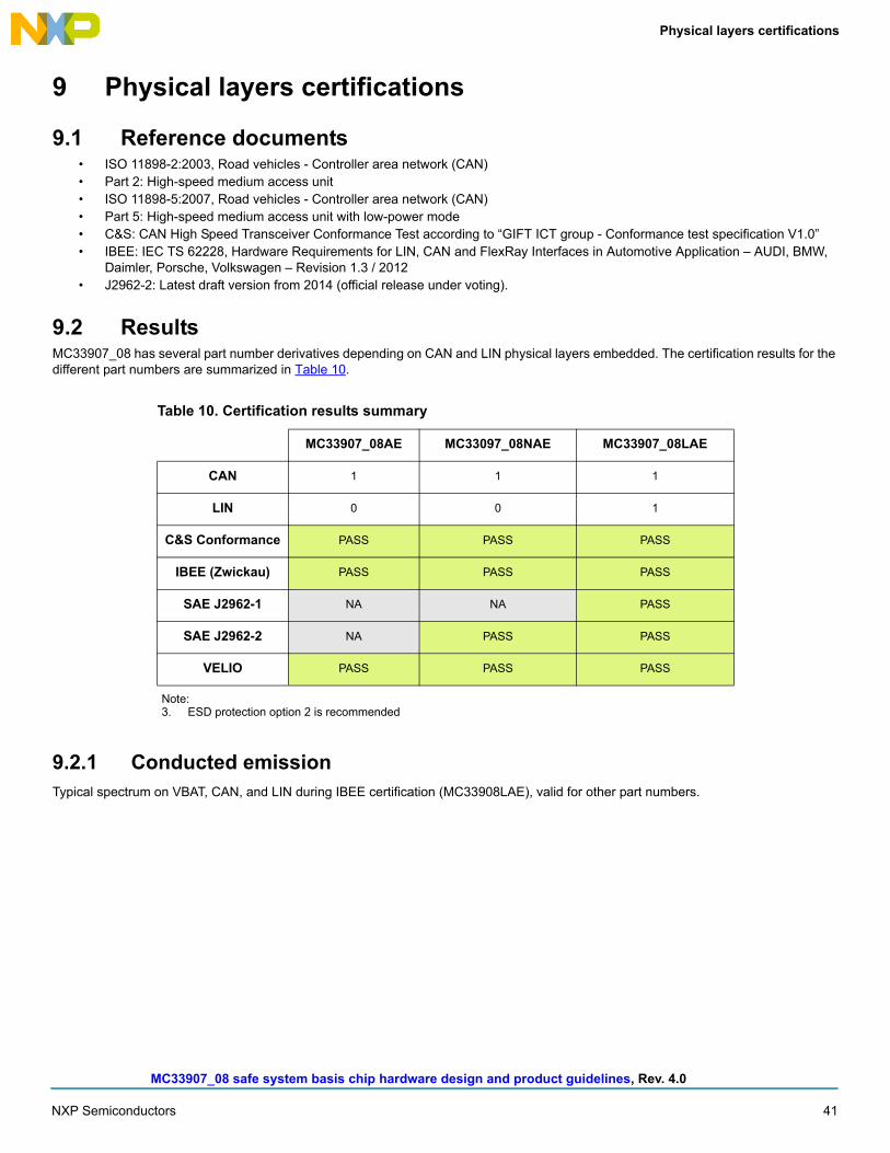
MC33907_08 safe system basis chip hardware design and product guidelines, Rev. 4.0
NXP Semiconductors 41
Physical layers certifications
9 Physical layers certifications
9.1 Reference documents• ISO 11898-2:2003, Road vehicles - Controller area network (CAN)• Part 2: High-speed medium access unit• ISO 11898-5:2007, Road vehicles - Controller area network (CAN)• Part 5: High-speed medium access unit with low-power mode• C&S: CAN High Speed Transceiver Conformance Test according to “GIFT ICT group - Conformance test specification V1.0”• IBEE: IEC TS 62228, Hardware Requirements for LIN, CAN and FlexRay Interfaces in Automotive Application – AUDI, BMW,
Daimler, Porsche, Volkswagen – Revision 1.3 / 2012• J2962-2: Latest draft version from 2014 (official release under voting).
9.2 ResultsMC33907_08 has several part number derivatives depending on CAN and LIN physical layers embedded. The certification results for the different part numbers are summarized in Table 10.
9.2.1 Conducted emissionTypical spectrum on VBAT, CAN, and LIN during IBEE certification (MC33908LAE), valid for other part numbers.
Table 10. Certification results summary
MC33907_08AE MC33097_08NAE MC33907_08LAE
CAN 1 1 1
LIN 0 0 1
C&S Conformance PASS PASS PASS
IBEE (Zwickau) PASS PASS PASS
SAE J2962-1 NA NA PASS
SAE J2962-2 NA PASS PASS
VELIO PASS PASS PASS
Note:3. ESD protection option 2 is recommended

MC33907_08 safe system basis chip hardware design and product guidelines, Rev. 4.0
42 NXP Semiconductors
Physical layers certifications
Figure 41. Conducted emission on VBAT
Figure 42. Conducted emission on the CAN Bus
Emission Measurement global pinsTransceiver: MC33908LAETest Case: Emission VBAT (#3)Mode / measuring: normal / CP3 (VBAT)Bus filter: without
[dBμV]80
70
60
50
40
30
20
10
-10
0
0,1 1 10 100 1000[MHz]
Emission VBAT- normal mode
noise
OEM Requirement
TS1 @C / TS3 @C
Emission Measurement CANTransceiver: MC33908LAETest Case: Emission LIN (#1f)Mode / measuring: normal / CP1 (CAN )Bus filter: 100μH CMC
[dBμV]80
70
60
50
40
30
20
10
-10
0
0,1 1 10 100 1000[MHz]
Emission CAN- normal mode
noise
OEM Requirement
TS1 @C / TS3 @C
TS2 @C / TS3 @C

MC33907_08 safe system basis chip hardware design and product guidelines, Rev. 4.0
43 NXP Semiconductors
Physical layers certifications
Figure 43. Conducted emission on LIN Bus
9.2.2 SAE J2962-2 option 2 description
Figure 44. CAN ESD protection - option 2
Table 11. CAN ESD protection component list
Option No. Component name Label Value
2Capacitor C3, C4 82 pF, 100 V ±5% (1)
Zener D2, D3 NXP PESD1CAN, (in same SOT23 package)
Note1. Over entire voltage and temperature operating range
Emission Measurement LINTransceiver: MC33908LAETest Case: Emission LIN (#2f)Mode / measuring: normal / CP2 (LIN)Bus filter: 3 x 68pF
[dBμV]80
70
60
50
40
30
20
10
-10
0
0,1 1 10 100 1000[MHz]
noise
OEM Requirement
TS1 @C / TS3 @C
Emission LIN- normal mode
+ VDD

MC33907_08 safe system basis chip hardware design and product guidelines, Rev. 4.0
44 NXP Semiconductors
References
10 ReferencesThe following are URLs where you can obtain information on related NXP products and application solutions:
NXP.com Support Pages
Description URL
MC33907_8Power System Basis Chip with High Speed CAN Transceiver
http://www.nxp.com/files/analog/doc/data_sheet/MC33907_8.pdf
MC33907-MC33908D2Power System Basis Chip with High Speed CAN and LIN Transceivers
http://www.nxp.com/files/analog/doc/data_sheet/MC33907-MC33908D2.pdf
MC34FS6407-08Power System Basis Chip with High Speed CAN Transceiver
http://www.nxp.com/files/analog/doc/data_sheet/MC34FS6407-08.pdf
AN4661Designing the VCORE Compensation Network For The MC33907/MC33908 System Basis Chips
http://www.nxp.com/files/analog/doc/app_note/AN4661.pdf
AN4442Integrating the MPC5643L and MC33907/08 for Safety Applications
http://www.nxp.com/files/32bit/doc/app_note/AN4442.pdf
AN4388 Quad Flat Package (QFP) http://www.nxp.com/files/analog/doc/app_note/AN4388.pdf
AN4843Low-Power Wireless Charging Using the NXP WCT1001A Controller
http://www.nxp.com/files/microcontrollers/doc/app_note/AN4843.pdf
AN5099Integrating the MPC5744P and MC33907/08 for Safety Applications
http://www.nxp.com/files/microcontrollers/doc/app_note/AN5099.pdf
MC33907-MC33908PDTCALC
MC33907/8 Power Dissipation Toolhttp://www.nxp.com/webapp/sps/site/prod_summary.jsp?code=MC33908&tab=Design_Tools_Tab
Vcore compensation network simulation tool Upon demand
Non ISO pulses report Upon demand
FMEDA MC33907/8 FMEDA Upon demand
MC33907_8SMUG MC33907/8AE Safety Manual https://www.nxp.com/webapp/Download?colCode=MC33907_8SMUG
MC33907_8NLSMUG MC33907/8NAE, MC33907/8LAE Safety Manualhttps://www.nxp.com/webapp/Download?colCode=MC33907NL-MC33908NLSMUG
KIT33908AEEVB Evaluation Board http://www.nxp.com/webapp/sps/site/prod_summary.jsp?code=KIT33908AEEVB
KIT33908LAEEVB Evaluation Board http://www.nxp.com/webapp/sps/site/prod_summary.jsp?code=KIT33908LAEEVB
KIT33908MBEVBE Evaluation Mother Board (EVM)http://www.nxp.com/webapp/sps/site/prod_summary.jsp?code=KIT33908MBEVBE
KITMPC5643DBEVM Evaluation Daughter Board (Qorivva MPC5643L)http://www.nxp.com/webapp/sps/site/prod_summary.jsp?code=KITMPC5643DBEVM
KITMPC5744DBEVMEvaluation Daughter Board (Qorivva MPC5744P)
http://www.nxp.com/webapp/sps/site/prod_summary.jsp?code=KITMPC5744DBEVM
MC33907 Product Summary Page http://www.nxp.com/webapp/sps/site/prod_summary.jsp?code=MC33907
MC33908 Product Summary Page http://www.nxp.com/webapp/sps/site/prod_summary.jsp?code=MC33908
Analog Home Page http://www.nxp.com/analog
MC33907_08 safe system basis chip hardware design and product guidelines, Rev. 4.0
45 NXP Semiconductors
Revision history
11 Revision history
Revision Date Description
1.0 1/2014 • Initial release
2.0 3/2015
• Major updates • Added MC33907_8NL supported part numbers • Added CAN and LIN physical layers certification results • Added SMPS components calculation/selection method • Added Layout example • Added ISO pulses • Improved overall descriptions • Updated graphics to conform with NXP standards
3.0 8/2015
• Updated J2962 certification results • Updated VBAT input filter requirement for J2962 • Added Simplified Internal Power Tree • Added VSENSE accuracy improvement chapter • Added IO wake-up chapter • Added Section 6.3, MC33907 attach to Infineon Aurix MCU, page 28 • Added Section 6.4, MC34FS6407_08 derivatives from MC33907_08, page 28
4.0 3/2016
• Updated Figure 1 • Updated with NXP external components references • Corrected Debug Mode Entry Figure 25 (Dbg_Rpd resistor was not visible) • Added chapter 5.4.3 Reduce Vaux_PNP Power Dissipation • Added chapter 5.4.4 VAUX Supplying a Sensor • Added chapter 5.8 MC33907_08 Basic Start up Sequence • Updated form and style

Information in this document is provided solely to enable system and software implementers to use NXP products.
There are no expressed or implied copyright licenses granted hereunder to design or fabricate any integrated circuits
based on the information in this document. NXP reserves the right to make changes without further notice to any
products herein.
NXP makes no warranty, representation, or guarantee regarding the suitability of its products for any particular
purpose, nor does NXP assume any liability arising out of the application or use of any product or circuit, and
specifically disclaims any and all liability, including without limitation, consequential or incidental damages. "Typical"
parameters that may be provided in NXP data sheets and/or specifications can and do vary in different applications,
and actual performance may vary over time. All operating parameters, including "typicals," must be validated for each
customer application by the customer's technical experts. NXP does not convey any license under its patent rights nor
the rights of others. NXP sells products pursuant to standard terms and conditions of sale, which can be found at the
following address:
http://www.nxp.com/terms-of-use.html.
How to Reach Us:
Home Page: NXP.com
Web Support: http://www.nxp.com/support
NXP, the NXP logo, Freescale, the Freescale logo, the Energy Efficient Solutions logo, SafeAssure, the SafeAssure
logo and SMARTMOS are trademarks of NXP B.V. All other product or service names are the property of their
respective owners. All rights reserved.
© 2016 NXP B.V.
Document Number: AN4766Rev. 4.0
3/2016