Embed Size (px)
Citation preview
PoS(TIPP2014)020
Development of a Technological Prototype ofSilicon-Tungsten Electromagnetic Calorimeter forILD
Vincent Boudry∗ on behalf of the ILD SiW-ECAL development groupLaboratoire Leprince-Ringuet - École polytechnique, CNRS/IN2P3Palaiseau, F-91128 FranceE-mail: [email protected]
The specific conditions of the International Linear Collider offer perfect conditions to use im-proved reconstruction techniques, based on Particle Flow Algorithms. They require Highly Gran-ular Calorimeters. Recent advances in Monte-Carlo simulation, integrated electronics, large com-posite structures associated with the power-pulsed working mode of the collider allow for high-density, triggerless, almost dead-zone free calorimeters. The R&D efforts concerning the Silicon-Tungsten option of the ILD experiment near the ILC will be here summarised.
Technology and Instrumentation in Particle Physics 2014,2-6 June, 2014Amsterdam, the Netherlands
∗Speaker.
© Copyright owned by the author(s) under the terms of the Creative Commons Attribution-NonCommercial-ShareAlike Licence. http://pos.sissa.it/
PoS(TIPP2014)020
R&D SiW-ECAL for ILD Vincent Boudry
1. Introduction
1.1 ILC & ILD
The International Linear Collider (ILC) is an electron-positron accelerator whose construc-tion is nowadays being envisaged in the North of Japan. Despite high centre of mass energies(250− 500GeV in stages, upgradable to 1TeV) and high luminosity (0.8− 3 · 1034 cm−2s−1), theenvironment is relatively background free. The main one – pair production – being easily canalisedin the beam pipe by a high magnetic field. As the beams will be pulsed at 5Hz in short trains of1300−2600 bunches with a comfortable separation (350−700ns for a total length of 1ms), it wasdecided to develop high-granularity calorimeters integrating a fully embedded readout electronicswith local zero-suppression, local storage and delayed readout. To avoid thermal dissipation itshould run in power-pulsed mode, with a typical duty cycle of 1%.
1.2 Constraints on the detectors
The typical physics channels exploited, be they Higgs or top quark production, will generatejets of energies between 40 and 100GeV. As a touchstone for performance evaluation of variousdetectors and reconstruction software options, the separation of events with pairs of WW and ZZwas selected. In practise, a single Jet Energy Resolution (JER) of σ(Ejet)/Ejet . 3.8% is required.This about a twice a good as the performance reached with the LEP detectors [1].
One innovative way to achieve this goal is to use the Particle Flow Algorithms (PFA) [2], inwhich every particle in a jet is individually reconstructed and measured using the best informationavailable: tracks for charges particles (65% in energy of a typically jet), ECAL for the photons(25%), and the calorimeters for the neutral hadrons, h0(10%). Using the complete PFA frameworkPandoraPFA [3], it has been demonstrated [4] on fully simulated data samples that this goal can beobtained using:
• a state-of-the-art TPC with a resolution of δPT/PT ∼ 5 ·10−5PT,
• a precision vertex detector (σx,y,z ∼ 10µm) and
• Electromagnetic and Hadronic Calorimeters (ECAL and HCAL) with average single particleresolution (σEγ/Eγ ∼ 16%/
√Eγ and σEh0/Eh0 ∼ 50%/
√Eh0).
This requires in turn to separated the contributions of individual particles in calorimeters, makingthem imaging or highly granular devices.
1.3 Imaging Calorimetry
With nowadays technology a 1000 fold increase in granularity w.r.t. current standard calorime-ters (such as e.g. the ones in the LHC experiments). A gain by a factor of two in JER w.r.t. to purecalorimetric measurement has been obtained. Advanced software techniques might allow to evengo further (see the contribution by N. v. d. Kolk at this conference).
Practical imaging calorimetry in a full size detector such as the ILD brings many challengescombining:
• Mechanics to provide modular self-supporting structure with minimal dead materials, defor-mations and non-homogeneity;
2
PoS(TIPP2014)020
R&D SiW-ECAL for ILD Vincent Boudry
• (Micro-)Electronics to provide reliable low-noise, low-power Very Front End (VFE) readoutchips (ROC) fully embedded in the detectors, over large surfaces;
• Instrumentation to provide high quality, yet not too expensive, sensors;
• Thermics for the proper self-cooling of the devices.
The entanglement of those aspects requires an iterative procedure of prototype building, testing andimprovement, with a constant vigilance on physics performances, cost, quality and industrialisationissues. Last but not least the performances can only be assessed using PFA algorithms, and are assuch a non-trivial combination of hardware and reconstruction software.
1.4 The Si-W ECAL of ILD
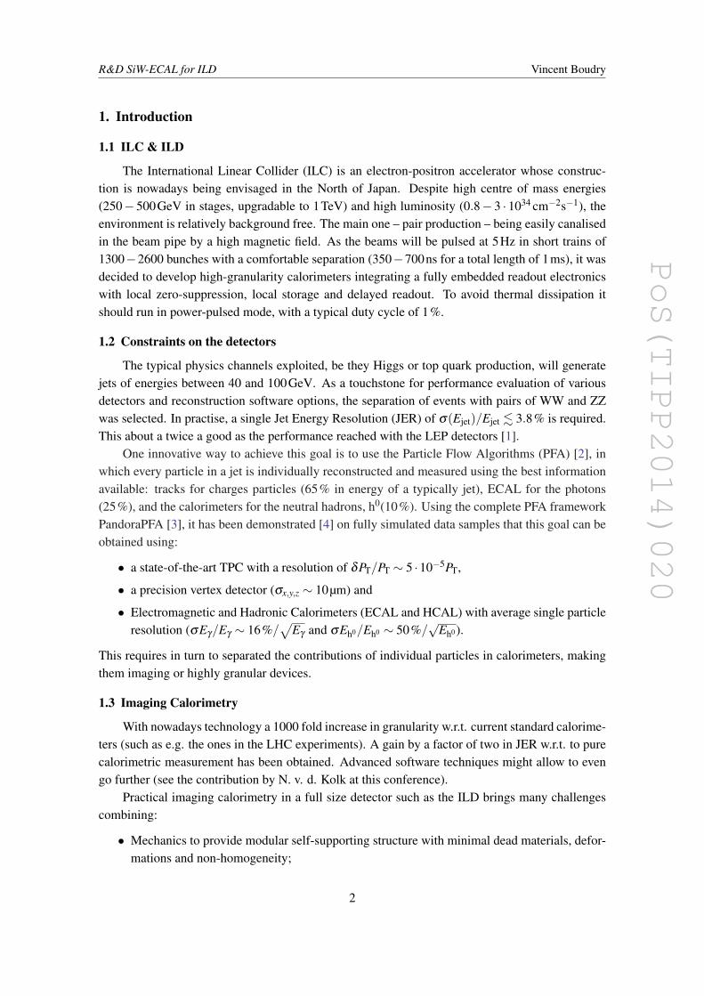
The CALICE collaboration1 main purpose is to foster the R&D on imaging calorimeters, bysharing experience and means to develop and test prototypes and techniques. Among various op-tions kept for the ECAL of the ILD experiment, the Silicon-Tungsten ECAL (SiW-ECAL) is themost compact and advanced one. It features large highly-resistive Silicon PIN diodes, finely seg-mented (5×5mm2), directly glued on PCB’s holding the ROC. The PCB’s are stitched together byglued flat connectors. Sided by a Kapton film carrying the High Voltage (HV) on one side and bya Copper thermal drain on the other side, they are assembled on both sides of an H-shaped supportholder composed of a Tungsten core wrapped in a carbon fibres. Such a structure is dubbed a SLAB.Up to 15 SLAB’s (for 30 sensitive layers) will be inserted in a large (140−180×90×30cm3) com-posite Tungsten-Carbon Fibre structure, ensuring a total of 24 X0.
Figure 1: Structure of the ECAL in ILD (Left); Holding structure of the SiW-ECAL in the barrel (right).
1.5 The Prototypes of Si-W ECAL
A so-called physical prototype was build in 2005, and extensively tested in beam test campaignuntil 2011. This device strongly inspired the PAMELA satelite [5].
A second prototype is being build; as a technological test-stand, it will fully integrate anembbeded electronics, using the SKIROC2 analogue/digital ASIC [6, 7] featuring auto-triggering,a 14-bit signal dynamics, partial zero suppression, a memory for 15 events and power-pulsing for64 channels. The pixel size will be ∼ 5.5× 5.5mm2 inside a tower of 15 single layered SLAB’s.One of the SLAB will be a long one to test the readout over large surfaces, wile all the other ones
1https://twiki.cern.ch/twiki/bin/view/CALICE/WebHome
3
PoS(TIPP2014)020
R&D SiW-ECAL for ILD Vincent Boudry
will be instrumented only over a surface of 18× 18cm2. Beside the validation of the techniquesused, its building will also help to establish procedures and develop preliminary semi-automatedtest benches for mass production.
Among all the aspects addressed by the technological prototype, recent advances were reachedin Thermic & Mechanical studies, in the preparation of the assembly of elements, in the Siliconwafer optimisation and finally on the optimisation of global parameters. Those 4 items will bedescribed in this article. The Acquisition and VFE Electronics aspects are detailed in F. Gastaldiand Ch. de la Taille contributions to these proceedings.
2. Thermal & Mechanical studies
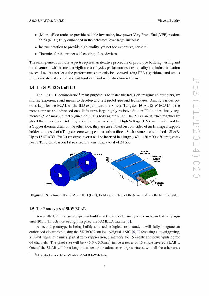
Barrel structure model: A complete prismatic composite Tungsten–Carbon fibre structure sim-ilar to the one designed for the barrel of ILD has been realised in December 2011. It features 3rows of 15 alveoli (see fig. 2). The last 5 are thicker to accommodate SLAB’s with a double amountof Tungsten (4.2mm) w.r.t. the first 10 SLAB’s (2.1mm). The same amount of Tungsten is foundbetween the alveoli in the two sections.
Its dimensions (55.2×149.1×20.5cm3) and weight (∼ 700kg) are close to the ones of the ILD(between 60% to 95% depending on the final dimensions). The building process has been fromthe start-on designed for industrialisation: the Carbon-Fibre alveoli are produced with a singledimension, then cut to fit in the mould and assembled with the Tungsten plates in an autoclaveunder vacuum. This structure will be used as a support for the technological prototype to be testedin beams.
Figure 2: Structure for the ECAL prototype with a stack of short SLAB’s (left); CAD design of barrelstructure with the FBG (right).
Metrology: Some of the alveoli and the structure have been equipped with Fibre Bragg-Grated(FBG) to measure their deformations. The deformation of the single alveolus under transversalstress has been properly reproduced by finite element analysis (FEA). The metrology using 3Dmeasuring arm machine (FARO) of the structure has show a small deformation (max: 5.28mm) atthe centre of the upper part of the structure. This point will have to be improved for final production.
ILD ECAL: In ILD the ECAL barrel has the form of a solid octagonal cylinder. The 8 stavesare composed of 5 modules, hold by 3 rails onto the HCAL. Each modules (corresponding to oneTungsten-Carbon structure) contains 5 towers of 15 SLAB’s (equipped with Scintillator or Silicon
4
PoS(TIPP2014)020
R&D SiW-ECAL for ILD Vincent Boudry
sensors). In the current design (as described in [8]) its internal radius is Rmin. = 1808mm, itsexternal one Rmax. = 2020mm for a half-length of Zhalf = 2348mm. These numbers might bereduced by 20 to 30% after optimisation, as well as the number of towers and layers. ExtensiveFEA calculus have shown a maximum deformation of the loaded structure below 0.1mm. The
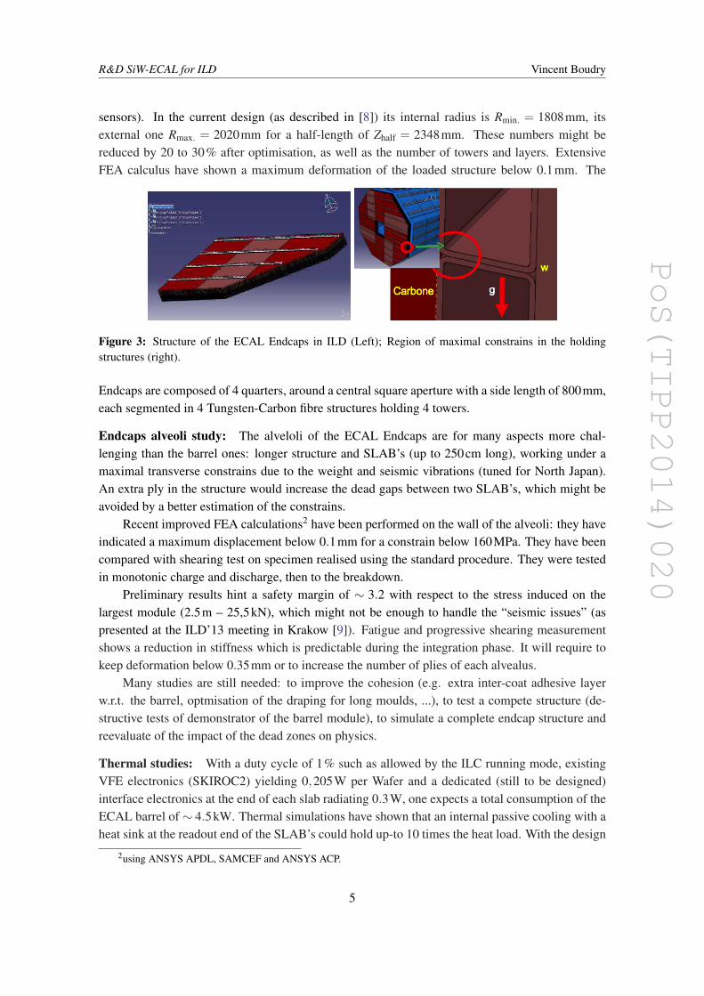
Figure 3: Structure of the ECAL Endcaps in ILD (Left); Region of maximal constrains in the holdingstructures (right).
Endcaps are composed of 4 quarters, around a central square aperture with a side length of 800mm,each segmented in 4 Tungsten-Carbon fibre structures holding 4 towers.
Endcaps alveoli study: The alveloli of the ECAL Endcaps are for many aspects more chal-lenging than the barrel ones: longer structure and SLAB’s (up to 250cm long), working under amaximal transverse constrains due to the weight and seismic vibrations (tuned for North Japan).An extra ply in the structure would increase the dead gaps between two SLAB’s, which might beavoided by a better estimation of the constrains.
Recent improved FEA calculations2 have been performed on the wall of the alveoli: they haveindicated a maximum displacement below 0.1mm for a constrain below 160MPa. They have beencompared with shearing test on specimen realised using the standard procedure. They were testedin monotonic charge and discharge, then to the breakdown.
Preliminary results hint a safety margin of ∼ 3.2 with respect to the stress induced on thelargest module (2.5m – 25,5kN), which might not be enough to handle the “seismic issues” (aspresented at the ILD’13 meeting in Krakow [9]). Fatigue and progressive shearing measurementshows a reduction in stiffness which is predictable during the integration phase. It will require tokeep deformation below 0.35mm or to increase the number of plies of each alvealus.
Many studies are still needed: to improve the cohesion (e.g. extra inter-coat adhesive layerw.r.t. the barrel, optmisation of the draping for long moulds, ...), to test a compete structure (de-structive tests of demonstrator of the barrel module), to simulate a complete endcap structure andreevaluate of the impact of the dead zones on physics.
Thermal studies: With a duty cycle of 1% such as allowed by the ILC running mode, existingVFE electronics (SKIROC2) yielding 0,205W per Wafer and a dedicated (still to be designed)interface electronics at the end of each slab radiating 0.3W, one expects a total consumption of theECAL barrel of ∼ 4.5kW. Thermal simulations have shown that an internal passive cooling with aheat sink at the readout end of the SLAB’s could hold up-to 10 times the heat load. With the design
2using ANSYS APDL, SAMCEF and ANSYS ACP.
5
PoS(TIPP2014)020
R&D SiW-ECAL for ILD Vincent Boudry
close to the current one, an isolated ECAL barrel module would experience a thermal gradient of∆T = 2.2 C and an Endcap module of ∆T = 6 C.
3. Assembly: Quality tests & preparation of large production
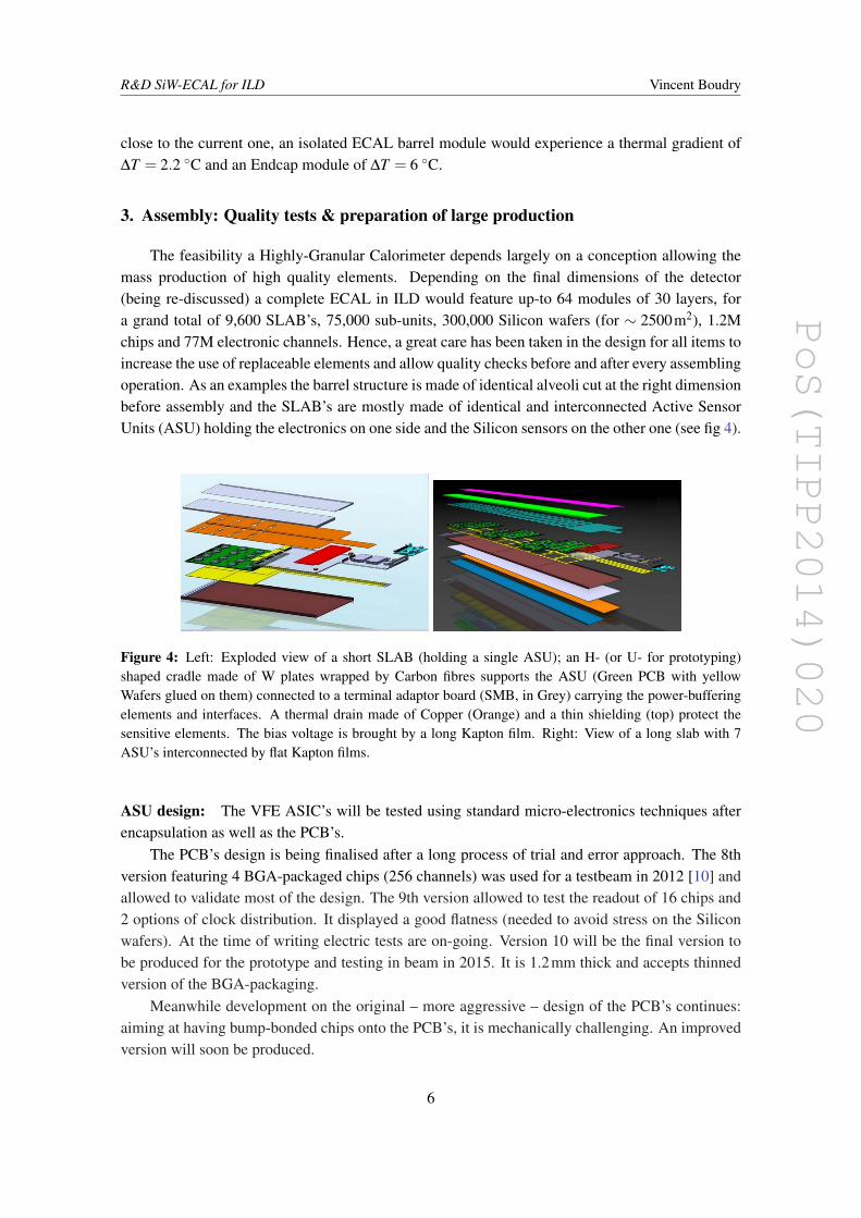
The feasibility a Highly-Granular Calorimeter depends largely on a conception allowing themass production of high quality elements. Depending on the final dimensions of the detector(being re-discussed) a complete ECAL in ILD would feature up-to 64 modules of 30 layers, fora grand total of 9,600 SLAB’s, 75,000 sub-units, 300,000 Silicon wafers (for ∼ 2500m2), 1.2Mchips and 77M electronic channels. Hence, a great care has been taken in the design for all items toincrease the use of replaceable elements and allow quality checks before and after every assemblingoperation. As an examples the barrel structure is made of identical alveoli cut at the right dimensionbefore assembly and the SLAB’s are mostly made of identical and interconnected Active SensorUnits (ASU) holding the electronics on one side and the Silicon sensors on the other one (see fig 4).
Figure 4: Left: Exploded view of a short SLAB (holding a single ASU); an H- (or U- for prototyping)shaped cradle made of W plates wrapped by Carbon fibres supports the ASU (Green PCB with yellowWafers glued on them) connected to a terminal adaptor board (SMB, in Grey) carrying the power-bufferingelements and interfaces. A thermal drain made of Copper (Orange) and a thin shielding (top) protect thesensitive elements. The bias voltage is brought by a long Kapton film. Right: View of a long slab with 7ASU’s interconnected by flat Kapton films.
ASU design: The VFE ASIC’s will be tested using standard micro-electronics techniques afterencapsulation as well as the PCB’s.
The PCB’s design is being finalised after a long process of trial and error approach. The 8thversion featuring 4 BGA-packaged chips (256 channels) was used for a testbeam in 2012 [10] andallowed to validate most of the design. The 9th version allowed to test the readout of 16 chips and2 options of clock distribution. It displayed a good flatness (needed to avoid stress on the Siliconwafers). At the time of writing electric tests are on-going. Version 10 will be the final version tobe produced for the prototype and testing in beam in 2015. It is 1.2mm thick and accepts thinnedversion of the BGA-packaging.
Meanwhile development on the original – more aggressive – design of the PCB’s continues:aiming at having bump-bonded chips onto the PCB’s, it is mechanically challenging. An improvedversion will soon be produced.
6
PoS(TIPP2014)020
R&D SiW-ECAL for ILD Vincent Boudry
The interconnection format to other ASU’s and to the adaptor board has been thoroughlytested. It was verified that in a strong magnetic field (2T) the power-pulsing operation had nosignificant effect on the contact resistivity [11].
ASU test bench: A versatile test-bench has been realised which allows to validate a completePCB (1024 channels) with or without Silicon wafers. A PVC platform holding a SMB card con-nected to the DAQ system is extruded to leave space optionally for a HV Kapton film and wafers, athick PMMA3 fastening up to 1024 test probes using calibrated springs, and shielding. The PCB to-be-tested comes on top in contact with the array of springs, with a monitored force. It is connectedto the SMB by mechanical contacts.
The device has been designed to serve as well as a R&D station, as a basis for the qualificationof the PCB for the prototype and as basis for later mass-test bench for the ILD-ECAL.
Gluing station: The gluing of 4 wafers onto a PCB is done by depositing calibrated dots ofconductive glue on every readout pad. It is a complex process which involves the global and localflatness of the board, for the correct estimation of the amount of glue needed. The parallelism ofthe edges conditions the positioning of the wafers (the goal is ∼ 100µm).
After a semi-automated positioning and gluing tested on the ASU’s used for the 2012 beamtests, the gained experience translated into improvement on the use of specific pumps for a dry andclean vacuum, on cleaning of the PCB and a differentiated positioning of the glue dots at the edgeof the PCB to prevent short-cuts. A fully automated chain combining the dot deposition and waferpositioning is under conception, to be completed by a readout test bench to characterise the newlyformed ASU’s.
Assembly Bench: Finally the ASU’s have to be assembled into full SLAB’s. The developmentof a set of specifications to assure proper assembly of ASU’s (Tolerances of PCB, H or U cra-dle) is being defined: as an example mechanical stress on wafers during interconnections is beeninvestigated.
Two stations are being investigated: one for the interconnection, the second for the assembly.They will be be combined and automatised.
4. Wafers
The silicon sensors, high resistivity (3− 4kΩm) PIN diodes, are the basis unit the ECAL:in term of total cost (for about one half), but primarily for its dimension, so as to maximise theyield of square wafers drawn from cylindrical ingots4. The sensors are segmented in an arrayof cells, with dimension ranging from 10× 10mm2 for the physical prototype to 5.5× 5.5mm2
for the technological prototype. The size and number of cells is adjusted to the dimension of thewafer and the capacity of the readout ASIC’s. The “Guard Rings” (GR) are structures implementednear the edge of the sensors to gradually dampen the bias voltage and avoid leakage currents (orbreakdown) through the defects of the edges. It was discovered during the beam test of the physical
3Poly(methyl methacrylate)4Whereas an hexagonal shape would optimise this yield, a square shape is preferable in terms of mechanics, reduc-
tion of dead space and mass production of the components.
7
PoS(TIPP2014)020
R&D SiW-ECAL for ILD Vincent Boudry
prototype of the ECAL with high energy electrons, that a percent coupling between the guard ringand the readout cells resulted in so-called “square events”, in which all the peripheral cells wereresponding.
An R&D program [12] is on-going on the GR aiming at reducing the peripheral dead-zone,limiting its coupling to external cells, and provide a non-proprietary techniques to open-up thewafer-producer park. The use of segmented GR to reduce the capacitive coupling and of “edge-less” techniques are investigated. These studies are mainly done in the scope of the French-ANR5
program CALIIMAX in relation with Kyushu U. and Hamamatsu (HPK) as well as with variousEuropean producers.
Recently a batch of sensors without GR, thanks to laser edging, and slightly higher resistivitywas provided by Hamamatsu. The dimensions and layout (surface of 90× 90mm2 segmented in256 cells of 5.5×5.5mm2 for a thickness of 320µm) are identical to the old one. Capacity-Voltages(C-V) curves show a lower bias voltage (30V vs. 65V) needed to stabilise the capacitance. FromIntensity-Voltage (I-V) measurements, reduced absolute leakage currents (31nA vs. 48nA for120V bias voltage were found. Thanks to earlier stabilisation a lower bias voltage could be used,yielding leaking current of 21nA at 60V. More details can be found on Tatsuhiko Tomita’s posterat this conference.
Several designs of segmented GR have been realised and implemented on so-called babywafers (∼ 3× 3cm2 segmented in an array of 3× 3 cells). To test the coupling of the GR withthe border cells, charges are injected in the bulk in a corner of the wafer with the help of a pulsedNd:YAG laser (1064nm, 1.5ns) focused on a 20µm spot. The cells are readout by a dedicatedDAQ system. Whereas for 1 GR design, the signal more or less scales with the length of the outerrim of the cells (i.e. corner cells receive twice as much as side cells, except for the cell opposite tothe injection spot), the segmented GR show a very strong relative reduction of coupling. A futurebatch of baby wafer will feature meshed electrodes on the pixels (now fully metallised), so as toallow charge injection – and calibration – inside a pixel.
A second laser test bench is now available with similar characteristics (wavelength of 1056nm,1ns pulse width) injecting the equivalent of 700 MIP. It is mounted on a flexible test bench allowingthe readout of a free standard-sized wafer connected by an array of springs to a prototype PCB andacquisition. Preliminary results show a coupling between 0.4 to 0.5% for side cells. It scales withthe length of the rim: doubled for corner cells and double-sized ones, quadrupled for double-sizedcorners ones. The system will be improved to reduce noise and PCB bending (preventing now allchannels to be connected).
5. Issues & near future:
The DESY test beam of the current set-up allowed to demonstrate an excellent potential, e.gthat a signal/noise ratio (MPV of MIP signal / noise dispersion) of up-to 14 is feasible. It was alsovery useful to reveal several issues: frequent post-triggering of the ASIC’s, some noisy channels,lack of external triggering, a small non-linearity. The charge injection on test bench also showedsome dispersion of the signal w.r.t. the memory depth in the ASIC’s. All these effects are now
5French National Research Agency, Grant ANR-2010-0429-01
8
PoS(TIPP2014)020
R&D SiW-ECAL for ILD Vincent Boudry
understood and will be solved or improved by the next version of the PCB’s, either by changingthe routing or better decoupling.
The technological prototype will be completed in 2015 and tested that year with high energybeams.
6. Acknowledgements
This work has been supported by the CNRS-IN2P3, the JSPS, the French ANR, grant agre-ment CALIIMAX-HEP ANR-2010-0429-01, and from the European Commission under the FP7Research Infrastructures project AIDA, grant agreement no. 262025.
References
[1] H. Videau and J. C. Brient, “Calorimetry optimised for jets,” in Proc. 10th International Conferenceon Calorimetry in High Energy Physics (CALOR 2002), Pasadena, California. March, 2002.
[2] J. C. Brient, “Improving the jet reconstruction with the particle flow method: An introduction,” inCalorimetry in particle physics. Proceedings, 11th International Conference, CALOR 2004, Perugia,Italy, March 29-April 2, 2004, pp. 445–451. 2004.
[3] M. A. Thomson, “Particle Flow Calorimetry and the PandoraPFA Algorithm,” Nucl. Instrum. Meth.A611 (2009) 25–40, arXiv:0907.3577 [physics.ins-det].
[4] ILD Concept Group Linear Collider Collaboration, T. Abe et al., “The International LargeDetector: Letter of Intent,” tech. rep., FERMILAB / DESY/ KEK, 2010. arXiv:1006.3396[hep-ex].
[5] M. Boezio, V. Bonvicini, E. Mocchiutti, P. Schiavon, G. Scian, et al., “A High granularity imagingcalorimeter for cosmic ray physics,” Nucl.Instrum.Meth. A487 (2002) 407–422,arXiv:physics/0109010 [physics].
[6] S. Callier, F. Dulucq, C. de La Taille, G. Martin-Chassard, and N. Seguin-Moreau, “SKIROC2, frontend chip designed to readout the Electromagnetic CALorimeter at the ILC,” JINST 6 (2011) C12040.
[7] CALICE and EUDET Collaboration, C. de La Taille, “Performance of 2nd generationCALICE/EUDET ASICs,” in Proceedings of 14th International Conference on Calorimetry in HighEnergy Physics (CALOR 2010), Beijing, China. 10-14 May 2010., vol. 293, p. 012016. 2011.
[8] ILD Collaboration, T. Behnke et al., “International Linear Collider – Detector Baseline Document,”tech. rep., DESY / FERMILAB / CERN, 2013. http://edmsdirect.desy.de/edmsdirect/file.jsp?edmsid=D00000001021295&fileClass=native;. in print;Draft in http://www.linearcollider.org/ILC/physics-detectors/Detectors/Detailed-Baseline-Design.
[9] https://agenda.linearcollider.org/conferenceDisplay.py?confId=6113.
[10] T. Frisson et al., “Beam test performance of the SKIROC2 ASIC,” CALICE Internal Note submittedto Nucl.Instrum.Meth. A (2014) . https://twiki.cern.ch/twiki/pub/CALICE/CaliceInternalNotes/CIN-023.pdf.
[11] N. Seguin-Moreau, “Interconnection tests in magnetic field.”https://agenda.linearcollider.org/getFile.py/access?contribId=50&
sessionId=9&resId=0&materialId=slides&confId=5947.
[12] CALICE Collaboration, R. Cornat, “Front-end Electronics for the CALICE/EUDET Calorimeters,”2009. arXiv:0901.4849 [physics.ins-det].
9