Embed Size (px)
Citation preview

DIELECTRIC SPECTROSCOPY OF VERY LOW LOSS MODEL POWER CABLES
Thesis submitted for the degree of
Doctor of Philosophy
at the University of Leicester
by
Tong Liu, MSc, BSc
Department of Engineering
University of Leicester
February 2010

DIELECTRIC SPECTROSCOPY OF VERY LOW LOSS MODEL POWER CABLES
by
Tong Liu
Abstract
This research study focuses on the dielectric response of XLPE model power cables that have combinations of homo- and co-polymer insulation with furnace and acetylene carbon black semicon shields. Three dielectric spectroscopy techniques, which are frequency response analyzer and transformer ratio bridge in both frequency domain, and charging/discharging current system in time domain, were jointly used to measure the low loss XLPE cables in the frequency range from 10-4Hz to 104Hz at temperatures from 20°C to 80°C. Degassing effects and thermal ageing effects have also been studied with the spectroscopy techniques. Thermal-electric behaviour and maximum voltages for thermal breakdown have been theoretically simulated for the model cables.
Three loss origins of the XLPE cables have been found with different loss mechanisms. Conduction loss due to thermally activated electron/hole hopping dominates the lower frequency range from 10-4Hz to 1Hz; Semicon loss due to its in series resistance with the insulation layer in cable equivalent circuit dominates the higher frequency range from 102Hz to 104Hz; intrinsic polarization loss of the XLPE insulation has dominant flat loss spectra in the mid-frequency range from 1Hz to 102Hz. Degassing was found to decrease the conductivity of the model cables, while thermal ageing greatly increased the conductivity. Thermal-electric simulation results with FEMLAB have shown that the position of maximum field changes from inner to outer insulation boundary under higher applied voltages. A loss mechanism model with mathematical expression for dielectric loss spectrum calculation is finally proposed to explain the total dielectric loss of polymer power cables.

Acknowledgements
I am greatly thankful to my supervisor, Professor John Fothergill, for his helps,
inspirations and encouragement on my study and life. His broad knowledge, hard-
working attitude, optimistic character, generous mind and kind heart towards all the
other people have impressed and moved me. He has fundamentally changed me during
my three years in Leicester. I feel lucky to be a student of such a great person.
I also sincerely thank my co-supervisor, Dr Stephen Dodd, for his excellent guidance.
His expertise always helped me to choose the best solution for lots of problems in my
study. He is extremely serious and passionate to scientific research, which makes me
feel hungry for knowledge. I would not have done a good research if not him.
I wish to thank Dr Mingli Fu for all his enormous supports and kind helps on both my
study and my life all along the way. He is my benefactor.
I would like to thank Dr Paul Lefley for his precious advice on my first year and second
year report which formed a good basis for my PhD thesis.
Besides, Professor Len Dissado, Andy Willby, Alan Wales, Nikola Chalashkanov,
Abdelghaffar Abdelmalik and Antonios Tzimas all gave me many helps. They are the
ones of many people I would like to thank in the Engineering Department.
Especially, this is also a chance to express my thanks to Borealis AB for its sponsorship
and Mr Ulf Nilsson for all his kind helps on my research.
Finally, I must thank my family. My parents gave me unconditional support on my PhD
study. My wife sacrificed herself to support me while taking care of our daughter. I will
try my best to give my family happy life.

Contents 1 Introduction............................................................................................................... 1 2 Literature review....................................................................................................... 7
2.1 Background knowledge .................................................................................... 7 2.2 Dielectric properties of insulation materials ................................................... 12
2.2.1 Polarization of dielectric materials ............................................................. 12 2.2.2 Dielectric loss and conduction in dielectrics .............................................. 18 2.2.3 The Debye model of dielectric relaxation and its modifications ................ 21 2.2.4 Equivalent circuit analysis .......................................................................... 25
2.3 Cable insulation materials............................................................................... 30 2.3.1 Materials of cable insulation layer.............................................................. 30 2.3.2 Materials of semiconducting layer.............................................................. 33 2.3.3 Degradation and breakdown of XLPE cable insulation.............................. 35
2.4 Electrical conduction in polymeric materials ................................................. 39 2.4.1 Conduction mechanisms of bulk insulation................................................ 40 2.4.2 Conduction mechanisms due to electrode charge injection........................ 43
2.5 Dielectric spectroscopy techniques ............................................................. 45 2.5.1 Time domain dielectric spectroscopy ..................................................... 46 2.5.2 Bridge techniques ....................................................................................... 50 2.5.3 Frequency response analyzer technique ..................................................... 53
3 Characterizing the dielectric response of power cables.......................................... 56 3.1 Sample preparation of model power cables.................................................... 56
3.1.1 Introduction to model power cables............................................................ 56 3.1.2 Sample preparation ..................................................................................... 58
3.2 Choice and development of techniques for low loss measurement ................ 61 3.2.1 Frequency response analyzer in the range from 10-4Hz to 1Hz.................. 61 3.2.2 Transformer ratio bridge in the range from 300Hz to 10kHz..................... 75 3.2.3 Time domain charging/discharging current technique in the range from 1Hz to 250Hz.................................................................................................................. 81
3.3 Experimental procedures .............................................................................. 105 3.3.1 Degassing and ageing of the model cables ............................................... 105 3.3.2 Experimental plan on different XLPE model cables ................................ 107
3.4 Conclusions................................................................................................... 109 4 Dielectric response analysis of model power cables ............................................ 111
4.1 Dielectric response at low frequencies of from 10-4Hz to 1Hz..................... 111 4.1.1 Thermal expansion calibration.................................................................. 111 4.1.2 Temperature dependent dielectric loss ..................................................... 115 4.1.3 Comparison of different model cables...................................................... 118
4.2 Dielectric loss in the higher frequency range of from 300Hz to 10kHz....... 120 4.2.1 Loss tangent measurement results on different model cables................... 120 4.2.2 The loss origins due to semicon shields.................................................... 123 4.2.3 MATLAB modelling of dielectric response of the power cables ............. 126
4.3 Dielectric response with discharging current measurement ......................... 133 4.3.1 Temperature dependent discharging current of different cables .............. 133 4.3.2 Transformation of discharging current into frequency spectra................. 137
4.4 Master curve in the frequency range from 10-4Hz to 104Hz......................... 144 4.4.1 Data combination of different techniques................................................. 144

4.4.2 Loss tangent master curves ....................................................................... 153 4.5 Effect of degassing by conduction current measurement ............................. 156
4.5.1 Time delay for conduction measurement.................................................. 156 4.5.2 Results of non-degassed, air degassed and vacuum degassed cables ....... 157
4.6 Conclusions................................................................................................... 162 5 Thermal ageing effects on model power cables.................................................... 163
5.1 Dielectric response of aged model power cables using FRA ....................... 164 5.1.1 Ageing effect on homo-polymer model power cables.............................. 164 5.1.2 Ageing effect on co-polymer model power cables ................................... 166
5.2 Discharging current of aged model power cables......................................... 169 5.3 The loss tangent spectra from 10-4Hz to 102Hz ............................................ 173 5.4 Ageing effects on conductivity of model power cables................................ 176
5.4.1 Influence of thermal ageing on conductivity of model power cables....... 176 5.4.2 Activation energy change after thermal ageing ........................................ 178
5.5 Dielectric loss measurement using Schering bridge ..................................... 181 5.5.1 Measurement system and sample preparation .......................................... 181 5.5.2 Measurement results ................................................................................. 184
5.6 Conclusions................................................................................................... 188 6 Thermal breakdown simulation on model power cables ...................................... 189
6.1 Introduction................................................................................................... 189 6.2 Mathematical model of thermal-electric behaviour for power cables .......... 191 6.3 Thermal breakdown simulation setup in FEMLAB ..................................... 198 6.4 Simulation results of model power cables .................................................... 205
6.4.1 MTV without load current at different ambient temperatures.................. 205 6.4.2 MTV with heat injection due to load current............................................ 215
6.5 Conclusions................................................................................................... 219 7 Discussion............................................................................................................. 220
7.1 Summary of experimental results on the model power cables ..................... 220 7.2 Conduction loss of cable insulation .............................................................. 222 7.3 Resistive loss of semicon layers ................................................................... 227 7.4 Polarization loss of XLPE insulation............................................................ 232 7.5 Dielectric loss model for XLPE power cables.............................................. 236
8 Conclusions and Further Work ............................................................................. 242 9 References............................................................................................................. 247 Appendix A: Meetings and publications ...................................................................... 262

1
1 Introduction
A power cable is an assembly used for transmission of electrical power. In power
systems, power cables are used all through the network in power plants, substations,
high voltage transmission lines, and mains lines. They are installed everywhere as
permanent wiring within buildings, buried in the ground, run overhead, or exposed.
Like blood vessels of human bodies, power cables are critical components of power
systems. The research, development and application of power cables are important for
the performance and reliability of power transmission. High voltages carried by power
cables are insulated by dielectric materials. Nowadays the insulation systems of power
cables need to withstand extra high voltages with reliable long-term operation and
insulation thickness as thin as possible. Any insulation defects of power cables can
cause power failure, which subsequently result in economic loss including power cut
cost, compensation cost, replacement cost and health/safety cost. Therefore, the study
on the insulation system of power cables has great benefit to the cable manufacturing
industry.
The oil-paper insulated power cable was invented by Ferranti in 1891 [1] and used for a
long time without fundamental changes in the basic cable insulation system until the
early 1960s, when polymeric insulation, predominantly polyethylene (PE), cross-linked
polyethylene (XLPE) and ethylene propylene rubber (EPR), was introduced [2]. There
has been enormous technical improvement based on the research of high voltage
engineering and insulation dielectrics to minimise defects, such as voids and conducting
impurities.

2
Because of the intrinsic breakdown strength of up to 800kV/mm and enhanced
operating temperature from 75°C to 90°C after cross linking [3], XLPE cables are the
best choice and dominating in power industry nowadays. The typical structure of XLPE
cables is shown in Figure 1.1. The conductor is insulated by the XLPE insulation layer,
which is sandwiched by two semiconductive screen layers. This comprises the basis of a
power cable. Metallic shielding and outer covering layers are used for further protection.
Over the past 30 years XLPE cable system failure rates have dramatically decreased
even though the voltage stress per millimeter of insulation has continuously increased.
500kV power cables have been already developed for more than 10 years with an
insulation thickness of 27mm [4] [5]. However, with more and more demanding
requirements for the insulation systems of power cables, XLPE cables are still subject to
further improvements. It has problems such as dielectric energy loss due to
polarization/relaxation and ionic conduction, appearance of water and/or electrical trees,
which are normally found after long term operating.
Figure 1.1 Typical structure of XLPE power cables
As a consequence, insulation ageing and failure have been widely studied for the
reliable operation and safety of power equipment for many years. As one of the most
popular and powerful research techniques, dielectric spectroscopy is playing a main role

3
in both ageing and fault detection for insulation systems including power cables.
Dielectric spectroscopy is a technique to study the interaction of a material and the
applied electric field. In particular, dielectric loss mechanisms which lead to energy
dissipation and ageing of the insulation material are studied under variable frequency
AC conditions and stepped DC conditions. Although there are various techniques for
dielectric spectroscopy studies, including frequency and time domain measurements, the
dielectric loss measurement of XLPE cables is beyond the abilities of many commercial
instruments due to the following facts:
1. XLPE theoretically contains only very weak polar molecular groups and is
without a net permanent dipole. As a consequence, XLPE has a very low
dielectric constant and very low energy dissipation factor.
2. Commercial XLPE and subsequent thermal conditioning results in a material
with low levels of impurities and additives which can contribute to electrical
conductivity and dielectric loss.
3. XLPE cables have much thicker insulation than typical film samples used for
dielectric spectroscopy. For a given value of applied voltage, the higher electric
field that will exist within film samples make their dielectric properties easier to
measure.
Film samples cannot represent the insulation system of power cables, although they will
make more sensitive measurements of the dielectric properties. It is not possible to
study the loss mechanisms of power cables with measurement on film samples due to
the following reasons:
4
1. The formation of crystalline structures, which are known as lamella, are
influenced by thermal history and manufacturing methods. This makes the
morphological characteristics of thin films different from the bulk insulation
layer of XLPE cables.
2. Unlike film samples, the insulation system of power cables includes
semiconducting layers, which are carbon black filled polymers and used to
smooth the electric field between central/outer conductors and insulation layer.
The semiconducting layers have relatively smaller resistance with unique
dielectric properties and may contribute to dielectric loss of power cables.
3. The cross linking by-products and impurities greatly influence the dielectric
properties of XLPE material. The concentration and distribution of these
insulation defects inside power cables which are produced by extrusion
manufacturing process is different from film samples.
In order to study the dielectric properties of power cables more accurately, model cables
with the same composition and manufacturing process can be used. The model cables
should have extrusion production as actual cables comprising of inner conductor, inner
semiconducting layer, polymer insulation and outer semiconducting layer. They should
also have thinner insulation layer enabling higher electric fields to be applied. The
investigation on these model cables can provide more useful and accurate information
on the dielectric properties and loss mechanisms, which are important for studying the
ageing and breakdown of power cables.
The purpose of this research project is to study the origins of dielectric loss in XLPE
power cables using XLPE model cables manufactured by Borealis AB. These model

5
cables are extruded cables with a central conductor surrounded by an inner
semiconducting layer, primary XLPE insulation and an outer semiconducting layer. The
base materials for both semiconducting layers and primary insulation can be altered to
assess the influence of the dielectric loss mechanisms by different materials and
combinations. The model cables are studied by means of both frequency dielectric
spectroscopy (FDDS) and time domain dielectric spectroscopy (TDDS), in order to
determine the loss mechanisms of the power cables with broad dielectric spectra. As
XLPE has very low dielectric loss, different techniques and measurement instruments
are surveyed in order to resolve the dielectric loss over a wide range of frequency from
10-4Hz to 104Hz. Different spectroscopy techniques such as frequency response
analyzer, transformer ratio bridges and electrometers have different capabilities and
sensitivities over a fixed range of frequencies and applied voltage. Hence, dielectric
spectroscopy techniques that are capable of resolving the very low loss XLPE cables
must be identified and developed. In addition, sensitive measurements of current are
also required to measure the low level of electrical conductivity of the insulation as this
will also contribute to electrical power loss within the cable. With these novel
techniques, different types of XLPE model cables, which have different insulation layer
and semiconducting layer materials, will be measured for comparison and identification
of the loss mechanisms that could lead to ageing of the cable and subsequent failure.
The results of this work will, therefore, provide cable manufacturers relevance in
reducing power dissipation within high voltage cables and improve the reliability of
cable designs. Equivalent circuit simulations of XLPE cables incorporating the various
loss mechanisms, modelling of thermal runaway and microscopic investigation of the
cable insulation will be complementary activities in order to aid interpretation of the

6
dielectric response and provide predictive models for cable ageing that can be scaled up
to production cables.
In this thesis, chapter 2 contains the research background information from literature
survey and introduction of relevant theories, knowledge and techniques that are
important and fundamental for this research study. Chapter 3 introduces the exploration
of appropriate spectroscopy techniques for low loss power cable measurement in both
time and frequency domains. Chapter 4 discusses the dielectric loss spectra of three
different techniques and the master curves in a wide frequency range from 10-4Hz to
104Hz. The degassing effects of the model XLPE cables are also studied in this chapter.
Chapter 5 includes the thermal ageing effects of the model power cables. The field
dependent measurement on both aged and unaged cable samples using Schering bridge
at 50Hz is shown in this chapter. In chapter 6, the thermal-electric behaviour and
maximum voltage for thermal breakdown of the model cables is studied, based on the
previous conductivity measurement results. Chapter 7 discusses the dielectric origins
and possible loss mechanisms of the XLPE power cables. Conclusions and proposed
further work are in the last chapter 8.

7
2 Literature review
2.1 Background knowledge
A dielectric or insulation material is a non-conducting substance, i.e. an insulator. The
term was coined by Whewell [6] in response to a request from Faraday. Dielectric
materials can be solids, liquids, or gases and have a variety of applications in power
industry. The use of electrical insulation is as old as the science and technology of
electrical phenomena, and systematic investigations of dielectric properties may also be
traced back to 1870’s. After Debye’s theory on ideally non-interactive molecular dipole
model of dielectrics, numerous monographs have been done by scientists from different
aspects of view to understand dielectric materials. Theory of Dielectrics [7] provides an
insight into the mathematical origins of dielectric behaviours. After long history of
evolution, more practical and recent studies by A. K. Jonscher [8] [9] are emphasizing
on the solid dielectrics and trying to establish a universal law based on all the
experimental works so far. Other scientists, i.e. Daniel [10] and Hill et al.. [11], also
contributed greatly to the understanding of dielectric theories with many approaches. As
far as the polymeric insulation materials are concerned, L.A. Dissado and J.C. Fothergill
have intensively investigated the mechanisms of degradation and breakdown of
polymers, based on decades of research work on polymer insulation materials [12].
Since the application of polymeric cables came into use, the insulation systems of
power cables have been studied worldwide, mainly on XLPE cables, in order to
improve their reliability and performance. The dielectric loss mechanism study on
power cables are mainly experimental investigation, with the dielectric science
theoretical foundations. While it is a cross linked scientific area of electrical engineering

8
and material science, many practical techniques play a role in the study, typically
dielectric spectroscopy of this research, space charge measurement popularly by PEA
method, thermally stimulated depolarisation current (TSDC) measurement and scanning
electron microscopy (SEM). John Densley [13] proposed an overview on multi-factor
ageing mechanisms and list of diagnostic techniques for power cables including paper-
insulated lead covered cables (PILC), self-contained fluid-filled (SCFF) cables, XLPE
and ethylene propylene rubber (EPR) cables. John Fothergill [14] has led the European
“HVDC” project to explore diagnostic techniques for HV XLPE cables based on
electrical, micro-structural, physical and chemical characterization with lots of
cooperated experimental work in UK, France and Italy. Space charge accumulation and
behaviour in the cable insulation have been investigated recent years, especially on
HVDC cables. Fabiani and Montanari et al. [15] [16] [17] have published series feature
articles on polymeric cable design and space charge accumulation, following the
enormous work by other people’s previous studies on XLPE power cables [18] [19] [20]
[21] [22]. Recently, the semiconducting shields and their interfaces with the insulation
layers of power cables raised focus while it was found that the defects of power cables
are generally in these areas. Kegerise in Okonite company and Person in Dow Chemical
company have studied the influence of cable semiconducting shields on cable dielectric
losses and proposed dome manufacturing and performance criteria [23] [24]. The
degradation of XLPE cables due to the semiconducting protrusion during production
will initiate electrical trees by lightning and switching surges, as Bamji has found [25].
Tanaka [26] studied the facilitation of oriented lamellar growth at the interface by
addition of special ingredients to the semiconducting layer, in order to improve the
interfaces between shields and insulation. The role of degassing in XLPE power cables
was studied and reviewed in joined effort of international companies by people of T.

9
Andrews (NEETRAC, Georgia Tech, USA), A. Smedberg (Borealis AB, Sweden), V.
Waschk (NKT Cables, Germany) and W. Weissenberg (Brugg Cables, Switzerland)
[27]. They concluded that degassing contributes greatly to the quality of power cables
by improving the certainty in electrical testing and improving the dielectric properties.
As the most important factor for XLPE cable failures, water trees have been studied by
measuring the cable’s relative permittivity and conduction with equivalent circuit under
different voltages [28]. Thermal ageing effects of XLPE cables were also studied by
Boubakeur [29], while thermo-luminescence in XLPE cable insulation was measured by
Bamji and Bulinski [30]. Besides lots of research work on XLPE cables, a comparison
of thermal and mechanical properties of EPR and XLPE cable compounds was
introduced by Xiaoguang Qi [31].
Dielectric spectroscopy has a long history application on the research of dielectric
materials, but not until recent years has it been used for the study and diagnostics of
power equipment. Primary use of dielectric spectrometer includes some dielectric
organic materials which were measured to study their polarization behaviour [32] or
find out the property change due to ageing phenomenon [33]. Later on, more and more
applications on power equipment test helped the development of novel insulation
materials [34] [35] [36]. Time domain dielectric spectroscopy, which includes DC
conduction measurement, also has lots of global application on various practical
materials such as LDPE, HDPE, XLPE [37] [38] [39], epoxy [40], polyimide-Teflon
[41], polyethyleneterephthalate [42] and holmium oxide [43]. Together with space
charge and TSDC measurement, the charging/discharging current can provide
polarization details inside the materials and frequency spectra by Fourier transform or
Hammon approximation. In addition to the basic theories of solid dielectrics, Walter S.
Zaengl has summarized the basic theoretical features of dielectric spectroscopy in both

10
time and frequency domain for HV power equipment [44] and introduced several
applications on power transformers and different types of power cables in his following
feature article [2]. New spectroscopic measurement techniques have also been improved
to be more sensitive, precise and automatic for low loss dielectric materials [45] [46]
[47].
Research on dielectric spectroscopy of XLPE power cables does not have a long history,
though studies on various engineering materials including polymers began as early as
the application of these kinds of materials. Dielectric spectroscopy can be classified into
frequency domain techniques and time domain techniques. As far as the dielectric loss
of power cables is concerned, frequency dependent spectroscopy is commonly used and
particularly favoured by industrial research, probably because of the commercial
availability of frequency response analyzers by GE, Novocontrol and Solartron [48] and
other bridge-based high sensitivity instruments for power frequency test such as
Schering Bridge. The research group at the Royal Institute of Technology in Sweden,
cooperating with ABB Corporate Research, spent several years developing an
impedance analyzer based on high voltage dielectric spectroscopy system for XLPE
power cables [49] [50] and some direct experimental results up to 100Hz were obtained
[51] [52] [53] [54]. General Electric Company is also concerned with the dielectric
spectroscopy as a condition assessment for XLPE and PILC (paper insulated lead
covered) cables by their frequency domain measuring equipment IDA 200 [55].
Together with SINTEF Energy Research in Norway, ABB Corporate Research finished
a joint project on condition assessment of 12kV and 24kV XLPE cables using frequency
response analyzer and found that a correlation between the voltage level and breakdown
voltage of the cable [56]. Although the frequency range of frequency domain dielectric
spectroscopy on XLPE cables and other power equipment is generally below 1kHz,

11
high frequency range spectroscopy using Fourier transform infrared spectroscopy has
also been done by KIM Chonung from 70kHz~10MHz [57]. Because of the nonlinearity
of polyethylene material under different levels of AC voltages, which is explained by
Jean Crine [58], the frequency domain method has difficulty to detect nonlinear
phenomenon, although it is the most popular and widely used technique. Due to the
limitation of frequency domain dielectric spectroscopy of linear assumption and indirect
DC conduction measurement, time domain dielectric spectroscopy, specifically
polarization/depolarization or charging/discharging current measurement technique and
return voltage measurement method, is complementary and can provide the same
information on the materials [2] [44] [59]. While there exist no commercial instrument
of time domain technique due to difficulties in low level measurement precision and
proper explanation of acquired information, especially for the low loss polymeric XLPE
cables, charging/discharging current measurement has been used as a laboratory
research tool. The transient current measurement for water tree detecting in polymeric
cables has been studied by Li et al. [60]. The influence of time window size on
frequency spectra was theoretically analyzed and charging/discharging currents of
LDPE samples are measured. The temperature, pressure and field dependence of
anomalous discharging currents in XLPE films have been investigated by Malec et al.
[61]. They concluded that the blocking by electrodes and mobility of both charge
carriers play an important role in the discharging behaviour of XLPE samples, and the
conclusion support the suggestion that the time domain discharging current in
polyethylene are caused by the movement of space charge built up during charging time.
As time domain dielectric spectroscopy techniques are becoming mature, proposal work
of online diagnostic application on XLPE power cables has been done by National
Research Council of Canada using depolarization current measurement [62] [63].

12
Following the continuous efforts of commercialization for time domain spectroscopy,
very recently an instrument, AVO Megger S1-5010 with up to 5kV 2% accuracy and
0.1nA detection limit, was used for condition assessment of XLPE cables by
polarization/depolarization current with 1s interval [64].
Individual dielectric spectroscopy technique in either frequency or time domain is no
longer sufficient to reveal the status of cable insulation, hence more and more
researchers in recent years are studying both time and frequency domain spectroscopy
[59] [65]. Correlations and combination of the different techniques on critical materials
such as polyethylene and epoxy or insulation systems such as transformers’ oil-paper
insulation and rotating machine’s stator bars have already yielded valuable knowledge
on condition assessment, diagnostics and development of power equipments [66] [67]
[68] [69] [70] [71], among which XLPE cables attract many researchers [72] [73] [74].
Thanks to the persistent efforts of all dielectric scientists, the measurement techniques
on power equipment are being improved and understanding of solid polymeric materials
of practical importance is gradually being gained, although there are still difficulties and
challenges, especially for very low loss materials and insulation systems of typically
XLPE cables.
2.2 Dielectric properties of insulation materials
2.2.1 Polarization of dielectric materials
When a uniform static electric field E is applied on a plate capacitor with vacuum
medium between the electrodes, according to Coulomb’s law,
EQ 0ε= Equation 2-1

13
where 0ε is the free space permittivity with the value 8.85×10⁻¹² F/m. The capacitance
of the vacuum plate capacitor
VQC =0 Equation 2-2
If a dielectric material is inserted between the electrodes, as shown in Figure 2.1 with
solid line connection of DC voltage application, the material will respond to the applied
electric field by redistributing its component charges to some extent. Positive charges
will be attracted towards the negative electrode and vice versa. This effect is called
polarization of the material [75].
Figure 2.1 Polarization of dielectric material between plate electrodes
If the material is isotropic, certain amount of dipoles will be produced, aligning in the
field direction inside the material. Thus, the polarization P is defined as a vector
quantity of the magnitude and direction of the electric moment per unit volume in the
material by the applied field. The polarization with bound charges makes more charge
stored on the electrodes and, therefore, the capacitance after inserting the dielectric
medium is increased. The ratio of the increased capacitance C to the vacuum

14
capacitance 0C used to be called dielectric constant and now is more scientifically
named as real part relative permittivity ε ′ ,
χεε
εε +=+=+
=+
==′ 1100
0
0 EP
EPE
QPQ
CC Equation 2-3
where χ is the susceptibility of the material. ε ′ describes the ability of polarization
that occurs in the material and is an important property of dielectric materials,
depending on the frequency of the field applied, humidity, temperature.
In electromagnetism, the electric displacement field D represents how an electric field E
influences the organization of electrical charges in a given medium, including charge
migration and electric dipole reorientation. With the above Equation 2-3 the electric
displacement D in the material can be rearranged as
PEED +=′= 00 εεε Equation 2-4
This is the fundamental electric field equation that applies at any point in an isotropic
medium.
The maximum polarization, corresponding to the highest observable relative
permittivity, will be realised only when sufficient time is allowed after the application
of an electric field. The observed permittivity is static permittivity (dielectric constant)
sε , if ample time is allowed. On the other hand, if the polarization is measured
immediately after the field is applied, allowing no time for dipole orientation, the
instantaneous relative permittivity ∞ε will be observed. Between these two extremes of
time scale there is a dispersion, which could be examined by applying an alternating
electric field E with magnitude 0E and angular frequency ω , across a dielectric

15
material tEE ωcos0= . This will produce polarization, which alternates in direction,
and if the frequency is high enough, the orientation of any dipoles will inevitably lag
behind the applied field. As shown in Figure 2.2, the lag of polarization can be
expressed as a phase lag δ in the electric displacement:
δωδωδω
sin)sin(cos)cos()cos(
00
0
tDtDtDD
+=−=
Equation 2-5
which leads to the definition of two relative permittivities
00
0
00
0 sin and cosE
DE
Dε
δεε
δε =′′=′ Equation 2-6
Figure 2.2 AC losses in a dielectric: (a) circuit diagram, (b) Argand diagram of complex
current-voltage relationship.
At different frequencies, these two quantities are dependent on the lag angle δ , which
represents the molecular behaviour for different dielectrics. They are combined into a
complex relative permittivity )(ωε ∗ for dielectric spectroscopy studies.
)()()( ωεωεωε ′′−′=∗ j Equation 2-7

16
There are a number of different dielectric polarization mechanisms at the molecular or
microscopic level, connected to the way a studied medium reacts to the applied field.
Each dielectric mechanism is centred around its characteristic frequency, which is the
reciprocal of the characteristic time of the process. In general, dielectric polarization
mechanisms can be divided into relaxation and resonance processes. Dielectric
relaxation is the momentary delay in the dielectric constant of a material. This is usually
caused by the delay in molecular polarization with respect to a changing electric field in
a dielectric medium. Dielectric relaxation in changing electric fields could be
considered analogous to hysteresis in changing magnetic fields. Relaxation in general is
a delay or lag in the response of a linear system, and therefore dielectric relaxation is
measured relative to the expected linear steady state (equilibrium) dielectric values.
The most common mechanisms, starting from high frequencies, can be divided into
three main categories (shown in Figure 2.3):
a. Electronic polarization: An electric field will cause a slight displacement of the
electrons of any atom with respect to the positive nucleus. The shift is quite
small because the applied field is usually quite weak relative to the intra-atomic
field at an electron due to the nucleus. Electronic polarization can react to very
high frequencies and is responsible for the refraction of light.
b. Atomic polarization: An electric field can also distort the arrangement of atomic
nuclei in a molecule or lattice. The movement of heavy nuclei is more sluggish
than that of electrons, so that polarization cannot occur at such high frequencies
as electronic polarization, and it is not observed above infra-red frequencies. The
magnitude of atomic polarization is quite small, often only one-tenth of that of

17
electronic polarization, although there are exceptions where a particular mode of
bending produces relatively large departure from the normally symmetric
arrangements of positive and negative centres within the molecule. In ionic
compounds the effect can sometimes be very large.
c. Orientational polarization: Molecules with permanent dipole moments tend to be
aligned by the applied field to give a net polarization in that direction. The rate
of dipolar orientation is highly dependent on molecule-molecule interaction.
Orientation of molecular dipoles can make a contribution which is large but may
be slow to develop to the total polarization of a material in an applied field.
Figure 2.3 Dielectric permittivity spectrum over a wide range of frequencies
d. Low frequency dispersion: In the low frequency range, multiple dielectric loss
behaviour might be present. Conduction mechanism will result in a slope of -1
for the imaginary permittivity, while the real part remains constant when the
polarizability of the material is not changed. This is the most common behaviour
of dielectric material because any dielectrics have certain amount of

18
conductivity. If the real and imaginary part permittivities have the same slopes
between -1 and 0, quasi-DC mechanism is present representing partially mobile
charge carriers gradually moving or hopping to the opposite electrode when the
frequency is lower. In this frequency region, Maxwell-Wagner polarization,
which is the interfacial effect of different materials, is also observable when the
real permittivity has a slope of -2 while the imaginary part has slope of -1.
2.2.2 Dielectric loss and conduction in dielectrics
Materials can be classified according to their permittivity and conductivity. Materials
with a large amount of loss inhibit the propagation of electromagnetic waves. In this
case, generally when
1>>′εω
σ , we consider the material to be a good conductor.
Dielectrics are associated with lossless or low-loss materials, where 1<<′εω
σ [76].
Those that do not fall under either limit are considered to be general media. A perfect
dielectric is a material that has no conductivity, thus exhibiting only a displacement
current. Therefore, it stores and returns electrical energy as if it were an ideal capacitor.
In the case of lossy medium, a practical parameter to quantify the loss of a dielectric
material is the dielectric loss tangent defined by the ratio of imaginary permittivity and
real permittivity,
εεδ′′′
=tan Equation 2-8
As shown in Figure 2.2, the current I which flows in the external circuit after
application of an alternating voltage V can be divided into a capacitive component,
VCiIC εω ′= 0 Equation 2-9

19
which leads the voltage by 90°, and a resistive component,
VCIR εω ′′= 0 Equation 2-10
which is in phase with the voltage. Work can only be done by the latter component, and
the physical meaning of the δtan is defined by:
.leenergy/cyc/cycledissipatedenergy tan ∝
′′′
=εεδ
Equation 2-11
ε ′′ here can be called the dielectric loss factor and the dielectric loss tangent δtan is
usually called dissipation factor.
From the above deduction, the energy loss of an ideal capacitor results from the AC
conductivity, whose difference to DC conduction should be emphasised. The AC
conductivity signifies the movement of fixed charges between specific sites and actually
by various types of polarization behaviour in molecular explanation. DC conductivity,
however, involves the movement of free charges at a steady velocity and is due to any
freely moving charge carriers such as free electrons or ions. It is not possible for any
instrument to distinguish between these two types of conductivity, and in order to do
this task interpretive skills are required during data analysis. When a DC conductance is
present within a dielectric system, the DC response will be seen in addition to the AC
conductivity. DC conductance is frequency independent, as it is equivalent to a resistor
being present in parallel to the dielectric, with the results that the loss slope will be -1 as
shown in Figure 2.3. Thus the measured dielectric loss tangent should be practically:
εωεσε
δ′
+′′= 0tan
DC
Equation 2-12

20
including both polarization loss under AC field and direct current conduction existing at
any frequencies.
Besides these two distinct types of conduction, another typical two types of dielectric
phenomenon are also common, especially in polymeric solid materials, which are the
primary interests of this research study. The charge hopping mechanism described by
Dissado-Hill [77] [78] and Jonscher [9] [79] will also contribute to the measured
conductivity in a dielectric system. This charge hopping conduction, either called low
frequency dispersion (LFD) or quasi-DC (QDC), originates from the presence of
partially mobile charge carriers in the material. It is comparatively easy to distinguish
this response from the above two, as charge hopping is characterised by a corresponding
increase in the real part capacitance as introduced previously. Another interfacial effect
of the dielectric materials that have discontinuity has also been found and studied,
firstly by Maxwell and Wagner. The two phase dielectric system has a different
frequency response, which will be discussed in details later, contributing to the system
energy loss with space charge build-up in the specimen. The Maxwell-Wagner
polarisation is expected at the low frequency range and can shift to quite low
frequencies, if the permittivity of the additive is reduced [80].
This can be concluded as three main types:
a. The polarization current characterises the adjustment of the polarizing species to
a step function field and it must go to zero at infinitely long times. No charges
may leave the dielectric system or enter it from the outside as a result of this
process.

21
b. The steady conduction current, or direct current arises from continuous
movement of free charges across the dielectric material from one electrode to
the other. This current does not change the bonded charge distribution in the
system.
c. At low frequencies, QDC of restricted charge carrier conduction and Maxwell-
Wagner mechanism of interfacial polarization will contribute to the dielectric
loss and conduction in polymeric materials which have complex composition of
different molecular species and combination of different molecules.
2.2.3 The Debye model of dielectric relaxation and its modifications
For a unitary substance, there are several empirical equations to describe the dielectric
relaxation behaviour, based on solid fundamental work by Debye who pioneered the
basic theory of dielectric relaxation behaviour, beginning of a macroscopic treatment of
frequency dependence. This treatment rests on two essential premises: exponential
approach to equilibrium and the applicability of the superposition principle. Debye
relaxation is the dielectric relaxation response of an ideal, non-interacting population of
dipoles to an alternating external electric field. It is usually expressed in the complex
permittivity ∗ε of a medium as a function of the field's frequency ω [81] [82]:
ωτεεωεi+Δ
+= ∞∗
1)(
Equation 2-13
where ∞ε is the permittivity at the high frequency limit, ∞−=Δ εεε s where sε is the
static, low frequency permittivity, and τ is the characteristic relaxation time of the
medium.

22
Havriliak-Negami relaxation is an empirical modification of the Debye relaxation
model, accounting for the asymmetry and broadness of the dielectric dispersion curve.
The model was first used to describe the dielectric relaxation of some polymers, by
adding two exponential parameters to the Debye equation [83] [84]:
βαωτεεωε
))(1()(
i+Δ
+= ∞∗ Equation 2-14
The exponents α and β describe the asymmetry and broadness of the corresponding
spectra. Illustration and comparison of different dielectric relaxation models is shown in
Figure 2.4.
The Cole-Cole equation is a dielectric relaxation model that constitutes a special case of
Havriliak-Negami relaxation when the symmetry parameter (β) is equal to 1 - that is,
when the relaxation peaks are symmetric [85]:
αωτεεωε
)(1)(
i+Δ
+= ∞∗ Equation 2-15
Most polymers show dielectric relaxation patterns that can be accurately modeled by
this equation.
Davidson-Cole model is another model that is a special case of Havriliak-Negami
relaxation, where the broadness parameter 1=α . It improved the fit with experiment by
using a slightly different semi-empirical equation [86]:
βωτεεωε
)1()(
i+Δ
+= ∞∗ Equation 2-16

23
(a) Real permittivity of different models
(a) Imaginary permittivity of different models
Figure 2.4 Illustration of complex permittivity for different models
( ∞ε = εΔ =τ =1, α = β =0.5)

24
This equation corresponds to a skewed distribution of relaxation times about τ , but still
has no particular theoretical foundation apart from the improved agreement with
experiment for certain materials.
For the relaxation models of multiple dielectric materials, such as impurity effect or
interfacial effect between the electrode and the dielectrics, more consideration and
modifications may be needed. While the mathematical models can present the
relaxation spectra fairly well, consideration of interfacial polarisation is also very
important to be aware of because this can give totally misleading results if they are not
recognised or avoided. In practice, a material is always likely to have regions of non-
uniformity, and impurities may be present as a second phase. Effects on dielectric
properties attributable to material discontinuities are usually called Maxwell-Wagner
effects. Based on the work of Maxwell and Wagner, taking the model where the
impurity (relative permittivity 2ε ′ , conductivity 2σ ) exists as a sparse distribution of
small spheres (volume fraction f ) in the dielectric matrix (relative permittivity 1ε ′ ,
negligible conductivity), the equations of the complex relative permittivity of the
composite are [75]:
2222 1 and )
11(
τωωτεε
τωεε
+
′=′′
++′=′ ∞
∞kk Equation 2-17
where ]2
)(31[21
121 ′+′
′−′+′=′∞
εε
εεεε f , ′+′
′=
21
1
2
9
εε
εfk and 2
210 )2(σ
εεετ′+′
=
Complications also often arise at electrode where contact with the specimen may be
incomplete and where entities like discharged ions may form spurious boundary layers.
For a purely capacitive impedance eC at the electrode, in series with the specimen

25
proper (geometrical capacitance 0C ), Johnson and Cole showed that the apparent
relative permittivity takes the approximate form [75]:
,20
20
2
eapp C
Cεωσεε +′=′ Equation 2-18
where ε ′ and σ are the true (frequency-independent) relative permittivity and
conductivity of the material of the specimen.
2.2.4 Equivalent circuit analysis
Dielectric materials can be treated as lossy capacitances. Therefore an equivalent circuit
can be used to study the spectroscopy of dielectrics. The simplest equivalent circuit for
a dielectric material are series or parallel RC circuits, as shown in cases (a) and (b) of
Table 2.1. The complex permittivity, which is proportional to the complex capacitance
by the factor of the geometric capacitance, can be calculated from the relationship
∗∗∗
∗ === εωω 01 CjCj
ZY Equation 2-19
where ∗Y and ∗Z are the admittance and impedance of the whole circuit; ∗C is the
complex capacitance and is proportional to ∗ε by the geometric capacitance 0C .
Case (a) represents a “leaky” capacitive material with finite resistance. This resistance
will induce dielectric loss that is reciprocal to frequency with slope of -1 in logarithm
plot, while the real permittivity remains constant. The real and imaginary permittivity
can be calculated as
0CC
=′ε and 0C
Gω
ε =′′ Equation 2-20

26
where G is the conductance. The dimensionless dielectric property loss tangent
RCCG
ωωδ 1tan == Equation 2-21
Case (b) can represent a pure Debye peak as in a dielectric material. It can also describe
a system where a barrier region is present and adjacent to a bulk conducting or
semiconducting layer. There is a loss peak in this case at the frequency pf that can be
calculated from the circuit components by equation
pfRC πτ 2== Equation 2-22
where τ is the time constant of the RC circuit. The real and imaginary permittivity can
be calculated as
22211
CRωε
+=′ Equation 2-23
2221 CRRC
ωωε
+=′′ Equation 2-24
where G is the conductance. The loss tangent in this case
RCωδ =tan Equation 2-25
More complicated circuit combinations can better help study the dielectric response of
real materials, which have multiple relaxation processes. Combinations of series and
parallel circuit have the significance of phenomenological interpretation for the physical
response of individual processes. In case (c), the parallel frequency-independent
capacitance Cinf or ∞C , corresponds to any physical process without dispersion in the
frequency range of interest. This may be the free space capacitance with instant

27
polarization at extremely high frequencies. In the graph of complex permittivity, the
imaginary part is exactly the same as series RC circuit because ∞C does not affect the
loss arising from the Debye peak combination. On the other hand, the real permittivity
has an offset which is due to ∞C at higher frequencies. This circuit model can exactly
represent the Debye relaxation response of dielectric materials. The complex admittance
CjR
CjY
ω
ω 11
++= ∞
∗ Equation 2-26
Combined with Equation 2-19,
2221 CRs
ωεεεε
+−
+=′ ∞∞ Equation 2-27
RCCR
s ωω
εεε ⋅+
−=′′ ∞
2221 Equation 2-28
where 0C
C∞∞ =ε and
0CC
s =Δ=− ∞ εεε . When the dielectric relaxation time is equal to
the RC circuit time constant RC=τ , the above equations are the same as Debye
equation:
221 τωεεεε
+−
+=′ ∞∞
s
and ωτ
τωεεε ⋅
+−
=′′ ∞221
s Equation 2-29
Therefore a Debye relaxation can be well represented by this equivalent circuit.
In Table 2.1, case (d) is a very common situation in which an insulation with some
conductance across it is placed in series with a bulk conducting region of resistance Rs;
case (e) represents another physically often occurring situation in which the bulk region
characterized by the parallel DC conductance and capacitance is bordered by a “barrier”

28
region in which the dominant element is the capacitance Cs; case (f) is a generalization
of the circuit to cover the possible existence of two different regions, each characterized
by a DC conductance and a capacitance. Lumped circuits are well suited to represent a
wide range of physical situations and their understanding is basic to the interpretation of
most dielectric data. However, in some cases, distributed circuit networks are also
widely used to study more complex cases by more precisely describing the structure of
the tested dielectric materials. With modern technology, it is possible to simulate the
distributed circuit networks.
Table 2.1 Schematic representations of complex permittivity for different equivalent
circuits (data replicated in courtesy of Jonscher [8])
(a)
C R
Frequency
Per
mitt
ivity
ε'ε''
(b)
C
R
Frequency
Per
mitt
ivity
ε'ε''

29
(c)
C
R
Cinf
Frequency
Per
mitt
ivity
ε'ε''
(d)
C R
Rs
Frequency
Per
mitt
ivity
ε'ε''
(e)
C R
Cs
Frequency
Per
mitt
ivity
ε'ε''
(f)
Cs Rs
C R
Frequency
Per
mitt
ivity
ε'ε''

30
2.3 Cable insulation materials
2.3.1 Materials of cable insulation layer
As critical power equipment, polymeric cables have been in intensive interest for
researchers all over the world for more than a century. The most commonly used
polymer cable insulation materials are cross-linked polyethylene (XLPE) and ethylene
propylene rubber (EPR).
Polyethylene is a thermoplastic polymeric materials. It is heavily used in consumer
products and over 60 million tons of the materials are produced worldwide every year.
Polyethylene is produced from ethylene gas. The polymerization of polyethylene is
progressing when the double C=C bond is opened and form saturated bonds with other
ethylene groups (shown in Figure 2.5). Polyethylene became very popular as power
cable insulation when it was firstly introduced in 1960s, thanks to its low cost, better
electrical properties compared to paper-oil insulation, processability, moisture and
chemical resistance, and low temperature flexibility [27]. There are several types of PE,
usually classified according to their density into low (LDPE), medium (MDPE), and
high-density (HDPE) PE. LDPE is most commonly used in power cables, because it has
a low relative permittivity of about 2.3 and very low dielectric loss tangent due to the
absence of any permanent dipolar groups. The operating temperature of LDPE is
restricted to 70°C because of its thermoplastic nature and it starts to soften at 80-90°C
and melts at 110-115°C [87]. However, the operating temperature can be increased by
cross-linking LDPE into a thermosetting polymer – XLPE.

31
Figure 2.5 Polymerization of polyethylene and cross-linking of XLPE
By cross-linking PE process, the mechanical and thermal properties are improved,
reaching a rated maximum conductor temperature of 90°C and a short circuit rating of
250°C, while the electrical properties remain more or less unchanged. There are several
methods for the cross-linking of PE. Peroxide and silane cross-linking are used for
power cable applications with the peroxide method being the most common. The cross-
linking of LDPE with DiCumylPeroxide (DCP) to form XLPE was first accomplished
by Gilbert and Precopio in 1955 at the GE Research Laboratory located in Niskayuna,
NY [88]. In the peroxide method, curing agent DCP is added to the polymer compound
and is activated right after the extrusion in a special curing tube at high temperature and
high pressure. The long chain molecules become linked during the curing or vulcanizing
process, as shown in Figure 2.5. Steam was previously used for achieving both pressure
and heat, and therefore often referred to as “steam curing”. However “dry-curing”
method became more popular when it has been shown that the use of steam causes high
water concentrations and void formation in the product. In the “dry-curing” method, the
insulation is pressurised by nitrogen gas and heated by radiation from the electrically-

32
heated curing tube. The cooling process in the dry-curing method is normally performed
by using water [89].
Figure 2.6 Peroxide initiated cross-linking of PE
When peroxide is used as a cross-linking agent for XLPE production, polar by-products
are produced during the cross-linking process. The schematic explanation of DCP
decomposition during the crosslink reaction is explained in Figure 2.6. During the
cross-linking process, one -O-O- bond (generally one per peroxide molecule) can create
one chemical crosslink in the chain network. Whether it provides a crosslink or not,
there are two routes for every decomposed molecule of peroxide, giving out a multitude
of by-product molecules [90], especially cumylalcohol, acetophenone and methane.
These volatile by-products are contained within the structure and would form
potentially harmful voids [27]. More importantly, the dielectric loss may be greatly
increased due to the -OH or =O polar groups under alternating field in operation. The

33
exact proportion of the by-products will depend upon the exact proportions of different
routes in Figure 2.6 and the time and temperature control in this procedure is of vital
importance. Degassing of the cables is normally carried out in order to reduce the
methane that might cause problems during cable installation and operation. Degassing
effects on dielectric loss of XLPE power cables will be investigated in this research
study. The insulation of the model power cables in this work are crosslinked with DCP.
Santonox R type antioxidant, as shown below, is also added into the cable insulation.
2.3.2 Materials of semiconducting layer
Research on semicon cable shields has been playing an important role in the
development of electric power cables. In power cables nowadays, semiconducting
materials have been an essential part of cable production, because they are used for:
a. preventing partial discharge at the interfaces between the insulation and
conductor and between the insulation and external shielding layer;
b. moderating the electrical stress in the insulation layer by providing a uniform
electric field around the cable insulation with reduced potential gradient;
c. providing protection during short-circuit against damages caused by the heating
of the conductor.

34
In power cables, conducting carbon black (CB)-filled ethylene copolymers, such as
ethylene-butyl acrylate, ethylene vinyl acetate and ethylene ethyl acrylate, are
commonly used as a semiconducting layer [3]. Different kinds of cables should have
different suitable shields. Shields that are designed for use with XLPE dielectric are
often not suitable for use with EPR dielectric, and vice versa. Likewise, the appropriate
shield also depends on the configuration of the extrusion line on which the cable is
manufactured [23]. In this research project specifically the semiconductor screen used is
an ethylene-butyl acrylate copolymer
,
containing carbon black, antioxidant for protection against thermo-oxidative
degradation and a peroxide for crosslinking. The antioxidant in semicon layer is
different from that in insulation layer and gives good protection against degradation due
to heat and oxygen [91]. The ethylene-butyl acrylate is also used for co-polymer
insulation layer fillers in the form of micro size islands. Factors such as CB content,
mixing quality and temperature that affects CB network development, affect the
properties of CB filled semiconductors. Based on previous research studies, increasing
CB loading and process temperature can decrease the volume resistivity, which usually
vary between 10 and 100 Ω cm and should not exceed 104 Ωcm [92] [93].
The dielectric strength of the insulation depends on the volume resistivity of the
semicon material, which plays important role in smoothing the electric field distribution
of insulation-semicon boundaries. As other factors—such as polarity, type, and amount

35
of cross-linking of semicon material—have a combined effect on the dielectric strength.
Impurities in the semicon layers can cause partial discharge and greatly increase the
possibility of water treeing. Therefore, the dielectric loss of XLPE power cables should
include the contribution of semicon materials, as mentioned in former context that Dow
Company has already realized this source of dielectric loss with some loss tangent test
[24]. The conductivity of semicon materials and their charge injection into insulation
layer may increase the bulk conductivity of cable insulation system, while the semicon
layer in series with the insulation may greatly increase the dielectric loss of cables at
higher frequencies. The studying of electrical properties on XLPE cables must include
the influence of semicon shields, because they are main part of the insulation system.
2.3.3 Degradation and breakdown of XLPE cable insulation
Figure 2.7 Various breakdown mechanisms with the times and electric fields [12]
Degradation and breakdown phenomena in polymerised insulating materials are closely
related to the loss mechanism studying but have been extensively studied for several

36
years. Many empirical correlations have been found in these phenomena, but the basic
understanding of the various physical phenomena involved is still the subject of
ongoing research. There is not a clear distinction between breakdown and degradation,
as illustrated in Figure 2.7. Especially degradation by partial discharges and electric-tree
growth could also be referred to breakdown phenomena.
Degradation mechanisms in PE can be divided into physical ageing, chemical ageing,
electrical ageing, and combined mechanical and electrical ageing mechanisms. Physical
ageing (structural relaxation) means those physical changes occurring in the material
over time, which lower entropy or free volume. Other types of physical degradation
include for example the diffusion of additives or absorption of foreign solvents causing
swelling. The rate of these processes increases with increasing temperature. Chemical
ageing usually proceeds via the formation of polymeric free radicals. Free radicals are
very reactive chemically and lead to propagating chain scission or cross-linking network
formation via chain reactions. For XLPE, the chain scission sequence is random in
space with free-radical transfer between chains. The initiation step leading to this ageing
may be internal-thermal or oxidative factors, or UV absorption, ionising radiation or
mechanical factors. Internal-thermal factors include chemical reactions taking place
within the material without interaction with the surroundings. Both cross-linking and
depolymerisation can occur when energy in the form of for instance heat or radiation is
put in. Depolymerisation is essentially the reverse of chain polymerisation, breaking
chemical bonds causing scissions. Oxidation caused by heat and oxygen is one of the
most important forms of chemical degradation. The oxidation process involves free
radical chain formation, and several ways of forming peroxide radicals are possible. The
peroxide radicals then attack the C-H bonds, causing bond scissions. Thermal oxidation
is autocatalytic (a self-accelerating process) causing large changes in mechanical and

37
electrical properties. The autooxidation will continue until some termination reaction
occurs. Additives in the form of antioxidants are normally used to break this
accelerating process. PE is sensitive to ultraviolet light and radiation that can cause both
chain scission and cross-linking [12]. Electrical ageing requires an electrical field. The
most common processes are water-tree ageing, electrical-tree ageing and partial-
discharge ageing. Water trees are a chemical degradation of polymeric insulation such
as XLPE or EPR that only occurs in the presence of water and electrical stress. They
can grow throughout the entire insulation thickness without causing instantaneous
failure but they weaken the cable electrically and lead to premature failure. Electrical
tree inception (initiation) at a region of high electrical stress is followed by the growth
of fine channels or small voids driven by partial discharge activity within the defects.
Failure of the insulator eventually occurs once the tree channels have grown sufficiently
to bridge the electrodes [94].
Table 2.2 Ageing Mechanisms for Power Cables [13]
Ageing Factor Ageing Mechanisms Effects Thermal High temperature Temperature cycling
-Chemical reaction -Incompatibility of materials -Thermal expansion (radial and axial) -Diffusion -Anneal locked-in mechanical stresses -Melting/low of insulation
-Hardening, softening, loss of mechanical strength, embrittlement -Increase tan delta -Shrinkage, loss of adhesion, separation, delamination at interfaces -Swelling -Loss of liquids, gases -Conductor penetration -Rotation of cable -Formation of soft spots, wrinkles -Increase migration of components
Low temperature -Cracking -Thermal contraction
-Shrinkage, loss of adhesion, separation, delamination at interfaces -Loss/ingress of liquids, gases -Movement of joints, terminations

38
Electrical
Voltage: ac, dc Impulse
-Partial discharges (PD) -Electrical treeing (ET) -Water treeing (WT) -Dielectric loss and capacitance -Charge injection -Intrinsic breakdown
-Erosion of insulation → ET -PD -Increased losses and ET -Increased temperature, thermal ageing, thermal runaway -Immediate failure
Current -Overheating -Increased temperature, thermal ageing, thermal runaway
Mechanical Tensile, compressive, shear stresses Fatigue, cyclic bending, vibration
-Yielding of materials -Cracking -Rupture
-Mechanical rupture -Loss of adhesion, separation, delamination at interfaces -Loss/ingress of liquids, gases
Environmental Water/humidity Liquids/gases Contamination
-Dielectric losses and capacitance -Electrical tracking -Water treeing -Corrosion
-Increased temperature, thermal ageing, thermal runaway -Increased losses and ET -Flashover
Radiation -Increase chemical reaction rate Hardening, softening, loss of mechanical strength, embrittlement
The failure mechanism is usually electrical, e.g., by PD, ET or tracking
The ageing factors such as impulse voltage, transient current and mechanical tension
can cause irreversible changes in the properties of materials in an insulation system.
This type of ageing is referred to as intrinsic ageing [95] and may affect a large volume
of the insulation. External ageing factors include contaminants, defects, protrusions, or
voids (CDPVs) in the materials or at interfaces to cause degradation. While The
increased chemical reaction rate at high temperature, often referred to as thermal ageing,
is the main ageing mechanism of fluid-filled cable systems [96], The main ageing factor
of extruded cable systems is electrical, which include PD, electrical treeing, water
treeing and charge injection, occurring at contaminants, defects, protrusions, and voids
(CDPV), and thus tend to be localized. Possible ageing mechanisms for power cables
are summarized in Table 2.2.

39
The breakdown mechanisms in PE can be divided into electric, thermal,
electromechanical and partial discharge mechanisms. Electric or intrinsic breakdown
can occur at very high electrical field strengths (approximately 500 kV/mm for PE). A
free electron, accelerated by the field, initiates an electrode avalanche that causes the
breakdown. In practice, the high field required for an intrinsic breakdown is never
reached. Instead, the breakdown level is determined by imperfections. Thermal
breakdown occurs when heat losses in the insulation cannot be balanced by heat
transport in the material, usually in some localised area. The heat produced increases the
electrical conductivity. Maintaining the electrical stress increases the current density in
the area of higher temperature. This leads to further heating and increment in
conductivity, and will ultimately cause thermal runaway (thermally-caused breakdown).
Electromechanical breakdown can occur due to electrostatic forces attracting the
electrodes and thereby decreasing the thickness of the insulation. The decrease in
insulation thickness will increase the attraction if the electrical stress is maintained. The
situation is made worse by heating and consequently softening of the insulation.
However, this breakdown mechanism is unlikely to occur in reality since polymers are
seldom used above their softening temperature. Partial discharges occurring in gas-filled
voids degrade the insulation, and under certain circumstances can initiate electrical trees.
The electrical trees can continue propagating through the insulation by continued
discharges and finally give rise to breakdown [12].
2.4 Electrical conduction in polymeric materials
There are several conduction mechanisms that can be classified as bulk insulation and
electrode injection processes. The theories for pure crystals have been well developed
but cannot be directly applied on polymeric materials due to the complexity of the

40
material parameters such as crystallinity, crosslinking method, and additives [97].
Charge injection from electrodes into the polymer, traps and volumetric conduction,
tunnelling and hopping conduction were found to play an important role in conduction
and charge transport in polymers. Band theory and quantum mechanics for crystals are
popularly transplanted into the explanation of electrical conduction in polymers, with
the absence of good foundation for conduction mechanisms of insulators. Hence, the
picture of the conducting/insulating properties of PE has to be painted with an
increasingly complex palette [98]. Different classical theoretical models are introduced
in this section, which would help explain the dielectric loss in later chapters.
2.4.1 Conduction mechanisms of bulk insulation
There has been experimental evidence that the voltage-current relation of some
polymers may follow Ohmic law under low fields [99] [12]. This is usually explained in
the way that charge carriers including electrons and ions acquire an average velocity
proportional to the field. The electrical conductivity, which is dependent on charge
concentration and carrier mobility, will therefore have a linear relationship to the
electric field E :
EneEJ μσ == Equation 2-30
where n and μ are respectively the charge carrier concentration and mobility; e is the
absolute value of electron charge (-1.6×10⁻¹⁹C). In this simple conduction model,
because the average velocity of the charge carriers may be limited by collisions with the
lattice at higher temperatures, the conductivity has a negative temperature coefficient.
This trap-free Ohmic model was found to be fitted for doped semiconductors but
difficult to represent good polymeric insulators. Therefore, another trap-limited Ohmic

41
conduction model was proposed. Traps in the forbidden band gap can hold activated
carriers thereby decreasing their concentration and effectively lowering their mobility.
Except the classic simple Ohmic model, under higher electric field, Space Charge
Limited Conduction (SCLC) and the Poole-Frenkel mechanisms are two main
conduction mechanisms that may better account for the bulk conduction process in
polymers [12]. The theory of SCLC between plane parallel electrodes was first given by
Mott and Gurney (1940) and has been extended by several authors including Lampert
(1956). The original theory is based on assuming the absence of any trapping effects the
current density by the Mott-Gurney Law. The ratio of electrons in the conduction band
and in traps θ is considered to give a better expression of current density J
θεμε 3
2
089
dVJ r=
Equation 2-31
where μ is the mobility, V is the applied voltage and d is the thickness of the insulator.
This equation has been well established by experiments in many substances [100]. Since
SCLC is limited by space charge injected from electrodes, the current flowing between
the electrodes will then depend on the charge concentration, the type of charge and the
mobility of the charge carriers, together with the trapping ability. Figure 2.8 can be used
to explain the classical conduction mechanisms. The high electric field conduction is
based on the SCLC model with a single trap level. For semi-crystalline insulation
materials, curved experimental results (solid curve in Figure 2.8) may be obtained
instead of the low field Ohmic conduction. Under very high field when traps are filled,
the steep slopes are practically from 3 to 10 rather than infinite.

42
Figure 2.8 Voltage-current density relation based on space charge limited current model
[12]. Solid lines are experimental data without obvious transition for different
conduction processes
Poole-Frenkel [101] is the bulk equivalent to the Schottky effect and arises from field
dependent thermionic emission from traps in the bulk of the insulator. An electron
trapped in a donor state is normally surrounded by a potential barrier with height φ. If a
donor state is ionised, the Coulombic force between the electron and the donor will
modify this energy barrier. With an applied field, the reduction of the barrier becomes
proportional to the square root of the applied field. The conduction current strongly
depends on the expression of the energy band of the material. The standard quantitative
expression of current density J for the Poole–Frenkel effect is [102]
))/(
exp(TkqEq
EJB
πεϕ −−∝ Equation 2-32

43
where E is electric field; Bk is Boltzmann's constant; T is temperature; ε is
permittivity; q is elementary charge. It can be seen that the Poole-Frenkel effect is
strongly related with temperature T.
Ionic conduction in polymeric dielectrics may also occur with ionized molecules in
amorphous regions. It is generally defined as the movement of ions or vacancies
through an ionic crystal and considers both the concentration of charge carriers and their
mobility as function of temperature. Arrhenius-type relationship is a typical
characteristic of ionic conduction and has been frequently observed in polymers. This
model also includes the field dependence as [103]
)/exp( kTETEJ a−∝ Equation 2-33
where E is applied field and aE is activation energy.
2.4.2 Conduction mechanisms due to electrode charge injection
The electrode-insulator interface is important for controlling the current when charge
carriers are injected into insulator. The interface is critical for the injection process,
which is complicated by surface roughness, imperfect contact, and chemical impurities
such as metal oxide layer. Two electron injection mechanisms form the basis of
understanding this problem – Schottky effect and Fowler-Nordheim injection.
The Schottky injection mechanism arises from field assisted thermionic injection of
electrons in conduction band from the electrode surface to the bulk insulation and
describes how electrons are transferred from electrodes into a dielectric material [97]
[102] [104] [105]. At an electrode-insulator interface, electrons overcome the potential
barrier, leave the metal electrode and move to the adjacent insulation material. The
44
barrier is assumed to be abrupt between the metal and the insulator. In Schottky
injection, the barrier is modified by the electrostatic attraction between the positively
charged electrodes, since it has lost an electron. This electrostatic attraction leads to a
change in the barrier due to the electron potential energy. The current density, J, can be
obtained by the following equation,
)exp(2
kTEEATJ sa β−
−= (r
seεπε
β0
3
4= ) Equation 2-34
where A is the Richard-Dushman constant (A =1.2×10⁶ A/(m2K) ), Ea is activation
energy and E is the applied electrical field at the electrode interface.
Fowler-Nordheim injection is also called quantum tunnel injection, when charge
carriers are injected between an electric conductor and a thin layer of an electric
insulator [106] [107] [108]. At high fields and short distances the potential barrier
becomes very thin and no classical mechanisms come into existence. Classical physics
is no longer valid in this situation. Particles exhibit particle-wave duality and the
principle of uncertainty comes into play. This will lead to electrons tunnelling through a
potential energy barrier despite not having enough energy to hop over them. Also
electrons will have a finite probability of existing at two different localised states.
Fowler-Nordheim injection usually occurs at the contact barrier. It is noted Fowler-
Nordheim injection is unlikely to occur through a polymer film or even a cable’s
insulation layer in this study. The insulator would probably have to be less than 40 nm
thick. It may occur at a film-electrode boundary under high enough fields, through an
oxide layer on a metal electrode, or perhaps even at the surface of a nano-particle [109].

45
2.5 Dielectric spectroscopy techniques
Dielectric spectroscopy measures the dielectric properties of a medium as a function of
frequency. It is based on the interaction of an external field with the electric dipole
moment of the sample, often expressed by permittivity [12]. Various dielectric
spectroscopy techniques have been developed and improved to meet the more and more
critical measurement requirement, such as dielectric loss measurement on low loss
polymeric materials. According to their principles, dielectric spectroscopy techniques
can be classified into frequency domain techniques and time domain techniques.
Combination of various techniques in both domains is often utilized to study the whole
frequency range of interest with their most accurate capabilities. The summary of
dielectric spectroscopy techniques in their most accurate frequency range is shown in
Figure 2.9. While time domain spectrometer is specialized in lowest frequency range,
AC bridges and frequency response analyzers are complementary at relatively higher
frequencies. The other techniques in green are techniques high frequency that are
beyond the frequency range of interest in this research study on solid polymer materials
and will not be discussed here.
Figure 2.9 Summary of dielectric spectroscopy techniques

46
2.5.1 Time domain dielectric spectroscopy
The dielectric response in a static electric field provides the basic knowledge and
represents very limited facet. Much more important experimentally, technologically and
theoretically, is the time-dependent response to time-varying electric fields [8]. The
most obvious physical reason for the time domain dielectric spectroscopy is the
inevitable “inertia” for all physical process. Whether this inertia is due to mechanical
inertia of the masses that have to be transferred from one position of orientation to
another, or whether it is the outcome of more general rate processes, the net result is
that the time dependent polarisation )(tP is not the same function as the time dependent
driving field )(tE . The resulting current flowing in the system after application of a step
DC voltage is therefore:
0000
0000
00
)()(/)(/
/)()(
EtftEEdttdPdtdE
EdttdDtic
σδεσε
σ
++=++=
+=
Equation 2-35
where )(tδ is the delta function, )(tf is artificially defined as dielectric response
function in order to study time dependence response on a mathematical basis and to
characterise different material properties under different electrical excitations. The delta
function in Equation 2-35 is due to the instantaneous response of the part of the total
charge which is due to the step function electric field itself, in other words, it represents
the free space response contained in the volume of the dielectric material. The
polarisation )(tP , by contrast, arises from the response of the material medium, and it
cannot follow the step field. The time domain response function of the dielectric
material under investigation is )(tf which could be seen as the time dependent

47
polarising current. The term 00Eσ represents any direct current conductivity 0σ of the
system [8].
Figure 2.10 Circuit diagram of charging/discharging current technique [75]
Time domain dielectric spectroscopy techniques are normally preferred on the low
frequency side of the dielectric spectrum (<10Hz) but lots of research work has been
done to increase the upper frequency limit recently. Charging/discharging or
polarization/depolarization current measurement method is the most widely used
technique for time domain dielectric spectroscopy, because both of
polarization/depolarization and conduction phenomenon can be recorded with this
technique while sudden application of a steady voltage across a dielectric material will
produce a transient charging current whose form depends on the rate at which
equilibrium polarization is attained in the dielectric. Figure 2.10 shows the circuit
diagram of a typical charging/discharging current measurement system. When the
switch is connected to the power supply, the voltage will be suddenly applied on the test
object and the charging/polarization current recorded by a current detector. After the
sample is charged for some time, generally 10 times of the discharging time, the switch
can be used to make the sample grounded when the inverted discharging/depolarization

48
current can be measured. Two protective resistors are usually used to protect the current
detector and power supply if breakdown occurs in the sample, but they will bring
influence since a low-pass filter is effectively formed to make the voltage mainly drop
on the protective resistors.
Figure 2.11 Principle of charging/discharging current measurement technique
Figure 2.11 shows the principle of charging/discharging time domain spectroscopy
technique. For charging/discharging (polarization/depolarization) current measurement,
the step field should be reduced abruptly to zero after the steady state polarization is
reached in practically sufficient long time, and the discharging current can be observed.
The difference between charging/polarization current and discharging/depolarization
current is that the discharging current is given by the negative polarization current,
including the negative delta function, but without the direct current. Therefore, it is
more convenient to obtain the dielectric response function than the charging current.
As illustrated in Figure 2.11, the equivalent frequency domain behaviour of the
dielectric can be obtained from this time dependent response by a Fourier integral

49
transformation which extracts all the separate relaxation components from the single
transient signal in the time domain. For a linear dielectric material subjected to a step
voltage 0V at time 0=t , the complex relative permittivity is given by [75]
0000
)(1)(CGjdtetI
VCtj
ωεωε ω −+= ∫
∞−
∞∗ Equation 2-36
where ∞ε represents the atomic and electronic polarization which are effectively
instantaneous. 0C is the geometric vacuum capacitance of the dielectric material and
)(tI is the transient charging current at time t . The last imaginary part is the conductive
contribution to the dielectric loss, if the dielectric has conductance G.
Because the Fourier transform of the transient current data needs very extensive
numerical computation, Hamon approximation is sometimes used alternatively as
0063.0)()(
VCttI
=∗ ωε Equation 2-37
and is based on the assumption that the current transient conforms to the equation
1)n(0.5 )( <<= −nAttI Equation 2-38
This assumption has been found efficient to fit the experimental data over a limited
portion of the transient current curves for typical Debye-like relaxation processes in
polymers [34] [110] [111].
Unlike frequency domain techniques or experimental systems that are commercially
available nowadays, time domain dielectric spectroscopy system has to be specially
built according to the desired experiment and frequency range. All the components are

50
not as simple as they are shown in Figure 2.10 because they should all have very
demanding qualities to exclude extra influence. There are still lots of technical issues
which are to be solved before the time domain dielectric spectrometer comes to fore.
2.5.2 Bridge techniques
As a frequency domain dielectric spectroscopy technique, bridge methods are the most
popular techniques especially for high precision measurement. The most widely used
way of determining the equivalent capacitance and resistance of a specimen is to use a
type of Wheatstone bridge network to compare the unknown with standard components.
The most popular technique for power frequency loss tangent detection is the Schering
Bridge, which may also be used over the audio frequency range 10 to 105Hz [75]. The
basic circuit for a practical form of the bridge is shown in Figure 2.12. The circuit can
be balanced with a null indicated by the detector, when the adjustable capacitance 1C
and resistance 1R are tapped to have the same equivalent circuit as the unknown
dielectrics - XC and XR . The balanced impedances will have the relation of
XZZ
ZZ 3
2
1 = Equation 2-39
Based on this equation, XC and XR can be calculated by
3
21
RCRCX
×= and
2
31
CRCRX
×= Equation 2-40
where 2C and 3R are fixed-value standard capacitor and resistor. When the angular
frequency ω is determined, the loss tangent of the dielectric sample can be obtained by
XX CRωδ 1tan = Equation 2-41

51
Figure 2.12 Circuit diagram of Schering Bridge [75]
The precision of Schering Bridge depends on the influence of stray impedances which
couple various current sources of the bridge with unknown amount. The component
settings and the position of operator can even deviate the balance of the detector. In
order to solve this problem, extra electric components are used to form Wagner earth
circuit, where the same earth potential can be obtained at some critical points with two
relevant bridges balanced at the same time [112]. Earth screens are used around all
bridge components and guard electrode in the sample cell in this situation. Wagner earth
can be used to improve the precision of high frequency measurement, but the influence
of stray impedances cannot be totally eliminated and, therefore, the application of
Schering Bridge is limited.
Transformer Ratio Bridge is another spectroscopy technique for higher precision
measurement on low loss dielectric materials. As shown in Figure 2.13, the bridge uses
inductive ratio arms to compare directly the unknown impedance of the measured
dielectric material UZ with a variety of standard components SZ . The voltage
transformer is energized by a function generator connected to the primary winding and

52
develops on voltage 2V between the unknown impedance UZ and the neutral line which
is practically earthed. The other voltage 1V , which is 180° out of phase with 2V , is
applied across the standard SZ . The currents 1I and 2I flowing through SZ and UZ are
respectively SZV1 and UZV2 . When the currents are equal in magnitude,
US ZV
ZV 21 = Equation 2-42
they will combine to produce zero core flux in the current transformer in the neutral line
with a null indicator, because of their opposite phases.
Figure 2.13 Principle circuit diagram of a Transformer Ratio-arm Bridge [75]
Transformer Ratio Bridge have two main advantages over Schering Bridge:
a. Impedances between the unknown and earth do not affect the bridge balance so
that long screened leads and guarded electrodes can be used.
b. The voltage transformer can be tapped accurately to obtain decade ratios so that
only a few standards are required.

53
With a very accurate measurement, a relatively smaller frequency range is a drawback
of this frequency domain dielectric spectroscopy technique.
2.5.3 Frequency response analyzer technique
The frequency response analyzer, also called impedance analyzer, is an instrument for
studying the frequency response of all kinds of materials. A schematic of frequency
response analyzer technique is shown in Figure 2.14. The sinusoidal voltage )(1 ωU is
applied to the sample by the generator covering the frequency range from 10-4 to 107 Hz.
The resistor R converts the sample current )(ωSI into a voltage )(2 ωU . The amplitude
and the phases of the voltage )(1 ωU and )(2 ωU are measured by the use of two phase
sensitive voltmeters. The complex sample impedance )(ωSZ can be calculated from the
measured data by the basic equation
)1)()((
)()()(
2
1 −==ωω
ωωω
UUR
IUZ
S
SS Equation 2-43
Figure 2.14 Schematic of frequency response analyzer

54
The complex relative permittivity can be then calculated by
0)(1
CZi S ωωε =∗ Equation 2-44
provided the geometric capacitance of the dielectric sample is known [113].
Based on the basic circuit diagram, commercial frequency response analyzers for
dielectric spectroscopy have been improved with either digital lock-in amplifiers (e.g.,
Stanford SR 850, SR 830, and SR 810) or gain-phase analyzers (e.g., Solartron SI 1260
or SI 1255 and TA Instruments DEA2970) [113]. For higher sensitivity and accuracy an
active interface has to be used (e.g., Chelsea Dielectric Interface, Novocontrol BDC)
[114]. The schematic of frequency response analyzer with active interface and variable
reference capacitor is shown in Figure 2.15, after the resistor R in Figure 2.14 is
replaced by a current-to-voltage converter with variety of gains. In the circuit, if XZ is a
variable impedance that can be changed in resistance and capacitance, the sample
impedance SZ of a direct measurement is given by
XS
S ZUU
IUZ
2
11 −== Equation 2-45
Further improvement on the low loss dielectric measurement can be realized by a
comparison of the sample capacitor with a variable reference capacitor, but the
difference between the sample and the reference impedance must be minimized to
reduce systematic errors otherwise nonlinear deviation will occur if the sample
impedance differs more than 10% from the reference capacitor’s value. Using this
technique with commercial instrument, conductivity from 107 to 10-16S/m can be
measured and loss tangent of 10-4 may be achieved, if proper sample geometry is chosen.

55
Figure 2.15 Schematic of frequency response analyzer with active interface
and variable reference capacitor [113]

56
3 Characterizing the dielectric response of power cables
3.1 Sample preparation of model power cables
3.1.1 Introduction to model power cables
With the same extrusion manufacturing procedure as real full-size power cables, model
cables are produced in Borealis AB in Sweden, in order to study the electric response of
the whole cable insulation system, not just polymeric films. The advantages using the
model cables have been stated in chapter 1 and in [115]. Three-layer model cables with
insulation thickness 1.5 mm were extruded and dry-cured on a 1+2 pilot cable line,
which has single extrusion (for inner semicon layer) and followed by double extrusion
(for outer semicon layer and insulation layer) [116]. The dimensions are shown in
Figure 3.1. The solid central copper conductor is 1.4 mm in diameter. Three layers are
extruded around the conductor. The inner semicon layer is 0.7 mm thick and the outer
semicon layer is 0.15 mm thick. The insulation layer is 1.5mm thick.
Figure 3.1 Dimension of the model power cables

57
Four different types of the model power cables, made of different combinations as listed
in Table 3.1, are studied in this project. For the convenience of experiment, the cables
are coded according to their different semicon and insulation materials, which are
described in more details in Table 3.2.
Table 3.1 Codes for model power cables [117]
Cable code Inner semicon Insulation Outer semicon
AAA SC-A INS-A SC-A
ABA SC-A INS-B SC-A
ACA SC-A INS-C SC-A
BAB SC-B INS-A SC-B
Table 3.2 Different materials of the model power cables [117]
Code Description
INS-A Homopolymer insulation (LDPE + antioxidant + peroxide).
INS-B Homopolymer insulation (LDPE + antioxidant + peroxide). Different LDPE base resin compared to INS-A.
INS-C Colpolymer insulation: μm-size EBA (ethylene-butyl-acrylate) islands in a LDPE matrix
SC-A Standard semicon (EBA + furnace carbon black + antioxidant + peroxide).
SC-B Supersmooth semicon (EBA + acetylene carbon black + antioxidant + peroxide)
Three insulation materials are used as the insulation layer. The INS-A homo-polymer
XLPE insulation is extruded from low density polyethylene (LDPE), with the additive
of antioxidant and the cross-linking agent peroxide. The INS-B is still homo-polymer
insulation but contains a different base resin. The INS-C is co-polymer insulation with
micron-size ethylene-butyl-acrylate (EBA) islands, which can be used to improve the
water treeing resistance. Semicon layers are produced with two carbon filled polymer

58
materials. The super-smooth semicon has acetylene carbon black, rather than furnace
carbon black in standard semicon. These different combinations give the power cables
different electrical properties that are studied in this project.
3.1.2 Sample preparation
There are no sample preparation standards for dielectric spectroscopy of power cables.
Hence, limited publications can be referenced for this research project. As a convention
for film samples that are mostly studied as test specimens, the cable insulation layer has
been thought the only concern of dielectric measurement, while the inner semicon
embracing the central conductor and the outer semicon shield should be the two
electrodes. The influence of semicon layers had been ignored because their resistance is
much less than that of the cable insulation.
Figure 3.2 Steel tank with NaCl water as measuring electrode for XLPE cable
spectroscopy, used by Scarpa et al [71]
In [71], the cable samples were placed in a steel tank, shown in Figure 3.2, filled with
local tap water, which played as measurement electrode together with the outer semicon

59
layer. In paper [54] and [89], the semicon layer was treated as measuring electrode in
the air, as shown in Figure 3.3. Therefore, the inner and outer semicon layers’ resistance
were neglected for the sample preparation referenced the methods in [54] [71] and [89],
because they have smaller DC resistances than the insulation layer.
Figure 3.3 Cable sample preparation for dielectric spectroscopy [89]
However, based on recent research, it has been found that the semicon shields give rise
to a significant dielectric loss in power cables [118] [119] [120]. The outer semicon
should be considered as part of the whole insulation system of power cables. This thesis
has studied the effect of semicon shields contribution to loss tangent and used copper
tapes to avoid additional loss introduced by semicon layer’s axial resistance, which is
much bigger than its radial resistance. Two different sample preparation methods
studied in experiments are shown in Figure 3.4, with the main purpose of eliminating
the influence brought by the outer semicon layer’s axial resistance. The first method is
to use aluminium tape and heat-shrink tube to wrap the cable sample. Substantial
improvement has been made but the contact was found not good enough at higher
frequencies. There are still voids between the outer semicon layer and the aluminium.
Further improvement was made using conductive adhesive copper tape. Better contact
can be made through tight conductive adhesive. Therefore, the measured dielectric loss

60
only contains the radial resistance of semicon shields, without that due to axial
resistance.
Figure 3.4 Comparison of two different sample preparation methods
The capacitance and conductance of a cable sample can be calculated by:
)ln(2 0
io rrLC επε ′
=
Equation 3-1
)ln(2
io rrLG πσ
=
Equation 3-2
When the geometry, real permittivity and conductivity are known for the cable
insulation, the length of the sample is proportional to the sample’s capacitance and
conductance. Based on tests for different lengths, considering different techniques, the
cable sample’s conductance are measurable at 5m effective length while the capacitance
is still in the instrument’s accuracy range. This sample length should have 4.29×10⁻¹⁵S
conductance if the conductivity of the cable insulation is 10-16S/m. When 3V is applied
for the measurement, about 13fA can be generated through the insulation. For example,
the FRA has the ability to measure 1fA. Therefore it could precisely measure the
dielectric response of cable insulation with the conductivity of 10-16S/m.
Copper tape Aluminium + heat-shrink

61
3.2 Choice and development of techniques for low loss measurement
In order to measure the dielectric response of the model power cables, the measurement
technique needs to be able to measure the loss tangent even smaller than 10-4 [54] [71].
It has been found necessary to combine three dielectric spectroscopy techniques, which
are frequency response analyzer (FRA) and transformer ratio bridge (TRB) in frequency
domain, and charging/discharging or polarization/depolarization current (PDC)
technique in time domain, to measure the dielectric loss of the cables.
3.2.1 Frequency response analyzer in the range from 10‐4Hz to 1Hz
3.2.1.1 Accurate frequency range for measurement on the XLPE model cables
A frequency response analyzer generally has a wide frequency range from 10-5Hz to
107Hz. It is able to measure the dielectric’s real permittivity over the frequency range
according to the Figure 3.5, which shows the determination of typical accuracy
frequency range for different resistances and capacitances of the test sample. In this
study, the cable sample’s real capacitance is 800pF and, therefore, has the optimum
accuracy range from 10µHz to 1MHz, as shown in the blue area in Figure 3.5. Since the
resistance of the model power cable insulation is at least 100GΩ, the maximum
measurement accuracy is then restricted in the range below 1Hz, as shown in the red
area. As for the imaginary capacitance that represents the dielectric loss, there is no
available data in the specifications of FRA. An estimated minimum loss tangent value
about 10-4 is generally provided without specifying a frequency range. Because the
power cables have very low loss insulation with their loss is even smaller than 10-4, the
measurement results may be influenced or even dominated by the background noise.
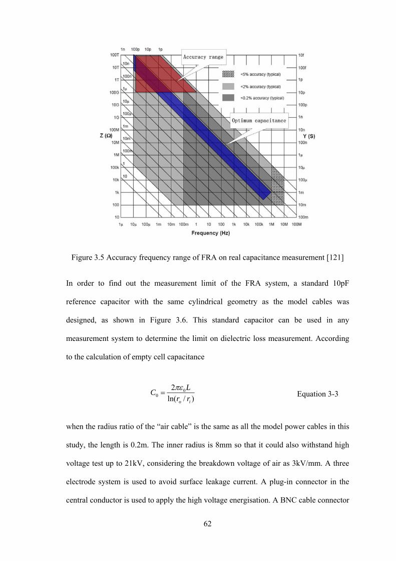
62
Figure 3.5 Accuracy frequency range of FRA on real capacitance measurement [121]
In order to find out the measurement limit of the FRA system, a standard 10pF
reference capacitor with the same cylindrical geometry as the model cables was
designed, as shown in Figure 3.6. This standard capacitor can be used in any
measurement system to determine the limit on dielectric loss measurement. According
to the calculation of empty cell capacitance
)/ln(2 0
0io rr
LC πε=
Equation 3-3
when the radius ratio of the “air cable” is the same as all the model power cables in this
study, the length is 0.2m. The inner radius is 8mm so that it could also withstand high
voltage test up to 21kV, considering the breakdown voltage of air as 3kV/mm. A three
electrode system is used to avoid surface leakage current. A plug-in connector in the
central conductor is used to apply the high voltage energisation. A BNC cable connector

63
on the metal tube is used as measurement electrode while the small measured signal can
be protected by the coaxial cable shield. This “air cable” is made of copper for central
conductor, measuring electrode and guard electrode. PTFE is used to separate guard
electrode and as skeleton to keep the correct distance between two electrodes.
Figure 3.6 Reference capacitor design and photos
With the help of the “air cable”, the FRA system limit can be determined. Because the
air is practically considered loss free and independent of frequency, the loss tangent
measurement result on the “air cable” is the noise floor of the experimental system.
Figure 3.7 shows the measurement results made by the FRA on a homo-polymer model
cable sample at different temperatures and on the “air cable”. In the frequency range
from 10-4Hz to 106Hz, the loss tangent of this homo-polymer model cable sample was
found noisy and increasing at higher frequencies above 1Hz (Figure 3.7). At higher
frequencies, firstly, there is no change of the loss tangent at different temperatures.
Secondly, the loss tangent is in fact the same as that of the “air cable”. Therefore, the
effective accuracy frequency range for FRA technique can be determined as below 1Hz,
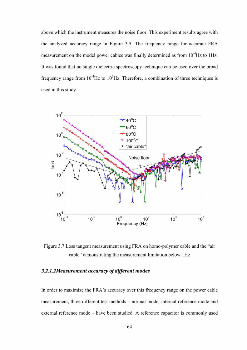
64
above which the instrument measures the noise floor. This experiment results agree with
the analyzed accuracy range in Figure 3.5. The frequency range for accurate FRA
measurement on the model power cables was finally determined as from 10-4Hz to 1Hz.
It was found that no single dielectric spectroscopy technique can be used over the broad
frequency range from 10-4Hz to 106Hz. Therefore, a combination of three techniques is
used in this study.
10-4
10-2
100
102
104
10610
-8
10-6
10-4
10-2
100
102
Frequency (Hz)
tan δ
40oC
60oC
80oC
100oC"air cable"
Noise floor
Figure 3.7 Loss tangent measurement using FRA on homo-polymer cable and the “air
cable” demonstrating the measurement limitation below 1Hz
3.2.1.2 Measurement accuracy of different modes
In order to maximize the FRA’s accuracy over this frequency range on the power cable
measurement, three different test methods – normal mode, internal reference mode and
external reference mode – have been studied. A reference capacitor is commonly used
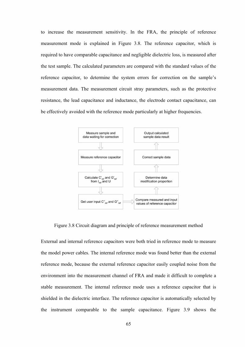
65
to increase the measurement sensitivity. In the FRA, the principle of reference
measurement mode is explained in Figure 3.8. The reference capacitor, which is
required to have comparable capacitance and negligible dielectric loss, is measured after
the test sample. The calculated parameters are compared with the standard values of the
reference capacitor, to determine the system errors for correction on the sample’s
measurement data. The measurement circuit stray parameters, such as the protective
resistance, the lead capacitance and inductance, the electrode contact capacitance, can
be effectively avoided with the reference mode particularly at higher frequencies.
Figure 3.8 Circuit diagram and principle of reference measurement method
External and internal reference capacitors were both tried in reference mode to measure
the model power cables. The internal reference mode was found better than the external
reference mode, because the external reference capacitor easily coupled noise from the
environment into the measurement channel of FRA and made it difficult to complete a
stable measurement. The internal reference mode uses a reference capacitor that is
shielded in the dielectric interface. The reference capacitor is automatically selected by
the instrument comparable to the sample capacitance. Figure 3.9 shows the

66
measurement results on a homo-polymer cable sample with normal and internal
reference mode in the frequency range from 10-3Hz to 10Hz. The real permittivity ε' can
be well measured in both modes and does not have a big difference. However, the
imaginary permittivity ε'' in internal reference mode has negative values at lower
frequencies and false results might be incorrectly displayed with absolute values in FRA
software (SMaRT Version 2.8.0). The negative values are due to the low loss
characteristic of the test cable sample and are produced by the calculation in reference
mode. Although the reference capacitors are very low loss standard components with
stable response in the frequency range, the model power cables have lower loss than the
reference capacitor.
Therefore, the frequency response analyzer technique can be used to measure the low
frequency dielectric response of the model power cables in the range from 10-4Hz to
1Hz. The dielectric loss due to DC conductivity has a slope of -1 in imaginary part as
explained in chapter 2 and makes the measurement easier. At the other frequencies, up
to 1MHz, the dielectric loss is smaller than that due to noise background. This
frequency range is not a fixed region for accurate measurement and depends on the
insulation materials and measuring conditions such as temperature. For example, the
homo-polymer XLPE model cable AAA has no detectable loss until 80°C. Normal
mode was found to be the best method with direct measurement of the cable sample,
because the standard reference capacitors are too lossy to help improve the sensitivity.
The direct measurement will give the most reliable results, despite the small ripple due
to FRA’s instrumental rearranging of the amplifiers.

67
10-3
10-2
10-1
100
1012.2
2.21
2.22
2.23
2.24
2.25
2.26
2.27
2.28
2.29
Frequency (Hz)
ε'
normal modeinternal reference mode
10-3
10-2
10-1
100
101-0.015
-0.01
-0.005
0
0.005
0.01
0.015
Frequency (Hz)
ε''
normal modeinternal reference modefalse result of internal reference mode
Figure 3.9 FRA test of normal and internal reference modes on the complex permittivity
3.2.1.3 High voltage dielectric spectroscopy
The possibility of integrating high voltage amplifier with the FRA system has been
investigated. The circuit diagram of the HV system is shown in Figure 3.10 (a). The low

68
output voltage is amplified through the HV amplifier. The monitoring voltage of FRA is
obtained via an internal potential divider in the HV amplifier. There is a 60pF internal
capacitance that could influence the maximum output frequency in the equation
peakload fUpFCi π2)60( +=
Equation 3-4
(a) HV FRA system diagram (b) HV FRA system with HV divider
Figure 3.10 Circuit diagram for analysis of HV FRA measurement
For high voltage experiment with sensitive small current detector in FRA, a protective
resistor has to be installed in series with the test sample. In the worst case of breakdown,
the protective resistor should be big enough to restrict the current within 20mA, which
is the maximum input current of the FRA, under the maximum voltage of the high
voltage amplifier (20kV Trek 20/20B).
Ω=== MmAkV 1
2020
FRA ofcurrent input maximumamplifier HV of tageoutput vol maximumresistor protective minimum
The cable sample is represented with its parallel equivalent circuit for the convenience
of mathematic modelling. This equivalent circuit will be used all through the study.
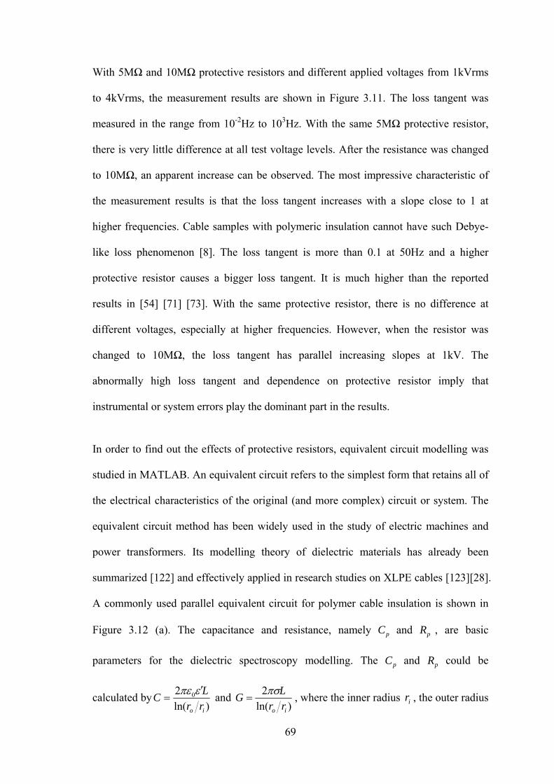
69
With 5MΩ and 10MΩ protective resistors and different applied voltages from 1kVrms
to 4kVrms, the measurement results are shown in Figure 3.11. The loss tangent was
measured in the range from 10-2Hz to 103Hz. With the same 5MΩ protective resistor,
there is very little difference at all test voltage levels. After the resistance was changed
to 10MΩ, an apparent increase can be observed. The most impressive characteristic of
the measurement results is that the loss tangent increases with a slope close to 1 at
higher frequencies. Cable samples with polymeric insulation cannot have such Debye-
like loss phenomenon [8]. The loss tangent is more than 0.1 at 50Hz and a higher
protective resistor causes a bigger loss tangent. It is much higher than the reported
results in [54] [71] [73]. With the same protective resistor, there is no difference at
different voltages, especially at higher frequencies. However, when the resistor was
changed to 10MΩ, the loss tangent has parallel increasing slopes at 1kV. The
abnormally high loss tangent and dependence on protective resistor imply that
instrumental or system errors play the dominant part in the results.
In order to find out the effects of protective resistors, equivalent circuit modelling was
studied in MATLAB. An equivalent circuit refers to the simplest form that retains all of
the electrical characteristics of the original (and more complex) circuit or system. The
equivalent circuit method has been widely used in the study of electric machines and
power transformers. Its modelling theory of dielectric materials has already been
summarized [122] and effectively applied in research studies on XLPE cables [123] [28].
A commonly used parallel equivalent circuit for polymer cable insulation is shown in
Figure 3.12 (a). The capacitance and resistance, namely pC and pR , are basic
parameters for the dielectric spectroscopy modelling. The pC and pR could be
calculated by)ln(
2 0
io rrLC επε ′
= and )ln(
2io rr
LG πσ= , where the inner radius ir , the outer radius

70
or , the length of cable L and the conductivity σ should be known. In this modelling
study, the sample’s length ( cmd 13= ), static dielectric constant ( 3.2=rε ) and
resistance ( Ω= 1510pR ) are used.
10-2
10-1
100
101
102
10310
-3
10-2
10-1
100
101
Frequency (Hz)
tan δ
5MΩ protection, 1kV5MΩ protection, 2kV5MΩ protection, 3kV5MΩ protection, 4kV10MΩ protection, 1kV
ω1
Figure 3.11 High voltage FRA measurement on XLPE model cable with different
protective resistors
Figure 3.12 shows the comparison of loss tangent with different equivalent circuits.
Without protection resistor, the blue curve shows the ideal dielectric response of the
cable insulation. The loss tangent can be calculated as
)()(1tan
ωεωε
ωδ
′′′
==ppRC
Equation 3-5

71
(a) 10-5
100
105
10-10
10-8
10-6
10-4
10-2
100
102
Cable Sample Tan Delta
Frequency
Tan
Del
ta
(b)
10-5
100
105
10-4
10-3
10-2
10-1
100
101
102
Cable Sample Tan Delta with protective resistor
Frequency
Tan
Del
ta
Figure 3.12 Equivalent circuit modelling on the effect of protective resistor
From the equation, it can be seen that the loss tangent is proportional to the reciprocal of
frequency. After installing a 10MΩ protection resistor, the equivalent circuit and
modelling result is shown in Figure 3.12 (b). It can be seen that the loss tangent
increases at higher frequencies. The increasing loss is due to the protective resistor in
series with the cable insulation based on the formula

72
)()()1(
tan 2
2220
ωεωε
ωω
δ′′′
=++
=pp
ppp
RCRCRR
Equation 3-6
At lower frequencies when 1<<ppCRω , the dielectric loss is mainly due to the bulk
conduction of the insulation, 1tan −∝≈ fRC ppωδ . At higher frequencies, when
1>>ppCRω , the sample capacitance tends to short its parallel resistance. In this
situation, fRCp ∝≈ 0tan ωδ . The characteristic frequency can be calculated as
pCRf
021
π= .
102
103
104
OK
warm
hot
very hot
unmeasurable
Frequency (Hz)
8kVrms10kVrms12kVrms
Figure 3.13 Resistive heating of the protective resistor at different voltages
The increasing loss tangent has also been experimentally proved to be due to the
protective resistor, as shown in Figure 3.13. With 5MΩ protective resistor, high voltage
spectroscopy using the FRA and Trek amplifier 20/20B was measured. The frequency

73
started at 100Hz and ended at 10kHz. Three different test voltages were used from
8kVrms to 12kVrms. Five 1MΩ 0.6W carbon film resistors were used as protection.
Temperature level was sensed by hand and recorded right after 1 minute measurement.
It can be seen that at 8kVrms, the temperature of the protective resistors was normal at
100Hz but became hotter when the frequency increased. At 10kHz, it was not possible
to measure current, since it exceeded 10mA, the set maximum set, in the amplifier for
the safety of the FRA. This indicates that more power was consumed in the protective
resistors at higher frequencies because more voltage was applied across them. At higher
voltages, the same situation happened, and more resistive heating occurred at lower
frequencies.
Since the protective resistor should not be removed for the safety of FRA, another
possibility, as shown in Figure 3.10 (b), is to use a HV divider after the protection with
the same ratio arms – 2000:1 – as the HV amplifier, and provide monitoring voltage
from it. This method would exclude all the influence before the voltage is applied to the
test sample. In this case, the potential divider sends a feedback voltage to the FRA that
should be an exact proportion of the instantaneous sample voltage. However, a new
problem would emerge by the HV divider. Every HV divider is originally designed with
electrical component such as resistors and capacitors, it can be perfect only at fixed
frequency and normally has very limited bandwidth. There may be small phase shift in
its working frequency range and the phase change can be comparable or even bigger
than that due to the actual dielectric loss of the cable samples. For example, a tanδ of
10-4 equals a phase angle of 5.73×10⁻³, which is a typical loss tangent angle of XLPE
cables. Artefacts caused by the series resistor or the potential divider can be so much
larger than the cable loss and it is not possible to account for their effects by numerical
correction. Therefore, direct measurement, i.e. without any series resistor and potential

74
divider, provides the most reliable data. HV FRA system can be made with HV divider
to shield the influence of protective resistor, but extra influence would be induced by
the divider itself. Since very low dielectric loss model cables are the measurement
objects in this study, the HV system is not appropriate. Only low voltage experiments
with direct measurements have been carried out.
3.2.1.4 The measurement system setup and specifications
The FRA experiment system in this study is shown in Figure 3.14. The FRA generates a
sinusoidal voltage of desired frequencies into the dielectric interface with “Gen”
channel. Channel V1 sends back the original voltage directly to FRA as “norm” voltage.
“Hi” outputs the voltage to the cable sample through a BNC connection. The current
through the cable sample is measured by “V2” at “Lo”. The voltage of V1 and current at
V2 are used to calculate the complex impedance ∗Z and, therefore, the complex
capacitance ∗C . The FRA, Dielectric Interface and the oven are all controlled by a
computer program (Solartron SMaRT 2.8.0) though GPIB and Modbus connections.
The specifications of the FRA system are:
• frequency range: from 10-4Hz to 1Hz (above 1Hz the dielectric loss below the
noise floor of the FRA technique)
• applied voltage: from 0 to 3Vrms
• current measurement: from 1fA to 100mA
• Tan Delta Range: from 10-3 to 103 in “normal” mode

75
• Capacitance Range: from 1pF to 0.1F (the optimum capacitance should be in the
range from 100pF to 1nF)
• temperature range: from 20°C to 120°C (from 293 to 393K) (limited by the
cable materials below any phase change or glass transition)
In conclusion, the Solartron FRA system was used for measuring at low voltages and at
frequencies below 1Hz.
Figure 3.14 FRA experiment system on power cable measurement
3.2.2 Transformer ratio bridge in the range from 300Hz to 10kHz
In order to measure higher frequency dielectric loss of the model power cables, other
techniques are needed. Having the advantages over the Schering bridge that have been
introduced in chapter 2, the transformer ratio bridge was selected as the dielectric
spectroscopy technique. A universal inductive bridge can be integrated with an external

76
function generator to extend the originally designed frequency range. The transformer
coils become inefficient when below 100 Hz. Above 10 kHz, the balance detector
cannot reach a null. Hence, the frequency range is from 100Hz to 10kHz. However, it
has been found that noise greatly influenced the accuracy and efforts have been made to
extend the frequency range while maintaining accurate measurement for the low loss
model cables.
3.2.2.1 Improvement on measurement accuracy
Because the XLPE cables have extremely low dielectric loss and the measurement
could be easily influenced by background noise and interference such as harmonics,
these issues are the most important and the most difficult thing for precise measurement
on the cable samples. A tuned amplifier has been designed to filter any signal of
frequencies other than the frequency under measurement and finally enlarge the
bandwidth [124]. The circuit of the tuned amplifier is shown in Figure 3.15 (a). A
multiple-feedback analogue filter with resistors and capacitors works to amplify a
specific frequency signal. The desired signal at that specific frequency can be amplified.
Any signal other than the desired frequency is attenuated. In the circuit diagram, VR is a
logarithmic variable resistor used to modulate the “peak” frequency, based on Equation
3-7 [125]
21210
)(21
CCRRRf
Vπ=
Equation 3-7
where the 0f is the frequency to be amplified. In this study, Ω== 3321 RR and
FCC μ121 == , VR was determined as 50kΩ covering the frequency range from 175Hz

77
to 39kHz. In order to prevent excessive current flowing into the circuit, a unity gain
amplifier was placed before the filter.
C1
1u
C2
1u
Rv
50k
R1
33
R233
0
U2
OPAMP
+
-
OUTU3
OPAMP
+
-
OUT
V11Vac0Vdc
VDB
(a) circuit diagram for simulation in PSpice
(b) photo of real circuit in a shielded box
Figure 3.15 Design of tuned amplifier for transformer ratio bridge system
The circuit was simulated on a computer with OrCAD PSpice. A frequency domain
simulation with 1V AC voltage source was done in the frequency range from 100Hz to
10kHz. The output voltage in dB was obtained as shown in Figure 3.16, where the
attenuation in dB is against frequency range from 100Hz to 10kHz. From the results, the
specific signal of the applied frequency is amplified and the other frequencies are

78
attenuated greatly so that the high frequency environmental noise will be much smaller
and will not influence the balance detector of the transformer ratio bridge. The real
circuit of tuned amplifier has been built in a shielded box (Figure 3.15(b)). Two 9V
batteries are used to drive the op-amps and a screwed logarithmic potentiometer is fixed
near the wall of the shielding box so that it could be tapped outside when the shielding
box is sealed.
Frequency
100Hz 300Hz 1.0KHz 3.0KHz 10KHzDB(V(U2:OUT))
-10
0
10
20
30
40
50
Figure 3.16 PSpice simulation result of the tuned amplifier
The system has been further improved against noise from mains power supply. The
bridge circuits were originally designed to be driven by transforming and converting the
mains supply. It was found with the samples and the tuned amplifier circuit being
shielded, extremely small interference from the harmonics of the mains power can also
make it difficult for the bridge to reach perfect balance. Therefore, a DC battery was
used to replace the mains power supply. The battery is directly connected to the circuit
of balance detector and is driving it without bringing any harmonics. It was found even
higher precision was obtained by this means.

79
3.2.2.2 Experimental system setup
The transformer ratio bridge experiment system for low loss power cable measurement
is shown in Figure 3.17. The system has been integrated with Wayne Kerr universal
bridge B221 [126], function generator, tuned amplifier specially designed for improving
system sensitivity, oscilloscope and temperature control oven to accommodate cable
samples.
Figure 3.17 Transformer ratio bridge measurement system setup
The function generator is used as an external voltage source for the inductive bridge.
The sinusoidal voltage is applied from the secondary windings of the bridge on the
cable sample in the oven. According to the principles introduced in chapter 2, anti-phase
voltage is therefore applied on the standard variable impedance inside the bridge. By
adjusting the capacitance and conductance taps, the currents from the two halves of the
bridge will be neutralized only when the impedance is the same as that of the cable

80
sample, which is hung in the oven for temperature control. The balance detector on the
bridge shows null when the bridge is balanced. For higher resolution, the balance can be
more sensitively monitored by the oscilloscope, which is connected to externally
monitor the bridge. With the help of a tuned amplifier, the balance can be detected
below 1kHz and the system frequency range has been extended down to 300Hz. Before
measurement, the system can be calibrated with null buttons to cancel out the lead effect
and background noises. For the transformer bridge system, the output voltage is limited
below 2Vrms. A higher output voltage may cause the output voltage waveform to be
distorted, because a higher current would be required for the secondary windings and
this could saturate the winding coils.
The specifications of the transformer ratio bridge system are:
• frequency range: from 300Hz to 10kHz
• applied voltage: from 0 to 2Vrms
• capacitance range: from 1 to 999pF
• conductance Range: from 10-9S to 10-6S
• tanδ range: >10-5
• temperature range: from 20°C to 120°C (from 293K to 393K)

81
3.2.3 Time domain charging/discharging current technique in the range from
1Hz to 250Hz
Because of the sensitivity limit of frequency domain techniques, time domain dielectric
spectroscopy was used in this study to fill the gap between the other two frequency
domain techniques in this study, as shown in Figure 3.18.
Figure 3.18 Combination of three dielectric spectroscopy techniques
The charging/discharging or polarization/depolarization current measuremental system
has been designed and developed to meet the requirement of very low loss power cable
measurement. As introduced in chapter 2, the charging/discharging system measures
charging and/or discharging currents versus time. The time domain data can be
transformed into frequency domain to obtain frequency spectra of permittivity and loss
tangent. For low loss measurement of power cables, the current sensitivity and anti-
noise methods are important for accurate measurement. In this research study, the
experiment system was developed with two different designs. Based on the problems
that were found in the original designed system, a novel system has been finally

82
developed with the ability to measure the loss tangent of the model power cables in the
frequency range from 1Hz to 250Hz.
3.2.3.1 The original experiment system design
The original charging/discharging experiment system was designed with a
commercially available HVDC supply (Glassman Ltd), self made high voltage switch,
Keithley picoammeter model 6485 and protection circuit, as shown in Figure 3.19.
When measuring the cable sample in the test unit, the switch-on of the power supply
starts the charging current measurement and the high voltage switch controls the
commencing of discharging current measurement. The current is measured by the
picoammeter that is connected to the computer and driven by LabVIEW program. The
switch-off action for starting discharging measurement can tell the computer program
via parallel port so that the data storage can be synchronized with the switch action.
Figure 3.19 Basic design of charging/discharging experiment system
The test unit is originally designed as shown in Figure 3.20(a). It is made of an
aluminium box with a copper chassis to reduce electromagnetic noise while the copper
83
chassis could maintain a good contact to ground. A three electrode system is used here.
Conductor balls at both two ends of the cable sample have a diameter of 30mm which is
enough to prevent corona. The gap from the balls to the metal walls is at least 50mm
which could stop the danger of breakdown up to 50kV, according to the engineering
consideration of 1kV/mm breakdown strength in the air. Metal brackets are used for
holding the cable samples and provide a channel through which the guard electrode
could be connected to the copper chassis. A high voltage switch is incorporated inside
the test unit and will be discussed later. Another small aluminium shielding box is
placed inside the test unit box to accommodate a protection circuit. The picoammeter
incorporates protection circuitry against nominal overload conditions. However, a
voltage higher than the maximum voltage (220V Peak) value for the selected current
range, and the resultant current surge could damage the input circuitry [127]. Adding a
resistor and two diodes (1N3595) provides considerable protection. The resistor must be
large enough to limit the current through the diodes to 20mA or less, and be large
enough to withstand the supply voltage. A 5MΩ carbon film resistor is enough to limit
the current to 10mA when the voltage is 50kV. The two diodes prevent voltages of
more than about 0.6V appearing across the input of the picoammeter even when the
voltage polarity changes. They are put inside the light-tight conductive shield because
their light sensitive property would cause noise when exposed to varying light intensity.
A photo of the test unit is shown in Figure 3.20(b).
The high voltage switch plays an important role to switch charging current
measurement to discharging current measurement. A high voltage switch was designed
as shown in Figure 3.21. The main part (Figure 3.21(a)) is made of nylon and its
dimensions are designed so that it will just fit into the test unit with good insulation. A
switch bar (Figure 3.21(b)) with metal body and nylon handle is used to change the

84
measurement from charging to discharging. Through the metal balls and domes high
voltage can be applied to the cable sample for charging current measurement. When
discharging measurement should start, the switch bar is pressed to the end of the nylon
box as quickly as possible in order to save as much high frequency information as
possible.
(a) the high voltage cable sample test unit design
(b) photo of the test unit containing high voltage switch and a cable sample
Figure 3.20 High voltage test unit for the charging/discharging experiment system

85
(a) 3-view chart of the main part

86
(b) fittings of metal contacts
Figure 3.21 The high voltage switch design for charging/discharging experiment
There are two spring loaded contacts in the switch, one of which is connected to the
copper chassis as ground connection. The other one is connected to the computer’s
parallel port through a communication circuit, as shown in Figure 3.22. When the
charging current is measured, the spring loaded contact will float and 5V DC power will
drag the port to logical “1” through a 1kΩ resistor. Pin 1 of parallel port (Strobe)
provides logical “1” to pin 10 (Ack), which tells LabVIEW program that charging
current is being measured. When the high voltage switch is pressed, the discharging
current measurement starts. At this starting point, the spring loaded contact will be
grounded and make pin 10 logical “0”. This design can tell the computer software to

87
change accordingly when discharging begins. A 5.1V breakdown diode is also in the
circuit to protect the input port in case there is too much residual charge from the high
voltage switch.
Figure 3.22 Parallel port control for discharging current measurement
LabVIEW 8.0 (Laboratory Virtual Instrumentation Engineering Workbench) was
originally chosen as a program platform for the charging/discharging system. LabVIEW
is a platform and development environment for a visual programming language from
National Instruments. It is commonly used for data acquisition, instrument control, and
industrial automation on a variety of platforms including Microsoft Windows, various
flavors of UNIX, Linux, and Mac OS [128] [129]. In order to measure precisely the
extremely small current, a Keithley picoammeter 6485 is used. A picoammeter is an
ammeter built along the lines of the ammeter function of an electrometer [130].
LabVIEW also has a support for the Keithley picoammeter 6485 so the instrument
driver could be programmed using the function toolbox.
The program was designed to have the function of measuring charging and discharging
currents separately. The main software flowchart is shown in Figure 3.23. Before
running the program, it is important to leave the picoammeter or electrometer power on

88
for at least 1 hour. This warming up period makes sure the instrument has the most
accurate performance, especially for low level measurements. Background noise from
the earth or Johnson noise from electric components should also be measured, stored
and subtracted in the end. In the main program, some basic parameters, which include
acquisition interval and measurement points, can be defined before measurement starts
and some other initialization for the program interface will also finish firstly. Following
the initialization, background noise data is loaded for correction of measurement data.
Then the program will wait for the start button to be pressed when the high voltage is
applied, after which the charging current is measured until the input port changes to
logical “0” which means the high voltage switch is pressed to the discharging position.
Then, discharging current will be measured according to the set points in the program.
Charging and discharging currents are shown in real time in the program with both
linear and logarithmic scales. All measurement data is saved for further analysis.
Figure 3.23 LabVIEW program flowchart for charging/discharging experiment system

89
3.2.3.2 Problems with the original experimental system
A photo of the original charging/discharging system is shown in Figure 3.24. A
Glassman high voltage DC power supply is used to supply up to 15kV on the 13cm
cable sample inside the test unit in a fridge which is used as a temperature controller.
High voltage cable glands are used to prevent leakage current and breakdown. Charging
and discharging currents can be measured through a BNC coaxial cable that connects
the protection circuit of the test unit to the input of the picoammeter. A GPIB card is
used for instrument control and data acquisition by the LabVIEW program. When the
high voltage DC power supply is switch on, the program should be clicked to run at the
same time. When the high voltage switch in the temperature-controlled cabinet is
pressed, the sample starts discharging and the status change is automatically detected by
the program via a computer parallel port.
Figure 3.24 Charging/discharging experiment system with picoammeter

90
100
101
102
103
10410
-13
10-12
10-11
10-10
10-9
10-8
10-7
10-6
Time (s)
Cur
rent
(A
)
20C30C40C50C
Figure 3.25 Charging current measurement on cable AAA
Typical charging current measurement results on a homo-polymer cable (AAA) is
shown in Figure 3.25. The measurement was taken from 1s to 3×10⁴s (9 hours) at
different temperatures. The current decayed from about 10-7A to 10-12A in the first 100s.
Afterwards, the current was in the noise floor and it cannot be correctly measured. The
problem is caused by two reasons:
• The cable sample is too short to allow detectable current flowing through the
insulation. According to )ln(
2io rr
LG πσ= , the conductance of the cable sample is
proportional to the sample length, provided the conductivity is constant.
Therefore, increasing the cable sample length can increase the current at the
same applied voltage. When the current is much bigger than the noise floor, the
charging and discharging process can be precisely measured. Based on tests for

91
all dielectric spectroscopy techniques, the minimum cable sample length has
been determined as 5m.
• The noise from the power supply is another important issue for
charging/discharging current measurement. The noisy measurement results,
shown in Figure 3.25, was found to be at the level of ±5pA, which is difficult to
tell the actual conduction of cable sample even using long time averaging
method. The reason is that the commercial supply converts mains frequency
voltage with power electronics converter and there are small high frequency
fluctuations at the output. This voltage fluctuation is not negligible for the low
current measurement on XLPE cables, according to equation
dtdVC
RVi +=
Equation 3-8
where i is the total measured current, V is the applied DC voltage, R is the
cable insulation resistance and C is the cable capacitance. Because the DC
conduction part is very small around pA, the small voltage fluctuation will cause
big influence in the total detectable current through the sample. More details can
be found in [131].
The charging/discharging current in the first second is important in this study because
the frequency range gap between the frequency response analyzer and the transformer
ratio bridge can be covered within this time duration. In order to measure the dielectric
response over the range from 1Hz to 200Hz, for example, the sampling rate should be at
least 400 sample/second. From the measurement results in Figure 3.25, the sampling
rate is 1 sample/second. It is difficult to increase the sampling rate further because the

92
instrument has a response time of about 16ms and there is no precise synchronization at
the starting point. The problem was found to originate mainly from the electrometer but
also due to the limited speed of the LabVIEW program. The internal circuit structure of
a typical electrometer, including Keithley picoammeter 6485, is shown in Figure 3.26.
The input signal is magnified by preamp according to a different function/range. The
output of the preamp amplifies the original signal. The pre-amplified signal is sampled
by a micro-processor, which determines the further ranging amplifier for final output.
The final output is the signal after multiple amplifications, and this process needs
hundreds of milliseconds typically. The sampling rate is greatly reduced using such
commercial picoammeter or electrometer. Besides, LabVIEW program with GPIB has
still about 20ms software delay at the beginning of the measurement. This will result in
incorrect measurement data because the charging/discharging current is actually
recorded 20ms after the voltage application.
Figure 3.26 Internal circuit diagram of electrometers [130]

93
The principle of the charging/discharging current measurement requires that a step
voltage be applied to the sample. In practice, there is always a rising/falling time for the
voltage application. In order not to bring negative effect into the measurement results,
the rise/fall time should be small enough for specific requirements. The commercial
high voltage DC power supply in the original design was tested with a falling time of
about 800ms, as shown in Figure 3.27. This substantially influences the discharging
current measurement because the applied voltage cannot drop down to zero when the
discharging current measurement has already started.
Figure 3.27 Switching time of commercial high voltage DC power supply
3.2.3.3 Development of novel charging/discharging experiment system
Based on the knowledge gained from the original charging/discharging experimental
system, a novel measurement system has been developed, as shown in Figure 3.28. The
new system incorporates a 1kV battery supply, high voltage toggle switches, a potential

94
divider as voltage monitor, a current-voltage converter and a storage oscilloscope. The
commercial high voltage DC power supply was replaced by a hand-made battery supply
with a very low ripple output voltage so that the conduction current of cable insulation
can be accurately measured. High voltage toggle switches are used to make faster
switching actions. As required from the other two measurement techniques, the switch
should ideally have falling (switch-off) time less than 1ms, in order to include a
frequency response up to 500Hz by Nyquist law. A resistive potential divider can be
used to monitor the response. The charging/discharging current is converted by a fast
converting electrometer. The voltage tolerance of the current-voltage converter is also
considered because the transient current may exceed the maximum input voltage and
damage the circuit. The oscilloscope is a digitizer of data with different channels
working at the same input signal to overcome the digitizing problem. In this study, a
four channel storage oscilloscope is used. One channel is connected to the potential
divider as a voltage monitor and measurement trigger; the other three channels are in
different resolutions from 1mV/div to 2V/div. By using several channels on the
oscilloscope at different gains, the problems associated with changing ranges on the
electrometer are obviated. This allows the current to be measured as it decays quickly
over several decades without the necessity to change ranges on the oscilloscope. The
data from different channels can be merged together.
The structural design of the DC battery supply, consisting of a high voltage toggle
switches and resistive potential divider, is shown in Figure 3.29. One hundred and
twenty 9V batteries are connected in series to get approximate 1kV voltage. The
double-pole toggle switch can provide both positive and negative polarities. Another
single-pole switch is used to earth the sample for discharging current measurement. A

95
high voltage capacitor is used together with the resistance potential divider to help hold
the high voltage during the switching transient.
Figure 3.28 Discharging current measurement system setup
Figure 3.29 High voltage battery supply design diagram
Photographs of the actual high voltage battery supply are shown in Figure 3.30. The left
photo shows the inside view; 30 batteries of the top layer are inter-connected in series
while the other three layers are below the top one. A shielding box is used to prevent

96
environmental noise and provide a solid container for the batteries. Plastic foams and
wooden plates are used to separate different layers and prevent any contact with the
shielding box. The final output is wired into a plastic box on top of the aluminium
shielding box, as shown in the right photo with a top view. A high voltage BNC
connector is used to output the high voltage and another common BNC connector is the
monitor output. Polarity switch and charging/discharging switch can be controlled from
the top of the plastic box.
Figure 3.30 Photos of high voltage battery supply
The response time of the supply was checked by an oscilloscope through the monitor
connector. The response time can be found in Figure 3.31 and a comparison between
the battery supply (blue curve) and the former commercial one (red curve) can be made
(note that the two curves have different time scales). From the results, the battery supply
has a falling time of about 500µs, while the commercial one has a falling time of about
1s. Therefore, the new battery supply can provide more than 1000 times faster response
time and guarantee the switch action will not have influence on discharging current
measurement.

97
Figure 3.31 Comparison of response time between commercial supply (red) and the
battery supply (blue)
Because the new supply is made of DC batteries, there are no high frequency harmonics
or ripple on the output voltage. The only source of voltage fluctuation might be from the
environment temperature, which influences the chemical reaction rate inside the
alkaline battery. In order to make sure this will not cause a problem to the conduction
current measurement, two batteries in series are measured under different temperatures
from 10°C to 50°C. The result is shown in Figure 3.32, indicating a 0.3V/50°C variation
that is equal to 18V/50°C or 0.36V/°C for 120 batteries. With a 5m cable sample in our
study, the cable’s capacitance can be calculated as about 800pF. Assuming 1pA current
would be damageable to the results measured from this sample, according to equation
dtdVCi =
Equation 3-9
the maximum voltage variation is
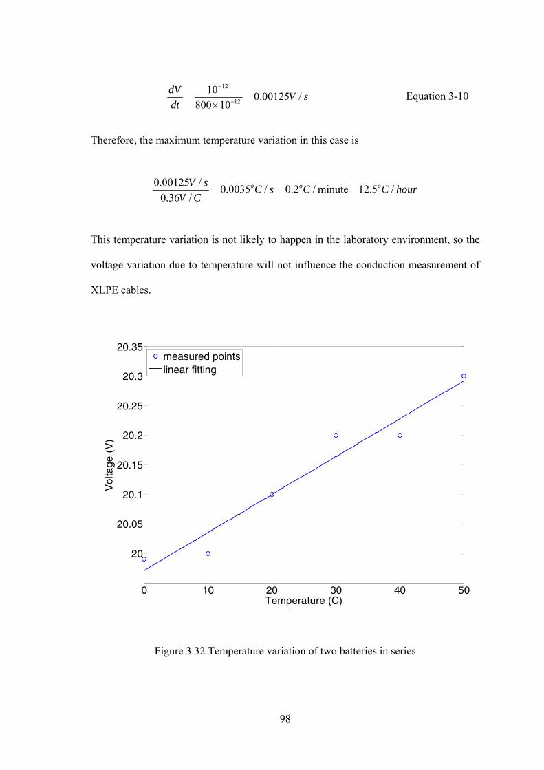
98
sVdtdV /00125.0
1080010
12
12
=×
= −
−
Equation 3-10
Therefore, the maximum temperature variation in this case is
hourCCsCCV
sV ooo /5.12minute/2.0/0035.0/36.0
/00125.0===
This temperature variation is not likely to happen in the laboratory environment, so the
voltage variation due to temperature will not influence the conduction measurement of
XLPE cables.
0 10 20 30 40 50
20
20.05
20.1
20.15
20.2
20.25
20.3
20.35
Temperature (C)
Vol
tage
(V
)
measured pointslinear fitting
Figure 3.32 Temperature variation of two batteries in series

99
The commercial electrometer was replaced in this design by a bespoke current to
voltage converter. The current to voltage converter is required to have reliable
amplification in the frequency range for discharging current measurements. The current
to voltage converter has different ranges. Ideally, the higher amplification range should
be used, but the -3dB bandwidth becomes smaller as the gain is increased. The ranges
with 10-8A/V (range 2) and 10-7A/V (range 3) have been tested. A function generator
was used to generate signals of different frequencies from 10Hz to 1000Hz. Bode plots
of the measurement results have shown that the -3dB frequency of Range 2 is at 30Hz
above which the attenuation cannot be accepted for the measurement. Range 3 has
improved -3dB amplitude attenuation frequency at about 280Hz (Figure 3.33) and has
been chosen to convert the current in this measurement. Range 2 can still be used to
increase the current sensitivity, but only the current at longer time than 1s is not affected
by the bandwidth limitation.
101
102
103-14
-12
-10
-8
-6
-4
-2
0
-3
Frequency (Hz)
Gai
n (d
B)
280Hz
Figure 3.33 Bode plots of current-voltage converter

100
The frequency range from 1Hz to 250Hz requires the measurement to start within the
first 1/500th of a second with a subsequent sampling rate of 500 samples/second and to
finish at 1s. Since the digitizing speed of the oscilloscope can provide up to GHz
sampling rate, measuring the discharging current of the cable samples correctly and
accurately in the first 1 second needs several considerations about the influence of
protective resistor and the current to voltage converter bandwidth. As shown in Figure
3.34, equivalent circuits were built to study the effects of system components on the
measurement accuracy of the model cable samples. Similar to the values of the cable
samples, C1, C2 and R2 simulate their equivalent circuit with a loss peak, which can
vary with different R2 values. C1 and C2 are fixed capacitance of 1nF and 200pF. R2
has up to five different values from 50MΩ to 500MΩ.
Figure 3.34 Equivalent circuit of charging/discharging current measurement system

101
With the protective resistor R1=2MΩ and the current to voltage converter in range 3
(250Hz bandwidth), the discharging current measurement results are shown in Figure
3.35. There are five results for different R2 values. The sampling rate is 10k
sample/second and the measurement duration is 0.5s. Two different processes can be
identified. In the very beginning with 2ms, the current for all cases decayed fast down to
10-6A. Then, the second process started to dominate with different decaying currents,
which are due to different R2 values. Therefore, the second process or long-term
discharging currents represent the relaxation of the test object, while the beginning
decaying currents are just the response of the protective resistor in series with the test
sample. The time constant of the circuit due to protective resistor
msnFMCR 21211 =×Ω=×=τ
Therefore, in frequency domain, there should be a peak at the frequency that can be
calculated by
12 == τπωτ f
Equation 3-11
The peak frequency
Hzf 6.791022
12
13 =××
== −ππτ
This loss peak at 79.6Hz brought by the protective resistor can be found in Figure 3.36.
The discharging currents in Figure 3.35 were transformed into frequency domain using
Discrete Fourier Transform (DFT), which is introduced in details in section 4.3.2, and
the loss part – imaginary permittivity was obtained. For different R2 values, the loss
peaks were calculated by Equation 3-11. There is generally coherence between the

102
transformed result of the measurement data and the calculated result of the loss peak
frequencies, although disagreement is found due to the resolution of the measurement
system. However, there is a much bigger loss peak, regardless of R2 value, at about
80Hz. This further proved that the protective resistor can bring big influence to the
discharging current measurement of the model cable samples. Correct results cannot be
measured if this loss peak is not removed from the frequency range from 1Hz to 250Hz.
0 0.1 0.2 0.3 0.4 0.510
-9
10-8
10-7
10-6
10-5
10-4
10-3
time (s)
curr
ent (
A)
50MOhm100MOhm200MOhm400MOhm500MOhm
Figure 3.35 Discharging current of system equivalent circuits
Efforts have been made to remove the influence of the protective resistor while keeping
the current to voltage converter safe from breakdown due to overload current, which is
typically several milli-amps for an operational amplifier. in order to protect the current
to voltage converter and keep it operate with high precision, input current less than
10mA should be guaranteed. Hence, 100kΩ protection was chosen as optimum value.

103
The equivalent circuit measurement result with 100kΩ is shown in Figure 3.37. This
resistance is 20 times smaller than the result in Figure 3.36. After transforming the
discharging current into frequency spectra, the induced loss peak can be shifted to 20
times higher frequency at 1492Hz, which is 6 times higher than 250Hz – the maximum
frequency for this technique. As a result, the response of test sample can be correctly
measured and the influence of the protective resistor has been reduced to minimum. For
all the discharging current measurement in this study, this 100kΩ protective resistor is
jointly used with two back-to-back diodes in a shielding box between the cable sample
and the current to voltage converter input.
100
101
102
10310
-1
100
101
Frequency (Hz)
ε''
50MΩ100MΩ200MΩ400MΩ500MΩ
15.92Hz3.98Hz1.99Hz1.59Hz
7.96Hz79.58Hz
Figure 3.36 Frequency spectra (imaginary permittivity) of the discharging currents
measured on the system equivalent circuits with 2MΩ protection

104
100
101
102
103
10-1
100
frequency (Hz)
ε''
50MΩ200MΩ500MΩ
1492Hz
Figure 3.37 Frequency spectra (imaginary permittivity) of the discharging currents
measured on the system equivalent circuits with 100kΩ protection
3.2.3.4 Experiment system specifications
The novel charging/discharging experiment system was used to measure various types
of model cables in the time duration from 1ms to 10s. Discharging current is measured
to study the depolarization of the cable insulation. Charging current is then measured to
study the conductivity of different cables. By adding the contribution due to DC
conductivity, the dielectric spectra in the frequency range from 1Hz to 250Hz can be
finally obtained. During the measurement, the cable sample is put in an oven under a
fixed temperature for more than three hours to reach thermal equilibrium and then the
battery power supply applies 1kV to the sample for about three minutes, which ensures
that the sample is fully charged for discharging current measurement (recommended
charging time is at least 10 times longer than discharging time [2] [44]). When the high

105
voltage switch is switched to earth, the oscilloscope detects this action by the potential
divider inside the battery supply and then triggers measurement in the other three
channels, with different digitizing resolutions. Data is saved on a floppy disk of the
storage oscilloscope and transferred to computer for analysis.
The specifications of the charging/discharging current measurement system are:
• applied voltage: 1kV DC
• power supply rising/falling time: 50ms/500µs
• discharging current measurement time: 10s
• oscilloscope sampling rate: 500 sample/second
• frequency range: from 1Hz to 250Hz
• tanδ range: >10-6
• temperature range: from 20°C to 120°C (from 293K to 393K)
3.3 Experimental procedures
3.3.1 Degassing and ageing of the model cables
All model cables in Table 3.1 were produced and sent from Borealis in Sweden in
sealed bags to prevent the cables from degassing. These “fresh” cables were cut into 5m
lengths for different experiments.

106
In order to study the degassing effects on the conductivity of different types of the
model cables, fresh cables were degassed in the air and in a vacuum oven. The fresh
model cables with volatile by-products still inside the insulation were firstly measured
with the battery power supply. Then, the cable samples were put in a normal oven under
80°C for five days. After this air degassing procedure, the cable samples were measured
again. Afterwards, the vacuum oven was used for further degassing for another five
days under 80°C. Measurement was taken on the same cable sample for comparison
with previous results.
Figure 3.38 Comparison of aged and non-aged model power cables
In order to study the ageing effects, different types of degassed cable samples were
thermally aged under the temperature of 135°C, which was suggested by Borealis. The
thermal ageing is an accelerated ageing process, and imitates the long term actual
thermal ageing condition of power cables. In Figure 3.38, the effect of ageing on cables
without outer semicon layer can be observed. The colour of the XLPE insulation layer
After ageing
Before ageing

107
changed from grey to dark brown, which indicated chemical reactions happened inside
the insulation material. Similarly, all the other cables with outer semicon have extra
dark brown colour after the thermal ageing process.
3.3.2 Experimental plan on different XLPE model cables
With the three dielectric spectroscopy experiment systems developed, the dielectric
response over a wide frequency range, all temperatures and voltages can be studied.
Different aspects of the model power cables have been studied with five kinds of
experiments.
1. Dielectric spectroscopy measurement of different model cables. As the most
important aim of this research project, the dielectric response of model cables
with different insulation and semicon shields was studied. Measurements on
different model cables with all three dielectric spectroscopy techniques were
carried out to examine the electrical properties and loss mechanisms. This wide
range of frequencies and temperatures will help to understand the origins of
dielectric loss in cable insulation.
2. Degassing effects study. Since degassing can practically enhance the insulation
performance and is the most popularly used method to make the fresh cables
ready for use, degassing effects on different cables were studied by conductivity
measurement, which is an effective way to study the influence of by-products.
3. Ageing effects study. The electrical properties after ageing determine the
reliability of power cables in operation. Based on the apparent difference
between degassed and aged cables, as shown above in Figure 3.38, the

108
conductivity and discharging current were measured on different cables to study
the thermal ageing effects.
4. Semicon material measurement as a complementary study. The dielectric loss
of cables is dependent on the semicon shields, as some studies in recent year
have found [118] [119] [120]. As an essential part of the power cable insulation,
both standard and super-smooth semicon materials were measured as
complementary experiments to study the origin of dielectric loss in the model
power cables.
5. High electric field measurement at power frequency 50Hz. Using Schering
Bridge, the field dependence of the dielectric loss of model power cables were
studied at different voltages.
6. Morphologic study with scanning electron microscopy (SEM). The
microscopic morphology of the model cables was studied using SEM. The test
results can provide some basic information of the model cables and useful
reference for data analysis.
The temperature dependence was studied for all kinds of experiment, because
temperature is a critical parameter for the electrical properties of power cables.
According to the test results in Figure 3.39, at least three hours are needed for the
cable sample to reach thermal equilibrium. Hence, for all experiment, three hours
were left before starting the measurement. In order to compare various cables and
different kinds of experiment, four temperatures have been studied: 20°C, 40°C,
60°C and 80°C. These temperatures can maximally cover the operating temperature
of power cables without melting the cable samples.

109
0 1 2 3 4 5 6 7 8 9 10 11 12 13 14 15 16 17 1820
22
24
26
28
30
32
time (hour)
tem
pera
ture
(o C
)
Figure 3.39 Thermal equilibrium time for model cable experiment. Measurement was
made on a homo-polymer cable sample in an oven from 20°C to 30°C.
Besides the experimental work, computer simulations for analyzing the measurement
data with equivalent circuit method have been used. Based on the measurement results,
the thermal breakdown of the model power cables was also studied.
3.4 Conclusions
The sample preparation method and experimental systems are studied in this chapter:
1. A new sample preparation method for the power cable samples is proposed
using the conductive adhesive copper tapes in order to keep good contact with
the measuring electrode and avoid extra influence due to the outer semicon layer.

110
2. The FRA experimental system has a sensitivity of 10-3 for loss tangent
measurement in the frequency range 10-4Hz to 1Hz. Normal mode should be
used for low loss measurement.
3. A transformer ratio bridge system was developed for measuring the model
cables at higher frequencies from 102Hz to 104Hz. Tuned amplifier was
designed to extend the frequency range. Battery is used to drive the bridge with
higher sensitivity.
4. TDDS system was developed to measure the frequencies from 10-1Hz to 102Hz.
A noise-free high voltage supply was made with batteries. The high voltage
switch, protective resistor and bandwidth of current-voltage converter have been
found to be critical for accurate measurement their parameters were determined
experimentally for the low los measurement on the model power cables.

111
4 Dielectric response analysis of model power cables
This chapter presents the measurement data of various model power cables with the
dielectric spectroscopy experimental systems developed in chapter 3. Section 4.1
analyzes the data measured using the FRA technique. DC conductivity loss in the power
cables dominates the dielectric loss at low frequencies. Section 4.2 analyzes the data
measured with transformer ratio bridge system. The contribution due to semicon layers
has been studied with equivalent circuit modelling in MATLAB. Section 4.3 studies the
discharging current measurement results and the frequency spectra found using Fourier
transforms. Combination of all the data in section 4.4 provides a wide frequency range
dielectric spectra that help understand the mechanisms of dielectric loss in polymer
power cables. In section 4.5, the measurement results on fresh, air degassed and vacuum
degassed cable samples are compared in order to find the degassing effects.
4.1 Dielectric response at low frequencies of from 10‐4Hz to 1Hz
4.1.1 Thermal expansion calibration
The degassed model cables of AAA, ABA, ACA, and BAB have been measured using
the FRA system. Thermal expansion of the model power cables needs be considered
because the cable insulation swells when the temperature increases. Complex
capacitance of the test sample ∗C is calculated from measured complex impedance ∗Z
∗∗ =
ZjC
ω1 Equation 4-1

112
where j is imaginary unit and ω is angular frequency. The complex permittivity ∗ε
can be calculated with the geometric capacitance 0C
0CC∗
∗ =ε Equation 4-2
The thermal expansion coefficient for copper is 1.7×10⁻⁵/˚C and it is much smaller than
the coefficient for polyethylene in Table 4.1. The length of the cable sample does not
change because the inner copper conductor holds the polymer layers from expanding its
length. Therefore, the assumptions have been made that the radius of the inner copper
conductor and the length of the cable sample are constant during thermal expansion, the
outer radius or is the only variable to influence the geometric capacitance 0C in the
equation:
)/ln(2 0
0io rr
LC πε= Equation 4-3
From Equation 4-3, the empty cell capacitance 0C will be smaller when or increases
due to thermal expansion.
Thermal expansion was corrected based on the coefficient table for polyethylene in
Table 4.1. Figure 4.1 shows the real permittivity measurement results (solid lines) on a
homo-polymer cable in comparison with the results after corrections for thermal
expansion (dashed line). An increment of about 0.1 can be seen from 20°C to 80°C.
After thermal calibration, the results have been corrected with smaller gaps between
different temperatures. The gaps that are still present are due to the actual permittivity
change of the material at different temperatures. The decreasing real relative

113
permittivity ε' of polyethylene at higher temperatures was also observed and published
[133], as shown in Figure 4.2. The temperature dependence of the relative permittivity ε'
for 12 µm thick PE film sample was measured at the frequency of 100 Hz (result of
calorimetric measurements is shown for comparison). Tg and Tm are glass transition
temperature and melting point respectively. In the temperature region from 20°C to
80°C, it can be seen that the permittivity of polyethylene decreases at higher
temperatures. In this study, all the measurement results were calibrated before analysis.
Table 4.1 Thermal expansion coefficient for polyethylene [132]
Celsius Linear coefficient. (×10-5/˚C) Volumetric coefficient (×10-5/˚C)
20 23.7 71
25 24.8 74
40 29 87
60 33.7 101
80 40.3 121

114
10-4
10-3
10-2
10-1
1002
2.05
2.1
2.15
2.2
2.25
2.3
2.35
2.4
2.45
2.5
frequency (Hz)
ε'
20C40C60C80C40C, calibrated60C, calibrated80C, calibrated
Figure 4.1 Thermal expansion calibration on ε' of cable AAA
Figure 4.2 Temperature dependence measurements of the real permittivity on
polyethylene [133]

115
4.1.2 Temperature dependent dielectric loss
The FRA measurement results of real and imaginary permittivity on model cables with
different insulation materials and same semicon shields are shown in Figure 4.3, Figure
4.4 and Figure 4.5. In these figures, imaginary permittivity at different temperatures is
shown in solid lines with left y-axis, while real permittivity is shown in dashed lines
with right y-axis. The results for cable AAA are shown in Figure 4.3. It can be seen that
this homo-polymer XLPE cable has the best insulation material with the lowest
dielectric loss. The imaginary permittivity below 80°C is below the noise floor of about
10-3. Only at 80°C, ε'' shows an increasing slope of -1 towards lower frequencies with
the value of 0.14 at 10-4Hz. The real permittivity ε' does not change in this frequency
range under these four temperatures, which indicates that the dielectric loss in ε'' is
likely to be due to DC conductivity loss of the cable insulation. The “ripples” in ε'' are
due to instrumental errors when measuring such low loss samples, as the equipment
switches in different reference components.
Figure 4.4 shows the measurement results on the other homo-polymer model cable
ABA which has different low density polyethylene (LDPE) base resin. The imaginary
permittivity ε'' is bigger than that of cable AAA. At 10-4Hz, ε'' is 2.54×10⁻² at 60°C and
4×10⁻¹ at 80°C. It has parallel slopes of -1 for these two temperatures. Since the real
permittivity stays unchanged, the dielectric loss of this homo-polymer cable is also due
to DC conductivity.
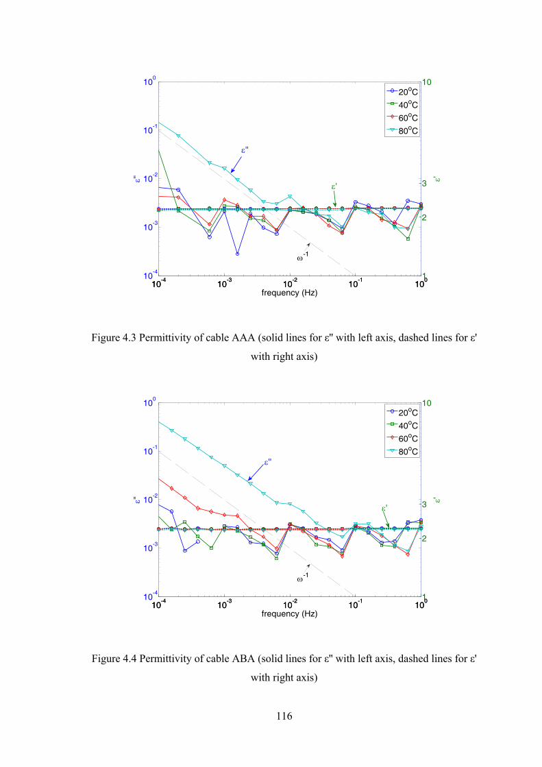
116
10-4
10-3
10-2
10-1
10010
-4
10-3
10-2
10-1
100
frequency (Hz)
ε''
10-4
10-3
10-2
10-1
1001
10
2
3 ε'
20oC
40oC
60oC
80oC
ε''
ε'
ω-1
Figure 4.3 Permittivity of cable AAA (solid lines for ε'' with left axis, dashed lines for ε'
with right axis)
10-4
10-3
10-2
10-1
10010
-4
10-3
10-2
10-1
100
ε''
10-4
10-3
10-2
10-1
1001
10
2
3
frequency (Hz)
ε'
20oC
40oC
60oC
80oCε''
ε'
ω-1
Figure 4.4 Permittivity of cable ABA (solid lines for ε'' with left axis, dashed lines for ε'
with right axis)

117
Unlike the homo-polymer cables, the measurement results of cable ACA (Figure 4.5)
with co-polymer insulation have a different dielectric response. The imaginary
permittivity ε'' is bigger than those of homo-polymer cables and can be identified for all
the temperatures. ε'' has almost parallel lines for different temperatures and similar
intervals between adjacent measurement temperatures. However, ε'' does not have
straight slopes of -1 at higher temperatures of 60°C and 80°C. A loss peak adds to ε'' at
lower frequencies. This can be confirmed by the increment in real permittivity ε' at
these two temperatures. Therefore, the dielectric loss of the co-polymer cable has
multiple loss origins when the temperature becomes higher than 40°C – conduction and
low frequency polarization. The low frequency loss peak shifts to higher frequency at
higher temperatures. This implies that similar mechanism may be found at lower
temperatures at frequencies below 10-4Hz.
10-4
10-3
10-2
10-1
10010
-3
10-2
10-1
100
101
frequency (Hz)
ε''
10-4
10-3
10-2
10-1
1001
10
2
3 ε'
20oC
40oC
60oC
80oC
ε'
ε''
ω-1
Figure 4.5 Permittivity of cable ACA (solid lines for ε'' with left axis, dashed lines for ε'
with right axis)

118
4.1.3 Comparison of different model cables
The measurement results on all model cables at 80°C are shown in Figure 4.6 for
imaginary permittivity and Figure 4.7 for real permittivity. Besides the cables of
different insulation materials – AAA, ABA and ACA, measurement results on the
cables with the same homo-polymer insulation but different semicon layers are also
shown together.
10-4
10-3
10-2
10-1
10010
-4
10-3
10-2
10-1
100
101
frequency (Hz)
ε''
AAAABAACABABBAA
measurement limit
ω-1
Figure 4.6 Comparison of ε'' for different cables at 80°C
In Figure 4.6, cable AAA has the lowest ε''. However, all the cables with insulation A
are quite similar. This suggests that the low frequency response of these cables is
largely controlled by the insulation rather than the semicon layers. Cable ABA has
higher ε'' values and the response is similar to that of cable AAA. The measurement
limit is at about 5×10⁻³, and instrumental fluctuation due to the loss of measurement

119
accuracy brings some influence to the measurement results. The slope of 1−ω is plotted
in Figure 4.6 to compare the measurement results. It can be seen that all the cables
except ACA have slopes of -1 in ε'' at lower frequencies where the best measurement
accuracy is maintained. Considering the constant real permittivity ε' in Figure 4.7, the
dielectric loss of these homo-polymer cables is due to DC conductivity. With super-
smooth semicon shields, the model cables have slightly increased ε''. When comparing
with the slope of -1, it can be seen that there is another overlapping loss peak for cable
ACA in this frequency range.
10-4
10-3
10-2
10-1
1002
2.2
2.4
2.6
2.8
3
3.2
frequency (Hz)
ε'
AAAABAACABAABAB
Figure 4.7 Comparison of ε' for different cables at 80°C
Comparison of the real permittivity in Figure 4.7 shows that ε' is about 2.2 for all homo-
polymer cables, and the semicon shields do not make much difference. This value is
very close to reported measurement results in literature [134]. However, cable ACA has

120
higher ε' of 2.36 at 1Hz, and it is increasing when the frequency decreases. At 10-4Hz, ε'
of cable ACA is 3.17 (an increment of about 0.8). This substantial increment represents
a loss peak which may be due to μm-size EBA (ethylene-butyl-acrylate) islands added
into the XLPE insulation.
4.2 Dielectric loss in the higher frequency range of from 300Hz to 10kHz
4.2.1 Loss tangent measurement results on different model cables
Using the transformer ratio bridge, the dielectric response of the model power cables
has been measured in the frequency range 300Hz to 10kHz. The loss tangent values can
be calculated from the measured capacitance and conductance
CGω
δ =tan Equation 4-4
This section mainly shows the test results with the effect of outer semicon axial
resistance, in contrast to the results of copper taped cable samples in section 4.4. The
dielectric spectra of cable AAA and its temperature spectra are shown in Figure 4.8.
From Figure 4.8 (a), it can be seen that at lower temperatures from 15°C to 60°C the
loss tangent decreases from 10-3 to 3.5×10⁻⁴ at lower frequencies and increases above
300Hz. At higher temperatures above 70°C the loss tangent rises monotonically. No
loss peak is present in the frequency range for all types of cables. The ambient
temperature during the study was at 20°C at the beginning measuring point.

121
103
10410
-4
10-3
10-2
10-1
Frequency (Hz)
tan δ
15C30C40C50C60C70C80C90C100C110C120C
(a) loss tangent vs. frequency
20 40 60 80 100 12010
-4
10-3
10-2
10-1
Temperature (C)
tan δ
300Hz400Hz600Hz1kHz2kHz3kHz4kHz6kHz10kHz20kHz
(b) loss tangent vs. temperature
Figure 4.8 Loss tangent measurement results for cable AAA by transformer ratio bridge

122
Generally, the dielectric loss decreases when the temperature increases at lower
temperatures for each frequency, as shown in Figure 4.8 (b), and this lowest
temperature is generally between 30°C and 50°C according to different frequencies.
There is not much difference in the loss tangent values under lower frequencies, e.g. at
300Hz the loss tangent is between 7×10⁻⁴ and 1×10⁻³. For higher temperatures, the loss
tangent for all cables has the same increasing spectra. It is also noticeable in Figure 4.8
(b) that, at 90°C, there is a loss peak for all frequencies. This asymmetric loss peak is
more obvious at higher frequencies.
103
10410
-4
10-3
10-2
Frequency (Hz)
tan δ
AAAACABAABAB
ω1
Figure 4.9 Loss tangent spectra of different model power cables at 50°C
All the other cables with both semicon layers have similar measurement results with
increasing loss tangent at higher frequencies as shown in Figure 4.9. Cable AAA, ABA,
ACA, BAA and BAB have been measured using the transformer bridge system. The

123
loss tangent has a decreasing slope for all the cables. Above the frequency of about
2kHz, all cables have the same increasing slope of 1. This suggests that there is
dominant loss behaviour at higher frequencies for all the cables. From the temperature
spectra of different cables, they all have loss tangent peaks at higher temperatures
between 90˚C and 100˚C. There is no reported loss peak at these temperatures for PE
and XLPE. Therefore, further study is required to find the origins of this loss in the
power cables. Complementary experiments on the semicon materials and equivalent
circuit modelling are studied in the next sections in order to find the origins of the
dielectric loss at higher frequencies.
4.2.2 The loss origins due to semicon shields
In order to investigate the origins of the loss peak at higher temperatures, the resistivity
measurement of semicon materials of the cable AAA and BAB was done by measuring
the conductivity of the outer semicon layers. As shown in Figure 4.10, a 1 meter length
cable sample was used to make the measurement more accurate. Conductive copper
tape was fixed to the outer semicon at the ends of the cable samples. While both ends
were fixed with conductive tapes as electrodes, insulation tape was used to prevent
contact of different loops when it was hung in the oven.
The resistances of the two different semicon materials on two different cable samples
were measured with a multi-meter under temperatures from 30˚C to 120˚C. According
to the basic equation for calculating resistance R
ALR ρ
= Equation 4-5

124
where ρ is the resistivity, A is the cross sectional area for the resistive material and L
is the length of the resistor.
Figure 4.10 Test sample for conductivity measurement of semicon layers
Together with the cable’s dimension (outer radius or , inner radius ir and sample length
L ) shown in Figure 3.1 in chapter 3, the resistivity can be calculated by
)0029.000305.0()( 2222
−=−
== πππρ RL
rrRL
RA io Equation 4-6
From the measurement results in Figure 4.11, the resistivity of both semicons is about
1Ωm at 30˚C. At higher temperatures, they have peaks at 90˚C and 100˚C respectively,
which is the same as the loss tangent results of cables from the measurement of
transformer ratio bridge.

125
30 40 50 60 70 80 90 100 110 12010
-1
100
101
102
103
Temperature (oC)
Res
istiv
ity (Ω
m)
AAABAB
Figure 4.11 Resistivity of different semicon materials: standard (cable AAA) and super-
smooth (cable BAB) semicons
20 40 60 80 100 12010
-3
10-2
10-1
100
101
102
103
Temperature (C)
resistivity - AAAtanδ - AAAresistivity - BABtanδ - BAB
Figure 4.12 Comparison of loss tangent and semicon resistivity (Ω·m)

126
The comparison of loss tangent for different cables (cable AAA with standard semicon
and cable BAB with super-smooth semicon) at 10kHz and resistivity of different
semicon materials is shown in Figure 4.12. Although the loss tangent and resistivity are
on different scales, their temperature spectra have the same shapes for both cables. For
cable AAA, the dielectric loss tangent increases when temperature increases and reaches
maximum at 90˚C. The resistivity of semicon A also has a peak value at 90˚C. For cable
BAB, the peak value temperature for loss tangent and resistivity of semicon B is 100˚C.
This similarity indicates that the semicon layers of power cables may play an important
role in the dielectric loss of the cable insulation, and the dielectric loss is greatly
dependent on the resistivity of semicon layers.
4.2.3 MATLAB modelling of dielectric response of the power cables
MATLAB modelling has been used to simulate the dielectric response of power cables.
The simplified equivalent circuit of an ideal cable with both semicon layers is shown in
Figure 4.13 (a). If there is no outer semicon layer, the equivalent circuit changes to
Figure 4.13 (b). Without any semicon layers as shown in Figure 4.13 (c), the complex
impedance of the equivalent circuit ∗Z can be calculated
ZjZRC
RCj
RCR
Zpp
pp
pp
p ′′+′=+
−+
=∗222
2
222 11 ωω
ω Equation 4-7
and the complex capacitance ∗C is then
CjCR
jCZj
Cp
p ′′−′=−== ∗∗
ωω11 Equation 4-8
The loss tangent has a brief expression

127
ppRCCC
ωδ 1tan =
′′′
= Equation 4-9
When there are semicon layers, the circuit can be seen as a resistor in series with the
former circuit. The impedance, complex capacitance and loss tangent become more
complicated as below where 0R represents the total resistance in series with the parallel
circuit:
ZjZRC
RCj
RCRCRR
Zpp
pp
pp
ppp ′′+′=+
−+
++=∗
222
2
222
2220
11)1(
ωω
ωω
Equation 4-10
CjCRRRRCRRCRR
jRRRRC
RCC
ppp
ppp
ppp
pp ′′−′=++
++−
++=∗
])([)( 20
20
2220
2220
20
20
222
2
ωωω
ω Equation 4-11
2
2220 )1(
tanpp
ppp
RCRCRR
CC
ωω
δ++
=′′′
= Equation 4-12
A MATLAB program was built to calculate the loss tangent spectra for the equivalent
circuit in Figure 4.13. The function in the program needs three parameters – the
insulation geometric capacitance 0C , conductance G , and the total resistance of
semicon layers 0R . These parameters can be calculated by
)ln(2 0
0io rr
LC πε= and
)ln(2
io rrLG πσ
= Equation 4-13

128
(a) (b) (c)
Figure 4.13 Equivalent circuit of cables (a) with both semicon layers; (b) with inner
semicon layer only; (c) without semicon layer. (Ccable and Rcable equal Cp and Rp in
Equation 4-12; the sum of Rout and Rin equal R0 in Equation 4-12)
The value of G used in this calculation is the DC conductance; contribution from other
dielectric losses is ignored. In order to compare with the results obtained using the
transformer bridge measurement, the loss tangent has been calculated and the modelling
result is shown in Figure 4.14. In the modelling result graph, the frequency range is
from 1Hz to 10kHz and the loss tangent covers 11 decades from 10-9 to 10-2. The
decreasing curve (blue) with slope of -1 represents the loss tangent spectra of the
equivalent circuit for only insulation layer. The situations with only inner semicon layer
and with both semicon layers are modelled in green and red curves. The pure
conduction loss of the insulation layer without any semicon layers has monotonic
decreasing slope of -1. This conduction loss can be measured at lower frequencies but it
is not measurable at higher frequencies as it decreases linearly. The radial resistance of
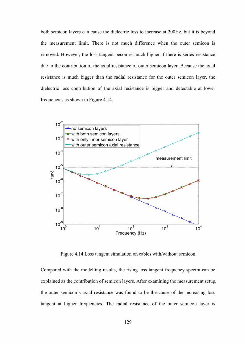
129
both semicon layers can cause the dielectric loss to increase at 200Hz, but it is beyond
the measurement limit. There is not much difference when the outer semicon is
removed. However, the loss tangent becomes much higher if there is series resistance
due to the contribution of the axial resistance of outer semicon layer. Because the axial
resistance is much bigger than the radial resistance for the outer semicon layer, the
dielectric loss contribution of the axial resistance is bigger and detectable at lower
frequencies as shown in Figure 4.14.
100
101
102
103
10410
-9
10-8
10-7
10-6
10-5
10-4
10-3
10-2
Frequency (Hz)
tan δ
no semicon layerswith both semicon layerswith only inner semicon layerwith outer semicon axial resistance
measurement limit
Figure 4.14 Loss tangent simulation on cables with/without semicon
Compared with the modelling results, the rising loss tangent frequency spectra can be
explained as the contribution of semicon layers. After examining the measurement setup,
the outer semicon’s axial resistance was found to be the cause of the increasing loss
tangent at higher frequencies. The radial resistance of the outer semicon layer is

130
calculated as 0.016Ω for a 5m length cable with the resistivity of 10Ωm. This resistance
is too small to account for a contribution to the dielectric loss in this frequency range.
There is a peak related to this small resistance but at very high frequencies that are out
of the measurement frequency range in this study. But if the outer semicon layer is
treated as an electrode, most of the current signal flowing into the measurement
equipment will have to cross the surface resistance, except at the point where the signal
is picked up on the cable sample. This surface resistance is in the range from kΩ to MΩ,
which is big enough to make the loss peak occur at low frequency range below kHz.
The underlying mechanism from the equivalent circuit explanation is that the outer
semicon’s surface resistance will take more voltage drop on it as a mainly resistive
component while the insulation layer is mainly capacitive whose impedance becomes
smaller at higher frequencies. Therefore, the outer semicon layer can contribute and
dominate the loss part when the outer semicon is treated as measuring electrode.
The cable insulation, PE or XLPE, has been widely studied with extracted film samples
from XLPE cables, but the loss of a whole cable is difficult to measure because of the
reasons mentioned in chapter 2. In the a publication of audio-frequency dielectric
spectroscopy on 15kV XLPE cables, Das-Gupta [71] observed increasing dielectric loss
behaviour at room temperature, as shown in Figure 4.15. As the 40cm cable sample was
put into a tap water filled tank as measuring electrode, the resistance of water played the
role as the outer semicon axial resistance in this research study. The author also realized
that this potential high frequency peak is due to the water electrode [71]. In this research
study, the model power cables produced by Borealis were measured with the
transformer ratio bridge system. Similarly, the dielectric loss at 30˚C and 80˚C has an
increasing loss tangent, which is dependent on the resistivity of the semicon materials.

131
The loss tangent spectra are slightly higher than that of Das-Gupta, which was made
under room temperature.
102
103
104
10510
-4
10-3
10-2
10-1
frequency (Hz)
tan δ
Room Temperature, Das-Gupta30C with outer semicon axial resistance, T. Liu80C with outer semicon axial resistance, T. Liu
Figure 4.15 Comparison of loss tangent spectra with the results of Das-Gupta
With the cable samples fully wrapped with conductive adhesive tapes, measurements
were taken on all cables again to avoid the influence of axial resistance of the outer
semicon layer. A comparison using the homo-polymer cable AAA can be seen in Figure
4.16. Two temperatures are chosen for the comparison. It can be seen that the loss
tangent is smaller with copper tape electrode. There is a loss peak in the lower
frequency range, and this is might be due to relaxation process or brought by
instrumental effect. At higher frequencies, cable sample with copper electrode has
decreasing loss tangent at 40°C. This sharp contrast to the previous results further
proves that the increasing loss originates from the axial resistance of the outer semicon

132
layer. However, at higher temperatures when the resistivity of semicon material
becomes bigger, the radial resistance of both semicon layers will still give rise to the
dielectric loss and finally dominate the loss tangent with a slope of 1 while the
conduction loss contribution is relatively much smaller with a slope of -1. In conclusion,
the axial resistance of power cable outer semicon shield is a source of dielectric loss and
brings increasing loss at higher frequencies. Good contact using conductive copper tape
to wrap the cable samples can prevent the influence of axial resistance of outer semicon
layer, as implied in equivalent circuit modelling results as well. This outcome suggests
that metallic shielding outside the outer semicon layer is important in reducing the
dielectric loss in power cable manufacturing.
103
10410
-5
10-4
10-3
10-2
Frequency (Hz)
tan δ
40C, semicon electrode80C, semicon electrode40C, copper electrode80C, copper electrode
Figure 4.16 Comparison of the results from different sample preparation methods.
(copper electrode: solid lines, semicon electrodes: dotted lines)

133
4.3 Dielectric response with discharging current measurement
4.3.1 Temperature dependent discharging current of different cables
The discharging current of cable AAA, ABA and ACA was measured with the
experimental system developed in chapter 3. Before measuring the cable samples, the
“air” cable was measured in comparison with cable AAA in order to check that the
system background does not influence the measurement results on the model cables.
The results are shown in Figure 4.17. During the measuring time of 50ms, cable AAA
has more than 10 times the current than that of the “air” cable. The discharging current
of the “air” cable decayed very quickly in several ms, and it is always neglegible
compared to the discharging current of cable AAA. This result further confirmed that
the discharging current experiemental system can correctly measure the discharging
current of these low loss model power cables. Because the purpose of this measurement
was to study the influence of measurement system on the cable sample measurement in
the short time, a higher range of the electrometer was used. This can reduce the
sensitivity of the system. As it can be seen in Figure 4.17, the noise floor is 10-8A with
the range of 10-5A/V on the current voltage converter. For the measurement on the
model power cables, different ranges were used for different time periods, since the
discharging current decays for more than five decades in only 10 seconds time. The
results of different ranges were merged together for better accuracy.

134
0 0.01 0.02 0.03 0.04 0.0510
-10
10-9
10-8
10-7
10-6
10-5
10-4
10-3
time (s)
curr
ent (
A)
air cablemodel power cable (AAA)
noise floor for higher range ofthe current-voltage converter
Figure 4.17 Comparison of discharging current between the “air” cable and cable AAA
The discharging curent of cable AAA under different temperatures is shown in Figure
4.18. The measurement duration is 13.5s with sampling rate of 1000 sample/second.
The discharging current of homo-polymer cables decayed very quickly. The noisy
current )(tI at longer time was fitted with a power law or Curie-Von-Schweidler law,
nAttI −=)( Equation 4-14
which was proved to be able to represent the multi-relaxation processe of polymer
materials [135] [136] [137]. A and n in Equation 4-14 are fitting parameters. In the
beginning at 20˚C, the discharging current was more than 1.62×10⁻⁶A. The current
decayed linearly in log-log coordinates until several milli-seconds, when there is a small
turning point with another linear decay. The current becomes noisy when it decayed
below 10-11A. Under higher temperatures, the discharging currents are parallel to that of

135
20˚C. The lowest discharging current occurred at 60˚C and it increases at 80˚C. When
the time is longer than about 1s, the discharging currents drop below 10-10A. There is a
trend that in the beginning the discharging current drops faster at higher temperatures
but at longer time the current at higher temperatures drops slower with a smaller slope.
10-3
10-2
10-1
100
10110
-12
10-10
10-8
10-6
time (s)
curr
ent (
A)
20oC
40oC
60oC
80oC
Figure 4.18 Discharging current of cable AAA
Another homo-polymer cable ABA has almost the same discharging current as cable
AAA. In comparison with the homo-polymer cables of AAA and ABA, the co-polymer
cable ACA has overall higher discharging currents at all temperatures, as shown in
Figure 4.19. The discharging current is about 4×10-11A, above the noise floor without
data smoothing. The current at 20˚C is still the highest within the first 10ms. During this
time the temperature dependence is the same as the homo-polymer cables with the
lowest discharging current at 60˚C. However, the discharging current increases at longer

136
times at higher temperatures. It is noticeable that at 80˚C, the discharging current
became almost flat in the last 8s.
10-3
10-2
10-1
100
10110
-11
10-10
10-9
10-8
10-7
10-6
10-5
time (s)
curr
ent (
A)
20oC
40oC
60oC
80oC
Figure 4.19 Discharging current of cable ACA
In summary, the discharging current decays from about 10-6A at 1ms to about 10-12A for
homo-polymer cables and above 10-11A for co-polymer cables. All homo-polymer
cables, AAA and ABA, and co-polymer cable ACA have the highest discharging
currents at 20˚C in the beginning several milli-second. At longer time, the discharging
currents of all cables basically follows the power law (Curie-von Schweidler law) decay,
which is typical for solid dielectrics [70] [137] [138] [139]. However, different
processes can be found especially from the temperature dependence. While the
discharging current has a minimum magnitude at 60˚C in the beginning 10ms, it has
longer decaying trend at higher temperatures at longer time. Higher discharging current
for cable ACA indicates that the co-polymer insulation has higher dielectric loss than

137
that of homo-polymer XLPE insulation. More charge can be stored inside the cable
insulation system, and it takes longer time to discharge when being earthed. This result
is in accordance with the other two frequency domian dielectric spectroscopy
techniques and will be further studied after Fourier transform.
4.3.2 Transformation of discharging current into frequency spectra
Fourier transform is needed to transfer the time domain discharging current data into
frequency domain so that the spectra can be merged together with the results by other
frequency domain techniques. The complex permittivity ∗ε can be calculated with the
following equation [75]
000
)(1CGjdtetI
UCtj
ωεε ω −+= ∫
∞−
∞∗ Equation 4-15
where ∞ε is the high frequency permittivity, 0C is the geometric capacitance of the
measured sample and U is the applied step voltage. ∫∞
−
0
)( dtetI tjω is the Fourier
transform for the measured time dependent current )(tI . It is necessary to include ∞ε as
the Fourier transform only results in the dielectric increment. The term 0C
Gjω
represents any conduction loss contribution in frequency domain. As there is no
conduction in the discharging process, the equation should be rewritten as
∫∞
−∞
∗ +=00
)(1 dtetIUC
tjωεε Equation 4-16

138
This continuous transform is impractical in real applications while the data is digitized
as discrete signal. Discrete Fourier transform (DFT) should be used for the transform. In
order to restore correctly the complex permittivity, the discrete Fourier transform
algorithm is studied in MATLAB environment [140]. When the equation for forward
DFT is
1-0,1,2...Nk )()(1
0
2
== ∑−
=
−N
n
nkN
j
enxkXπ
Equation 4-17
where )(nx is the time domain series, )(kX is the frequency domain series, )(kX
should be divided by N (number of DFT points) to give the correct real and imaginary
permittivity values. The final equation under discharging condition for calculating
discrete frequency domain complex permittivity is
1,2,3...Nk )(1)(10
2
=′′−Δ+=+= ∞=
∞∗ ∑
−
εεεεεπ
jenxUNC
kN
n
nkN
j
Equation 4-18
Using the DFT algorithm, the complex permittivity for the discharging current data on
the model power cables can be calculated and their loss tangent were obtained by
)()(tan
kk
εεδ′′′
= Equation 4-19
Using Equation 4-18, the imaginary permittivity ε'' and the real permittivity increment
Δε' have been calculated. Excluding the data that has the influence truncation error, the
frequency spectra from 1Hz to 100Hz for the model power cables were obtained. The ε''
of cable AAA is shown in Figure 4.20, with 1f and -1f to help determine the types of
relaxation. The ε'' of all temperatures ranges from 10-6 to 10-4. Such low loss cannot be
measured by the frequency domain techniques – FRA and bridges. The ε'' at 20°C is the

139
biggest in this whole frequency range with its maximum value of 4.80×10⁻⁵ at 100Hz.
The ε'' decreases at higher temperatures until 60°C, which has the minimum value of
8.96×10⁻⁶ at 2Hz. The ε'' increases again at 80°C with the values between those of 20°C
and 60°C. This temperature dependence, which has a minimum dielectric loss at 60°C,
has been found in the depolarization current for all the XLPE model power cables.
There is no loss peak in this frequency range at all temperatures. Compared with the
slope of -1 and 1, the dielectric loss of cable AAA does not have a Debye type loss and
it has a very flat dielectric loss especially at lower temperatures, which suggests
multiple relaxations typical for solid polymers. It is also noticeable that there is a slope
at higher temperatures of 60°C and 80°C at lower frequencies. Although the slope is
still smaller than -1, this may indicate an extra broad relaxation process is shifting
towards higher frequencies at higher temperature.
10-1
100
101
10210
-6
10-5
10-4
frequency (Hz)
ε''
20oC
40oC
60oC
80oC
f-1 f1
Figure 4.20 ε'' of cable AAA under different temperatures,
transformed from the discharging current

140
The real permittivity increment Δε' of cable AAA is shown in Figure 4.21. The
increment represents the deviation from the high frequency real permittivity ∞ε , i.e. the
frequencies above those that are being observed by this technique. Similar to the ε''
results, the biggest increment happens at 20°C with maximum Δε'=5.27×10⁻⁴ at the
lowest frequency end 0.15Hz and the smallest at 60°C with maximum Δε'=2.67×10⁻⁴.
For all temperatures, the Δε' decreases smoothly at higher frequencies. It is noticeable
that the Δε' is negligible with the values at the order of 10-4, comparing the value of
2.18±0.04 measured using the transformer ratio bridge for the ∞ε of polyethylene.
However, the Δε' has the advantage of analyzing the relaxation behaviour more clearly.
With the pure permittivity increment at 20°C, it can be seen that the increment of Δε' in
this frequency range is 2.67×10⁻⁴. This very small real permittivity increment indicates
there is a very broad loss peak.
10-1
100
101
1022
2.5
3
3.5
4
4.5
5
5.5x 10⁻⁴
frequency (Hz)
Δε'
20oC
40oC
60oC
80oC
Figure 4.21 Δε' of cable AAA under different temperatures,
transformed from the discharging current

141
Considering the average value for high frequency permittivity 18.2=∞ε for cable AAA,
the real permittivity has been calculated
)(18.2 ωεεεε ′Δ+=′Δ+=′ ∞ Equation 4-20
The loss tangent was then calculated with Equation 4-19, and it is shown in Figure 4.22.
The shapes of the tanδ at higher frequencies with all temperatures are the same as the ε''
in Figure 4.20, because the Δε' is so small that it does not bring too much increment to
the ε'. The loss tangent of this homo-polymer cable has very low polarization loss,
ranging from 2.2×10⁻⁶ to 4.0×10⁻⁵ in general. Practical importance can be considered at
50Hz. At this mains frequency, the loss tangent due to pure polarization for the cables
has the lowest value at 60°C.
10-1
100
101
10210
-6
10-5
10-4
frequency (Hz)
tan δ
20oC
40oC
60oC
80oC
f-1
Figure 4.22 Loss tangent of cable AAA under different temperatures,
transformed from the discharging current
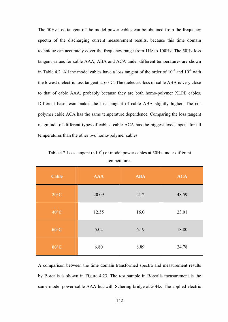
142
The 50Hz loss tangent of the model power cables can be obtained from the frequency
spectra of the discharging current measurement results, because this time domain
technique can accurately cover the frequency range from 1Hz to 100Hz. The 50Hz loss
tangent values for cable AAA, ABA and ACA under different temperatures are shown
in Table 4.2. All the model cables have a loss tangent of the order of 10-5 and 10-6 with
the lowest dielectric loss tangent at 60°C. The dielectric loss of cable ABA is very close
to that of cable AAA, probably because they are both homo-polymer XLPE cables.
Different base resin makes the loss tangent of cable ABA slightly higher. The co-
polymer cable ACA has the same temperature dependence. Comparing the loss tangent
magnitude of different types of cables, cable ACA has the biggest loss tangent for all
temperatures than the other two homo-polymer cables.
Table 4.2 Loss tangent (×10-6) of model power cables at 50Hz under different
temperatures
Cable AAA ABA ACA
20°C 20.09 21.2 48.59
40°C 12.55 16.0 23.01
60°C 5.02 6.19 18.80
80°C 6.80 8.89 24.78
A comparison between the time domain transformed spectra and measurement results
by Borealis is shown in Figure 4.23. The test sample in Borealis measurement is the
same model power cable AAA but with Schering bridge at 50Hz. The applied electric

143
field is 25kV/mm with the temperatures of 25°C, 60°C, 90°C and 100°C. It can be seen
that the 50Hz loss tangent by both techniques have the same trend at different
temperatures. The highest loss tangent occurred at lower temperatures and the lowest at
60°C for both techniques. The reason for higher loss tangent values in Borealis
measurement results is due to higher applied electric field. The high field dependence
has also been studied in this research work and will be introduced in chapter 5. Another
reason is that the loss tangent spectra in this study were transformed data from
discharging currents without the contribution of conduction loss.
20 30 40 50 60 70 80 90 10010
-6
10-5
10-4
10-3
temperature (oC)
tan δ
1kV/1.5mm, this work25kV/mm, measured by Borealis
Figure 4.23 Loss tangent of cable AAA at 50Hz,
compared with measurement results by Borealis

144
4.4 Master curve in the frequency range from 10‐4Hz to 104Hz
4.4.1 Data combination of different techniques
The measurement results of the three techniques are in different frequency ranges that
makes it possible to show a broader loss tangent spectrum from 10-4Hz to 104Hz. With
the measurement results of real and imaginary permittivity, the loss tangent for FRA
can be calculated by Equation 4-19. The results for cable ABA is shown in Figure 4.24.
The results of different temperatures are shown in the same graph but the loss tangent is
too small and in the noise floor at lower temperatures and higher frequencies. Because ε'
does not change for cables AAA and ABA, the shapes of tanδ is the same as that of ε'',
shown in Figure 4.4. The magnitudes are decreased by the factor of the ε'. Valid tanδ
values at 10-4Hz can be found for 60°C and 80°C as 1.20×10⁻² and 1.83×10⁻¹
respectively. This very low frequency loss can well represent the DC conductivity loss
and it mainly originates from the conduction current.
Figure 4.25 shows the loss tangent spectrum for cable ACA. The results have slightly
different shapes from ε'' because ε' has substantial increment, e.g., ε' increased 0.8 from
2.36 at 1Hz to 3.16 at 10-4Hz under 80°C as shown in Figure 4.5. Apart from the DC
conductivity loss with slope of -1, the additional loss peaks at 60°C and 80°C that relate
to ε' increment are more obvious. The tanδ of cable ACA is the biggest, compared with
cables AAA and ABA. At the frequency of 10-4Hz, tanδ is 1.55×10⁻¹ at 60°C and
7.08×10⁻¹ at 80°C, which are 13 times and 4 times bigger than those for cable ABA.
Smaller difference at 80°C implies that the dielectric loss increases faster with
increasing temperature and higher thermally activated conduction for homo-polymer
cable ABA.
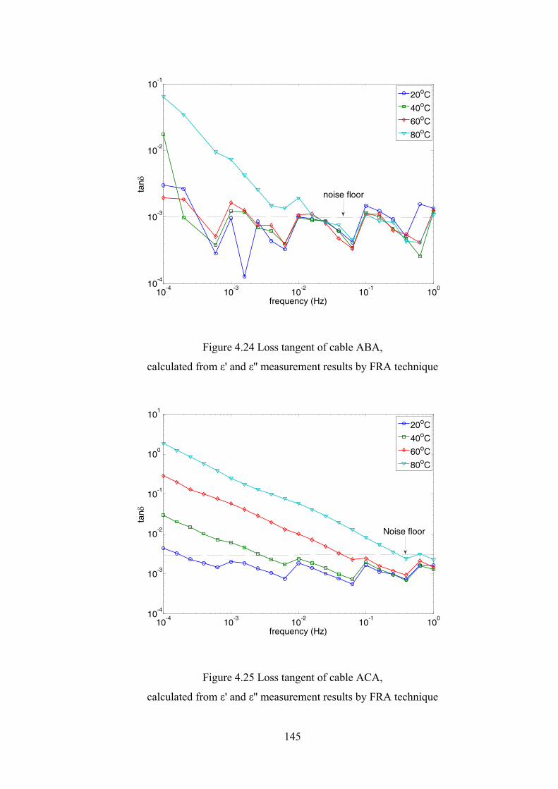
145
10-4
10-3
10-2
10-1
10010
-4
10-3
10-2
10-1
frequency (Hz)
tan δ
20oC
40oC
60oC
80oC
noise floor
Figure 4.24 Loss tangent of cable ABA,
calculated from ε' and ε'' measurement results by FRA technique
10-4
10-3
10-2
10-1
10010
-4
10-3
10-2
10-1
100
101
frequency (Hz)
tan δ
20oC
40oC
60oC
80oC
Noise floor
Figure 4.25 Loss tangent of cable ACA,
calculated from ε' and ε'' measurement results by FRA technique

146
In the middle frequency range, the frequency spectra from discharging current can cover
the range from 0.1Hz to 100Hz. The transformation from time domain into frequency
domain has been introduced in Section 4.3.2 with Equation 4-18. The loss tangent in
Figure 4.22 shows the dielectric loss of cable AAA without conduction loss contribution,
because the discharging current only includes depolarization of the insulation. In order
to conform to the other two frequency domain techniques that measure the dielectric
loss including the conduction loss contribution, the conduction loss should be added
based on the conductivity measurement results. The conduction loss contribution to the
ε'' was calculated with the measurement data on air degassed model power cables in
Section 4.5 by
02 επσεf
=′′ Equation 4-21
Figure 4.26 shows ε'' of cable ACA. The straight lines with slope of -1 represent the DC
conductivity loss measured from steady state current during charging process. The line
of 20°C is outside of the graph scales. After adding the conduction contribution, the
depolarization loss from discharging current was greatly increased at lower frequencies
and higher temperatures. The total dielectric loss has been plotted with solid marker
lines. Compared with the depolarization loss, there is no observable difference at 20°C
because the conduction loss contribution is so small. As the temperature increases, the
conduction loss starts to dominate the dielectric loss, and determines the shape of the
lower frequency tanδ spectra.
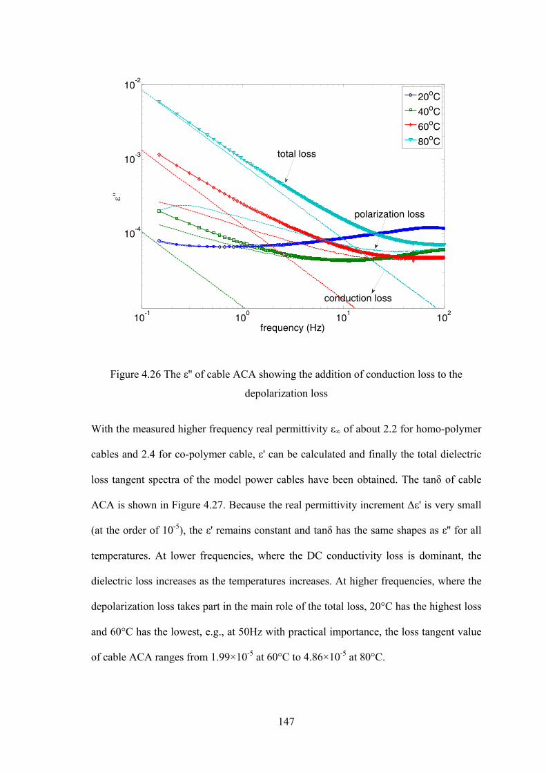
147
10-1
100
101
102
10-4
10-3
10-2
frequency (Hz)
ε''
20oC
40oC
60oC
80oC
polarization loss
total loss
conduction loss
Figure 4.26 The ε'' of cable ACA showing the addition of conduction loss to the
depolarization loss
With the measured higher frequency real permittivity ε∞ of about 2.2 for homo-polymer
cables and 2.4 for co-polymer cable, ε' can be calculated and finally the total dielectric
loss tangent spectra of the model power cables have been obtained. The tanδ of cable
ACA is shown in Figure 4.27. Because the real permittivity increment Δε' is very small
(at the order of 10-5), the ε' remains constant and tanδ has the same shapes as ε'' for all
temperatures. At lower frequencies, where the DC conductivity loss is dominant, the
dielectric loss increases as the temperatures increases. At higher frequencies, where the
depolarization loss takes part in the main role of the total loss, 20°C has the highest loss
and 60°C has the lowest, e.g., at 50Hz with practical importance, the loss tangent value
of cable ACA ranges from 1.99×10⁻⁵ at 60°C to 4.86×10⁻⁵ at 80°C.

148
10-1
100
101
102
10-4
10-3
10-2
frequency (Hz)
tan δ
20oC
40oC
60oC
80oC
Figure 4.27 Loss tangent spectra of cable ACA at different temperatures
The transformer ratio bridge measurement results cover the frequency range from
300Hz to 10kHz. With the measured capacitance and conductance, Equation 4-4 was
used for the loss tangent calculated of all the tested model power cables. After using the
conductive adhesive copper tapes to wrap the whole length of the cable samples, the
extra loss brought by axial resistance of the outer semicon layer has been largely
eliminated. The loss tangent spectra of cable AAA under four temperatures are shown
in Figure 4.28. The tanδ ranges from 10-5 to 10-2. In the lower frequency range, there is
a loss peak at 200Hz. Because this loss peak is independent of temperatures, it might be
due to instrument errors. The loss tangent can be distinguished at higher frequencies. It
increases at higher temperatures. Increasing loss with slope of 1 can be seen at 60°C and
80°C. The loss tangent at 10kHz is 4.06×10⁻⁴ at 60°C and 1.37×10⁻³ at 80°C. At 20°C,
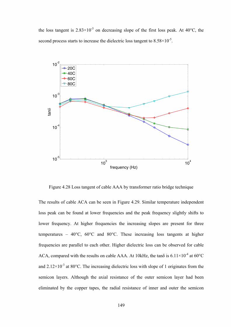
149
the loss tangent is 2.83×10⁻⁵ on decreasing slope of the first loss peak. At 40°C, the
second process starts to increase the dielectric loss tangent to 8.58×10⁻⁵.
103
10410
-5
10-4
10-3
10-2
frequency (Hz)
tan δ
20C40C60C80C
Figure 4.28 Loss tangent of cable AAA by transformer ratio bridge technique
The results of cable ACA can be seen in Figure 4.29. Similar temperature independent
loss peak can be found at lower frequencies and the peak frequency slightly shifts to
lower frequency. At higher frequencies the increasing slopes are present for three
temperatures – 40°C, 60°C and 80°C. These increasing loss tangents at higher
frequencies are parallel to each other. Higher dielectric loss can be observed for cable
ACA, compared with the results on cable AAA. At 10kHz, the tanδ is 6.11×10⁻⁴ at 60°C
and 2.12×10⁻³ at 80°C. The increasing dielectric loss with slope of 1 originates from the
semicon layers. Although the axial resistance of the outer semicon layer had been
eliminated by the copper tapes, the radial resistance of inner and outer the semicon

150
layers will give increase to the loss tangent at higher frequencies. In the equivalent
circuit, even a very small series resistance will cause the loss tangent to increase at high
frequencies. Because the conductivity of semicon materials decreases with increasing
temperatures in the range from 20°C to 90°C, making the semicon layers more resistive,
the values of the increasing loss tangent become bigger at higher temperatures. The
reason for cable ACA to have higher dielectric loss is that additional dielectric loss
origins, e.g. the polarization of the micron-size ethylene-butyl-acrylate islands for this
co-polymer cable, have higher contribution to the total dielectric loss than the homo-
polymer cables.
103
10410
-5
10-4
10-3
10-2
frequency (Hz)
tan δ
20oC
40oC
60oC
80oC
Figure 4.29 Loss tangent of cable ACA by transformer ratio bridge technique
The results of cable BAB are shown in Figure 4.30, in order to compare the effects of
different semicon materials. with semicon B – super-smooth semicon, the overall loss
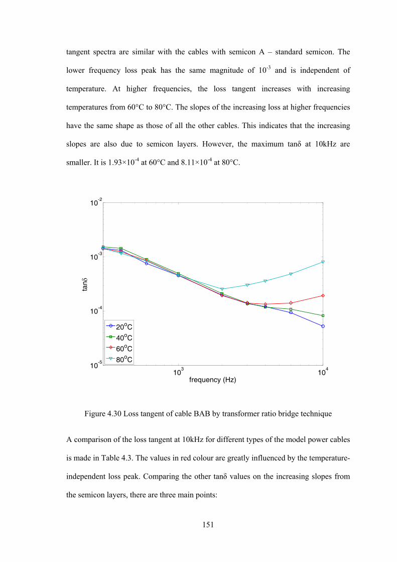
151
tangent spectra are similar with the cables with semicon A – standard semicon. The
lower frequency loss peak has the same magnitude of 10-3 and is independent of
temperature. At higher frequencies, the loss tangent increases with increasing
temperatures from 60°C to 80°C. The slopes of the increasing loss at higher frequencies
have the same shape as those of all the other cables. This indicates that the increasing
slopes are also due to semicon layers. However, the maximum tanδ at 10kHz are
smaller. It is 1.93×10⁻⁴ at 60°C and 8.11×10⁻⁴ at 80°C.
103
10410
-5
10-4
10-3
10-2
frequency (Hz)
tan δ
20oC
40oC
60oC
80oC
Figure 4.30 Loss tangent of cable BAB by transformer ratio bridge technique
A comparison of the loss tangent at 10kHz for different types of the model power cables
is made in Table 4.3. The values in red colour are greatly influenced by the temperature-
independent loss peak. Comparing the other tanδ values on the increasing slopes from
the semicon layers, there are three main points:

152
1) Cable AAA has very close dielectric loss to that of cable ABA. This suggests
that these two homo-polymer cables with the same semicon material have the
dominant loss tangent from semicon layers at higher frequencies, while their
dielectric loss from the insulation material – XLPE – is not detectable.
Table 4.3 Loss tangent (×10-5) of the model power cables at 10kHz under different
temperatures, measured with transformer ratio bridge technique (the values in red
colour are mainly due to instrument errors rather than due to the semicon resistance)
Cable AAA ABA ACA BAB
20°C 2.83 3.73 7.87 5.28
40°C 8.58 8.30 18.9 8.20
60°C 40.6 42.1 61.1 1.93
80°C 137 130 212 81.1
2) Cable ACA with co-polymer insulation layer has higher dielectric loss than the
other homo-polymer cables. The increasing slope can be observed at 40°C. This
implies that the co-polymer insulation contribute additional dielectric loss that
may be due to the polarization of small polar molecules - the micron-size
ethylene-butyl-acrylate.
3) Cable BAB with different semicon layers has lower dielectric loss than cable
AAA. Since the loss should be mainly from the semicon layers, with the
knowledge of the equivalent circuit modelling, this indicates that semicon B has
higher conductivity or smaller resistivity in this temperature range, which can be

153
proved by the measurement results on the conductivity of semicon materials in
Section 4.2.
4.4.2 Loss tangent master curves
The loss tangent results by all three dielectric spectroscopy techniques may be merged
together. The extrapolated master curves covering a wide frequency range from 10-4Hz
to 104Hz can be obtained. The extrapolation of master curve for cable AAA is shown in
Figure 4.31. The original results of three techniques are plotted separately in different
frequency ranges. The data in noise floor and instrumental errors should be excluded
from this extrapolation process. The thick dashed black lines show the master curves for
60°C and 80°C. A dashed line with slope of 1 is plotted to help analyze the higher
frequency spectra. The loss tangent due to DC conductivity at different temperatures
with slope of -1 is also plotted to compare with FRA data and to help explain lower
frequency spectra. Because of the measurement accuracy limitations, only at 60°C and
80°C can the master curve be extrapolated for the whole frequency range. At lower
frequencies from 10-4Hz to 1Hz, the FRA results can be merged with the TDDS results,
assuming a smooth transition in the range from 10-2 to 10-1Hz in which there is no valid
measurement data. The merging between TDDS results and transformer bridge results
should consider the possible instrumental effects that bring a Debye loss peak at the
beginning. Therefore, the master curve only connects the second process of the
increasing loss in transformer bridge results. From the master curve of cable AAA at
80°C, it can be seen that at lower frequencies, conduction loss with slope of -1
dominates the dielectric loss in the frequency range from 10-4Hz to 10-1Hz. Then, the
absolute value of the slope becomes less than 1. In the range 10-1Hz to 100Hz, the
dielectric loss is rather “flat” with different temperature dependence as found in

154
previous sections. This suggests multiple loss behaviour is present. At higher
frequencies, the dielectric loss due to semicon layers dominates with slope of 1.
10-4
10-2
100
102
10410
-6
10-5
10-4
10-3
10-2
10-1
frequency (Hz)
tan δ
20oC
40oC
60oC
80oC
f1DC conduction f-1
FRA
Transformer bridge
TDDS
Figure 4.31 Extrapolation of master curve for cable AAA
from measurement results of three dielectric spectroscopy techniques
In conclusion, cable AAA has multiple loss origins. Its dielectric loss tangent is from
10-6 to 10-1 in the frequency range from 10-4Hz to 104Hz. The most remarkable feature
for its dielectric loss spectrum is that conduction loss dominates lower frequencies
while semicon layers dominate higher frequencies. The lowest dielectric loss occurs at
the middle frequencies from 1Hz to 100Hz. In this frequency range, the intrinsic
polarization loss of the XLPE cable insulation can be identified.
Cable ACA with co-polymer insulation has the highest dielectric loss, as found in all
three techniques. The master curves for all temperatures have been extrapolated, as

155
shown in Figure 4.32. At lower frequencies, conduction loss is dominant and its spectra
are parallel. The increasing loss with increasing temperatures indicates that the DC
conductivity of the model power cables is thermally activated. At 60°C and 80°C, there
is an additional loss peak overlapping with the DC conductivity loss. This additional
loss is due to polarization because a relevant real permittivity increment was found in
FRA measurement as discussed in Section 4.1.2. From 1Hz to 1kHz, the temperature
dependence changes, e.g., 20°C has the highest loss tangent. Loss behaviour other than
DC conductivity or semicon resistance is dominant, while the DC conductivity loss
slope of -1 and semicon loss slope of 1 both attenuate to negligible magnitudes. At
higher frequencies, semicon layers produce most of the dielectric loss with increasing
loss at higher temperatures.
10-4
10-2
100
102
104
10-4
10-3
10-2
10-1
100
101
frequency (Hz)
tan δ
20oC
40oC
60oC
80oC
f1DC conduction f-1
FRA
Transformer bridge
TDDS
Figure 4.32 Extrapolation of master curve for cable ACA
from measurement results of three dielectric spectroscopy techniques

156
4.5 Effect of degassing by conduction current measurement
The effects of degassing were studied on the conductivity of the model power cables
using DC conduction current measurement. In order to achieve higher accuracy, the
“harmonic-free” battery supply was used with Keithley electrometer model 617. Three
different types of the model power cables – AAA, ABA and ACA have been tested
under non-degassed fresh, air degassed and vacuum degassed conditions. The DC
conductivity of those cables under different temperatures will be studied to characterise
the degassing effects.
4.5.1 Time delay for conduction measurement
Because polymeric insulation materials have long chain molecules and take longer time
to be polarized, the pure DC conduction current should be measured with a time delay
for the insulation to be charged. With the purpose of finding out the time delay for DC
conduction current measurement, the charging current for cable AAA and cable ACA
was measured and the results are shown in Figure 4.33. The measurement was taken
from 10-3 hour to more than 100 hours with irregular time intervals. For cable AAA, the
charging current is 2.71×10⁻¹⁰A at five seconds and decayed to 1.56×10⁻¹²A after two
hours. After four hours the current was 4.68×10⁻¹⁴A, with four decade decay from the
beginning. After four hours, very little decrement can be measured. When the voltage
was applied for twenty one hours, the current was 4.25×10⁻¹⁴A. Only 4.3×10⁻¹⁵A
decaying was measured from four hours to twenty one hours. Cable ACA has similar
decay with a faster charging process. At four hours, the current decayed to 1.96×10⁻¹¹A.
From this time point to the last point at one hundred and forty four hours (six days), the

157
current decayed to 1.86×10⁻¹¹A, with only 1pA decrement. Therefore, four hours time
delay was practically chosen for the DC conduction measurement.
10-3
10-2
10-1
100
101
10210
-13
10-12
10-11
10-10
10-9
time (hour)
curr
ent (
A)
cable AAA, degassedcable ACA, degassed
4 hours
Figure 4.33 Current measurement on cable AAA
in order to find the time delay for DC conduction measurement
4.5.2 Results of non‐degassed, air degassed and vacuum degassed cables
The non-degassed model power cables were firstly tested. Then the cable samples were
degassed in air and in vacuum oven for repeated measurements on the same samples.
The measurement results on fresh cable samples are shown in Figure 4.34. All three
types of cables were measured under four temperatures from 20°C to 80°C. For cable
AAA and ABA at 20°C, reliable data cannot be read because the measurement system
has current measurement limit at 10-13A. All cables have increasing DC conduction
current under increasing temperatures. Cable AAA has the lowest DC conduction
current with a good linear increasing trend in the semi-log scale axis. Cable ABA has

158
higher and parallel DC conduction current, compared with cable AAA. Cable ACA has
the highest DC current with the biggest of 7.09×10⁻⁹A under 80°C for the 5m long
sample.
20 30 40 50 60 70 8010
-13
10-12
10-11
10-10
10-9
10-8
temperature (oC)
curr
ent (
A)
AAA, non-degassedABA, non-degassedACA, non-degassed
Figure 4.34 DC conduction current measurement results
for non-degassed cables of AAA, ABA and ACA
Based on the geometric dimensions of the cable samples, the DC conductance is
)/ln(2
0 irrLG πσ
= Equation 4-22
With Ohm’s law UIG = , the conductivity of the cable insulation can be calculated
LUIrr i
πσ
2)/ln( 0= Equation 4-23

159
20 30 40 50 60 70 8010
-17
10-16
10-15
10-14
10-13
10-12
temperature (oC)
cond
uctiv
ity (
S/m
)
ACA, non-degassedACA, air degassedACA, vacuum degassed
Figure 4.35 Conductivity of cable ACA
with non-degassed, degassed and vacuum degassed conditions
The conductivity before and after degassing for three model power cables – AAA, ABA
and ACA has been calculated from the DC conduction current measurement results. It is
an essential electrical property of insulation materials and independent of dimensions.
Figure 4.35 shows the conductivity of cable ACA under fresh, air degassed and vacuum
degassed conditions. It can be seen from the results that the conductivity decreases after
five days degassing in air. For example at 40°C, the conductivity decreases from
1.47×10⁻¹⁵S/m to 5.85×10⁻¹⁶S/m with 60.17% decrement. Further decrement was
measured after another five days degassing in vacuum oven with 10-3bar (approximately
10-3atm). At 40°C, the conductivity decreases to 4.64×10⁻¹⁶S/m with 68.35% decrement
from the fresh condition and with further 20.55% decrement from the air degassed
condition. The conductivity of different conditions is parallel to each other and
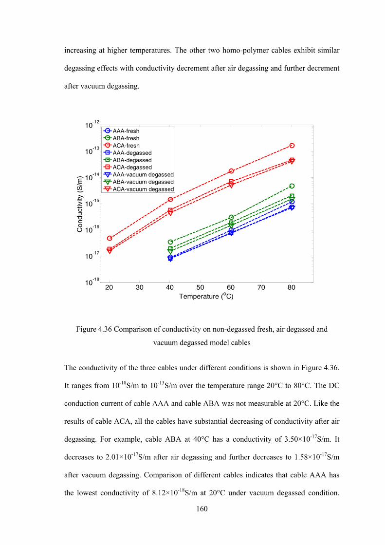
160
increasing at higher temperatures. The other two homo-polymer cables exhibit similar
degassing effects with conductivity decrement after air degassing and further decrement
after vacuum degassing.
20 30 40 50 60 70 8010
-18
10-17
10-16
10-15
10-14
10-13
10-12
Temperature (oC)
Con
duct
ivity
(S
/m)
AAA-freshABA-freshACA-freshAAA-degassedABA-degassedACA-degassedAAA-vacuum degassedABA-vacuum degassedACA-vacuum degassed
Figure 4.36 Comparison of conductivity on non-degassed fresh, air degassed and
vacuum degassed model cables
The conductivity of the three cables under different conditions is shown in Figure 4.36.
It ranges from 10-18S/m to 10-13S/m over the temperature range 20°C to 80°C. The DC
conduction current of cable AAA and cable ABA was not measurable at 20°C. Like the
results of cable ACA, all the cables have substantial decreasing of conductivity after air
degassing. For example, cable ABA at 40°C has a conductivity of 3.50×10⁻¹⁷S/m. It
decreases to 2.01×10⁻¹⁷S/m after air degassing and further decreases to 1.58×10⁻¹⁷S/m
after vacuum degassing. Comparison of different cables indicates that cable AAA has
the lowest conductivity of 8.12×10⁻¹⁸S/m at 20°C under vacuum degassed condition.

161
Cable ACA has the highest conductivity. This suggests that homo-polymer cable
insulation is better than co-polymer cable insulation because the conductivity of co-
polymer cable ACA has much higher conductivity than cable AAA and ABA.
The degassing level in average percentage of temperatures from the non-degassed fresh
condition to air and vacuum degassed conditions is shown in Table 4.4. For cable AAA,
the degassing in the air can reduce its conductivity for 23.46%. Further degassing in
vacuum oven only improved 0.8%. Cable ABA has conductivity decrement of 45.30%
after air degassing with 12.76% by further vacuum degassing. Cable ACA has the
biggest conductivity decrement of 62.79% after air degassing with 7.15% by further
vacuum degassing, compared with the other two homo-polymer cables.
Table 4.4 Average percentage of conductivity decrement
after air and vacuum degassing for three model power cables
Cable AAA ABA ACA
Fresh air degassed 23.5% 45.3% 62.8%
Fresh vacuum degassed 24.3% 58.0% 70.0%
In conclusion, degassing process can decrease the DC conductivity of the model power
cables and, therefore, improve the insulation performance by reducing the dielectric loss.
All model power cables have large amount of decrement from 23.46% to 62.79% after
air degassing. Volatile by-products and impurities in fresh cables can be effectively
removed by the degassing process so that the concentration of conductive charge
carriers can be reduced. Further improvement can be made by using vacuum oven for
the degassing procedure, but air degassing is more practical for mass production.

162
Comparatively, homo-polymer cables have smaller conductivity decrement after
degassing. Cable AAA has the least degassing effect, while cable ABA has the biggest
vacuum degassing effect. The further conductivity decrement after vacuum degassing
may be also due to longer degassing time after air degassing and depend on the control
of peroxide and additives during cable manufacturing.
4.6 Conclusions
Dielectric response of degassed model power cables was measured using FRA,
transformer ratio bridge and TDDS systems:
1. ε'' has slope of -1 and ε' does not change much at lower frequencies from 10-4Hz
to 1Hz, indicating that conduction loss is dominant.
2. The tanδ spectra has slope of 1 at higher frequencies from 102Hz to 104Hz. This
is due to semicon layer resistance, according to the cable equivalent circuit
modelling results.
3. Fourier transformation is used to convert TDDS data into frequency spectrum.
“Flat” loss was found to dominate at the frequency range from 10-1Hz to 102Hz.
4. Degassing effects have been studied using stable state current measurement. It
was found that the conductivity can be reduced by 24% ~ 63% after degassing
process and further reduction may be realized using vacuum degassing.
5. Both the dielectric spectra and DC conductivity of homo-polymer cables is
lower than co-polymer cables.

163
5 Thermal ageing effects on model power cables
The model power cables with different insulation were thermally aged in an oven at
135°C for 50 days. This accelerated ageing condition is suggested by the model cable
manufacturer. Apart from the obvious change of colour after the ageing process, the
dielectric response measurements with FRA and TDDS have been taken to study the
cable’s electrical property changes. The influence of thermal ageing on the conductivity
of the model power cables is also studied. The activation energy of the aged cables, in
comparison with new degassed cables, is calculated based on the Arrhenius plots. In
order to study the dielectric loss tangent of aged power cables under operating
conditions, Schering bridge tests at mains frequency on both new degassed and aged
cables are analyzed.
In chapter 3 and chapter 4, it was shown that the transformer ratio bridge measurement
was greatly dependent on the contact between measuring electrode and outer semicon
layer of the cable samples, so the measurement results are not reported for the aged
cables. The conductivity of polymer power cables due to ageing would be expected to
change [57] [141] [142]. So, the charging and discharging current measurements are
presented in time domain. FRA measurement down to 10-4Hz were presented which
showed the change of conductivity in the imaginary part of the capacitance and also a
change in the real part of complex permittivity. Spectra from 10-4Hz to 102Hz have been
merged together and presented to compare aged and unaged cables using all the above
information. Finally, the ageing effect with higher electric field has been measured with
Schering bridge at 50Hz.

164
5.1 Dielectric response of aged model power cables using FRA
5.1.1 Ageing effect on homo‐polymer model power cables
Experiments with frequency response analyzer under the same testing conditions as the
unaged cables were carried out for different model power cables. Comparison can be
made between the results of aged and unaged cable samples. The comparison of FRA
measurement results for cable AAA is shown in Figure 5.1.
10-4
10-3
10-2
10-1
10010
-4
10-3
10-2
10-1
100
101
frequency (Hz)
20oC
40oC
60oC
80oC
aged cable - solid lineunaged cable - dashed line
ε''
ε'
noise floor
Figure 5.1 Comparison of real permittivity ε' and imaginary permittivity ε'' between
aged and unaged cable AAA, measured with FRA technique at different temperatures
The real permittivity ε' and imaginary permittivity ε'' are plotted in the same graph in
order to judge the types of dielectric loss. All solid lines represent the results of aged
cable with different colours for different temperatures, while dashed lines represent the
results of unaged cable. As found before, unaged cable AAA has the lowest dielectric

165
loss. Its ε'' is only measurable at 80°C; it is below the measurement limit for lower
temperatures. After cable AAA was aged, its ε'' increased from 0.14 to 4.11 at 10-4Hz.
ε'' at 60°C could be measured and was found to be 0.26 at 10-4Hz, even higher than that
of unaged cable at 80°C (ε''=0.14). The ε'' of aged cable AAA at both 60°C and 80°C
has a slope of very close to -1. Considering that ε' does not have a big increment at
lower frequencies, e.g., with parallel negative slope to the ε'', the dielectric loss is
mainly due to DC conductivity.
10-4
10-3
10-2
10-1
1002
2.1
2.2
2.3
2.4
2.5
2.6
frequency (Hz)
ε'
20oC
40oC
60oC
80oC
aged cable - solid lineunaged cable - dashed line
Figure 5.2 Comparison of real permittivity ε' between aged and unaged cable AAA at
different temperatures, showing increment for aged cable at 80°C
Although ε' seems rather constant for both aged and unaged cables in Figure 5.1, ε' of
aged cable AAA at 80°C in fact has considerable increment at lower frequencies, as
shown in Figure 5.2. The comparison of ε' for aged and unaged cables indicates that the
thermal ageing process resulted in its increment at higher temperatures. ε' at 80°C is

166
2.2±0.03 before ageing and increases to 2.45 at 10-4Hz after ageing. This increasing
trend starts at the frequency of 2×10⁻³Hz and has an increment Δε' of 0.25 at 10-4Hz. A
relevant loss peak for possible polarization or increasing loss towards lower frequencies
for quasi-DC should be in the imaginary permittivity ε'', though it is not very obvious
while conduction loss is dominant.
5.1.2 Ageing effect on co‐polymer model power cables
The measurement results on co-polymer cable ACA before and after ageing process are
also compared to study the ageing effects on the dielectric properties. The comparison
of the imaginary permittivity ε'' is shown in Figure 5.3. Because cable ACA has a higher
dielectric loss than the homo-polymer cables, ε'' can be measured for all four
temperatures. ε'' increased after thermal ageing. The increment becomes bigger at higher
temperatures. At 40°C and 10-4Hz, ε'' increases from 1.11×10⁻² to 1.56×10⁻²; at 80°C, ε''
increases from 2.23 to 7.89. ε'' after ageing is not very parallel to slope of -1 indicating
similar loss behaviour. Apart from DC conductivity loss, additional loss peak can be
seen for 60°C and 80°C. These two loss peaks are related to the increment of the real
permittivity ε' at lower frequencies, as shown in Figure 5.4. However, this small
polarization loss is overwhelmed by conduction loss. ε' at 20°C does not have an
apparent increase after the cable is thermally aged. When the temperature increases to
40°C, a small amount of increment can be seen while ε' is constant for unaged cable
ACA. ε'' is curved at 40°C, which implies that a polarization peak is present. For higher
temperatures of 60°C and 80°C, ε' increases further after ageing, e.g., from 3.1 to 3.7 at
80°C.

167
10-4
10-3
10-2
10-1
10010
-3
10-2
10-1
100
101
102
Frequency (Hz)
ε''
20oC
40oC
60oC
80oC
aged cable - solid lineunaged cable - dashed line
f-1
Figure 5.3 Comparison of imaginary permittivity ε'' for aged and unaged cable ACA,
measurement with FRA technique
10-4
10-3
10-2
10-1
1002.2
2.4
2.6
2.8
3
3.2
3.4
3.6
3.8
Frequency (Hz)
ε'
20oC
40oC
60oC
80oC
aged cable - solid lineunaged cable - dashed line
Figure 5.4 Comparison of real permittivity ε' for aged and unaged cable ACA,
measurement with FRA technique
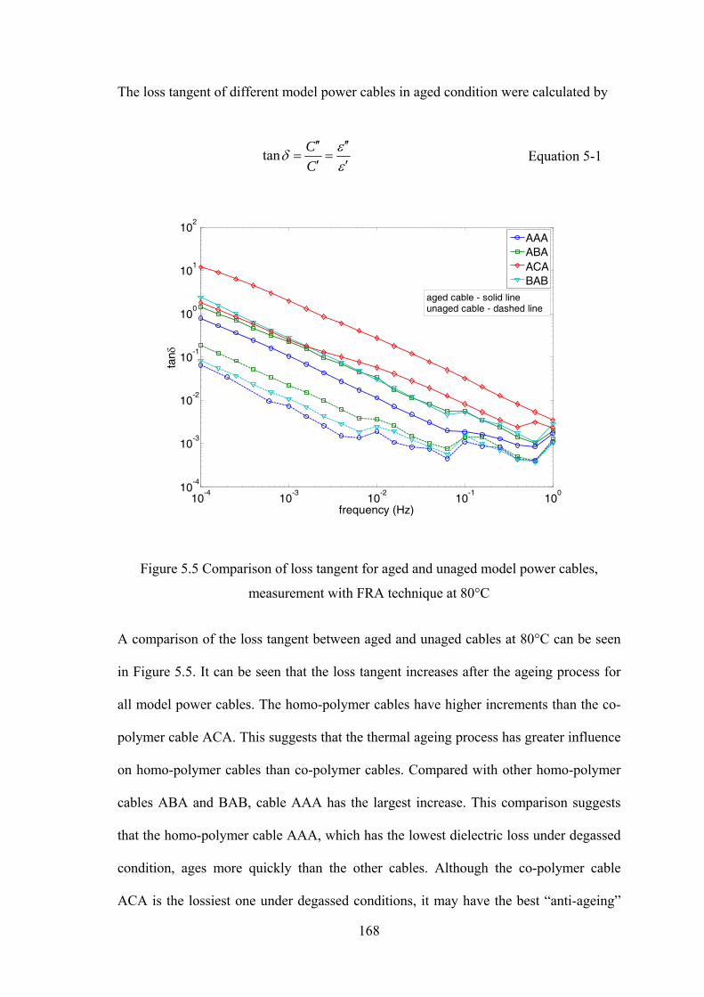
168
The loss tangent of different model power cables in aged condition were calculated by
εεδ′′′
=′′′
=CCtan Equation 5-1
10-4
10-3
10-2
10-1
10010
-4
10-3
10-2
10-1
100
101
102
frequency (Hz)
tan δ
AAAABAACABAB
aged cable - solid lineunaged cable - dashed line
Figure 5.5 Comparison of loss tangent for aged and unaged model power cables,
measurement with FRA technique at 80°C
A comparison of the loss tangent between aged and unaged cables at 80°C can be seen
in Figure 5.5. It can be seen that the loss tangent increases after the ageing process for
all model power cables. The homo-polymer cables have higher increments than the co-
polymer cable ACA. This suggests that the thermal ageing process has greater influence
on homo-polymer cables than co-polymer cables. Compared with other homo-polymer
cables ABA and BAB, cable AAA has the largest increase. This comparison suggests
that the homo-polymer cable AAA, which has the lowest dielectric loss under degassed
condition, ages more quickly than the other cables. Although the co-polymer cable
ACA is the lossiest one under degassed conditions, it may have the best “anti-ageing”

169
performance. The difference of ageing levels indicates that the thermal ageing has the
greatest influence on the homo-polymer cables. With the same proportion of antioxidant,
the dielectric loss of the co-polymer cables with EBA additive increases more slowly
with better performance against thermal ageing.
5.2 Discharging current of aged model power cables
After using the frequency domain technique, frequency response analyzer, to investigate
the thermal ageing effects, time domain dielectric spectroscopy technique, discharging
current measurement, was used to study the ageing effects of different model power
cables. The measurement was made with the same experimental setup as the
measurement on unaged cables so that comparison can be easily made to explore the
ageing effects.
10-3
10-2
10-1
100
10110
-12
10-11
10-10
10-9
10-8
10-7
10-6
10-5
time (s)
curr
ent (
A)
20C40C60C80C
Figure 5.6 Discharging current measurement results on aged cable AAA under different
temperatures

170
The discharging current measurement results on cable AAA is in Figure 5.6. The
discharging current starts from 10-6A for all temperatrues in at 1ms and decays 6
decades to 10-12A at 10s. The biggest discharging current occurred at 20°C, and this is
the same as that of unaged cables. The discharging currents at 40°C and 60°C are
smaller with the same trend. At 80°C, the current has the same shape in the first 0.1s
and it is smaller than that at 60°C. However, the discharging current is 1.18×10⁻¹⁰A at
10s with different trend from the other temperatures. It is even bigger than that of 20°C
– 4.96×10⁻¹²A.
10-3
10-2
10-1
100
10110
-11
10-10
10-9
10-8
10-7
10-6
10-5
time (s)
curr
ent (
A)
20C40C60C80C
Figure 5.7 Discharging current measurement results on aged cable ACA under different
temperatures
Figure 5.7 shows the discharging current measurement results for cable ACA. Better
resolution was obtained because the currents are bigger for this lossier co-polymer cable.
At 20°C, the discharging current has the same decaying trend as that of cable AAA.
However, at higher temperatures, the currents have slower decaying especially for 60°C

171
and 80°C. The discharging current was 1.80×10⁻⁹A at 10s, much bigger than that at
20°C – 2.86×10⁻¹¹A. This slower decaying phenomenon has been found for all aged
cables at higher temperatures, indicating that it takes longer time to
discharge/depolarize than unaged cables.
10-3
10-2
10-1
100
10110
-11
10-10
10-9
10-8
10-7
10-6
10-5
time (s)
curr
ent (
A)
20C, aged80C, aged20C, unaged80C, unaged
Figure 5.8 Comparison of discharging current for aged and unaged cable ACA at 20°C
and 80°C
For all types of tested model power cables, the discharging currents are substantially
increased by the thermal ageing process, more apparently at higher temperatures and
longer times. Comparison with unaged cable ACA at 20°C and 80°C can be seen in
Figure 5.8. The solid lines are the discharging currents of aged cable sample and the
dashed lines are for unaged cable sample. It can be seen that both aged and unaged
cables have the similar discharging current value of (1.5±0.5)×10-6A at the beginning of
the test. The discharging current at 20°C decayed to 10-11A for both aged and unaged

172
cables with a similar decaying trend. When the temperature was at 80°C, the
discharging current had faster decaying in the first 70ms than that at 20°C for aged
cable ACA but it was bigger afterwards. Unaged cable ACA has the same temperature
dependence, with an earlier turning point at 20ms. Compared with the unaged cable
ACA at 80°C, the aged cable had very close discharging current in the first 200ms.
After this point the discharging current of aged cable was bigger and it was 1.80×10⁻⁹A
at 10s while it was 5.66×10⁻¹⁰A for the unaged cable.
10-3
10-2
10-1
100
101
10-10
10-9
10-8
10-7
10-6
10-5
time (s)
curr
ent (
A)
cable AAA, aged, 20oC
cable AAA, aged, 80oC
cable ACA, aged, 20oC
cable ACA, aged, 80oC
Figure 5.9 Comparison of discharging current for aged cable AAA and ACA at 20°C
and 80°C
Comparison between aged homo-polymer and aged co-polymer cables can be made in
Figure 5.9. The discharging currents of aged cable AAA and ACA at 20°C and 80°C are
plotted together. At 20°C, there is very small difference between the homo-polymer
cable and the co-polymer cable, compared with the results at 80°C. The discharging

173
currents for both aged cables decayed from 10-6A at 1ms to 10-11A at 10s. Their
decaying trends are almost straight in the log scale graph, which suggests power law
decaying (linear decaying in the log-log scale) for both types of cables. Very differently
at 80°C, the difference becomes obvious between homo-polymer and co-polymer cables.
The gap at the first 10ms is small and becomes more than 1 decade after 100ms. The
bigger discharging current of the aged cable ACA suggests that the aged co-polymer
cables can store more charges than the homo-polymer cables at 80°C.
5.3 The loss tangent spectra from 10‐4Hz to 102Hz
After calculating the loss tangent from FRA measurement results and from time domain
current, the loss tangent spectra from 10-4Hz to 102Hz for both homo-polymer and co-
polymer XLPE model cables are shown in Figure 5.10 and Figure 5.11 respectively. DC
conduction measurement results are also shown in the graphs to help compare with FRA
measurement results. In Figure 5.10, the master curves of aged cable AAA show similar
conduction loss at lower frequencies with slope of -1. The FRA measurement results
have good coherence with the DC conduction measurement results. At 80°C, FRA
results are curved at very low frequency end, because of the real permittivity increment
as one of the ageing effects. This means that the actual conduction loss by FRA
measurement should be lower than that of charging current measurement, due to the
lower applied electric field. A small relaxation process is present at the lower
frequencies. At higher frequencies from 1Hz to 100Hz, the loss tangent has the same
temeprature dependence as the unaged cables, with the lowest loss at 60°C. The
dielectric loss is flat in this frequency range. Figure 5.11 shows the master curves at
different temperatures. This aged co-polymer cable ACA has 10 times bigger dielectric
loss tangent than the aged homo-polymer cable AAA.

174
10-4
10-3
10-2
10-1
100
101
102
10-4
10-3
10-2
10-1
100
frequency (Hz)
tan δ
20oC
40oC
60oC
80oC
DC conduction f-1
FRA
TDDS
Figure 5.10 Master curve of aged cable AAA, colour lines are measurement data, black
dashed lines are extrapolated master curves at different temperatures
10-4
10-3
10-2
10-1
100
101
102
10-4
10-3
10-2
10-1
100
101
102
frequency (Hz)
tan δ
20oC
40oC
60oC
80oC
TDDS
DC conduction f-1
FRA
Figure 5.11 Master curve of aged cable ACA, colour lines are measurement data, black
dashed lines are extrapolated master curves at different temperatures
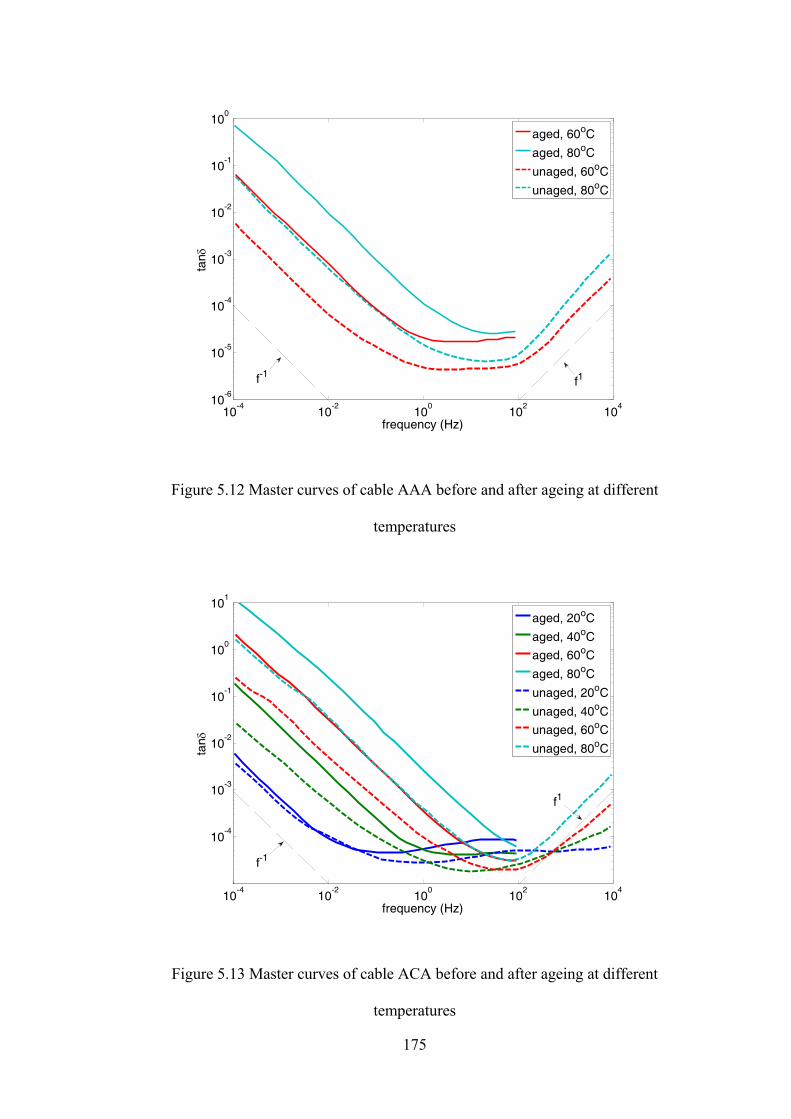
175
10-4
10-2
100
102
10410
-6
10-5
10-4
10-3
10-2
10-1
100
frequency (Hz)
tan δ
aged, 60oC
aged, 80oC
unaged, 60oC
unaged, 80oC
f-1 f1
Figure 5.12 Master curves of cable AAA before and after ageing at different
temperatures
10-4
10-2
100
102
104
10-4
10-3
10-2
10-1
100
101
frequency (Hz)
tan δ
aged, 20oC
aged, 40oC
aged, 60oC
aged, 80oC
unaged, 20oC
unaged, 40oC
unaged, 60oC
unaged, 80oC
f1
f-1
Figure 5.13 Master curves of cable ACA before and after ageing at different
temperatures

176
Comparisons can be made with the master curves of unaged model cables. Figure 5.12
shows the comparison for cable AAA at the temperatures of 60°C and 80°C. For cable
ACA, the comparison is shown in Figure 5.13. It can be seen that for both homo- and
co- polymer cables, the loss tangent has about 10 times increase for all the temperatures,
while the shapes of the loss spectra keep the same.
5.4 Ageing effects on conductivity of model power cables
5.4.1 Influence of thermal ageing on conductivity of model power cables
The conductivity of the aged model power cables has been measured with the 1kV
battery voltage supply and Keithley 617 electrometer. The measurement setup and
conditions were the same as for the unaged cables. The thermally aged cable samples,
AAA, ABA and ACA, were tested after four hours charging time under four
temperatures: 20°C, 40°C, 60°C and 80°C. The DC conduction currents for the aged
cable AAA, in comparison with the unaged cable, are shown in Figure 5.14. The DC
conduction current increases at higher temperatures. In the temperature range from
20°C to 80°C, the DC conduction current is from 2.57×10⁻¹³A to 5.13×10⁻¹⁰A. A linear
increasing trend can be seen in the semi-log scale. The trend is parallel to that of the
unaged cable AAA, for which the current at 20°C is absent in the plot because of
measurement limitations. The measurement results suggest the aged homo-polymer
cable AAA still has an increasing conductivity at higher temperatures. It becomes more
conductive after thermal ageing, e.g. the DC conduction current at 80°C is 16 times
bigger than that of unaged cable sample, 3.25×10⁻¹¹A. Thermal ageing, therefore, has a
significant effect on DC conductivity.
177
20 30 40 50 60 70 8010
-13
10-12
10-11
10-10
10-9
temperature (oC)
curr
ent (
A)
agedunaged
Figure 5.14 DC conduction current of aged and unaged cable AAA at different
temperatures
Applying the same equation (introduced in chapter 3),
LUIrr i
πσ
2)/ln( 0= Equation 5-2
the conductivity of the aged model cables can be calculated. The calculation results are
plotted in Figure 5.15. The conductivity of aged cables is interconnected with solid lines,
while the results of unaged cables have dashed lines. It can be seen that the conductivity
for all aged cables have increasing temperature dependence. In the semi-log scale graph,
the conductivity of cable AAA has a linear relationship with the absolute temperature,
indicating a relation of T∝σlog . Cable ABA has bigger conductivity than cable AAA.
It has the same linear increasing trend until 60°C, but deviation was measured with
bigger increment at 80°C. Among the three cables, the co-polymer cable ACA has the
biggest conductivity. Its temperature dependence is curved with relatively smaller

178
increment at higher temperatures, which is different from the homo-polymer cable AAA
and ABA. Compared with the unaged cables, the conductivity for all the model cables
becomes bigger. The cables still have the same sequence as unaged cables, with cable
AAA having the smallest conductivity. With the same thermal ageing condition, it is
found that cable ABA has the biggest conductivity increment. Although co-polymer
cable ACA has the biggest absolute conductivity, the increment after ageing process is
smaller than those of the two homo-polymer cables.
20 30 40 50 60 70 8010
-18
10-17
10-16
10-15
10-14
10-13
10-12
Temperature (oC)
σ (S
/m)
AAA, agedAAA, degassedABA, agedABA, degassedACA, agedACA, degassed
Figure 5.15 Conductivity of aged model power cables, compared with unaged cables
5.4.2 Activation energy change after thermal ageing
The thermal activation energy of the model power cables can be studied through the
measurement results of conductivity at different temperatures. According to Arrhenius
equation

179
kTEa
e−
×= 0σσ Equation 5-3
which can also be written as
kTEa−= 0lnln σσ
Equation 5-4
the logarithmic conductivity should have linear relationship with the reciprocal of
temperature
T1ln ∝σ Equation 5-5
The thermal activation energy aE can be obtained from the gradient of the straight line.
In the Arrhenius equation, the value of the "y-intercept" corresponds to a pre-
exponential factor 0lnσ . k is the Boltzmann’s constant that is 1.38×10⁻²³ J/K or
8.617×10⁻⁵ eV/K.
The Arrhenius plots for different aged model power cables are shown in Figure 5.16.
Linear fitting lines are also plotted for the calculation of thermal activation energy. The
linear relationship of the fitting lines and the activation energies calculated from the
gradients are in separate boxes with relevant colours. From the measurement results, it
can be seen that aged cables AAA and ACA have good fitting. The measurement results
are closely scattered around the fitted lines. It can also be seen that the results of AAA
have opposite curvature to that of ACA. This suggests that the homo-polymer cables
have bigger thermal activation energy at higher temperatures and the co-polymer cables
have decreasing activation energy at higher temperatures. For cable ABA, the fitting is

180
very good at the temperatures except 80°C; while at higher temperatures above 60°C,
the increasing conductivity has a bigger gradient which suggests higher activation
energy. The activation energy values for all three cables are very close – 1.13eV for
cable AAA and 1.23 for cable ACA.
2.8 2.9 3 3.1 3.2 3.3 3.4 3.5x 10
-3
-42
-40
-38
-36
-34
-32
-30
-28
1/T (K-1)
lnσ
AAA, aged, Ea=1.13eVABA, aged, Ea=1.21eVACA, aged, Ea=1.23eVAAA, unaged, Ea=1.08eVABA, unaged, Ea=1.10eVACA, unaged, Ea=1.17eV
All types of the model power cables haveincreased activation energy after thermal ageing
Figure 5.16 Arrhenius plot for aged cables with linear fittings, thermal activation
energies calculated from the gradients of the linear fitting lines
The effects of ageing can be studied by the calculated thermal activation energy in
Figure 5.16. The most noticeable ageing effect is that the activation energy for all cables
has increased, e.g. cable ABA has the biggest increment from 1.10eV to 1.23eV. There
is a small increment of activation energy but found for both homo-polymer and co-
polymer cables. This increment of thermal activation energy can be characteristic for
the ageing evaluation of power cables. Compared with cables having different
insulation materials, homo-polymer cables have lower activation energy than the co-
polymer cables before and after the ageing. After the ageing process, the co-polymer

181
cable ACA still has the biggest activation energy. Similar experiments of the same kind
on XLPE material [143] can be compared with the results in this study. The activation
energy was found to be 0.89eV for unaged XLPE and 1.06eV for aged sample.
5.5 Dielectric loss measurement using Schering bridge
5.5.1 Measurement system and sample preparation
In order to study the ageing effects with higher electric fields at mains frequency and
field dependence of the dielectric response of the model power cables, a Schering
bridge was used. The experiment was carried out using the Schering bridge at Areva
T&D. The measurement system is shown in Figure 5.17. The high voltage part inside an
interlocked safety cage is in the left photo. A sample oven, a potential divider and a
100pF standard high voltage capacitor (the Bushing Company Ltd, UK) are included in
the high voltage cage. The low voltage control part is in the right photo that contains the
control panel of the Schering bridge (Hartmann & Braun, Western Germany), null
detector (Tettex Instrument, Switzerland), control panel for the potential divider and
power transformer controller for high voltage delivery.
Figure 5.17 Schering bridge system setup. High voltage part in the left photo and low
voltage control part in the right photo.

182
Before measuring the cable samples, an auxiliary bridge was balanced to exclude the
influence of stray capacitance. Measurements were taken at 20°C for aged and unaged
cables. The applied voltages were from 1.5kV to 22.5kV. Cables ABA and ACA were
also tested at different temperatures up to 80°C. During the measurement, the loss
tangent value can be read directly from the Schering bridge adjusting panel.
Capacitance of the cable samples XC can be calculated from
3
4
RRCC N
X⋅
= Equation 5-6
where NC is 100pF standard high voltage capacitor; 3R and 4R correspond to the
resistance in the other arms of the Schering bridge. For measuring currents less than
80mA in this study, Ω=π
10004R and 3R can be measured together with loss tangent.
Figure 5.18 Cable sample termination preparation on one end (symmetric for the other)
Terminals of the cable samples were specially prepared to prevent leakage current and
flashover under the high electric field. The diagram for preparing the cable terminals is
shown in Figure 5.18. There is a 6cm distance without outer semicon layer between the
conductor and the guard electrode. At the triple junction of the insulation, guard
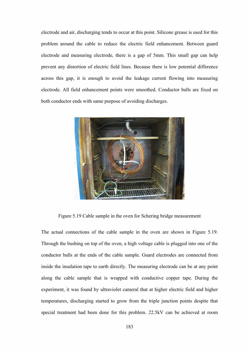
183
electrode and air, discharging tends to occur at this point. Silicone grease is used for this
problem around the cable to reduce the electric field enhancement. Between guard
electrode and measuring electrode, there is a gap of 5mm. This small gap can help
prevent any distortion of electric field lines. Because there is low potential difference
across this gap, it is enough to avoid the leakage current flowing into measuring
electrode. All field enhancement points were smoothed. Conductor balls are fixed on
both conductor ends with same purpose of avoiding discharges.
Figure 5.19 Cable sample in the oven for Schering bridge measurement
The actual connections of the cable sample in the oven are shown in Figure 5.19.
Through the bushing on top of the oven, a high voltage cable is plugged into one of the
conductor balls at the ends of the cable sample. Guard electrodes are connected from
inside the insulation tape to earth directly. The measuring electrode can be at any point
along the cable sample that is wrapped with conductive copper tape. During the
experiment, it was found by ultraviolet cameral that at higher electric field and higher
temperatures, discharging started to grow from the triple junction points despite that
special treatment had been done for this problem. 22.5kV can be achieved at room

184
temperature without discharges, but discharging started above 15kV at high
temperatures from 40°C. Therefore, the maximum applied field was determined as
15kV for higher temperatures. The maximum applied electric field is also restricted by
the radius of the model cables.
5.5.2 Measurement results
Figure 5.20 shows the loss tangent measurement results on different aged and unaged
model power cables at room temperature: 20°C. It can be seen that the loss tangent
increased after ageing, e.g. the loss tangent of cable AAA under 15kV increased from
7.11×10⁻⁴ to 1.08×10⁻³. Comparing different cables, homo-polymer cable AAA has the
lowest loss tangent while co-polymer cable ACA has highest loss for both aged and
unaged samples.
0 5 10 15 20 2510
-4
10-3
Voltage (kV)
tan δ
AAA, agedABA, agedACA, agedAAA, degassedABA, degassedACA, degassed
Figure 5.20 Loss tangent of aged and unaged cable samples at 20°C

185
Figure 5.21 Field dependence of loss tangent for different 12kV power cables [145]
0 5 10 15 20 2510
-4
10-3
Voltage (kV)
tan δ
20oC, aged
40oC, aged
60oC, aged
80oC, aged
20oC, degassed
40oC, degassed
60oC, degassed
80oC, degassed
Figure 5.22 Loss tangent of aged and unaged homo-polymer cable ABA at different
temperatures
There is a general law of electric field dependent conductivity with exponential increase
in higher field range [144]. For all types of model power cables in this study, the
electric field dependence in this field range does not vary a lot. This stable electric field
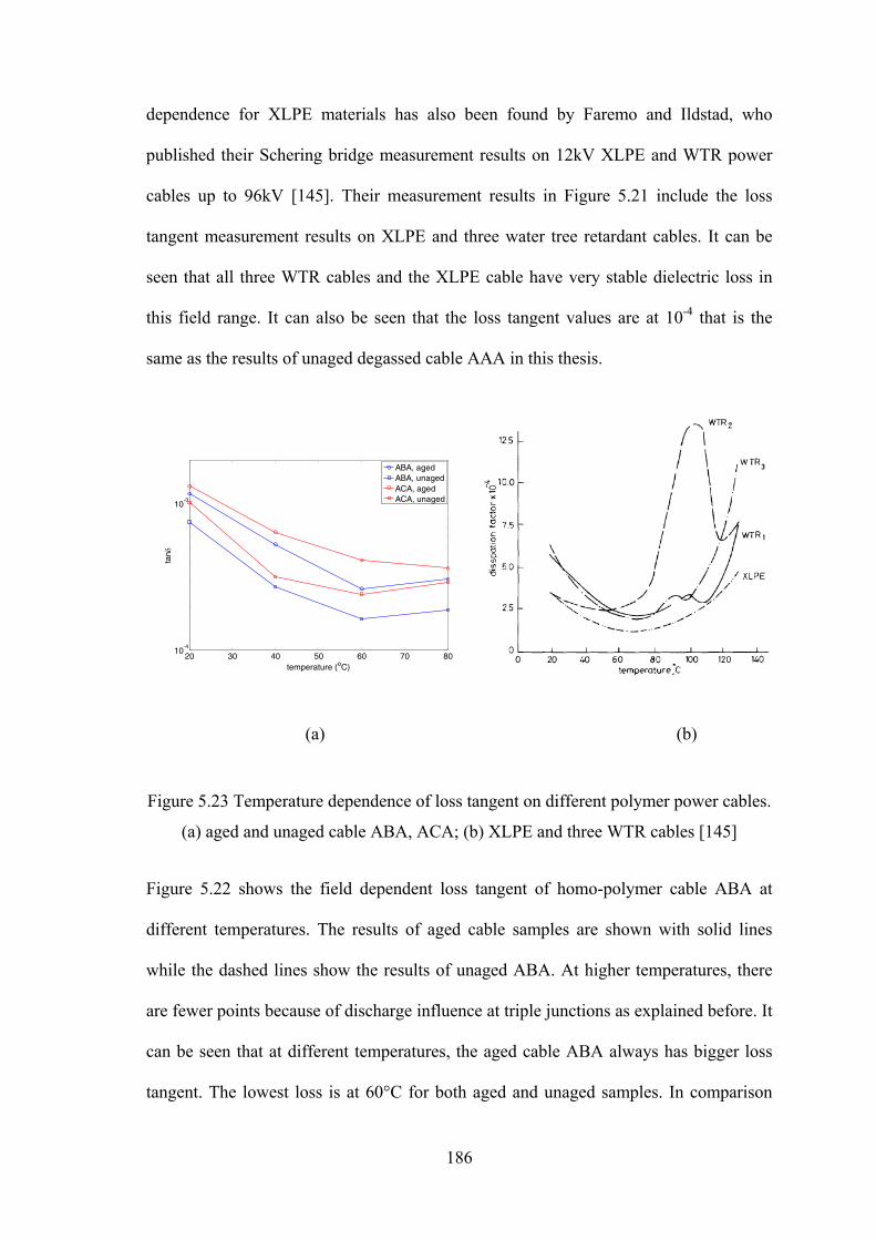
186
dependence for XLPE materials has also been found by Faremo and Ildstad, who
published their Schering bridge measurement results on 12kV XLPE and WTR power
cables up to 96kV [145]. Their measurement results in Figure 5.21 include the loss
tangent measurement results on XLPE and three water tree retardant cables. It can be
seen that all three WTR cables and the XLPE cable have very stable dielectric loss in
this field range. It can also be seen that the loss tangent values are at 10-4 that is the
same as the results of unaged degassed cable AAA in this thesis.
20 30 40 50 60 70 8010
-4
10-3
temperature (oC)
tan δ
ABA, agedABA, unagedACA, agedACA, unaged
(a) (b)
Figure 5.23 Temperature dependence of loss tangent on different polymer power cables.
(a) aged and unaged cable ABA, ACA; (b) XLPE and three WTR cables [145]
Figure 5.22 shows the field dependent loss tangent of homo-polymer cable ABA at
different temperatures. The results of aged cable samples are shown with solid lines
while the dashed lines show the results of unaged ABA. At higher temperatures, there
are fewer points because of discharge influence at triple junctions as explained before. It
can be seen that at different temperatures, the aged cable ABA always has bigger loss
tangent. The lowest loss is at 60°C for both aged and unaged samples. In comparison

187
with the experimental results by Faremo and Ildstad, the same temperature dependence
can be found in Figure 5.23. For the 12kV XLPE cables in (b), it has a decreasing loss
tangent from 20°C to 60°C. After this lowest point, the loss tangent increases again
towards higher temperatures. WTR-XLPE cables also have this temperature dependence.
The results in (a) have the same temperature dependence for cable ABA and ACA, both
aged and unaged. Homo-polymer cable ABA has the closest trend as in (b). The bigger
magnitudes in this study may be due to the different XLPE materials, thickness of the
insulation, additives and crystallinity.
(a) (b)
Figure 5.24 Field dependent ageing effect of XLPE power cables at 0.1Hz. (a)
increasing loss tangent for aged cable A1 and B1, in comparison with less aged cable
C1 and D1 [146]; (b) Ageing effect with higher applied voltages on new and aged 15kV
XLPE cable [147]
Another noticeable ageing effect for homo-polymer cable ABA (Figure 5.22) is that the
field dependence becomes bigger. For example at 60°C, the loss tangent increases from
188
1.58×10⁻⁴ under 1.5kV to 1.85×10⁻⁴ under 22.5kV for unaged cable, while it increases
from 2.48×10⁻⁴ under 1.5kV to 3.53×10⁻⁴ under 22.5kV for aged cable. As shown in
Figure 5.23 (a), this ageing effects have also been found by Sverre Hvidsten, Erling
Ildstad, Bjorn Holmgren and Peter Werelius [146] and cable testing company [147].
Their study at lower frequency of 0.1Hz has the same results that increasing loss tangent
was measured with increasing electric field for aged XLPE cables while the loss was
unchanged for unaged cables. The same field dependence ageing effects are found in
this thesis at high frequency of 50Hz. This suggests that this ageing effect is always
present regardless of frequency.
5.6 Conclusions
Thermal ageing effects have been experimentally studied on the model power cables:
1. The dielectric loss spectra have increased magnitudes after the accelerated
thermal ageing process.
2. Thermal ageing can increase the dielectric loss and conductivity of both homo-
polymer and co-polymer power cables. Oxidation may create extra polar groups
in the insulation.
3. Schering bridge tests indicates that the electric field has bigger influence on the
thermally aged cables than new cables

189
6 Thermal breakdown simulation on model power cables
6.1 Introduction
The breakdown of dielectrics is closely related to the thermal instability under electric
field. This problem has been studied for a long time with a large amount of literature,
e.g. Whitehead has investigated this type of breakdown in great detail in his dedicated
works [148]. With the realization of its importance, the thermal breakdown for DC
power cables has been intensively studied by Fallou and Eoll [149] [150]. Experimental
evidence on polyethylene and oil impregnated paper cables has shown a reduction in
breakdown strength with temperature difference across the insulation [150] [151]. Their
theoretical study for thermal breakdown has suggested some mathematical methods for
the estimation of maximum electric field based on the nonlinear conductivity of the
cable insulation. Analytical methods for the computation of temperature-related
breakdown in both thick and thin specimens with parallel plane electrodes have already
been covered by Dissado, Fothergill and O’Dwyer [152] [12].
As far as high voltage power cables are concerned, the complexity of thermal
breakdown study comes not only from the heat transfer due to its special geometry but
also due to multifactor conductivity that is dependent on both temperature and electric
field. This thermo-electric breakdown in cable insulation is a consequence of the
temperature rise in the insulation mainly due to the Ohmic losses in the conductor and
to the dielectric loss in the cable insulation. The latter component is due to conduction
loss for DC application and also includes polarization loss for AC cables. It is a strong
function of the applied field and temperature. If the heat generated by the energy loss

190
cannot be dissipated efficiently, it will give rise to the heating of the insulation and
eventual thermal breakdown. Any microscopic differential volume element inside the
insulation can initiate this thermal breakdown process. The heat dissipation across the
cable’s outer boundary is directly dependent on the thermal conductivity of the
insulation material and the boundary conditions of the surrounding environment. For
one dimensional consideration on power cables, the high voltage electrode is practically
thermally insulated. Any differential element in the bulk insulation close to this
electrode only allows heat flow into the element and not out of it. Therefore, the thermal
breakdown is greatly related to the boundary conditions, which are usually impossible
to compute exact solutions for complex boundary geometries. There exists a steady state
thermal breakdown voltage or maximum thermal voltage for every unique power cable.
No thermal breakdown should take place below this voltage. In a real application, the
time to reach this thermo-electric equilibrium in HVDC cables depends on the thermal
and electrical time constants of the cable insulation which are typically less than 24
hours [153]. The time to breakdown can be much less than 24 hours for voltages much
greater than the maximum thermal voltage. A small incremental voltage above the
maximum thermal voltage could result in a runaway in a very short time due to a
positive thermal feedback effect that is basically caused by the temperature and field
dependent electrical conductivity [154] [155]. The mathematical complexity for the
multifactor conductivity precludes an analytical solution of thermal breakdown study on
power cables.
The estimated theoretical calculation of maximum thermal voltage for thermal
breakdown phenomenon has been suggested in the literature mentioned above. However,
the distributions of the critical parameters such as electric field and temperature had not
been easily obtained until the computer aided programs emerged in recent years. In this
191
chapter, the thermal breakdown simulation with finite element method is studied. Based
on the partial differential equations for this multi-physics phenomenon, the thermal-
electrical behaviour of the model power cables under DC field can be simulated. The
experimental results in previous chapters are used to determine the parameters. The
distributions of different parameters can be visualized in FEMLab program.
6.2 Mathematical model of thermal‐electric behaviour for power cables
The mathematical prototype for the thermal-electric behaviour is based on the partial
differential equation (PDE) for heat transfer
QTktTCP =∇•∇−∂∂ )(ρ Equation 6-1
where ρ is density of the thermally conductive material; HC is heat capacity; k is
thermal conductivity and Q is heat source [156]. In this equation, temperature T is the
variable. The first term on the left side represents the time dependence and the second
term represents spatial distribution. In this study, the heat source Q is from resistive
heating
2),( EETJEQ σ== Equation 6-2
where J is current density; σ is conductivity; E is electric field. The conductivity
may be either DC conductivity with DC electric field or AC conductivity at 50Hz
frequency of the alternating electric field.
Combining Equation 6-1 and Equation 6-2, the PDE of thermal continuity under steady
state for a one-dimensional heat flow is

192
0)())((2
=⎟⎠⎞
⎜⎝⎛+
dzzdU
dzzdTk
dzd σ Equation 6-3
where )(zU is electrical potential function in z coordinate as shown in Figure 6.1 (a).
(a) parallel geometry
(b) cylindrical geometry
Figure 6.1 Sectional views of one dimensional heat flow

193
For cylindrical geometry as for cables (Figure 6.1 (b)), the steady state PDE changes to
0)())((1 2
=⎟⎠⎞
⎜⎝⎛+
drrdU
drrdTrk
drd
rσ Equation 6-4
where r is radial distance from the origin; )(rT and )(rU are temperature and
potential at the radial position r [153]. In both Equation 6-3 and Equation 6-4, the first
term in the above equation represents the divergence of heat and the second term is the
amount of heat generated in a differential volume element in insulation due to the
dielectric loss.
For a power cable under operation, the heat flow model can be built as in Figure 6.2. In
the inner conductor, the energy loss in form of heat is due to Joule heating of the load
current and it is injected into the insulation layer that is the only way of dissipating the
heat. Together with the dielectric loss inside the insulation layer, the heat due to the
conductor loss flows through the insulation and all the energy loss is dissipated into the
ambient environment. The highest temperature occurs at the conductor-insulation
boundary. As a very big heat capacitor, the environment has a constant temperature in
this model. This may be a reasonable assumption for a sub-sea cable which has the
ambient temperature of approximately 4˚C. Other solutions would be possible e.g. the
cable was buried in a trench. In order to solve the PDE, boundary conditions are needed.
There are some assumptions for the boundary conditions and environment domain:
1. the inner conductor injects heat, due to load current joule heating of over a unit
length of cable IL2Rcon, into bulk insulation; the inner boundary of the insulation
cannot dissipate heat into the conductor.

194
2. the heat only dissipates from the outer boundary of the insulation.
3. the medium outside the insulation has constant temperature (infinite thermal
conductivity)
Figure 6.2 Heat flow of a DC power cable
These assumptions for the cable’s heat flow model can be mathematically translated as:
1. At the inner conductor-insulation boundary,
conLrr RIdr
rdTkr 21
1
)(2 −=+=π Equation 6-5
where LI is the load current; conR is the conductor resistance per unit length.

195
2. At insulation outer boundary,
UIRIdr
rdTkr conLrr −−=−=2
22
)(2π Equation 6-6
where UI represents the power of all the dielectric loss in the cable insulation.
3. Outside the insulation,
aTrT =)( 2 Equation 6-7
With the above assumptions of boundary conditions, Equation 6-4 for cable geometry
can be transformed with rewriting and integration as
∫∫ +=−2
1
2
1
122
2)(
)(
2 r
r
conLrT
rT
drr
RIdTkUσπσ
Equation 6-8
With the upper bound on maximum insulation temperature Tmax, the maximum thermal
voltage of a loaded cable Umc can be calculated as
∫∫ −=2
1
max 12 22
r
r
conLT
Tmc dr
rRIdTkU
aσπσ
Equation 6-9
This is the general expression of the solution. The first term in the right hand side
determines the maximum thermal voltage without heat injection from conductor, while
the second term is due to external heat, which reduces the maximum thermal voltage.
The integration on the right side of Equation 6-9 is a function of conductivity, which is
field and temperature dependent. There is no general theoretical model for the electrical
conductivity applicable to all kinds of solid dielectrics. There are some semi-empirical

196
formulations all of which appear formally similar. A commonly used expression as
applied to cable insulation is
)(TbEa
Ae−
=σ Equation 6-10
where A is material specific constant with unit of S/m; a is known as the stress
coefficient; b is Boltzmann constant [157] [158]. It has been shown to be applicable
over a wide range of temperature and electric field for many types of dielectrics
including XLPE. This may be compared with another suggested equation with similar
expression and a physical basis of field assisted hopping conduction [154] [155]
EEB
eA Tb )sinh()(⋅′=
−σ Equation 6-11
where A′ is just a coefficient with unit of V/Ωm2 and B is the other coefficient for
electric field dependence with unit of m/V. Practically EB is a large positive value.
Therefore when the hyperbolic function term is written with exponential function form,
the approximation of Equation 6-11 will be the same as Equation 6-10
( )
)(
)(
)(
)(
2
21
)sinh(
TbEB
EBTb
EBEBTb
Tb
Ae
eeE
A
eeE
eA
EEB
eA
−
−
−−
−
=
⋅′
≈
⎥⎥⎦
⎤
⎢⎢⎣
⎡−⋅′=
⋅′=σ
Equation 6-12
The simpler Equation 6-10 is a more widely used empirical function of conductivity
over a range of several decades. Therefore, Equation 6-10 is used in this study. Because

197
the conductivity is dependent on electric field, which is dependent on the radius r, the
heat source term for one-dimensional case in the continuity equation becomes very
complex to solve
222 )())(),(()())(),(()(⎟⎠⎞
⎜⎝⎛⋅=⎟
⎠⎞
⎜⎝⎛⋅=⎟
⎠⎞
⎜⎝⎛
drrdU
drrdUrT
drrdUrErT
drrdU σσσ Equation 6-13
To overcome this difficulty, mean value theorems can be used to simplify the field
dependent electrical conductivity which is an averaged value of field for the whole
insulation [153] [159]
))(()),(()),(())(),(( 00 rTErTdUrTrErT σσησησσ === Equation 6-14
where η is an empirical constant to adjust the averaged electric field 0E and produce a
conductivity that is dependent on temperature and applied voltage. A more conservative
assumption is applied in this study with the highest conductivity value at the inner
boundary
))(),(())(),((1rrdr
rdUrTrErT == σσ Equation 6-15
With the basic mathematical model, relevant equations and parameters, the simulation
can thus be done numerically. The distributions of electric field and temperature in both
transient and steady state are simulated with FEMLAB, which is an interactive
environment for modelling and solving scientific and engineering problems based on
partial differential equations. When solving the PDEs, FEMLAB uses the proven finite

198
element method (FEM) that has a prominent position among the most famous three
methods – finite element method (FEM), finite volume methods (FVM) and finite
difference methods (FDM) [160].
6.3 Thermal breakdown simulation setup in FEMLAB
Thermal breakdown occurs when thermal equilibrium cannot be achieved. Figure 6.3
shows the thermal breakdown process when the applied voltage exceeds the maximum
thermal voltage (MTV) at the hottest point inside the cable insulation. If the voltage is
less than MTV, thermal equilibrium can be reached after some settling time. If the
voltage equals MTV, the power cable can operate stably under the highest electric field.
When the voltage is higher than MTV, the heat due to dielectric loss and conductor loss
cannot be efficiently dissipated and thermal breakdown will occur. Therefore, in the
simulation, MTV is the most concerned parameter to find out.
Figure 6.3 Time dependent thermal breakdown process at the maximum temperature
with relationship to maximum thermal voltage

199
Based on the measurement results in previous chapters, the model power cables can be
simulated using Equation 6-10 to determine the field and temperature dependent
conductivity. The field dependent conductivity exponentially fitted from Schering
bridge measurement results is shown in Figure 6.4 (a) and it is extrapolated to
500kV/mm mean field in Figure 6.4 (b).
a=0.0077
a=0.0082
a=0.0142
5 10 15 20 25 30 35 40 45 5010
-12
10-11
10-10
electric field (kV/mm)
cond
uctiv
ity (
S/m
)
cable AAA at 20oC
cable ABA at 20oC
cable ACA at 20oC
(a) exponential fitting of conductivity from experiment results
50 100 150 200 250 300 350 400 450 50010
-12
10-11
10-10
10-9
10-8
electric field (kV/mm)
cond
uctiv
ity (
S/m
)
cable AAA at 20oC
cable ABA at 20oC
cable ACA at 20oC
a=0.0077
a=0.0082
a=0.0142
(b) extrapolation of conductivity to higher electric field
Figure 6.4 Field dependence of model power cables, fitted from experimental data

200
Figure 6.5 Electric field distribution in the model cable insulation with 150kV
When 150kV is applied on 1.5mm insulation, the electric field distribution is shown on
Figure 6.5. The average electric field should be 100kV/mm, but the distribution for
cable geometry has the highest field near the conductor core with 140kV/mm. The
lowest electric field is 70kV/mm near the outside. This electric field distribution at a
constant temperature can also be found in literature with [162]
i
o
rrr
UEln
1=
Equation 6-16
where E is the electric field, U is the applied voltage, r is the radius from the cable
geometry centre, or and ir are the outer and inner radius of the cable insulation layer.
Because the maximum field is 1.4 times as the averaged mean field, a multiplying factor
of 1.4 is used in this study to conservatively simplify the field dependence in Equation
201
6-16. It should be noticed that this electric field distribution is different in practice with
varying temperature distribution and may be even reversed in certain situations.
With the thermal activation energy aE , the temperature dependence can be integrated
into the final expression. For the homo-polymer cable AAA ( eVEa 08.1= ), the
expression for conductivity is
TU
Tb
dUa
ee
AeTU12533
5.14.10082.0
6
)4.1(
10168.15
),(−
×
−
×××=
=σ Equation 6-17
Here, U should have the unit of kV and d should have the unit of mm, because E is in
the unit of kV/mm. σ is S/m and T is in Kelvin. This is used throughout the following.
Similarly, the conductivity for homo-polymer cable ABA ( eVEa 10.1= ) is
TU
eeTU12765
5.14.10142.0
610816.36),(−
×
×××=σ Equation 6-18
and for co-polymer cable ACA ( eVEa 17.1= ) is
TU
eeTU13578
5.14.10077.0
610213.877),(−
×
×××=σ Equation 6-19
A symmetric 2D model is used with 2528 mesh points in FEMLAB, as shown in Figure
6.6. This model represents the cross section along a radius through the insulation (see
Figure 6.2). The horizontal direction is the radial thickness, while the vertical axis is the
axial direction of the cable with both end thermally and electrically insulated so that the
electrical current and heat can only flow through the insulation in radial direction. This
is really a 1-D model, so only changes in the radial direction are expected. This

202
Multiphysics modelling requires boundary definition and sub-domain definition for both
electrical heating process and thermal conduction process.
Figure 6.6 The geometry of axial symmetry 2D definition for the model power cables,
with 2528 mesh points in the area of 1.5mm×10mm
The modelling parameters for electrical heating are
• Boundary 1: electrical potential/applied voltage;
• Boundary 2: electrical insulation;
• Boundary 3: electrical insulation;
• Boundary 4: ground;

203
• Sub-domain:
conductivity expression for model power cable: ),( TUσ
initial value: 0)( 0 =tU
The modelling parameters for thermal conduction are
• Boundary 1: thermal insulation without heat flux or heat flux due to conductor
loss; the simulation without conductor loss is firstly carried out; when there is
heat flux crossing boundary 1, it can be calculated with
where I is load current; mΩ×= −81072.1ρ is the resistivity of copper; r is the
radius of the conductor core.
• Boundary 2: thermal insulation;
• Boundary 3: thermal insulation;
• Boundary 4: ambient temperature 0T ;
• Sub-domain:
Thermal conductivity: 0.45 W/mK
32
222
2
222fluxheat
rI
rLrLI
rLRLITk
πρ
ππ
ρ
π===∇= Equation 6-20

204
Density: 1100 kg/m3
Specific heat capacity: 2000 J/kg
Heat source: )(),( 2 rETUQ σ=
Initial value: 00 )( TtT = , the insulation sub-domain has the same
temperature as ambient.
Figure 6.7 Temperature distribution when thermal breakdown occurs, with the highest
temperature of 421K in the breakdown channel
Thermal breakdown voltage can be found when the mathematical solution in FEMLAB
is not convergent. If the applied voltage exceeds the MTV in a specific situation, the
software cannot solve the PDE, and it will give out error message with parameter

205
distributions after thermal breakdown, as shown in Figure 6.7. Horizontal axis is the
thickness of insulation layer from 1.4mm to 2.9mm; vertical axis is 10cm length of
cable for this simulation study. All the following simulation results have the same
geometry. It can be seen that when the initial temperature is 298K (20°C), the highest
temperature after breakdown inside the breakdown channel can be 420K (127°C) that
will totally damage the insulation material.
6.4 Simulation results of model power cables
6.4.1 MTV without load current at different ambient temperatures
The MTV for the model power cables at different temperatures are plotted in Figure 6.8.
The temperature ranges from 293K (20°C) to 343K (70°C). Higher temperatures were
not simulated because XLPE starts to melt from 353K (80°C). It can be seen that the
MTV decreases when temperature increases for all three cables. With homo-polymer
insulation, cable AAA at 293K has the highest MTV of 340kV, which is 226kV/mm
with its 1.5mm insulation. When the temperature increases to 343K, its MTV drops to
52kV (35kV/mm). At lower temperatures, homo-polymer cable ABA has lower MTV
than co-polymer cable ACA. This may be due to the higher conductivity that makes
electric field distribution smoother and, therefore, slows down the temperature increase.
Similar simulation on the thermal breakdown of HVDC cables has been done by Ch.
Chakradhar Reddy and T. S. Ramu [153]. With bigger conductor radius of 22mm and
insulation thickness of 22mm, the maximum breakdown voltage (MTV) calculation
results are plotted in Figure 6.9 (a). Using MATLAB estimated calculation on MTV, it
has a linear decrease at higher temperatures. The breakdown electric field is about
55kV/mm with 1000A load current as heat injection source through the inner boundary.

206
Another recently published paper [161] has simulated the thermal breakdown of MgO
filled XLPE cables. Higher breakdown field was found for different filler contents, as
shown in Figure 6.9 (b).
290 300 310 320 330 3400
50
100
150
200
250
300
350
temperature (K)
max
imum
ther
mal
vol
tage
(kV
)
AAA, theoretical MTVAAA, practical MTVABA, theoretical MTVABA, practical MTVACA, theoretical MTVACA, practical MTV
Figure 6.8 MTV for degassed homo-polymer and co-polymer model power cables
(a) (b)
Figure 6.9 MTV simulation results by (a) Chakradhar Reddy [153] and (b) T. S. Ramu
[161]

207
Practical consideration on the melting temperature of XLPE material was included
during the simulation process. After reaching steady state, there is a temperature
increase inside the cable insulation. The hottest point is the boundary to central
conductor. If the maximum temperature of this boundary reaches 353K, melting of
XLPE insulation will start, and breakdown will occur from this position. In this
simulation, the original temperature everywhere in the cable insulation is assumed to be
the same as ambient temperature.
290 300 310 320 330 340 350310
320
330
340
350
360
370
380
353
original temperature (K)
max
imum
tem
pera
ture
in s
tabl
e st
ate
(K)
AAAABAACA
melting temperatureof cable insulation
Figure 6.10 Maximum temperature at the inner boundary under MTV
The maximum temperature can be calculated in FEMLAB, as shown in Figure 6.10. It
can be seen that the maximum temperature in stable state exceeds 353K when the
original temperature is above 323K (50°C). Therefore, the MTV should be recalculated
to ensure that the maximum temperature does not exceed 353K. The recalculated

208
practical MTV are also plotted in Figure 6.8 in comparison with theoretical MTV. There
is certain amount of MTV decrease after restricting the maximum temperature, e.g. the
MTV of cable AAA with 343K ambient drops from 52kV to 44kV.
Figure 6.11 Temperature and heat flux distribution in the insulation of cable AAA in
FEMLAB, at 70kV under stable state (t=105s)
Because of the cylindrical cable geometry, the temperature in the cable insulation does
not have a uniform distribution. Its stable state distribution is dependent on the
dimensions of the cable, load current value, ambient temperature and applied voltage.
Figure 6.11 shows the FEMLAB simulation results of temperature distribution with heat
flux (white arrows). Blue colour area represents the lower temperature and red area for
higher temperature, as shown in the colour bar on the right side of the graphs. The
radius along the insulation increases from left to right. After reaching stable state at
70kV, it can be seen that the highest temperature is at inner boundary and gradually
decreases along the radial thickness of the cable insulation. There is very little

209
difference for the temperature distribution for voltages except at MTV, which can cause
big temperature variation but still keep the same distribution trend. Heat flux becomes
bigger near the outer boundary because more accumulated heat due to dielectric loss is
dissipated to the environment.
0 0.5 1 1.5x 10
-3
290
295
300
305
310
315
320
radial distance from conductor-insulation boundary (m)
tem
pera
ture
(K
)
70kV120kV170kV220kV260kV300kV340kV, MTV
Figure 6.12 Temperature distribution in cable insulation under different voltages, when
ambient temperature is 293K
The temperature distribution in the radial direction can be compared for different
voltages. Figure 6.12 shows the temperature distribution in stable state inside the cable
insulation. The original temperature for cable AAA is 293K. All curves are plotted after
the cable insulation reaches stable state. When the applied voltage is much lower than
MTV, there is very little increase of 0.037K. Higher voltage increases the stable state
temperature inside the insulation, e.g. 2.7K is the increase at the inner boundary when
the voltage is 260kV. Under MTV of 340kV, the maximum temperature is 320.4K with
27.4K increase on the original ambient temperature 293K. The comparison of

210
temperature distribution under different voltages indicates that an increase of voltage
that is much lower than MTV does not induce big temperature gradient from the inner
boundary to the outer boundary. The maximum temperature is well below 295K with
100kV increase from 70kV to 170kV. However, the maximum temperature increases
much faster from 260kV to 340kV. 40kV increase from 300kV to 340kV increases the
maximum temperature from 299K to 320.4K. This implies that it will be dangerous for
power cables to operate even under the voltages of 100kV below its MTV.
Like the temperature distribution, the electric field distribution is also voltage dependent.
The FEMLAB simulation results of electric field distribution for cable AAA with
ambient temperature 293K is shown in Figure 6.13. Graph (a) shows the field
distribution under 340kV and graph (b) under 70kV. The distribution under a higher
voltage in (a) has the maximum electric field at outer boundary. Compared with graph
(a), graph (b) has opposite distribution with maximum field at inner boundary. Graph (b)
under lower voltage of 70kV in stable state has a similar electric field distribution to
that of the original distribution, with the highest field at the inner boundary due to the
cylindrical cable geometry. The maximum field at the inner boundary is 68.52kV/mm,
about twice of that at the outer boundary, 33.25kV/mm, while the mean field is
46.67kV/mm. Graph (a) under MTV with a reverse field distribution has increasing
magnitudes from inner boundary to outer boundary. The maximum field at the outer
boundary is 1442kV/mm, about twice of that at the inner boundary, 73.88kV/mm. With
practical consideration of the intrinsic electrical breakdown strength of 800kV/mm, the
insulation material near the outer boundary will breakdown due to electric field
enhancement. Therefore the actual breakdown should be lower than this maximum
thermal voltage.

211
(a) 340kV, MTV
(b) 70kV
Figure 6.13 Electric field distribution in the insulation of cable AAA in FEMLAB

212
0 0.5 1 1.5x 10
-3
50
100
150
200
250
300
radial distance from conductor-insulation boundary (m)
elec
tric
fiel
d (k
V/m
m)
170kV220kV260kV290kV310kV340kV, MTV
340kV310kV
290kV
240kV
220kV
170kV
Figure 6.14 Electric field distribution in the insulation of cable AAA under different
voltages, when the ambient temperature is 293K
The reversing process of electric field distribution can be obtained from plots in Figure
6.14. Under different applied voltages from 170kV to MTV, the field distribution in the
cable insulation undergoes a significant change. The distribution has the same shapes
with lower voltages from 170kV to 260kV. The highest electric field is at the inner
boundary, and there is small change along the insulation thickness. At 290kV, there is
field enhancement at both inner and outer boundaries, and the minimum field is in the
middle insulation. At 310kV, the electric field at the outer boundary is much higher than
that at the inner boundary. The field at inner boundary becomes smaller than that at
290kV. This distorted reverse distribution is maximized at the MTV, when the electric
field at the inner boundary is smaller than all the other voltages and the electric field at
the outer boundary is much higher than the originally applied electric field.

213
(a) by Jeroense [162] (b) by Reddy [159]
Figure 6.15 Electric field distribution of cable insulation with heat injection due to
conductor load current
This reversing field distribution is due to the temperature change of the area near the
inner boundary. At higher voltages, the electric field dependent conductivity is higher
near the inner boundary at the beginning. There is more resistive heating that is more
difficult to dissipate than the situation near the outer boundary. This resistive heating
increases the temperature near the inner boundary and therefore increases the
temperature dependent conductivity further. According to the temperature distribution
in Figure 6.12, the conductivity near the inner boundary can be much higher. This
increasing conductivity makes the insulation more conductive and the electric field
smaller. Same calculation results on the electric field distribution of cable insulation
have also been found by Jeroense [162] and Reddy [159], whose data are shown in
Figure 6.15. In Figure 6.15 (a) Jeroense found that the electric field distribution with
different temperatures drops between the inner and outer boundaries. It can be seen that
if there is no temperature drop, the electric field is higher at the inner boundary. This
distribution is the same as the original state in this study when the temperature inside
the cable insulation sub-domain is the same as the ambient everywhere. The electric

214
field becomes bigger at outer boundary when there is bigger temperature drop of more
than 10°C. In this study, after reaching stable state, bigger temperature drop with higher
applied voltage results in the same calculation. Reddy’s calculation was in stable state
with heat injection for thicker cable insulation. It can be seen that the electric field at
near the inner boundary is higher than that at the outer boundary. Its distribution
becomes more distorted with bigger heat injection that brings bigger temperature
gradient.
101
102290
295
300
305
310
315
320
325
time (s)
max
imum
tem
pera
ture
(K
)
100kV200kV320kV340kV, MTV
Figure 6.16 Thermal equilibrium time for maximum temperature at the inner boundary
under different voltages, with ambient temperature of 293K
A transient simulation was carried out to find out the time required for thermal-electric
equilibrium. Comparison can be made under different voltages in Figure 6.16. The
simulation time is from 2s to 200s, in order to cover the transition period. It can be seen
that the transition time is shorter to for lower voltages. The transition time is less than

215
40s for the voltages from 100kV to 320kV, but it is 200s under MTV. The reason is that
bigger temperature change under MTV makes the process longer. This transient
modelling result also support the suggestion that the operating voltage for real
applications should be much smaller than its maximum thermal voltage.
6.4.2 MTV with heat injection due to load current
Thermal breakdown simulation with heat injection due to conductor load current has
been done in FEMLAB. The inner boundary condition should be changed with heat
influx. According to Equation 6-20, the heat flux can be calculated as linear to the
square of load current, assuming that the receptivity of copper conductor is constant.
Figure 6.17 shows the heat flux of different conductor currents from 1A to 400A. The
heat flux increases rapidly from 2.54J/m2 to 2.65×10⁵J/m2.
100
101
102
10310
0
101
102
103
104
105
106
conductor load current (A)
heat
flux
(J/
m2 )
Figure 6.17 Heat flux injected into the cable insulation with different conductor load
current

216
(a) temperature and heat flux
(b) electric field
Figure 6.18 Temperature, heat flux and electric field distribution in the insulation of
cable AAA in FEMLAB, under MTV of 318kV with 120A load current

217
Figure 6.18 shows the FEMLAB simulation results on temperature, heat flux and
electric field distribution in stable state with ambient temperature of 293K. With 120A
conductor current as heat flux source, the MTV becomes smaller as 318kV, in
comparison with 340kV without heat flux. The temperature distribution has much
bigger gradient from 373K at the inner boundary to 293K at the outer boundary, in
comparison with 320K at the inner boundary without heat flux. The electric field
distribution has the same reversed stable state map with field enhancement at outer
boundary. This temperature distribution also indicates that the 120A conductor current
is too much for the material to reach equilibrium. Considering the melting of the semi-
crystalline XLPE insulation starts from 353K, this simulation result is a theoretical
situation.
Practically, 100A is found to be the maximum conductor load current for the homo-
polymer model power cable at ambient temperature of 293K, as shown in Figure 6.19.
The blue curve shows the theoretical MTV without checking the maximum temperature
in its distribution. The green curve is the result that keeps the maximum temperature
below 353K. It can be seen that with heat injection from the conductor, increasing
conductor load current relates to a decreasing MTV. When the load current is less than
5A, the MTV is 340kV, the same as that without load current. From 10A to 20A, the
MTV is 339kV. Big decrease of MTV can be seen when the load current is bigger than
40A. The MTV drops to 225kV when the load current is 160A. Practically, the load
current has a maximum value of 100A. Any bigger current will overheat the cable
insulation near the inner boundary, even without voltage application. There is more than
100kV difference between the theoretical MTV and practical MTV with 100A load
current. This simulation results imply that the maximum load current is 100A.

218
0 20 40 60 80 100 120 140 160200
220
240
260
280
300
320
340
conductor load current (A)
max
imum
ther
mal
vol
tage
(kV
)
theoreticalpractical
Figure 6.19 MTV with conductor load current for cable AAA at ambient temperature of
293K
It should be noticed that the simulation of thermal breakdown is based on the thermal-
electric partial differential equations. The material is treated as homogeneous without
polar impurity, protrusion near the boundaries and void containing volatiles, where the
actual thermal breakdown can happen with the biggest probability. MTV in the complex
real application environment may be smaller than the simulation results. The MTV is
165kV/mm for homo-polymer model cable with 30°C ambient temperature. However,
the XLPE insulation for the model power cables in this study can definitely withstand
160kV/mm [163].
219
6.5 Conclusions
The thermal-electric behaviour of the model power cables is investigated in this chapter.
FEMLAB is used for the multi-physics simulation based on finite element method:
1. The thermal breakdown voltage decreases at higher temperatures. The
breakdown strength of the model power cables due to thermal instability is
estimated to be ~100kV/mm. In practice, a cable would breakdown due to other
mechanisms before reaching this calculated field.
2. The temperature distribution has substantial changes especially near the
maximum thermal voltages.
3. The position of maximum field changes from inner boundary to outer boundary
under higher applied voltages.

220
7 Discussion
Based on the dielectric spectroscopy study on the model power cables, three loss origins
of XLPE power cables can be identified – conduction loss of XLPE insulation, intrinsic
polarization loss of XLPE insulation, and series resistance loss of semicon layers. Due
to the complexity of the XLPE materials and cable insulation systems, there is lack of
theoretical basis concerning the dielectric loss in polymers. In this chapter, efforts are
made to search the underlying loss mechanisms of the XLPE power cables. Finally, a
dielectric loss model of XLPE power cables is proposed in this work, with the aim of
further understanding electrical properties of the power cables.
7.1 Summary of experimental results on the model power cables
Figure 7.1 shows the experimental results of homo-polymer model cables at 60°C and
80°C (symbol lines), compared with the equivalent circuit simulation results (solid
colour lines) over the frequency from 10-4Hz to 104Hz. The equivalent circuit is
introduced in chapter 4, and the simulation is based on the geometry of the model cables
with five meter sample length.
Without any semicon layer, the XLPE cable insulation has the ideal loss due to pure DC
conductivity with the slope of -1 all through the frequency range. The loss tangent at
50Hz due to conductivity of the XLPE can be as small as 10-7. The magnitude of
conduction loss is determined by the conductivity of the cable insulation layer. The
conductivity of the power cables is dependent on the material and temperature. As
found in this study, the co-polymer cables have higher DC conductivity than homo-
polymer XLPE cables. All the model power cables have Arrhenius type temperature

221
dependence. Degassing was found to be able to decrease the conductivity, while thermal
ageing greatly increased the conductivity by almost ten times. In Figure 7.1, the
experimental results of dielectric loss at the lower frequencies are mainly DC
conduction response with slope of -1. At higher temperatures the magnitude of
dielectric loss tangent increases to be dominant over a wider frequency range towards
higher frequencies.
10-4
10-2
100
102
10410
-9
10-8
10-7
10-6
10-5
10-4
10-3
10-2
frequency (Hz)
tan δ
without semicon layersemicon resistivity = 0.1Ωmsemicon resistivity = 1Ωmsemicon resistivity = 10Ωmsemicon resistivity = 100Ωmsemicon resistivity = 1000Ωm
homo-polymer cable AAA, 60oC
homo-polymer cable AAA, 80oC
50Hz
master curve ofexperimental data
semicon lossresponse
conduction lossresponse
polarizationresponse
Figure 7.1 Comparison of loss tangent spectra between experimental results and
simulation results.
When there is a resistance due to semicon layers, the loss tangent of power cable has a
positive increasing slope of 1 at higher frequencies. It can be seen from Figure 7.1 that
there is little contribution when the semicon resistivity is below 1Ωm, when the total
resistance of both semicon layers is as small as 0.237Ω. The magnitude of the loss
tangent due to semicon layers becomes higher with increasing semicon resistivity. It

222
may become significant at 50Hz, e.g. the loss tangent at 50Hz is dominated by semicon
loss if the semicon resistivity is bigger than 10Ωm. In this study, the experimental
results of loss tangent at higher frequencies have already been proved to be due to
semicon layers in chapter 4. The magnitude is also dependent on material of semicon
layers and temperature. At temperatures below 80°C, the semicon resistivity was found
to increase. The standard and super-smooth semicon have similar conductivity. The
conductivity of super-smooth semicon had smaller increase after thermal ageing.
Besides the slope of -1 at lower frequencies and slope of 1 at higher frequencies, the
experimental results have deviations from the equivalent circuit modelling results in the
mid-frequency range, especially at lower temperatures as shown in Figure 7.1. This
should be due to the intrinsic polarization response of XLPE insulation. As found in
chapter 4 and chapter 5, the dielectric loss response, which was transformed from time
domain discharging current without DC conductivity contribution in the mid-frequency
range, is very “flat”. Typical Debye loss peak does not exist in this semi-crystalline
XLPE insulation. This intrinsic dielectric loss was found to have different temperature
dependence with minimum loss tangent at 60°C.
The dashed black lines in Figure 7.1 classifies the three different types of dielectric loss
response as DC loss at lower frequencies, polarization loss at mid-frequencies and
semicon loss at higher frequencies. The mechanisms of these three loss origins will be
studied in the next three sections.
7.2 Conduction loss of cable insulation
The DC conductivity of power cables is mainly from the XLPE insulation layer that has
considerably larger resistance (approximately 15 orders of magnitude) than semicon

223
layers. The chemical and physical complexity of XLPE insulation implies that there are
different conduction and insulation mechanisms, which cooperate and interfere.
However, the measurement results can give some clues on the determination of possible
electrical conduction mechanisms in XLPE.
In crystalline regions of semi-crystalline XLPE, simple band theory for covalently-
bound crystal materials is usually used to explain the conduction of polymeric insulators.
This simple conduction mechanism along the crystal lattice through the bulk insulation
is not likely to happen for XLPE material because of the imperfect arrangement of the
carbonic main chains of crystalline regions that surrounded by interrupting amorphous
regions. Figure 7.2 shows the band gap of a charge carrier between valence band and
conduction [98] [164], with the vacuum level of polyethylene. Firstly, the electrons of
the saturated σ carbon bonds in the valence band needs 8.8eV to reach conduction band
[165] [166]. This wide band gap makes it unlikely for an electron to have adequate
thermal energy for direct transition to the conduction band. Extra energy may also be
needed for the electron to escape the current molecule to the adjacent one. While the
experimental apparent thermal activation energy in this study is between 1eV and 1.2eV
for both homo- and co- polymer model power cables, the probability for an electron to
obtain 8eV is extremely small. The probability of an electron occupying the lowest level
in the conduction band due to thermal excitation at 100°C is about 3.7×10-60, and is
negligible [12]. Secondly, the vacuum level of XLPE is below the conduction band.
This indicates that an electron would be ejected from the crystalline region before
reaching conduction state. The electron cannot move in the crystalline region as a
conducting particle. Thus, it can be concluded that charge carrier transport in the
crystalline region is too small and inappropriate to be responsible for the conduction
loss mechanism in XLPE.

224
Figure 7.2 Electron energy scheme based on band theory, with negative electron affinity
[98]
In amorphous regions, temporal and spatial inhomogeneities cause more localized
energy states in the non-crystalline parts inside XLPE, as shown Figure 7.3. Instead of
acquiring large amount of activation energy to be “conducting”, the electrons may have
more chance of hopping to other localized states under the influence of local electric
field. Further from the centre of the band gap, the localized states are in much closer
proximity, and it may be possible for electrons to tunnel or hop between sites which are
close to each other. Charge carriers, hence, may move even in the absence of band
conduction towards the opposite electrode. With flexible interconnecting polymer
chains and other impurities or additives, the amorphous regions are more likely to be
responsible for electrical conduction in XLPE. The inter-state distance is very critical
for the occurrence of this form of conduction and the probability of hopping or
tunnelling increases rapidly as the distance decreases below a few nanometres. While
the electrons hop through the insulation under electric field, hole conduction would also
occur at the same time. Besides, the waxy or semi-liquid environment of amorphous
regions provides easier paths for charge carrier transportation.

225
Figure 7.3 Localized states (indicated by squares) in amorphous regions of semi-
crystalline XLPE material as a function of electron energy; the density of states and
mobility are shown on the right side curves [12]
A diagram of electrical conduction is shown in Figure 7.4. In this semi-crystalline
XLPE, the amorphous region provides a path for charge transport. Only the conducting
path of an electron is demonstrated for simplification, as hole conduction has similar
process with opposite direction, though hole conduction may be more difficult than
electron transport in the bulk insulation. The electron near the cathode hops to the
direction of anode in distributed energy states. Except electronic hopping, it may be
recombined with another molecule to become ionic conduction perhaps under high
electric field. Trapping and de-trapping may also occur in the amorphous region as well
as the surface of crystalline regions. Dissociation of ionic species when the electron
acquires enough energy could result in the electron finally reaching the anode. A hole
has a similar transporting process through amorphous region. Neutralization with the
electron may occur in the bulk insulation but with a very small probability in the XLPE

226
of extremely low charge concentration. Temperature increase can provide external
thermal energy to the charge carriers and expand the volume of amorphous region. This
is a very likely reason for the model power cables to have Arrhenius-type DC
conductivity increase, as found in the experimental results of this study. Therefore, this
trap-limited transport by electrons (holes) through amorphous regions is the most likely
conduction loss origin.
Figure 7.4 Diagram of electrical conduction mechanism in semi-crystalline XLPE
The electrical conduction mechanism for homo-polymer XLPE cables (AAA and ABA)
in this study can be further extended for explaining the higher conduction loss of the co-
polymer (ACA) model cable. The co-polymer insulation is a cross-linked product of
low density polyethylene and co-polymer ethylene-butyl-acrylate (EBA), as shown in
Figure 7.5 in comparison with the homo-polymer insulation [167]. The two-phase
structure, with LDPE as a matrix phase and with the copolymer as dispersed phase, can
bring considerable difference to electrical properties. Firstly, the micron-size EBA

227
islands greatly disturb the crystalline XLPE network and, therefore, expand the
proportion of amorphous region, which account for the increasing DC conductivity in
comparison with homo-polymer cables, as experimentally found in this study that the
addition of co-polymer structure brought up the DC conductivity more than ten times
higher than the homo-polymer cables. Secondly, the EBA main chain does not provide
extra charge carriers because there is no conjugated C=C bond, but the C=O bond on its
branch may be ionized for extra conductivity increase.
(a) (b)
Figure 7.5 Comparison of homo-polymer insulation (a) and composite insulation (b)
added with EBA co-polymer, both cross-linked with dicumyl-peroxide and antioxidant
7.3 Resistive loss of semicon layers
As introduced in chapter 2, semicon layers of power cables are used to avoid electric
field enhancement due to protrusions and voids [168] at insulation boundaries with

228
uneven interface, as shown in Figure 7.6 (a). It can also reduce electron injection from
the inner copper conductor and outer metal sheath. The semicon layers are generally
carbon black filled polymer, such as the carbon black filled ethylene-butyl acrylate in
this study. The morphology of XLPE layer and semicon layer in the model cables can
be compared in Figure 7.6. However, these semi-conductive layers become a source of
dielectric loss for power cables because its radial resistance is in series with the XLPE
insulation layer which is basically capacitive, as shown in Figure 7.6. Equivalent circuit
analysis is helpful for explaining this loss mechanism. The semicon layers form a
typical series equivalent circuit with increasing dielectric loss at higher frequencies as
the measurement results have shown. As already been proved in chapter 4, higher
semicon resistivity can increase the dielectric loss of power cables at higher frequencies.
(a) (b)
Figure 7.6 SEM photos of interface between XLPE layer and semicon layer. (a): 5μm
bar magnification; (b) 100μm bar magnification with cable equivalent circuit
With much smaller contribution of conduction loss at higher frequencies, the resistivity
of semicon is critical to this type of loss origin. The loss mechanism can be investigated
based on the properties of semicon materials. Figure 7.7 shows the measurement results

229
of temperature dependent resistivity of two different semicon materials before and after
thermal ageing in this study. The standard semicon is furnace carbon black filled EBA,
while super-smooth semicon is acetylene carbon black filled EBA. There are two main
factors to be responsible for increasing resistivity of semicon layer resistance:
1. Temperature increase will increase the resistivity as shown in Figure 7.7. As
found in chapter 4, the loss tangent is proportional to the resistivity of semicon
materials at higher frequencies.
20 40 60 80 100 12010
-1
100
101
102
103
Temperature (oC)
Res
istiv
ity (Ω
m)
Standard semicon, non-agedSupersmooth semicon, non-agedStandard semicon, agedSupersmooth semicon, aged
7 times
2 times
Figure 7.7 Resistivity of semicon materials in this study, standard semicon and super-
smooth semicon before and after thermal ageing were measured in comparison
All the measurement samples have increasing resistivity at higher temperatures
below 90°C, regardless of carbon fillers and ageing conditions. The decrease of
semicon resistivity should be due to the phase change above 90°C that is beyond
the temperature range of this study, though indicating the different melting

230
temperature for the two semicon materials. Therefore, a power cable would have
higher dielectric loss due to semicon layer resistance at higher operating
temperatures, as observed in this study (also shown in Figure 7.1).
2. The ageing of the semicon layer also increases the semicon resistivity as shown
in Figure 7.7. Both semicon materials have increased resistivity after thermal
ageing. At lower temperatures, there is not much increase for either of the
semicon materials. The increment becomes more marked at higher temperatures.
At 80°C, the resistivity of standard semicon increased 7 times while the super-
smooth semicon only increased 2 times after ageing.
3. Comparing the two semicon materials in Figure 7.7, the super-smooth semicon,
which is filled with a special type of carbon black formed by an exothermic
decomposition of acetylene, has a more stable electrical property during ageing,
probably because the acetylene carbon black filler has the highest degree of
aggregation and crystalline orientation when compared with all types of carbon
black [169]. Therefore, super-smooth semicon is better for reducing the
dielectric loss due to semicon layers at higher frequencies.
Besides the above factors, some other aspects should be considered, e.g. concentration
of carbon black fillers. Diffusion of carbon black fillers from the semicon layer into the
insulation layer may also increase the actual semicon resistance. The interfacial
diffusion during the cable extrusion process [170] occurs when flexible long polymer
chains diffuse into each other in a melt state during the co-extrusion. The molecular
entanglements at the interface, as shown in Figure 7.8, may increase the effective

231
semicon layers resistance and the effective XLPE layer capacitance. The minimum
frequency minf would shift to lower frequency according to
XLPEsemiconCRf
ππτ 21
21
min == Equation 7-1
Figure 7.8 Schematic diagram showing interfacial diffusion of semicon molecules
The loss origin from the semicon layers imply that power cable manufacture should
include importance of semicon materials. There should be criteria for the resistivity of
semicon shield, which should not become dominant in loss tangent. For example, the
resistivity should be kept below 10Ωm, above which the dielectric loss at 50Hz is
mainly due to the semicon resistance rather than the XLPE insulation. The super-
smooth semicon with acetylene carbon black fillers has been found to have better
performance during thermal ageing. It is also indicated that the cable outer semicon
layer should be perfectly sheathed or earthed. Since the axial resistance of the semicon
layer is much larger than its radial resistance, the loss tangent increases very quickly
with a small non-earthed area of outer semicon shield.

232
7.4 Polarization loss of XLPE insulation
As shown in chapter 4 (for degassed cables) and chapter 5 (for aged cables), the master
curves of all the model power cables have shown that the middle frequency range
spectra are due to the polarization behaviour of XLPE insulation rather than DC
conductivity or semicon layers. The comparisons shown in Figure 7.1 indicate the
differences between typical experimental loss tangent spectra and the modelling results
that only incorporate DC conductivity and semicon resistance. Apart from the
conduction loss at lower frequencies and semicon loss at higher frequencies, a broad
polarization loss peak can be identified in the frequency range from 10-1Hz to 102Hz.
20 30 40 50 60 70 8010
-6
10-5
10-4
temperature (oC)
tan δ
homo-polymer cable, unagedhomo-polymer cable, agedco-polymer cable, unagedco-polymer cable, aged
dashed lines are tanδ due to depolarization
Figure 7.9 Loss tangent of unaged and aged homo-polymer and co-polymer XLPE
cables at 50Hz

233
As found in this work, the temperature dependence of the dielectric loss is different
from the other two loss origins. Figure 7.9 summarizes the temperature dependent loss
tangents observed for both homo- and co- polymer cables at 50Hz. All the cables have
minimum values at 60°C, in accordance with other researchers [145] as introduced in
chapter 5. Since the depolarization current was measured, the loss tangent without
conduction contribution can be obtained as shown with dashed lines, which have the
same temperature dependence.
Figure 7.10 SEM photo (20μm magnification) of XLPE cable insulation with
polarization mechanisms
This mid-frequency range loss mechanism could be explained from a molecular view
point. The polarizability of XLPE is small because of its symmetric main chain
molecular structure with saturated C-C bonds. A molecule may be non-polar either
because there is (almost) no polarity in the bonds or because of the symmetric

234
arrangement of polar bonds. XLPE molecules have the C-H bonds arranged
symetrically around the carbon atom main chain. Althoug each C-H bond has a small
polarity, the bonds are arranged symmetrically so there is no overall dipole in the
molecules of crystalline region. The amorphous region and impurities can contribute
greatly to the total polarization of the XLPE insulation in power cables. For the low loss
XLPE model cables in this study, intrinsic polarization may dominate the dielectric loss
in the middle frequency range where the conduction and semicon resistance have much
smaller contribution to the total loss.
The basic molecular polarization mechanisms are explained in chapter 2. Furthermore,
more specific and recent theories are needed to explain the polarization behaviour in
XLPE. Based on a previous theoretical study on the molecular polarization of the semi-
cystalline XLPE material and experimental work by other researchers and in this study
[171] [172] [173] [113], an intrinsic polarization model is proposed in order to help
explain the temperature dependence of the dielectric loss in the middle frequency range
in this study. On top of the SEM photo of XLPE layer in the power model cables in
Figure 7.10, the three types of polarization in the semi-crystalline polymer can be seen.
α polarization that occurs in the crystalline region represents the main chain polarization
in the lamella sheets. The spinning rotation of the whole chain is difficult to occur for
the XLPE lamella. Only partial reorientation may be possible in the middle frequency
range (from 10-1 to 102) in this study. The α polarization in cable insulation is thus
relatively negligible, compared to β and γ polarizations. Because the melting
temperature for the crystalline region starts from 80°C, α polarization has very weak
temperature dependence from 20°C to 80°C in this study. β polarization may occur in
the waxy amorphous regions, which interconnect crystalline regions with loose
disordered carbon chains and some chemical impurities that are rejected as the

235
crystalline lamellar forms. It is relatively easy for the electric field to polarize the
molecules in the amorphous regions, because there is much more room for any polar
group to reorientate. In the waxy state, the segmental loose chains and other polar
groups overcome viscous force for the β type polarization. Larger amount of dielectric
loss can be induced during this process, especially at low temperatures with higher
viscous amorphous regions. With increasing temperature, the amorphous region would
become more liquid with lower viscosity, making the polarization easier to be done with
less energy loss. Continuing temperature increase will result in thermal expansion of the
XLPE material. The proportion of amorphous region becomes larger and more
segmental polar groups can be released to contribute to the polarization. Above 60°C,
the expansion effect of amorphous region may overtake the effect of decreasing
viscosity. Therefore, the dielectric loss increases again at 80°C. γ polarization is the
crank type movement of segmental molecular chains. This type of polarization is mainly
in amorphous regions where more crank shape segments are available. It is
characterized by weak relaxation strength that is insensitive to morphology and degree
of crystallinity, and by extremely broad relaxation in both frequency and time domain.
Another characteristic of the XLPE cables in the middle frequency range is the “flat”
dielectric loss spectra, as shown in chapter 4 and chapter 5. The main reason for the
non-Debye loss is the diversity of polarizable groups in the semi-crystalline XLPE.
Besides the various shapes and states of the segmental chains in the amorphous regions,
other additives and impurities also play important part in the total polarization. The
multiple polarizable groups give a distribution of adjacent loss peaks over a wide
frequency range. Hence, the measured dielectric loss spectrum is an overlapping result
of the multiple polarizations.

236
In conclusion, the intrinsic polarization is dominant in the middle frequency range from
10-1Hz to 102Hz. While α polarization has very little temperature dependence from
20°C to 80°C and γ polarization is too weak to contribute greatly to the total dielectric
loss, β polarization has the strongest contribution. At lower temperatures, it has an
inverse relationship to temperature in the waxy state of the amorphous regions with
decreasing viscosity. When the amorphous regions become totally liquid above 60°C
for the XLPE insulation, the expansion of amorphous regions give rise to the β
polarization. Multiple relaxations are characteristic for the bulk XLPE insulation with
no Debye peak present [9] [122].
7.5 Dielectric loss model for XLPE power cables
The black dashed lines in Figure 7.1 have shown that there are three dielectric loss
origins in XLPE power cables, based on experimental results. In order to gain a better
understanding of the cable insulation system, the mechanisms of these loss origins have
been studied in previous sections of this chapter. For practical importance, a
mathematical expression may be suggested based on the three types of dielectric loss
with a basic form of
semicononpolarizatiDCcable δδδδ tantantantan ++= Equation 7-2
where the total dielectric loss of power cables cableδtan consists of DC conductivity loss
DCδtan , intrinsic polarization loss onpolarizatiδtan and loss due to semicon layers
semiconδtan . The loss tangent considering DC and semicon loss can be calculated based
on the equation derived in chapter 4

237
2
2220 )1(
tanpp
ppp
RCRCRR
ωω
δ++
= Equation 7-3
where pC and pR are the equivalent capacitance and resistance of the insulation layer;
0R is the total resistance of both semicon layers. Equation 7-3 equals
0011tan RC
RR
RCRC pppppp
ωωω
δ +⋅+= Equation 7-4
If practically assuming pR >> 0R ,
01tan RC
RC ppp
ωω
δ +≈ Equation 7-5
whree DC conductivity loss and semicon loss can be therefore separated into
ppDC RCω
δ 1tan = and 0tan RCpsemicon ωδ = Equation 7-6
As observed by TDDS, the intrinsic polarization loss is “flat” due to the distributed
relaxation times of XLPE insulation. This loss contribution can be practically assumed
to be constant as the 50Hz loss tangent. Thus, the mathematical expression of the XLPE
cable should be
050tan1tan RCRC pHz
ppcable ωδ
ωδ ++= Equation 7-7
For a given geometry of power cable, the loss tangent can be calculated using Equation
7-7. The capacitance and resistance of cylindrical cable dimension can be calculated by

238
)ln(2 0
iop rr
LC επε ′= and
LrrR io
πσ2)ln(
= Equation 7-8
where the outer and inner radius are different for calculating pR and 0R . As found in
this study, the conductivity/resistivity of XLPE and semicon are both dependent on
temperature, while the capacitance has negligible change. Arrhenius temperature
dependence was found for insulation layer of all model cables. The temperature
dependence of semicon materials and the intrinsic polarization of XLPE insulation can
be found in Figure 7.7 and Figure 7.9 separately.
10-4
10-2
100
102
10410
-6
10-5
10-4
10-3
10-2
10-1
frequency (Hz)
tan δ
60oC
80oC
transformer bridge
TDDS
conduction
FRA
Figure 7.11 Mathematical fitting of experimental data for homo-polymer model power
cables using Equation 7-7
As an example, Figure 7.11 shows the fitting of experimental results using Equation 7-7
for homo-polymer cables at 60°C and 80°C. The conductivity measurement results of
239
homo-polymer cable AAA are used to calculate the DC conductivity loss spectra
DCδtan . FRA result at 80°C is also shown in comparison with a noise floor at 10-3. The
measured semicon resistivity was used to calculate the semicon loss spectra semiconδtan .
The intrinsic polarization loss of XLPE insulation is practically assumed as the 50Hz
value in the calculation of onpolarizatiδtan . The total dielectric loss is shown in blue and
green solid curves, which are composed of the three loss origins. The semicon loss
contribution includes the calculated radial resistance and anomalous axial resistance due
to imperfect contact. While the blue curve can fit well the 60°C experimental results,
the deviation of the green curve for 80°C may be due to the assumption of constant
intrinsic loss that may actually have variation.
In summary of the three types of dielectric loss discussed in previous sections, a
dielectric loss model is proposed in Figure 7.12:
1. At lower frequencies below 10-1Hz, conduction loss dominates the dielectric loss
of homo-polymer cables. With slope of -1, it rises very quickly towards lower
frequencies. Electron hopping conduction under thermal-electric driving force
and ionic conduction due to impurities in amorphous regions are the underlying
mechanism. Temperature dependence of the conduction loss follows Arrhenius
behaviour with activation energy of about 1eV for all the model power cables.
There is a small distortion to the -1 slope for co-polymer cables due to slow
strong polarization of EBA islands, but conduction loss still has the biggest
contribution.
2. In the middle frequency range from 10-1Hz to 102Hz, intrinsic polarization loss
has been measured with TDDS system. The intrinsic polarization is dominant in

240
the middle frequency range from 10-1Hz to 102Hz with “flat” dielectric loss.
Since α polarization has very little temperature dependence below XLPE
melting temperature and γ polarization is too weak to contribute greatly to the
total dielectric loss, β polarization has been postulated to have the biggest
contribution. The temperature dependence of dielectric loss can be explained
based on the molecular polarization model of semi-crystalline XLPE material.
At 50Hz, the XLPE cables have the lowest loss tangent at 60°C.
Figure 7.12 Dielectric loss origins of power cables, with different mechanisms
dominating different frequency ranges
3. At higher frequencies above 102Hz, dielectric loss from semicon layers is
dominant. According to the cable equivalent circuit, small amount of semicon
resistance can bring up the dielectric loss at higher frequencies with slope of 1.

241
Temperature increase, ageing and interfacial diffusion between semicon and
XLPE layers would increase the semicon layers’ radial resistance, and results in
the emergence of the positive slope at lower frequencies. Imperfect earthing of
the outer semicon layer is another important factor to increase the dielectric loss
due to semicon layers.

242
8 Conclusions and Further Work
This research study focused on the dielectric response of XLPE model power cables that
have combinations of homo-polymer insulation, co-polymer insulation, furnace carbon
black semicon layers and acetylene carbon black semicon layers. Three dielectric
spectroscopy techniques for the low loss XLPE cables were studied and jointly used to
measure the frequency range from 10-4Hz to 104Hz. Based on the measured dielectric
spectra, three loss origins of the XLPE cables have been identified with different loss
mechanisms. Degassing effects and thermal ageing effects have also been studied. The
conductivity of different types of the model cables under different temperatures, before
and after degassing and ageing and under different applied electric field has been
measured. Based on the measurement results, thermal-electric behaviour has been
simulated and the maximum voltages for thermal breakdown have been investigated
theoretically for the XLPE cables. Finally, a loss mechanism model was proposed to
explain the total dielectric loss of polymer power cables.
The primary conclusions of this work are:
1. The frequency response analyzer (FRA) technique can be used to measure the
conduction loss of the XLPE cables at lower frequencies from 10-4Hz to 1Hz.
The FRA has a tanδ noise floor of 10-3 in this frequency range for imaginary
permittivity measurement. DC conductivity measured in this way agrees with
that of charging current measurement using the “noise-free” HV battery supply.
This comparison between frequency domain and time domain has not been seen
previously in the literature for XLPE.

243
2. A transformer ratio bridge system was developed. It can be used to detect higher
frequency dielectric response of the XLPE cables in the frequency range from
1kHz to 10kHz. The dielectric loss due to semicon layer resistance of the power
cables can be measured with this technique. It was found to be of importance to
ensure that the whole surface of the outer semicon is in good contact with the
metal electrode. Anomalous measurement results due to the poor contact have
been reported in the literature before [71].
3. Time domain dielectric spectroscopy technique – charging/discharging current
system – was developed to measure the dielectric loss tangent down to 10-6 in
the frequency range of 10-1Hz to 102Hz that is transferred by Fourier transform
from time domain. A high voltage battery supply with very stable output was
made to increase sensitivity. The speed of switch, bandwidth of the current-
voltage converter and protective resistor has been found to be critical for the
measurement accuracy. This novel system has allowed more sensitive
measurement of very low loss insulation materials.
4. Degassing effects have been investigated on the XLPE cables by conductivity
measurement using time domain charging current system designed in this work.
The conductivity can be greatly reduced by 24% ~ 63% after degassing process
(chapter 4). Further reduction of conductivity may be realized using vacuum
degassing.
5. Thermal ageing can increase the dielectric loss and conductivity. Oxidation may
create extra more polar groups in the insulation. The increase of conductivity
may be due to more amorphous regions after ageing process.

244
6. Computer simulation of the thermal-electric behaviour has shown that the
thermal breakdown voltage decreases at higher temperatures. The temperature
distribution has big change near the thermal breakdown voltage. The position of
maximum field changes from inner boundary to outer boundary under higher
applied voltages. The breakdown strength of the model power cables due to
thermal instability is estimated to be ~100kV/mm. In practice, a cable would
breakdown due to other mechanisms before reaching this calculated field.
7. Three dielectric loss origins of the XLPE cables have been identified to
dominate in different frequency ranges:
a. The bulk DC conductivity loss is dominant at lower frequencies with
slope of -1 in dielectric spectrum. Conduction through amorphous
regions due to electrons moving between traps is found to be the most
likely charge transport mechanism. Ionic impurities may also contribute
to the DC conductivity, suggested by the degassing study (chapter 4).
b. The radial and/or axial resistance of semicon layers increases the
dielectric loss at higher frequencies with slope of 1 in dielectric spectrum.
An equivalent circuit has been used to reveal the loss origin due to
semicon layers as a resistance in series with the cable insulation layer.
c. Polarization loss is observed in the mid-frequency range with a
reasonably “flat” dielectric spectrum. β polarization in the amorphous
regions of the semi-crystalline XLPE may be responsible for this
intrinsic loss mechanism. This is the primary loss mechanism at 50Hz.

245
8. Comparing different types of the model power cables in this study, homo-
polymer insulation A has the lowest dielectric loss and DC conductivity, super-
smooth semicon B has lower resistivity and smaller increase after thermal
ageing. The homo-polymer cable BAB, therefore, has the best thermal-electrical
properties for real application.
9. The model power cable specimens are very useful for measuring the properties
of cable materials and for studying the behaviours of full-size cables.
Further work may include:
1. High field (>60kV/mm) cable measurement for new generation HVDC
application may be realized by using the charging/discharging measurement
system. A noise-free high voltage power supply may be designed to measure the
conductivity and loss spectrum of full-size cables. The electric field dependence
of polymer power cable insulation system and the loss mechanisms can be then
further understood and make the research closer to high voltage application.
2. It is worthwhile to investigate the difficulty of high voltage FRA experiment
system (explained in chapter 3), especially for high-voltage-high-frequency-low-
loss dielectric spectroscopy.
3. The difficulty to measure the frequency range from 100Hz to 1000Hz using
transformer ratio bridge should be studied. Either improving the measurement
sensitivity of the current experimental system or extending the TDDS frequency
range to cover the spectrum gap is suggested.
246
4. The combined use of different spectroscopy techniques in this work can extend
the measurement bandwidth, and may be applied to developing new materials
e.g. nano-filled composites.
247
9 References
[1] R. M. Black, The History of Electric Wires and Cables, Peter Pergrinus, London 1983
[2] Walter S. Zaengl, “Applications of Dielectric Spectroscopy in Time and Frequency Domain for HV Power Equipment”, IEEE Electrical Insulation Magazine, Vol. 19, No. 6, pp. 9-22, 2003
[3] Vahdat Vahedy, “Polymer Insulated High Voltage Cables”, IEEE Electrical
Insulation Magazine, Vol. 22, No. 3, pp. 13-18, 2006
[4] T. Kubota, Y. Takahashi, S. Sakuma, M. Watanabe, M. Kanaoka and H. Yamanouchi, “Development of 500 kV XLPE Cables and Accessories for Long Distance Underground Transmission Line - Part I: Insulation Design of Cables –”, IEEE Trans. on Power Delivery, Vol. 9, No. 4, pp. 1741-1749, October, 1994
[5] T. Kubota, Y. Takahashi, T. Hasegawa, H. Noda, M. Yamaguchi and M. Tan,
“Development of 500 kV XLPE Cables and Accessories for Long Distance Underground Transmission Line - Part 11: Jointing Techniques –”, IEEE Trans. on Power Delivery, Vol. 9, No. 4, pp.1750-1756, October, 1994.
[6] J. Daintith, Biographical Encyclopedia of Scientists, page 943, CRC Press, 1994.
[7] H Fröhlich, Theory of Dielectrics, Oxford University Press, London, 1958
[8] A. K. Jonscher, Dielectric Relaxation in Solids, Chelsea Dielectrics Press, London 1983
[9] A. K. Jonscher, Universal Relaxation Law, Chelsea Dielectrics Press, London, 1996
[10] V. Daniel, Dielectric Relaxation, Academic Press, London, 1967
[11] Nora E. Hill, Worth E. Vaughan, A. H. Price, and Mansel Davies, Dielectric Properties and Molecular Behaviour, Van Nostrand Reinhold Company, London, 1969
[12] L. A. Dissado and J. C. Fothergill, Electrical Degradation and Breakdown in
Polymers, Peter Peregrinus, Londond, 1992 [13] John Densley, “Ageing mechanisms and diagnostics for power cables-an
overview”, IEEE Electrical Insulation Magazine, Vol. 17, No. 1, pp. 14-22, 2001

248
[14] J. C. Fothergill, G. C. Montanari, G. C. Stevens et al., “Electrical, Microstructural, Physical and Chemical Characterization of HV XLPE Cable Peelings for an Electrical Aging Diagnostic Data Base”, IEEE Transactions on Dielectrics and Electrical Insulation, Vol. 10, No. 3, pp. 514-527, 2003
[15] Fabiani, D. Montanari, G.C. Laurent, C. et al., “Polymeric HVDC Cable Design
and Space Charge Accumulation. Part 1: Insulation/Semicon Interface”, IEEE Electrical Insulation Magazine, Vol. 23, No. 6, pp. 11-19, 2007
[16] Delpino, S. Fabiani, D. Montanari, G.C. et al., “Polymeric HVDC Cable Design
and Space Charge Accumulation. Part 2: Insulation Interfacec”, IEEE Electrical Insulation Magazine, Vol. 24, No. 1, pp. 14-24, 2008
[17] Fabiani, D. Montanari, G.C. Laurent, C. et al., “Polymeric HVDC Cable Design
and Space Charge Accumulation. Part 3: Effect of Temperature Gradient”, IEEE Electrical Insulation Magazine, Vol. 24, No. 2, pp. 5-14, 2008
[18] F. N. Lim, R. J. Fleming, and R. D. Naybour, “Space charge accumulation in
power cable XLPE insulation”, IEEE Transactions on Dielectrics and Electrical Insulation, Vol. 6, No. 3, pp. 273-281, 1999
[19] Hozumi, N. Takeda, T. Suzuki, H. Okamoto, T., “Space charge behavior in
XLPE cable insulation under 0.2-1.2 MV/cmdc fields”, IEEE Transactions on Dielectrics and Electrical Insulation, Vol. 5, No. 1, pp. 82-90, 1998
[20] Fu, M., Chen, G. and Fothergill, J. C., ““Mirror Image Effect” Space Charge
Distribution in XLPE Power Cable under Opposite Stressing Voltage Polarity”, 15th International Symposium on High Voltage Engineering (ISH), Beijing, China, August 25-29, 2005
[21] Choo, W. Chen, G., “Electric field determination in DC polymeric power cable
in the presence of space charge and temperature gradient under dc conditions”, International Conference on Condition Monitoring and Diagnosis, Beijing, China, April 21-24, 2008
[22] Dissado, L.A. Zadeh, S. Fothergill, J.C. See, A., “Temperature dependence of
charge packet velocity in XLPE cable peelings”, Annual Report - Conference on Electrical Insulation and Dielectric Phenomena, CEIDP, pp. 425-428, 2007
[23] W. R. Kegerise, “Feature article - Manufacturing and Performance Criteria for
Medium Voltage Power Cable Semiconducting Shields”, IEEE Electrical Insulation Magazine, Vol. 24, No. 2, pp. 15-21, 2008
[24] T.J. Person, P.J. Caronia, S.J. Han, “The Influence of the Semicon on Cable
Dielectric Losses”, The Dow Chemical Company, 2006
[25] S. S. Bamji, A. T. Bulinski, R. J. Densley et al., “Degradation Mechanism at. XLPE/Semicon. Interface Subjected to. High Electrical Stress”, IEEE Transactions on Dielectrics and Electrical Insulation, Vol. 26, No. 2, pp. 278-284, 1991

249
[26] Tanaka, T. Okamoto, T. Hozumi, N. Suzuki, K., “Interfacial improvement of XLPE cable insulation at reducedthickness”, IEEE Transactions on Dielectrics and Electrical Insulation, Vol. 3, No. 3, pp. 345-350, 1996
[27] Andrews, T. Hampton, R.N. Smedberg, A. et al., “The role of degassing in
XLPE power cable manufacture”, IEEE Electrical Insulation Magazine, Vol. 22, No. 6, pp. 5-16, 2006
[28] Tamon Ozaki, Noriyuki Ito, Jiro Kawai, and Shuhei Nakamura, “Relative
permittivity and conductivity of water treed region in XLPE estimated by an equivalent circuit”, Electrical Engineering in Japan, Vol. 148, No. 3, pp. 7-14, 2004
[29] BOUBAKEUR A.; MECHERI Y.; BOUMERZOUG M., “Influence of
continous thermal ageing on the properties of XLPE used in medium voltage cables”, IEE Conference on High Voltage Engineering Symposium, 4.236.P2, 1999
[30] S. S. Bamji, A. T. Bulinski, “Thermoluminescence in XLPE cable insulation”,
IEEE Transactions on Dielectrics and Electrical Insulation, Vol. 3, No. 2, pp. 316-319, 1996
[31] Xiaoguang Qi and Steven Boggs, “Thermal and Mechanical Properties of. EPR
and XLPE Cable Compounds”, IEEE Electrical Insulation Magazine, Vol. 22, No. 3, pp. 19-24, 2006
[32] Ewen Kellar, Graham Williams, Valeri Krongauz et al., “Dielectric relaxation
spectroscopy and molecular dynamics of a liquid-crystalline polyacrylate containing spiropyran groups”, Journal of Materials Chemistry, Vol. 1, No. 3, pp. 331-337, 1991
[33] M. Ehsani, G. R. Bakhshandeh, J. Morshedian et al., “The dielectric behavior of
outdoor high-voltage polymeric insulation due to environmental aging”, European Transactions on Electrical Power, Vol. 17, No. 1, pp. 47-59, 2006
[34] M. Farahani, H. Borsi and E. Gockenbach, “Dielectric response studies on
insulating system of high voltage rotating machines”, IEEE Transactions on Dielectrics and Electrical Insulation, Vol. 13, No. 1; pp. 383-393, 2006
[35] C.D. Paraskevas, P. Vassiliou and C.T. Dervos, “Temperature dependent
dielectric spectroscopy in frequency domain of high-voltage transformer oils compared to physicochemical results”, IEEE Transactions on Dielectrics and Electrical Insulation, Vol. 13, No. 3; pp. 539-546, 2006
[36] CIGRÉ Task Force, “Dielectric response methods for diagnostics of power
transformers”, IEEE Electrical Insulation Magazine, Vol. 19, No. 3, pp. 12-18, 2003
[37] G C Montanari, G Mazzanti, F Palmieri et al., “Space-charge trapping and conduction in LDPE, HDPE and XLPE”, Journal of Physics D: Applied Physics, Vol. 34, pp. 2902–2911, 2001

250
[38] Montanari, G.C., “The electrical degradation threshold of polyethylene investigated by space charge and conduction current measurements”, IEEE Transactions on Dielectrics and Electrical Insulation, Vol. 7, No. 3, pp. 309-315, 2000
[39] Murakami, Y. Nagao, M. Sekiguchi, Y. et al., “Assessment of diffusion
coefficient of acetophenone in insulating polymer by using conduction current measurement”, Annual Report Conference on Electrical Insulation and Dielectric Phenomena, pp. 776-779, 2007
[40] Griseri, V. Dissado, L.A. Fothergill, J.C et al., “Electroluminescence excitation
mechanisms in an epoxy resin under divergent and uniform field”, IEEE transactions on dielectrics and electrical insulation, Vol. 9, No. 1, pp. 150-160, 2002
[41] Riaz Shaikh, Saeed Ul Haq, Gorur Govinda Raju, “Electrical conduction
processes in polyimide-teflon FEP films”, IEEE Transactions on Dielectrics and Electrical Insulation, Vol. 15, No. 3, pp. 671-677, 2008
[42] E. R. Neagu, R. M. Neagu, “Analysis of charging and discharging currents in
polyethyleneterephthalate”, Physica status solidi. A. Applied research, Vol. 144, No. 2, pp. 429-440, 1994
[43] T. Wiktorczyk, K. Nitsch, “Dielectric properties of holmium oxide films”, IEEE
Transactions on Dielectrics and Electrical Insulation, Vol. 8 No. 3, pp. 447-453, 2001
[44] W. S. Zaengl, “Dielectric spectroscopy in time and frequency domain for HV
power equipment. I. Theoretical considerations”, IEEE Electrical Insulation Magazine, Vol. 19, No. 5, pp. 5–19, 2003
[45] D Hayward, M Gawayne, B Mahboubian-Jones et al., “Low-frequency dielectric
measurements (10-4 to 6 × 10⁴ Hz): a new computer-controlled method”, Journal of Physics E: Scientific Instruments, Vol. 17, No. 8, pp. 683–690, 1984
[46] Tetsuroh Tokoro, Masayuki Nagao, Masamitsu Kosaki, “Development of new
method for measuring AC dissipation current in dielectric materials”, Electrical Engineering in Japan, Vol. 111, No. 3, pp. 1–9, 2007
[47] Kwaaitaal, T. van den Eijnden, W.M.M.M., “A ratio transformer bridge for the
measurement of low-loss tangents”, 7th IEEE Instrumentation and Measurement Technology Conference, pp. 20–26, 1990
[48] 1255A HF Frequency Response Analyzer Specification, Solartron Analytical,
2003
[49] P. Tharning, P. Werelius, B. Holmgren, and U. Gafvert, “High voltage dielectric response analyser for cable diagnostics”, IEEE Conference on Electrical Insulation and Dielectric Phenomena, pp. 745–750, 1993
251
[50] P. Werelius, P. Thärning, B. Holmgren, and U. Gäfvert, “High Voltage Dielectric Response as a Tool for Diagnostics of XLPE Cables”, Nordic Insulation Symposium, pp. 217–225, 1994
[51] U. Gäfvert, R. P. Eriksson, P. Werelius, B. Holmgren, and L. Olsson, “XLPE
cable diagnosis by measurement of dielectric losses as function of frequency and voltage”, International conference and exhibition on electricity distribution (CIRED), pp. 2.06.1 – 3.06.6, 1995
[52] B. Holmgren, P. Werelius, R. Eriksson, and U. Gafvert, “Dielectric
measurements for diagnosis of XPLE cable insulation”, International conference and exhibition on electricity distribution (CIRED), pp. 3.11.1–3.11.4, 1997
[53] P. Werelius, B. Holmgren, and U. Gafvert, “Diagnosis of medium voltage XLPE
cables by high voltage dielectricspectroscopy”, IEEE 6th International Conference on Conduction and Breakdown in Solid Dielectrics, pp. 79–84, 1998
[54] P. Werelius, P. Tharning, R. Eriksson, B. Holmgren, and U. Gafvert, “Dielectric
spectroscopy for diagnosis of water tree deterioration in XLPE cables”, IEEE Transactions on Dielectrics and Electrical Insulation, Vol. 8, No. 1, pp. 27–42, 2001
[55] Roberts Neimanis and Sarah Acker, “General condition assessment of XLPE
and PILC cables”, GE Energy, pp. 1–5, 2005
[56] Sverre Hvidsten, Björn Holmgren, Lars Adeen et al., “Condition Assessment of 12- and 24-kV XLPE Cables Installed During the 80s”, IEEE Electrical Insulation Magazine, Vol. 21, No. 6, pp. 17–23, 2005
[57] KIM Chonung; ZHIJIAN JIN; PINGKAI JIANG et al., “Investigation of
dielectric behavior of thermally aged XLPE cable in the high-frequency range, Polymer Testing”, Vol. 25, No. 4, pp. 553–561, 2006
[58] Jean Pierre Crine, “Influence of high electrical fields on ageing and polarisation
properties of polyethylene”, Polymer International, Vol. 51, No. 11, pp. 1159–1163, 2002
[59] Anders Helgeson and Uno Gafvert, “Dielectric response measurements in time
and frequency domain on high voltage insulation with different response”, Proceedings of 1998 International Symposium on Electrical Insulating Materials, pp. 393–398, 1998
[60] H.M.Li, R.A.Fouracre, B.H.Crichton, “Transient Current Measurement for the
Detection of Water Tree Growth in Polymeric Power Cables”, IEEE Transactions on Dielectrics and Electrical Insulation, Vol. 2 No. 5, pp. 866–874, 1995
[61] D. Malec, R. Essolbi, Hoang The-Giam, “Space charge and anomalous
discharge currents in crosslinked polyethylene”, IEEE Transactions on Dielectrics and Electrical Insulation, Vol. 3 No. 1, pp. 64–69, 1996

252
[62] M. Abou Dakka, A. Bulinski, and S. Bamiji, “On-site Diagnostic Tests on Polymer Insulated Cables Using Depolarization Current Measurements”, International Conference on Solid Dielectrics , ICSD, pp. 725–728, 2007
[63] M. Abou-Dakka, A. Bulinski, S.S. Bamji, “Depolarization Current
Measurements on Field-Aged XLPE Cable Insulation”, Annual Report Conference on Electrical Insulation and Dielectric Phenomena, CEIDP, pp. 21–24, 2008
[64] B. Oyegoke, D. Birtwhistle and J. Lyall, “Condition assessment of XLPE cable
insulation using short-time polarisation and depolarisation current measurements”, IET Science, Measurement & Technology, Vol. 2 No. 1, pp. 25–31, 2008
[65] Xu Shuzhen, R. Middleton, F. Fetherston, and D. Pantalone, “A comparison of
Return voltage measurement and frequency domain spectroscopy test on high voltage insulation”, 7th International Conference on Properties and Applications of Dielectric Materials, 1, pp. 351–355, 2003
[66] E. David, A. Sami, R. Soltani et al., “Low-Frequency Dielectric Response of
Epoxy-Based Polymer Composites”, Annual Report Conference on Electrical Insulation and Dielectric Phenomena, CEIDP, pp. 505–508, 2008
[67] A. Setayeshmehr, I. Fofana, C. Eichler, “Dielectric Spectroscopic Measurements
on Transformer Oil-paper Insulation under Controlled Laboratory Conditions”, IEEE Transactions on Dielectrics and Electrical Insulation, Vol. 15, No. 4, pp. 1100–1111, 2008
[68] O. Hassan, A. A. Shyegani, H. Borsi, E. Gockenbach, E. M. Abu-Elzahab, and
M. I. Gilany, “Detection of oil-pressboard insulation aging with dielectric spectroscopy in time and frequency domain measurements”, IEEE International Conference on Solid Dielectrics (ICSD), 2, pp. 665–668, 2004
[69] Tapan K. Saha, R. Middleton, and A. Thomas, “Correlation between Time and
Frequency Domain Polarisation Measurements for Transformer Moisture Assessment”, Australasian Universities Power Engineering Conference, 2004
[70] M. Farahani, H. Borsi, and E. Gockenbach, “Dielectric spectroscopy in time and
frequency domain on insulation system of high voltage rotating machines”, IEEE International Conference on Solid Dielectrics (ICSD), 1, pp. 60–63, 2004
[71] P. C. N. Scarpa, A. Svatík, D. K. Das-Gupta, “Dielectric spectroscopy of
polyethylene in the frequency range of 10-5 Hz to 106 Hz”, Polymer Engineering and Science, Vol. 26, No. 8, pp. 1072–1080, 1996
[72] J. M. Fourmigue, J. L. Parpal, and J. N. Seguin, “Dielectric Spectroscopy of
XLPE Cable Insulation: Comparison between Time Domain and Frequency Domain Methods”, Proceedings of the 4th International Conference on Conduction and Breakdown in Solid Dielectrics, pp. 235–240, 1992
[73] M.Kuschel and W.Kalkner, “Dielectric response measurements in time and
frequency domain ofdifferent XLPE homo- and copolymer insulated medium

253
voltage cables”, IEE Proceedings - Science, Measurement and Technology, Vol. 146, No. 5, pp. 243–248, 1999
[74] Bolarin Oyegoke, Petri Hyvonen, Martti Aro, “Application of dielectric
response measurement on power cable systems”, IEEE Transactions on Dielectrics and Electrical Insulation, Vol. 10, No. 5, pp. 862–873, 2003
[75] Tony Blythe, David Bloor, Electrical Properties of Polymers, Cambridge
University Press, 2005
[76] A. von Hippel, Arthur R., Dielectrics and Waves, Artech House, 1994
[77] L. A. Dissado, R. M. Hill, “Non-Exponential decay in Dielectrics and Dynamics of Correlated Systems”, Nature, 279, pp. 685–689, 1979
[78] L. A. Dissado, R. M. Hill, “Anomalous Low-frequency Dispersion”, J. chemical
Society, Faraday Transactions. 80(2), pp. 291–319, 1984
[79] A. K. Jonscher, R. M. Hill, Physics of Thin Films, 8, pp. 169–249, 1975
[80] Francesco Pizzitutti, Fabio Bruni, “Electrode and interfacial polarization in broadband dielectric spectroscopy measurements”, Review of Science Instruments, Vol 72, No. 5, pp. 2502–2504, 2001
[81] Debye P., Polar molecules, The Chemical Catalog Co. Dover Publications,
London, 1929
[82] Debye P., Polar molecules, The Chemical Catalog Co. Dover Publications, London, 1945
[83] Harvriliak, Negami S., “A complex plane analysis of dispersion in some
polymer systems”, J.Polym. Sci. C 14, 99, 1966
[84] Havriliak, S. and Negami, S., “A complex plane representation of dielectric and mechanical relaxation processes in some polymers”, Polymer, 8 (4), pp. 161, 1967
[85] Cole K. S., Cole R. H., ‘Dispersion and adsorption in dielectrics’, J. Chem. Rev.
9 341–52, 1941
[86] Davidson D. W., Cole R. H., ‘Dielectric relaxation in Glycerol, Propylene Glycol, and n-Propanol’, J. Chem. Phys. 19, 1484–1490, 1951.
[87] Egon Peschke, Rainer von Olshausen, Cable Systems for High and Extra-High
Voltage: Development, Manufacture, Testing, Installation and Operation of Cables and their Accessories, Publicis MCD Verlag, 1999
[88] F.M.. Precopio and A.R. Gilbert,. US. Patent. 3079370, 1955

254
[89] Peter Werelius, Development and Application of High Voltage Dielectric Spectroscopy for Diagnosis of Medium Voltage XLPE Cables. PhD thesis, Stockholm: KTH, Electrical Engineering, 2001
[90] A. Smedberg, B. Gustafsson, and T. Hjertberg, “What is crosslinked
polyethylene?”, IEEE International Conference on Solid Dielectrics, ICSD 2004
[91] Henryk Herman, Janet Thomas and Gary Stevens, “Exploring relationships between chemical species and electrical properties in cross-linked polyethylene”, IEEE Annual Report Conference on Electrical Insulation and Dielectric Phenomena, CEIDP, pp 569-572, 2005
[92] Y.Miyashita, Y.Makishi and H.Kato, “New approach to elucidate the properties
of carbon black-filledsemiconducting materials for high voltage power cables”, IEEE Annual Report Conference on Electrical Insulation and Dielectric Phenomena, CEIDP, pp 678-687, 1993
[93] E. J Kim, D. H. Park, H. S. Kim, and G.J. Lee, “An investigation of the
influence of semiconductive electrodematerials in the ac breakdown and the charge accumulation in XLPE”, IEEE Annual Report Conference on Electrical Insulation and Dielectric Phenomena, CEIDP, pp 546-549, 1998
[94] J V Champion and S J Dodd, “The effect of voltage and material age on the
electrical tree growth and breakdown characteristics of epoxy resins”, Journal of Physics D: Applied Physics, pp 398-407, 1995
[95] “Evaluation and Qualification of Electrical Insulation Systems”, IEC Standard
60505, 1999
[96] J. G. Head, P. S. Gale, D. J. Skipper, and A. W. Stannett, “Ageing of oil-filled cable insulation”, CIGRE, 1982
[97] Bernasconi J., “Conduction in anisotropic disorder systems: Effective-medium
theory”, Physical Review B: Vol 9, No. 10, pp 4575-4579, 1974
[98] T. J. Lewis, “Polyethylene under Electrical Stress”, IEEE Transactions on
Dielectrics and Electrical Insulation vol. 9 No. 5, pp 717-729, 2002
[99] David Braun, “Electronic Injection and Conduction Processes for Polymer
Devices”, Journal of Polymer Science: Part B: Polymer Physics, Vol. 41, pp. 2622–
2629, 2003
[100] P. N. Murgatroyd, “Theory of space-charge-limited current enhanced by Frenkel
effect”, J. PHYS. D: APPL. PHYS, VOL. 3, pp 151-156, 1970

255
[101] J. Frenkel, "On pre-breakdown phenomena in insulators and electronic semi-
conductors", Phys. Rev., vol. 54, pp. 647-648, 1938
[102] Sze, S. M. Physics of Semiconductor Devices (Second Edition); Wiley: New
York, pp 254–264, 402–404, 1981.
[103] Maruska H. P., Stevenson D. A., “Mechanism of Light Production in Metal-
Insulator-Semiconductor Diodes; GaN:Mg Violet Light-Emitting Diodes”, Solid-
State Electronics, Vol. 17, pp.1171–1179, 1974
[104] Lewis T. J., “Electrical Effect at Interfaces and Surfaces”, IEEE Transactions on
Electrical Insulation., EI-21(3), pp.289–295. 1986
[105] Schottky, W. (1923). “Uber kalte und warme Elektronenentladungen”.
Zeitschrift fur Physik a Hadrons and Nuclei 14 (63): 63–106
[106] Fowler, R.H.; Dr. L. Nordheim. “Electron Emission in Intense Electric Fields”,
Proceedings of the Royal Society of London 119 (781): 173–181, 1928
[107] I. D. Parker, “Carrier tunneling and device characteristics in polymer light-
emitting diodes”, J. Appl. Phys. 75, 1656, 1994
[108] Razavy, Mohsen, Quantum Theory of tunnelling. World Scientific. ISBN 981-
238-019-1, 2003
[109] Bjorn Sanden, XLPE cable insulation subjected to HVDC stress: space charge,
conduction and breakdown strength, PhD thesis, Norwegian Univ. of Sci, 1996
[110] A. A. Shayegani, H. Borsi, E. Gockenbach and H. Mohseni, “Transformation of
Time Domain Spectroscopy Data to Frequency Domain Data for Impregnated Pressboard”, Annual Report Conference on Electrical Insulation and Dielectric Phenomena, CEIDP, pp. 162-165, 2004
[111] A. K. Jonscher. “The “Universal Dielectric Response: Part I”, IEEE Electrical
Insulation Magazine, Vol. 6, No. 2, pp. 19-24, 1990
[112] Sławomir Tumański, Principles of electrical measurement, pp99~101, CRC Press, 2006
[113] James P. Runt, John J. Fitzgerald, Dielectric Spectroscopy of Polymeric
Materials: Fundamentals and Applications, American Chemical Society, 1999

256
[114] Ranko Richert, “A simple current-to-voltage interface for dielectric relaxation
measurements in the range 10-3 to 107 Hz”, Review of Scientific Instruments, Vol. 67, No. 9, pp. 3217-3221, 1996
[115] Tong Liu, John Fothergill, Steve Dodd, Ulf Nilsson, “Dielectric Spectroscopy
Measurement on very low loss Cross-linked Polyethylene Power Cables”, Journal of
Physics: Conference Series, pp. 1-6, 2009
[116] Ulf Nilsson, “The use of model cables for evaluation of dc electrical properties
of polymeric cable materials”, 7th JICABLE Conference, 2007
[117] Technical documents on XLPE model cables from Borealis AB, Sweden, 2008
[118] E. Wen Shu and S. Boggs, “Dispersion and PD Detection in Shielded Power
Cable, IEEE Electrical Insulation Magazine”, Vol. 24, No. 1, pp. 25-29, 2008
[119] K. Steinbrich, “Influence of semiconducting layers on the attenuation behaviour
of single-core power cables”, IEE Proc.-Gener. Transm. Distrib., Vol. 152, No. 2,
pp. 271-276, 2005
[120] T.J.Person, P.J.Caronia, S.J.Han, “The Influence of the Semicon on Cable
Dielectric Losses”, The Dow Chemical Company, 2006
[121] Solartron 1296 Dielectric Interface Operating Manual. Solartron Group Ltd.
April 1998
[122] Graham Williams and Dale K. Thomas, “Phenomenological and Molecular
Theories of Dielectric and Electrical Relaxation of Materials”, Novocontrol
Application Note, pp. 1-29, 1998
[123] N. Hirano, T. Tsujimura, N. Shimizu, and K. Horii, “Diagnosis of the aged
XLPE cable using frequency and temperature characteristics of tan delta”, Electrical
Insulating Materials, pp. 179–182, 1988
[124] Walter G. Jung, Basic OpAmp Applications, ISBN 0-672-20969-1, Analog
Devices Inc., US, 2002

257
[125] Robert T. Paynter, Introductory Electronic Devices and Circuits (Sixth Edition),
Pearson Education Inc., 2008
[126] User Manual for Universal Bridge B221, Wayne Kerr Laboratories Limited,
England, 2000
[127] Model 6485 Picoammeter Instruction Manual, Keithley Instruments Inc.,
November 2001
[128] Peter A. Blume: The LabVIEW Style Book, 2007, Prentice Hall, ISBN 0-13-
145835-3
[129] Jeffrey Travis, Jim Kring: LabVIEW for Everyone: Graphical Programming
Made Easy and Fun, 3rd Edition, 2006, Prentice Hall. ISBN 0-13-185672-3
[130] Low Level Measurements Handbook, 6th edition, Keithley Instruments Inc., 2004
[131] Tong Liu, John Fothergill, Steve Dodd and Ulf Nilsson, “Dielectric
spectroscopy of XLPE cables using discharging current measurement”, International
Electrical Insulation Conference (INSUCON), 2009
[132] Reference: polymer handbook (second edition), J. Brandrup, E.H. Immergut,
John Wiley & Sons. Inc., 1975
[133] V. Svorcík, O. Ekrt, V. Rybka, et al., “Permittivity of polyethylene and
polyethyleneterephtalate”, Journal of Materials Science Letters, vol. 19, pp. 1843 –
1845, 2000
[134] Sears, F. W., Zemansky, M. W., Young, H. D., University Physics (6th Ed.),
Addison-Wesley, 1982
[135] J. Curie, “The so-called Curie-Schweidler law”, Ann. Chim. Phys. 17, 385, 1889
[136] von Schweidler E, “Studien ber anomalien im verhalten der dielektrika (Studies
on the anomalous behaviour of dielectrics)” Ann. Phys., Lpz. 24 711–70 Series 4 (in
German), 1907

258
[137] T C Guo and W W Guo, “A transient-state theory of dielectric relaxation and the
Curie-von Schweidler law”, Journal of Physics C: Solid State Physics, Vol. 16,
Issue 10, pp. 1955-1960, 1983
[138] M. Schumacher and R. Waser, “Curie - Von Schweidler behaviour observed in
ferroelectric thin films and comparison to superparaelectric thin film materials”,
Integrated Ferroelectrics, Volume 22, Issue 1-4, pp. 109 - 121, 1998
[139] J. Malecki and B. Hilczer, “Dielectric behaviour of polymers and composites”,
Key Engineering Materials, vol. 92-93, pp. 181-215, 1994
[140] MATLAB Function Reference on Fourier Transform, The MathWorks Inc., 2007
[141] Antonio Moton and Gian Carlo Montanari, “Electrical properties of EPR cable
models aged under thermal and electrothermal stresses”, IEEE International
Conference on Conduction and Breakdown in Solid Dielectrics, pp. 198-201, 1998
[142] Shoshi Katakai and Kichinosuke Yahagi, “Effect of Thermal Aging on
Breakdown Strength of Polyethylene”, Jpn. J. Appl. Phys. Vol. 24 pp. 441-445,
1985
[143] John Fothergill, Alex See, N. Ajour and Len Dissado, ““Sub-Hertz” Dielectric
Spectroscopy”, IEEE International Symposium on Electrical Insulating Materials
(ISEIM), 2005
[144] R. Bodega, Space charge accumulation in polymeric high voltage DC cable
systems, PhD thesis, Delft University of Technology, 2006
[145] Faremo, H., Ildstad, E., “Water treeing and dielectric loss of WTR-XLPE cable
insulation”, Science, Measurement and Technology, IEE Proceedings A, Vol. 140,
Issue: 5, pp. 393-396, 1993
[146] Hvidsten, S., Ildstad, E., Holmgren, B. and Werelius, P., “Correlation between
AC breakdown strength and low frequency dielectric loss of water tree aged XLPE
cables”, IEEE Transactions on Power Delivery, Vol. 13, No. 1, pp. 40-45, 1998

259
[147] Tan δ (delta) cable testing – overview and answers to frequently asked questions,
High Voltage Inc.
[148] S. Whitehead, Dielectric Breakdown of Solids, Oxford University Press, London,
1951.
[149] M. M. Fallou, “Perforration dielectrique par instabilite thermique des cables a
courant continu”, Revue Generale de LElectricite, pp. 693-695, 1959
[150] C. K. Eoll, “Theory of Stress Distribution in Insulation of High Voltage DC
Cables: Part I”, IEEE Trans. Electr. Insul., Vol. 10, pp. 27-35, 1975
[151] U. Riechert, R. Vogelsang, and J. Kindersberger, “Temperature Effect on DC
Breakdown of Polyethelene Cables”, 12th Intern. Sympos. High Voltage
Engineering, ISH, pp. 537-540, 2001
[152] J. J. O’Dwyer, The Theory of Dielectric Breakdown of Solids, Oxford University
Press, London, UK, 1964
[153] Ch. Chakradhar Reddy and T. S. Ramu, “Estimation of Thermal Breakdown
Voltage of HVDC Cables - A Theoretical Framework”, IEEE Transactions on
Dielectrics and Electrical Insulation Vol. 14, No. 2; pp. 400-408, April 2007
[154] J. Hjerrild, S. Boggs, J. T. Hollboll and M. Henricksen, “DC-field in solid
dielectric cables under transient thermal conditions”, IEEE, Intern. Conf. Solid
Dielectrics, pp. 58-61, 2001
[155] X.Qi, Z. Zheng and S. Boggs, “Engineering with Nonlinear Dielectrics”, IEEE
Electr. Insul. Mag., Vol. 20, No.6, pp. 27-34, 2004
[156] Yugnus A Cengel, Heat transfer-A Practical Approach, 2nd ed., McGraw Hill
Professional, 2003
[157] J. M. Oudin and H. Thevenon, “DC cables – determination of the gradient
actually applied to the insulant and its experimental correlation with breakdown
gradient”, CIGRE, paper 208, 1966

260
[158] F. H. Buller, “Calculation of Electrical stresses in DC Cable insulation”, IEEE,
Power App. Syst., Vol. 86, pp. 1169-1178, 1967
[159] Ch. Chakradhar Reddy and T. S. Ramu, “On the Computation of Electric Field
and Temperature Distribution in HVDC Cable Insulation”, IEEE Transactions on
Dielectrics and Electrical Insulation Vol. 13, No. 6; pp. 1236-1244, December 2006
[160] Y. Pinchover and J. Rubinstein, An Introduction to Partial Differential
Equations, Cambridge University Press, Cambridge, 2005
[161] Ch. Chakradhar Reddy and T. S. Ramu, “Polymer Nanocomposites as Insulation
for HV DC Cables - Investigations on the Thermal Breakdown”, IEEE Transactions
on Dielectrics and Electrical Insulation, Vol. 15, No. 1; pp. 221-227, 2008
[162] M. J. P. Jeroense and P. H. F. Morshuis, “Electric fields in HVDC paper-
insulated cables”, IEEE Transactions on Dielectrics and Electrical Insulation Vol. 5
No. 2, pp. 225-236, April 1998
[163] M.C. Lanc, M. Fu, E. Neagu, L.A. Dissado, “Space charge analysis of
electrothermally aged XLPE cable insulation”, Journal of Non-Crystalline Solids, pp.
4462–4466, 2007
[164] M. Tahara, Y. Hayase, M. Honjoh, K. Nagasawa, Y. Tanaka, T. Takada and M.
Yoshida, “Charge accumulation properties in saturated and aromatic hydrocarbons
by electron beam irradiation”, Annual Report Conference on Electrical Insulation
Dielectric Phenomena, pp. 165-168, 2008
[165] M. Ieda, “Electrical Conduction and Carrier Traps in Polymeric Materials”,
IEEE Transaction on Electrical Insulation, Vol. EI-19, No. 3, pp. 162-178, 1984
[166] T. Mizutani and M. Ieda, “Electrical Conduction in Solid Dielectrics”, IEEE
Transactions on Electrical Insulation Vol. EI-21 No.6, pp. 833-839, 1986
[167] Ulf H. Nilsson, Ruth C. Dammert, Alfred campus, Asko Sneck, Hannele
Jakosuo-Jansson, “Morphology of polyethylene for power cable insulation: effects
ofantioxidant and crosslinking”, IEEE Internationel Conference on Conduction and
Breakdown in Solid Dielectrics, pp. 365-367, 1998

261
[168] John Densley, “Ageing and Diagnostics in Extruded Insulations for Power
Cables”, IEEE 5th International Conference on Conduction and Breakdown in Solid
Dielectrics, pp. 1-15, 1995
[169] IUPAC Compendium of Chemical Terminology 2nd Edition, 1997
[170] Suh Joon Han, Alfred M. Mendelsohn, Ram Ramachandran, “Overview of
Semiconductive Shield Technology in Power Distribution Cables”, LOES Form
Number 310-02201, pp. 1-6, 2004
[171] Richard H Boyd, “Relaxation Processes in Crystalline Polymers: Molecular
Interpretation – a Review”, Polymer Revies, Vol 26, pp. 1123-1133, 1985
[172] J. P. Jones, J. P. Llewellyn and T. J. Lewis, “The Contribution of Field-Induced
Morphological Change to the Electrical Aging and Breakdown of Polyethylene”,
IEEE Transactions on Dielectrics and Electrical Insulation, Vol. 12, No. 5, pp. 951-
966, 2005.
[173] Gary C. Stevens and Patrick J. Baird, “Nano- and Meso-measurements Metods
in the Study of Dielectrics”, IEEE Transactions on Dielectrics and Electrical
Insulation, Vol. 12, No. 5, pp. 979-992, 2005
262
Appendix A: Meetings and publications
Meetings attended:
1. IEEE 9th International Conference on Solid Dielectrics (ICSD), Winchester, UK,
June 2007
2. Institute of Physics (IOP) 75 years of Polyethylene: Past Successes and Future
Challenges, London, UK, March, 2008
3. Electrical Ageing Workshop, Autrans, France, June 2008.
4. Project progress report meeting, Borealis AB, Stenungsund, Sweden, November
2008
5. IOP conference of Dielectrics Group, University of Reading, UK, April 2009
6. Oral presentation, IET INSUCON 2009 Conference, Birmingham, UK, May 2009
7. Oral presentation, IOP Conference of Early Career Research in Electrostatics and
Dielectrics, London, UK, December 2009
8. Poster presentation, Third UHVNet Colloquium on technologies for future high
voltage infrastructure, The University of Manchester, UK, January 2010
Publications:
1. C. D. Green, A. S. Vaughan, G. R. Mitchell, and T. Liu, Structure Property
Relationships in Polyethylene/Montmorillonite Nanodielectrics, IEEE Transactions
on Dielectrics and Electrical Insulation, Vol. 15, No. 1; 2008.
2. Tong Liu, John Fothergill, Steve Dodd, Ulf H Nilsson, Dielectric Spectroscopy of
XLPE Cables using Discharging Current Measurement, IET INSUCON 2009
Conference, Birmingham, May 2009

263
3. Tong Liu, John Fothergill, Steve Dodd, Ulf Nilsson, Influence of Semicon Shields
on the Dielectric Loss of XLPE Cables, IEEE Conference on Electrical Insulation
and Dielectric Phenomena, USA, October 2009
4. Tong Liu, John Fothergill, Stephen Dodd, Ulf Nilsson, Dielectric Spectroscopy
Measurement on Very Low Loss Crosslinked Polyethylene Power Cables, Journal
of Physics: Conference Series, 183 (2009)
5. Tong Liu, John Fothergill, Steve Dodd, Len Dissado et al., Dielectric spectroscopy
study of thermally-aged extruded model power cables, IEEE 10th International
Conference on Solid Dielectrics (ICSD), July, Potsdam, Germany (accepted)