Embed Size (px)
Citation preview

1
Digital Design IE1204/5
Exercises
Compiled by William Sandqvist [email protected]
ICT/ES Electronic Systems

2
3
Number systems and codes 1.1 Enter the corresponding binary numbers for the following decimal numbers (base 10). a) 9 b) 12 c) 71 d) 503 1.2 Convert the following binary number to decimal. a) 1011010012 b) 110100.0102 1.3 Convert the following binary numbers (base=2) to the corresponding octal numbers (base=8) and hexadecimal numbers (base=16). a) 01 11012 b) 1000 10112 c) 1 0011 01012 d) 1101 1110 1001 00012 e) 10 1001.0012 1.4 Convert the following hexadecimal numbers (base=16) to the corresponding octal numbers (base=8). a) 94D16 b) 9E.7A16 1.5 Convert the octal (base=8) number 45158 to the corresponding hexadecimal number (base=16). 1.6 Write the hexadecimal (base=16) number BAC16 in decimal form (base=10). 1.7 What characterizes Gray codes, and how can they be constructed? 1.8 Write the following ”signed” numbers with two's complement notation, x = (x6, x5, x4, x3, x2, x1, x0). a) -23 b) -1 c) 38 d) -64 1.9 Write the following ”signed” numbers with one's complement notation, x = (x6, x5, x4, x3, x2, x1, x0). a) -23 b) -1 c) 38 d) -0
Digital arithmetic 2.1 Add by hand the following pair of binary numbers. a) 110 + 010 b) 1110 + 1001 c) 11 0011.01 + 111.1 d) 0.1101 + 0.1110 2.2 Add or subtract (addition with the corresponding negative numbers) the following pair of numbers. The numbers shall be represented as binary 4-bit numbers (Nibble) in two's complement form. a) 1 + 2 b) 4 – 1 c) 7 – 8 d) -3 – 5 2.3 Multiply by hand following pairs of unsigned binary numbers. a) 110⋅010 b) 1110⋅1001 c) 11 0011.01⋅111.1 d) 0.1101⋅0.1110 2.4 Divide by hand following pairs of unsigned binary numbers.b. a) 110/010 b) 1110/1001
4
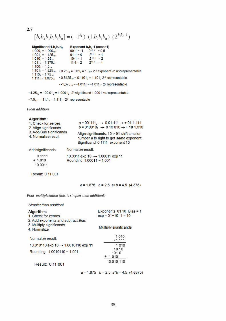
2.5 IEEE-754 standard for storage of 32-bit float. Assume that a 32-bit float is stored in a register: 40C8000016 What real decimal number is this? (2.6) Floating point format's principles becomes more transparent if one of pedagogical reasons "scales down" to a 4-bit register size (Nibble). However, a 4-bit format would be practically unusable. Assume the following four bit floating point format: )2().1()1(][ 1
00123123 −⋅⋅−= bbb bbbbb
The sign is expressed with the bit b3, the mantissa is represented by one bit b0, and the exponent has two bits b2b1 expressed as exess -1. a) Count up the number that can be represented with full precision. Mark them on the number line. b) How big is the largest quantization error? c) Can the number 0 be represented? If not, suggest a change in the format so that 0 can be represented. (2.7) To examine the addition and multiplication of floating point, we assume now for pedagogical reasons a 6 bit format. (This is still to few bits to be practically usable).
)2().1()1(][ 1012012345
345 −⋅⋅−= bbb bbbbbbbbb a) Which of the following numbers can be represented in this format? 0,25 0,8125 -1,375 4,25 7.5 b) Add the numbers (b5b4b3b2b1b0) 001111 and 010010. What is needed to avoid loss of precision? c) Multiply the previous numbers with each other.
5
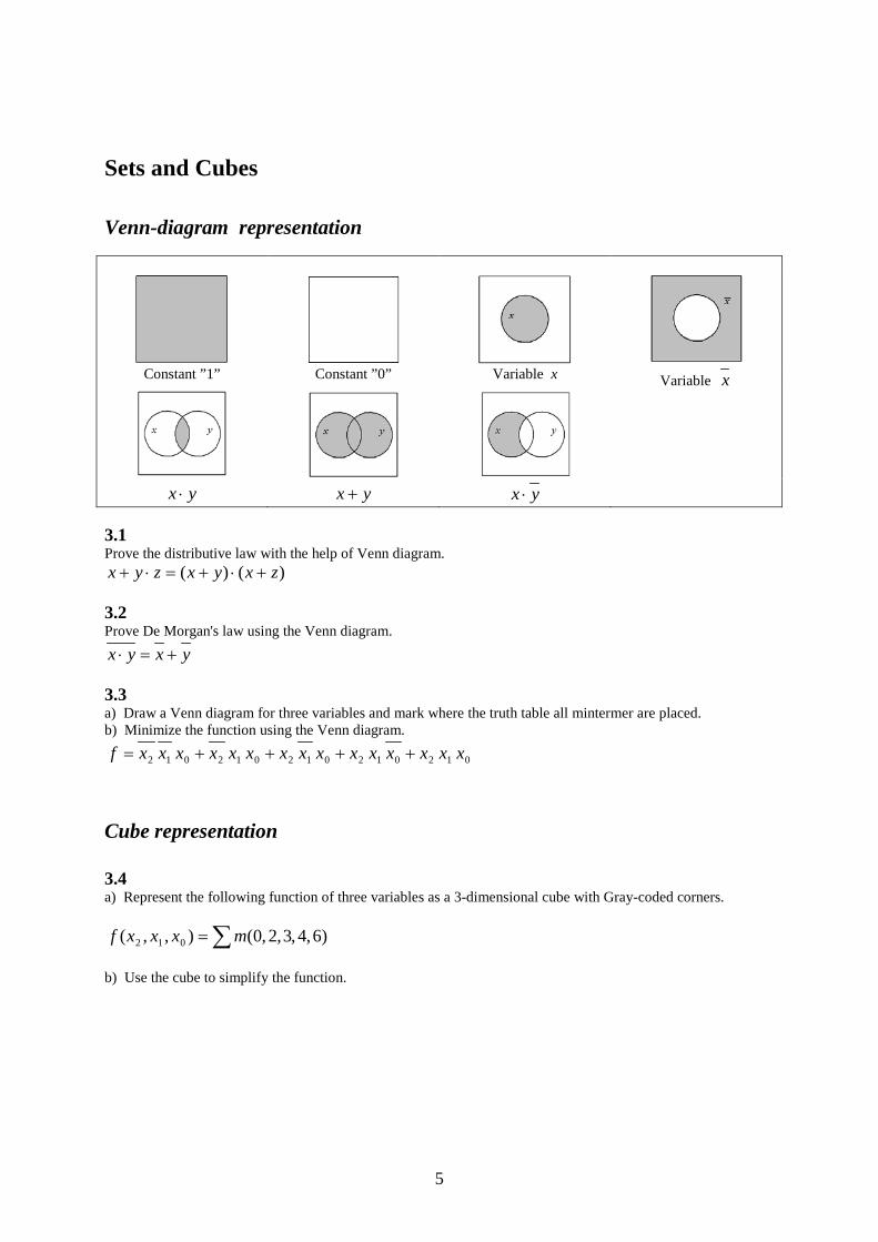
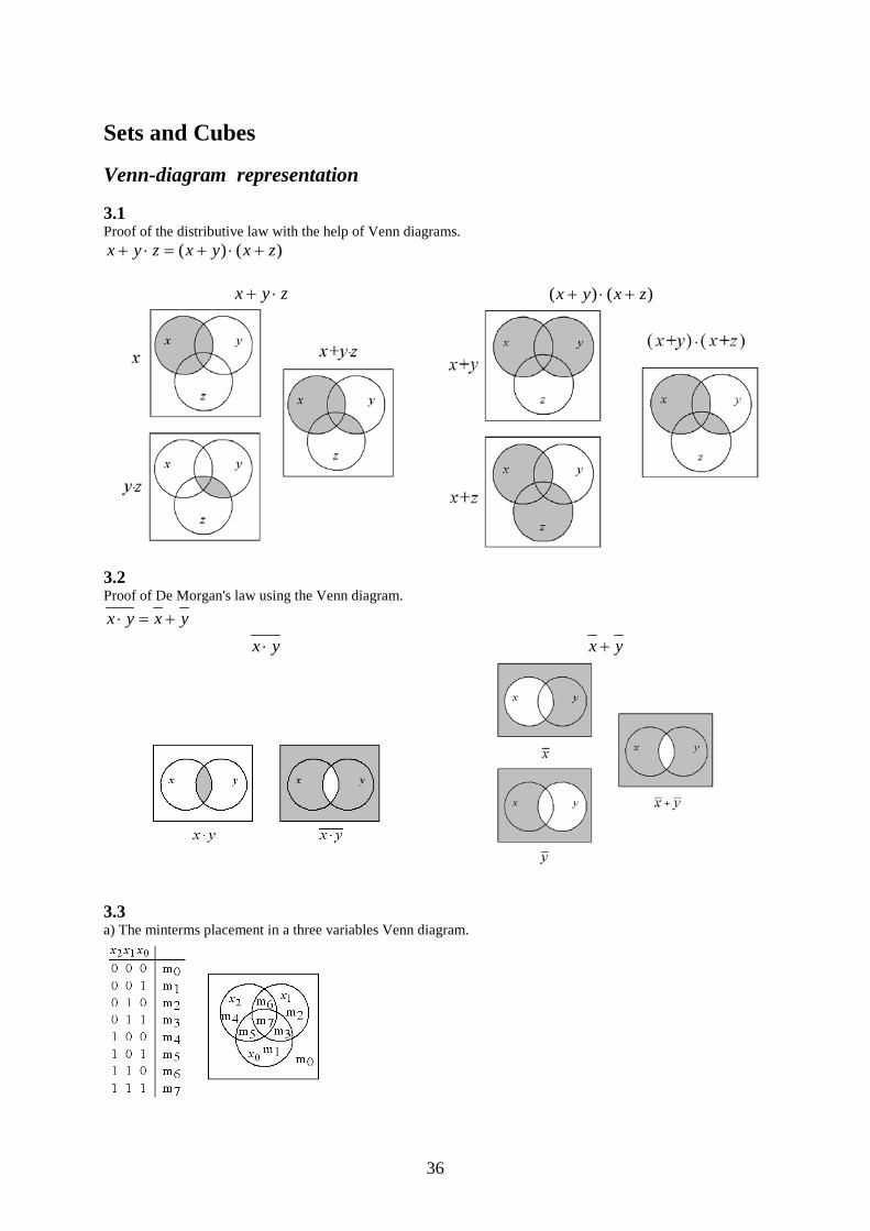
Sets and Cubes Venn-diagram representation
Constant ”1” Constant ”0” Variable x Variable x
yx ⋅ yx + yx ⋅ 3.1 Prove the distributive law with the help of Venn diagram.
)()( zxyxzyx +⋅+=⋅+ 3.2 Prove De Morgan's law using the Venn diagram.
yxyx +=⋅ 3.3 a) Draw a Venn diagram for three variables and mark where the truth table all mintermer are placed. b) Minimize the function using the Venn diagram.
012012012012012 xxxxxxxxxxxxxxxf ++++= Cube representation
3.4 a) Represent the following function of three variables as a 3-dimensional cube with Gray-coded corners.
∑= )6,4,3,2,0(),,( 012 mxxxf b) Use the cube to simplify the function.
6
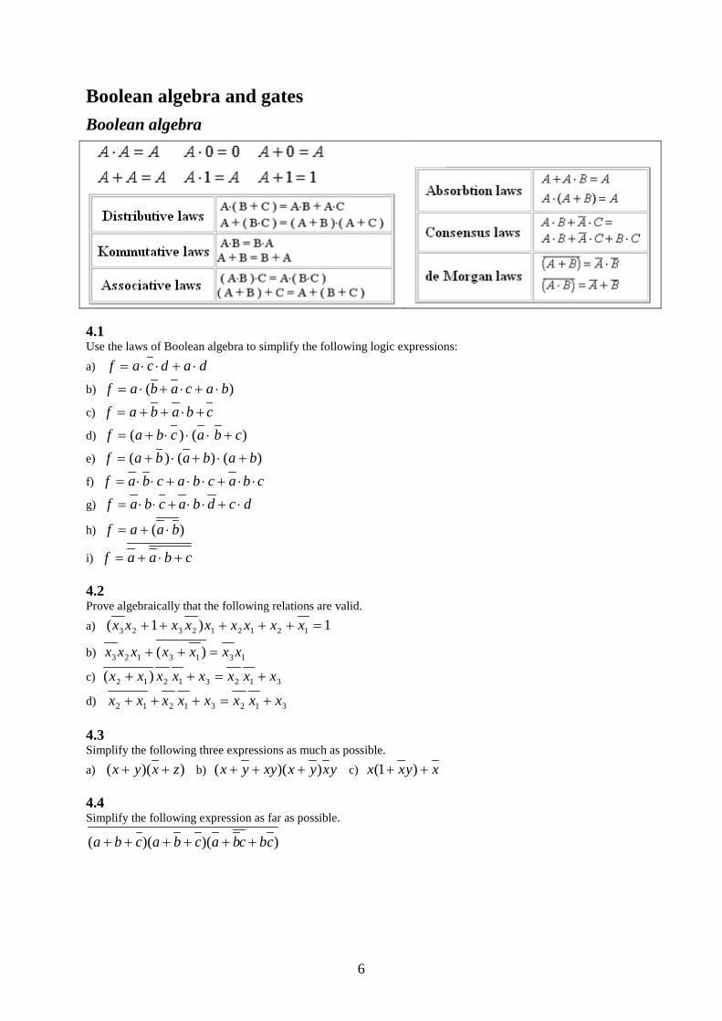
Boolean algebra and gates Boolean algebra
4.1 Use the laws of Boolean algebra to simplify the following logic expressions:
a) dadcaf ⋅+⋅⋅=
b) )( bacabaf ⋅+⋅+⋅=
c) cbabaf +⋅++=
d) )()( cbacbaf +⋅⋅⋅+=
e) )()()( bababaf +⋅+⋅+=
f) cbacbacbaf ⋅⋅+⋅⋅+⋅⋅=
g) dcdbacbaf ⋅+⋅⋅+⋅⋅=
h) )( baaf ⋅+=
i) cbaaf +⋅+= 4.2 Prove algebraically that the following relations are valid.
a) 1)1( 121212323 =+++++ xxxxxxxxx
b) 1313123 )( xxxxxxx =++
c) 31231212 )( xxxxxxxx +=++
d) 31231212 xxxxxxxx +=+++ 4.3 Simplify the following three expressions as much as possible. a) ))(( zxyx ++ b) yxyxxyyx ))(( +++ c) xyxx ++ )1( 4.4 Simplify the following expression as far as possible.
))()(( cbcbacbacba ++++++
7
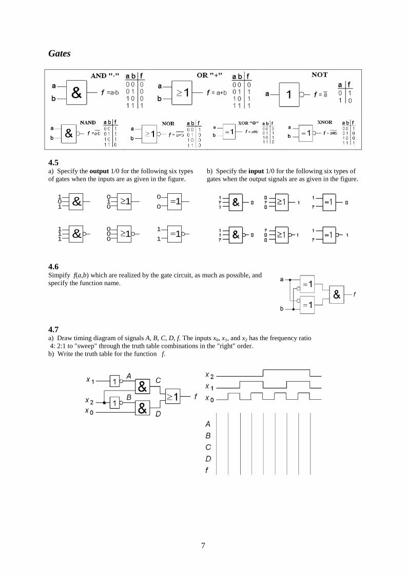
Gates
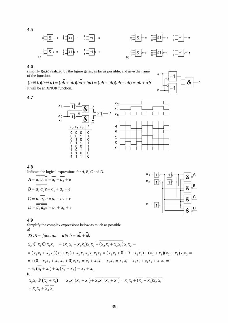
4.5 a) Specify the output 1/0 for the following six types of gates when the inputs are as given in the figure.
b) Specify the input 1/0 for the following six types of gates when the output signals are as given in the figure.
& ≥100
010
0=
& ≥1000
1=111
1
11
1
1
4.6 Simpify f(a,b) which are realized by the gate circuit, as much as possible, and specify the function name.
4.7 a) Draw timing diagram of signals A, B, C, D, f. The inputs x0, x1, and x2 has the frequency ratio 4: 2:1 to "sweep" through the truth table combinations in the "right" order. b) Write the truth table for the function f.
8
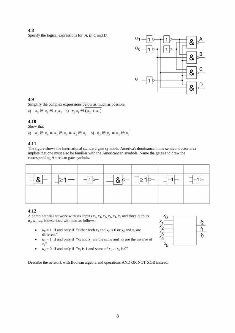
4.8 Specify the logical expressions for A, B, C and D.
4.9 Simplify the complex expressions below as much as possible.
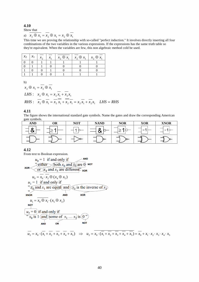
a) 2112 xxxx ⊕⊕ b) )( 1212 xxxx +⊕ 4.10 Show that
a) 121212 xxxxxx ⊕=⊕=⊕ b) 1212 xxxx ⊕=⊕ 4.11 The figure shows the international standard gate symbols. America's dominance in the semiconductor area implies that one must also be familiar with the Americancan symbols. Name the gates and draw the corresponding American gate symbols.
4.12 A combinatorial network with six inputs x5, x4, x3, x2, x1, x0 and three outputs u2, u1, u0, is described with text as follows:
• u0 = 1 if and only if ”either both x0 and x2 is 0 or x4 and x5 are different”
• u1 = 1 if and only if ”x0 and x1 are the same and x5 are the inverse of x2”
• u2 = 0 if and only if ”x0 is 1 and some of x1 ... x5 is 0”
Describe the network with Boolean algebra and operations AND OR NOT XOR instead.
9
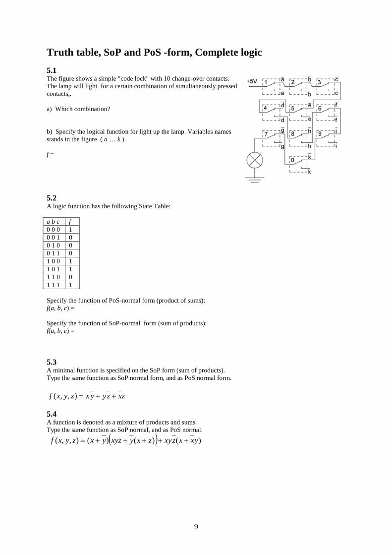
Truth table, SoP and PoS -form, Complete logic 5.1 The figure shows a simple "code lock" with 10 change-over contacts. The lamp will light for a certain combination of simultaneously pressed contacts,. a) Which combination? b) Specify the logical function for light up the lamp. Variables names stands in the figure ( a … k ). f =
5.2 A logic function has the following State Table: a b c f 0 0 0 1 0 0 1 0 0 1 0 0 0 1 1 0 1 0 0 1 1 0 1 1 1 1 0 0 1 1 1 1 Specify the function of PoS-normal form (product of sums): f(a, b, c) = Specify the function of SoP-normal form (sum of products): f(a, b, c) = 5.3 A minimal function is specified on the SoP form (sum of products). Type the same function as SoP normal form, and as PoS normal form.
zxzyyxzyxf ++=),,( 5.4 A function is denoted as a mixture of products and sums. Type the same function as SoP normal, and as PoS normal.
( ) )()()(),,( yxxzxyzxyxyzyxzyxf +++++=
10
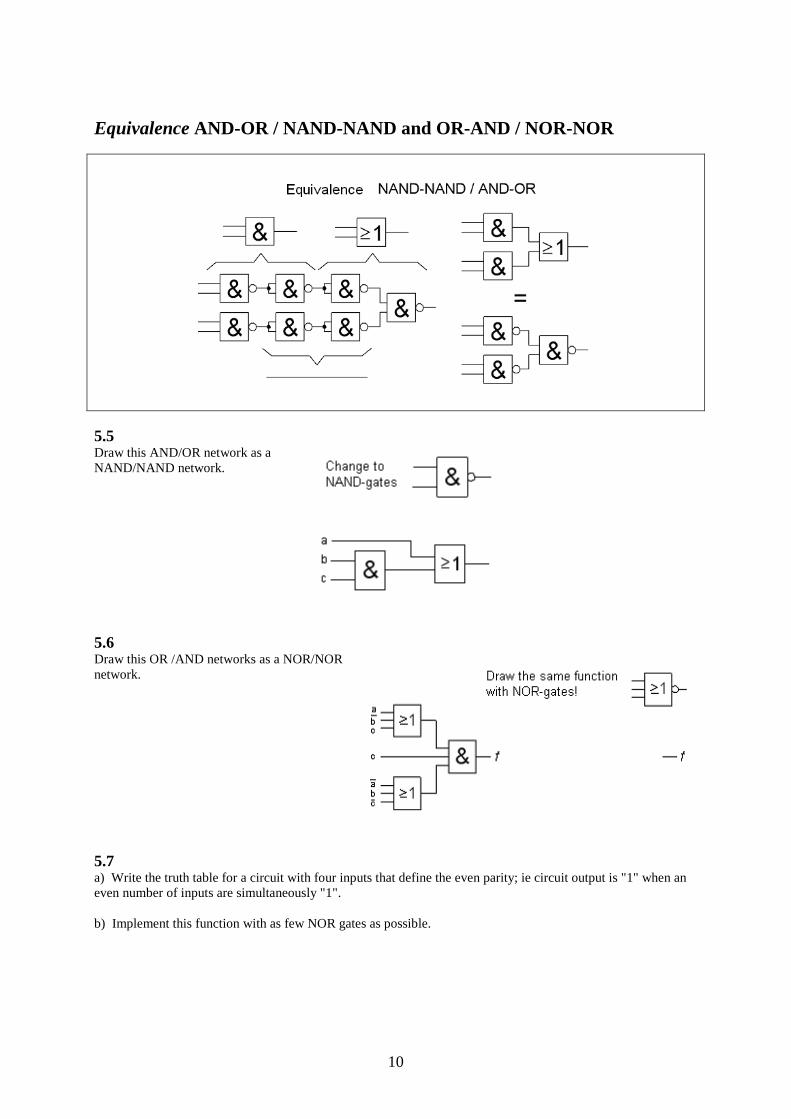
Equivalence AND-OR / NAND-NAND and OR-AND / NOR-NOR
5.5 Draw this AND/OR network as a NAND/NAND network.
5.6 Draw this OR /AND networks as a NOR/NOR network.
5.7 a) Write the truth table for a circuit with four inputs that define the even parity; ie circuit output is "1" when an even number of inputs are simultaneously "1". b) Implement this function with as few NOR gates as possible.
11
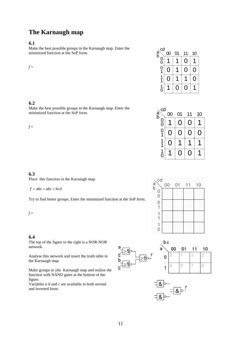
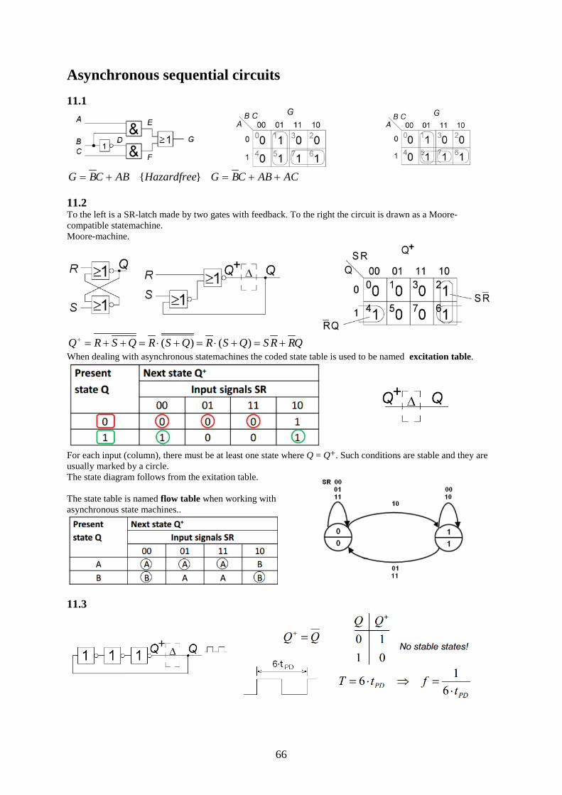
The Karnaugh map 6.1 Make the best possible groups in the Karnaugh map. Enter the minimized function at the SoP form. f =
00ab
cd01 11 10
00
1110
01
0
000
0 0 01
1 1
1
1 111
0
6.2 Make the best possible groups in the Karnaugh map. Enter the minimized function at the SoP form. f =
00ab
cd01 11 10
00
1110
01
00
000
0 0 001
1 1
1
1 1 1
6.3 Place this function in the Karnaugh map. f abc abc bcd= + +
Try to find better groups. Enter the minimized function at the SoP form. f =
6.4 The top of the figure to the right is a NOR-NOR network. Analyse this network and insert the truth table in the Karnaugh map. Make groups in yhe Karnaugh map and realize the function with NAND gates at the bottom of the figure. Variables a b and c are available in both normal and inverted form.
12
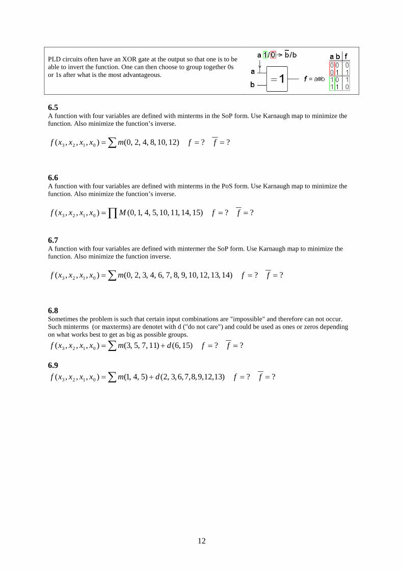
PLD circuits often have an XOR gate at the output so that one is to be able to invert the function. One can then choose to group together 0s or 1s after what is the most advantageous.
6.5 A function with four variables are defined with minterms in the SoP form. Use Karnaugh map to minimize the function. Also minimize the function’s inverse.
??)12,10,8,4,2,0(),,,( 0123 === ∑ ffmxxxxf 6.6 A function with four variables are defined with minterms in the PoS form. Use Karnaugh map to minimize the function. Also minimize the function’s inverse.
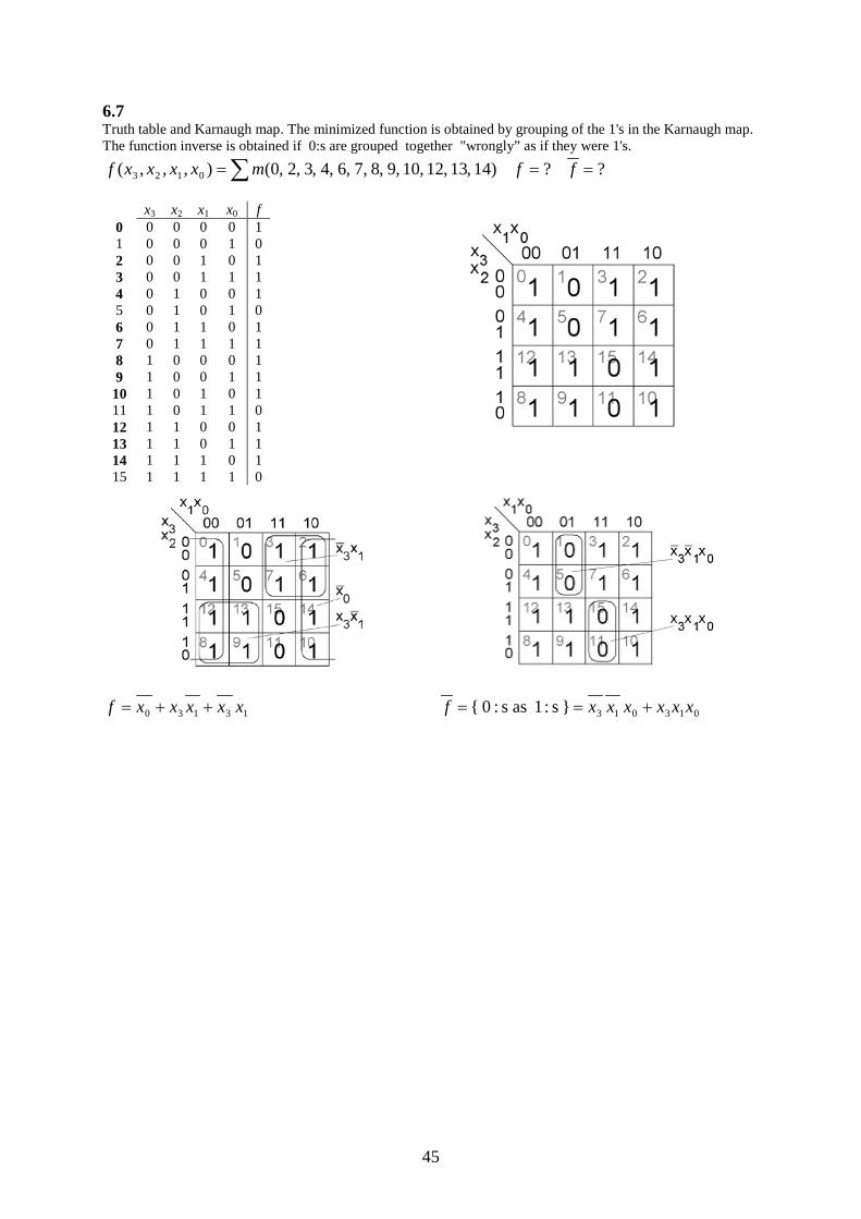
??)15,14,11,10,5,4,1,0(),,,( 0123 ===∏ ffMxxxxf 6.7 A function with four variables are defined with mintermer the SoP form. Use Karnaugh map to minimize the function. Also minimize the function inverse.
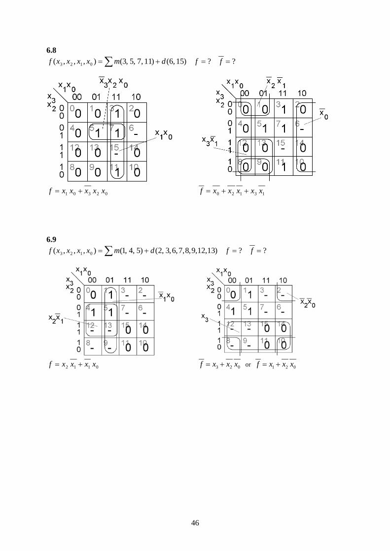
??)14,13,12,10,9,8,7,6,4,3,2,0(),,,( 0123 === ∑ ffmxxxxf 6.8 Sometimes the problem is such that certain input combinations are "impossible" and therefore can not occur. Such minterms (or maxterms) are denotet with d ("do not care") and could be used as ones or zeros depending on what works best to get as big as possible groups.
??)15,6()11,7,5,3(),,,( 0123 ==+= ∑ ffdmxxxxf 6.9
??)13,12,9,8,7,6,3,2()5,4,1(),,,( 0123 ==+= ∑ ffdmxxxxf
13
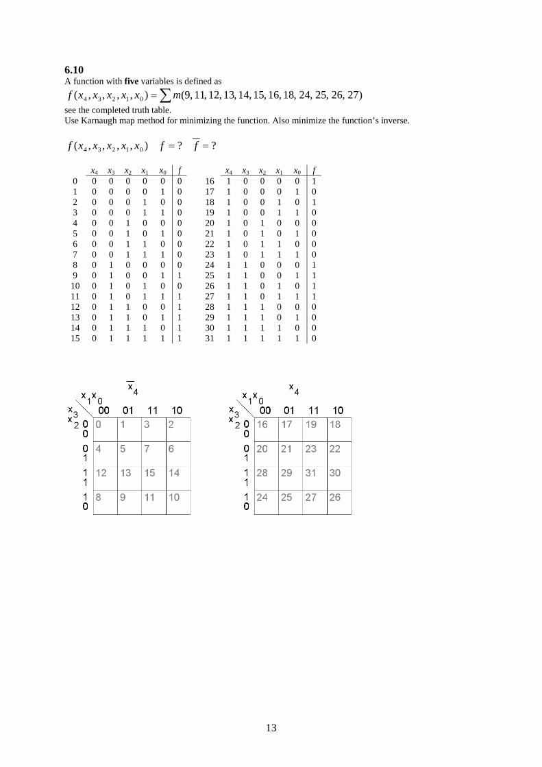
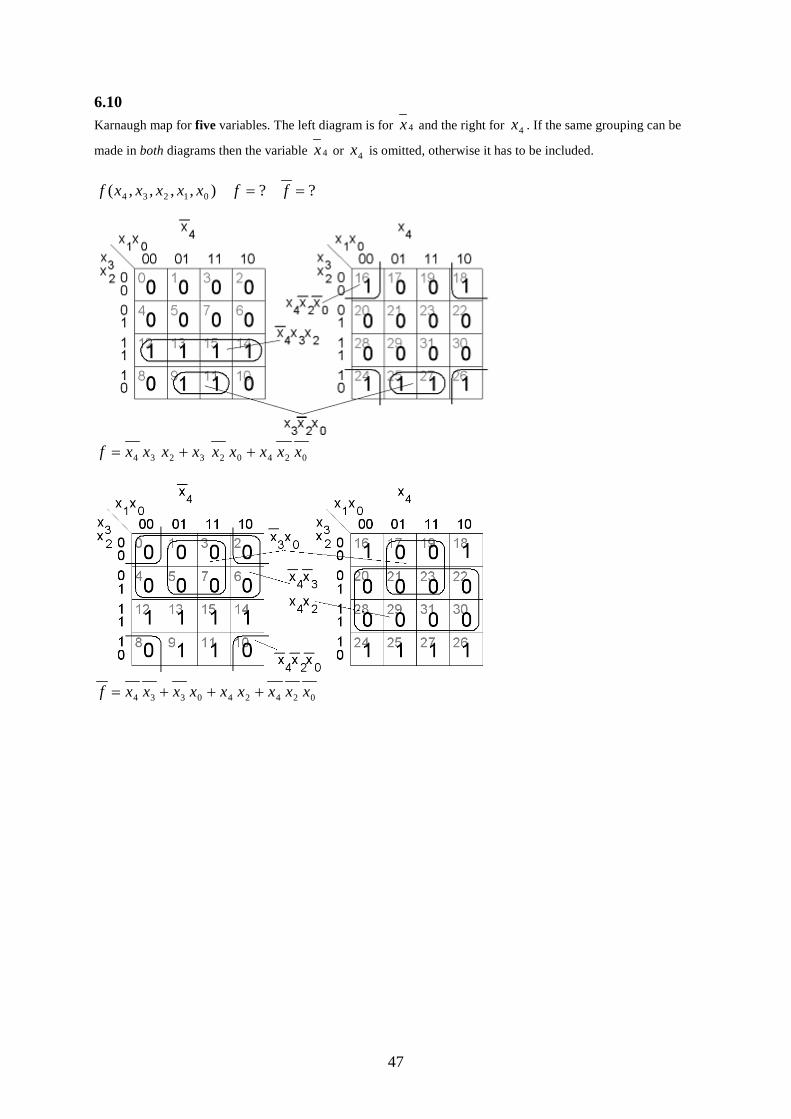
6.10 A function with five variables is defined as
∑= )27,26,25,24,18,16,15,14,13,12,11,9(),,,,( 01234 mxxxxxf see the completed truth table. Use Karnaugh map method for minimizing the function. Also minimize the function’s inverse.
??),,,,( 01234 == ffxxxxxf
x4 x3 x2 x1 x0 f 0 0 0 0 0 0 0 1 0 0 0 0 1 0 2 0 0 0 1 0 0 3 0 0 0 1 1 0 4 0 0 1 0 0 0 5 0 0 1 0 1 0 6 0 0 1 1 0 0 7 0 0 1 1 1 0 8 0 1 0 0 0 0 9 0 1 0 0 1 1 10 0 1 0 1 0 0 11 0 1 0 1 1 1 12 0 1 1 0 0 1 13 0 1 1 0 1 1 14 0 1 1 1 0 1 15 0 1 1 1 1 1
x4 x3 x2 x1 x0 f 16 1 0 0 0 0 1 17 1 0 0 0 1 0 18 1 0 0 1 0 1 19 1 0 0 1 1 0 20 1 0 1 0 0 0 21 1 0 1 0 1 0 22 1 0 1 1 0 0 23 1 0 1 1 1 0 24 1 1 0 0 0 1 25 1 1 0 0 1 1 26 1 1 0 1 0 1 27 1 1 0 1 1 1 28 1 1 1 0 0 0 29 1 1 1 0 1 0 30 1 1 1 1 0 0 31 1 1 1 1 1 0
14
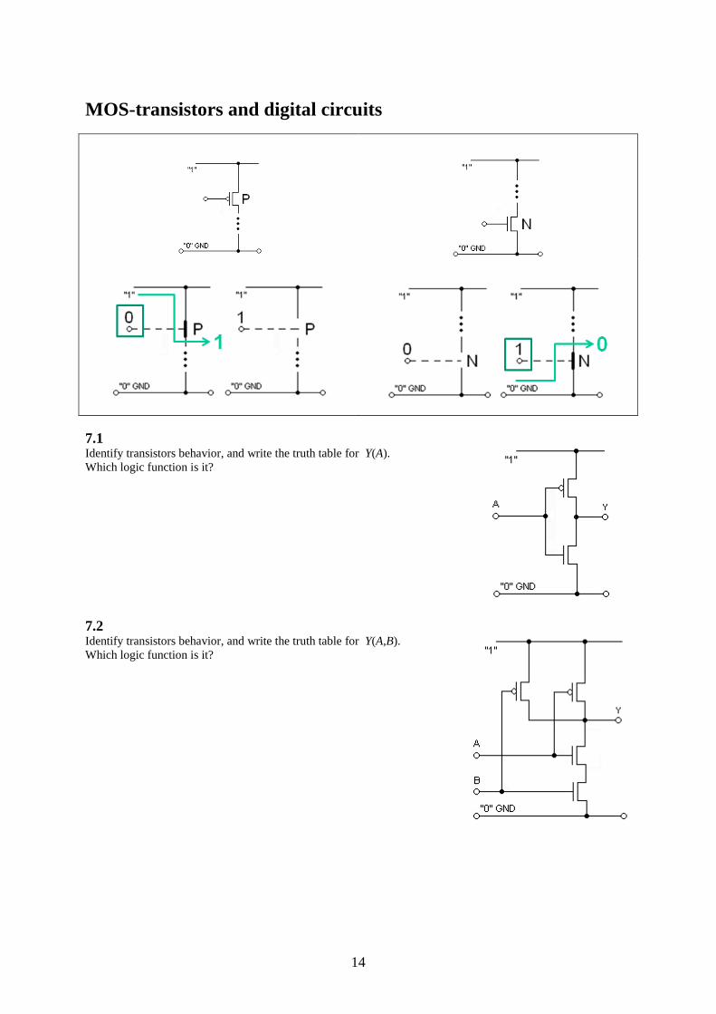
MOS-transistors and digital circuits
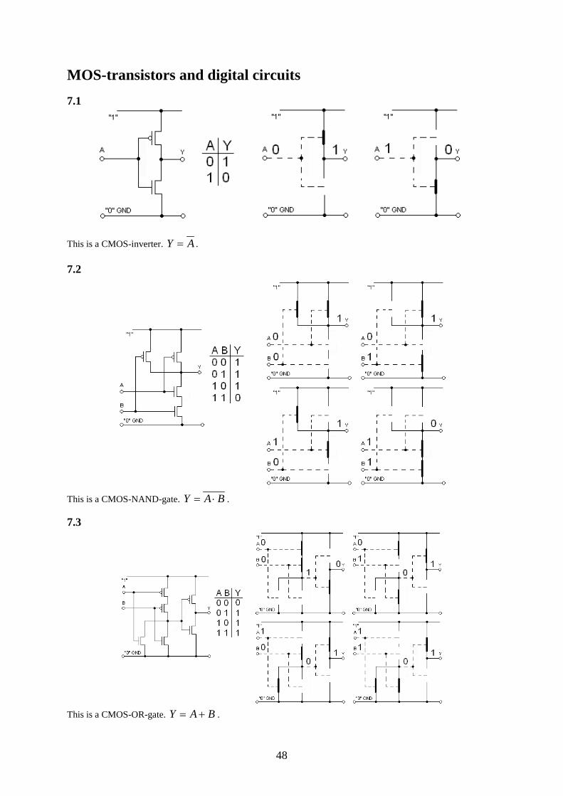
7.1 Identify transistors behavior, and write the truth table for Y(A). Which logic function is it?
7.2 Identify transistors behavior, and write the truth table for Y(A,B). Which logic function is it?
15
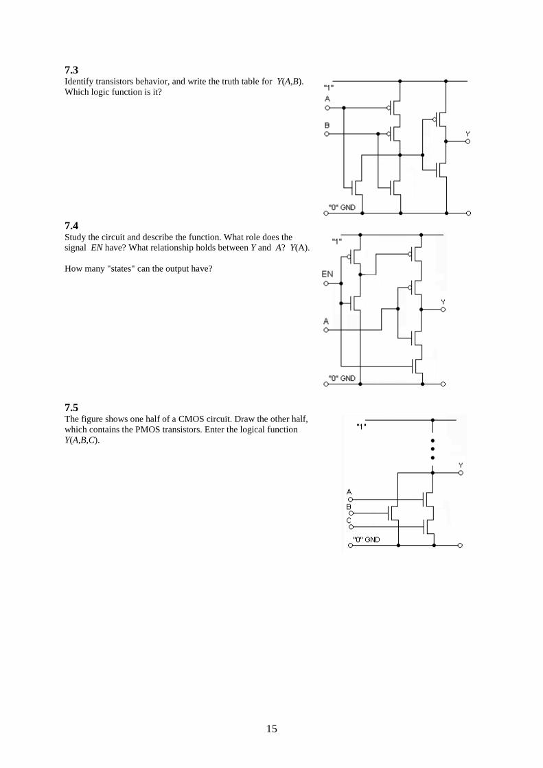
7.3 Identify transistors behavior, and write the truth table for Y(A,B). Which logic function is it?
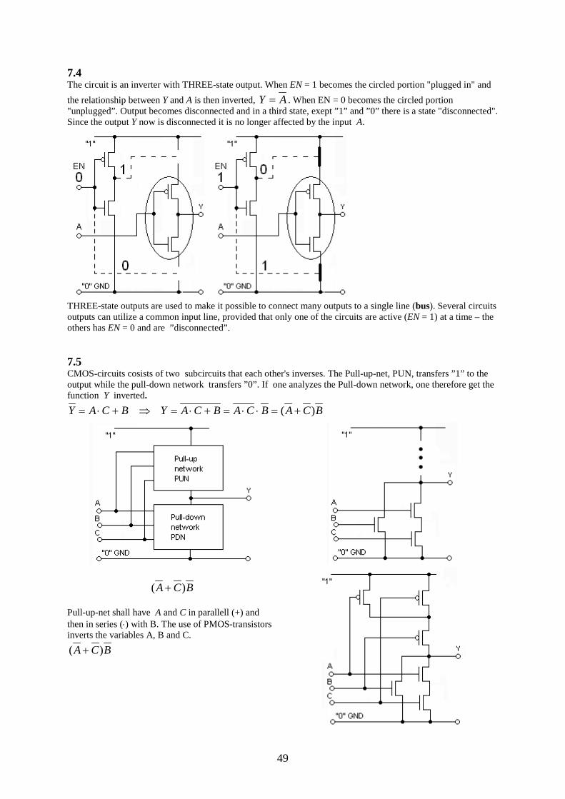
7.4 Study the circuit and describe the function. What role does the signal EN have? What relationship holds between Y and A? Y(A). How many "states" can the output have?
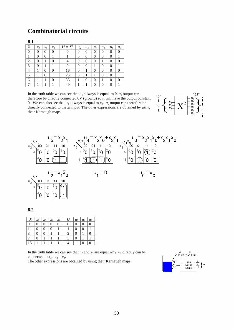
7.5 The figure shows one half of a CMOS circuit. Draw the other half, which contains the PMOS transistors. Enter the logical function Y(A,B,C).
16
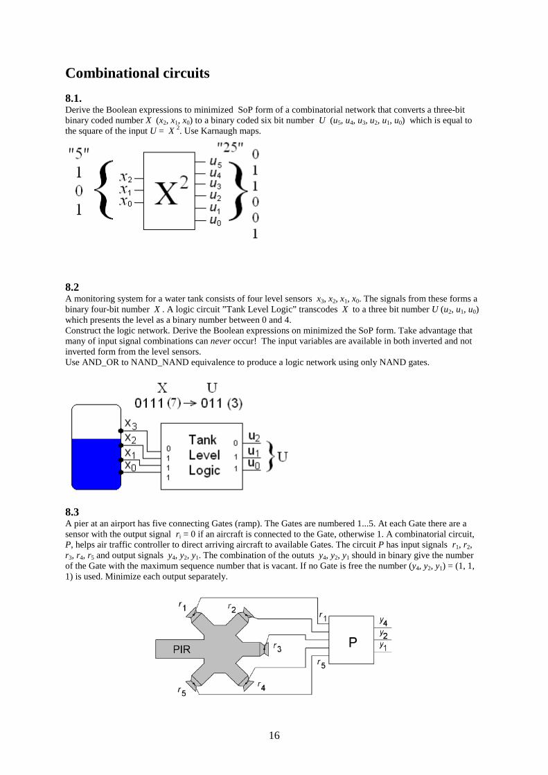
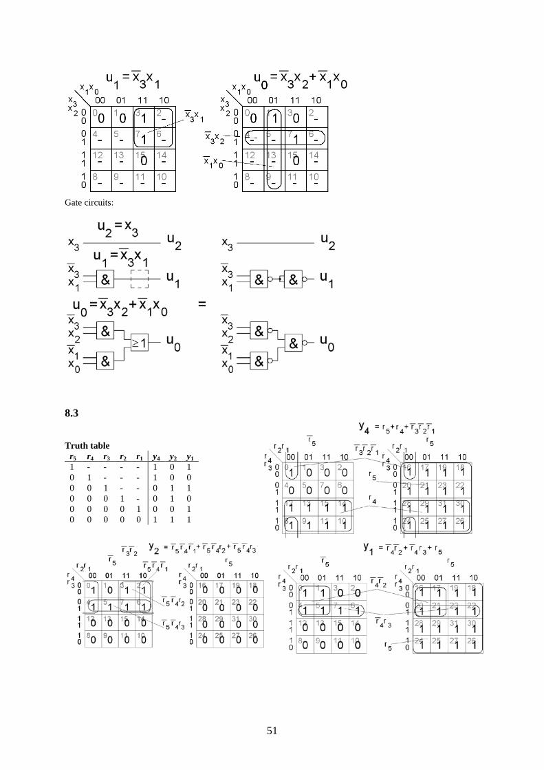
Combinational circuits 8.1. Derive the Boolean expressions to minimized SoP form of a combinatorial network that converts a three-bit binary coded number X (x2, x1, x0) to a binary coded six bit number U (u5, u4, u3, u2, u1, u0) which is equal to the square of the input U = X 2. Use Karnaugh maps.
8.2 A monitoring system for a water tank consists of four level sensors x3, x2, x1, x0. The signals from these forms a binary four-bit number X . A logic circuit ”Tank Level Logic” transcodes X to a three bit number U (u2, u1, u0) which presents the level as a binary number between 0 and 4. Construct the logic network. Derive the Boolean expressions on minimized the SoP form. Take advantage that many of input signal combinations can never occur! The input variables are available in both inverted and not inverted form from the level sensors. Use AND_OR to NAND_NAND equivalence to produce a logic network using only NAND gates.
8.3 A pier at an airport has five connecting Gates (ramp). The Gates are numbered 1...5. At each Gate there are a sensor with the output signal ri = 0 if an aircraft is connected to the Gate, otherwise 1. A combinatorial circuit, P, helps air traffic controller to direct arriving aircraft to available Gates. The circuit P has input signals r1, r2, r3, r4, r5 and output signals y4, y2, y1. The combination of the oututs y4, y2, y1 should in binary give the number of the Gate with the maximum sequence number that is vacant. If no Gate is free the number (y4, y2, y1) = (1, 1, 1) is used. Minimize each output separately.
17
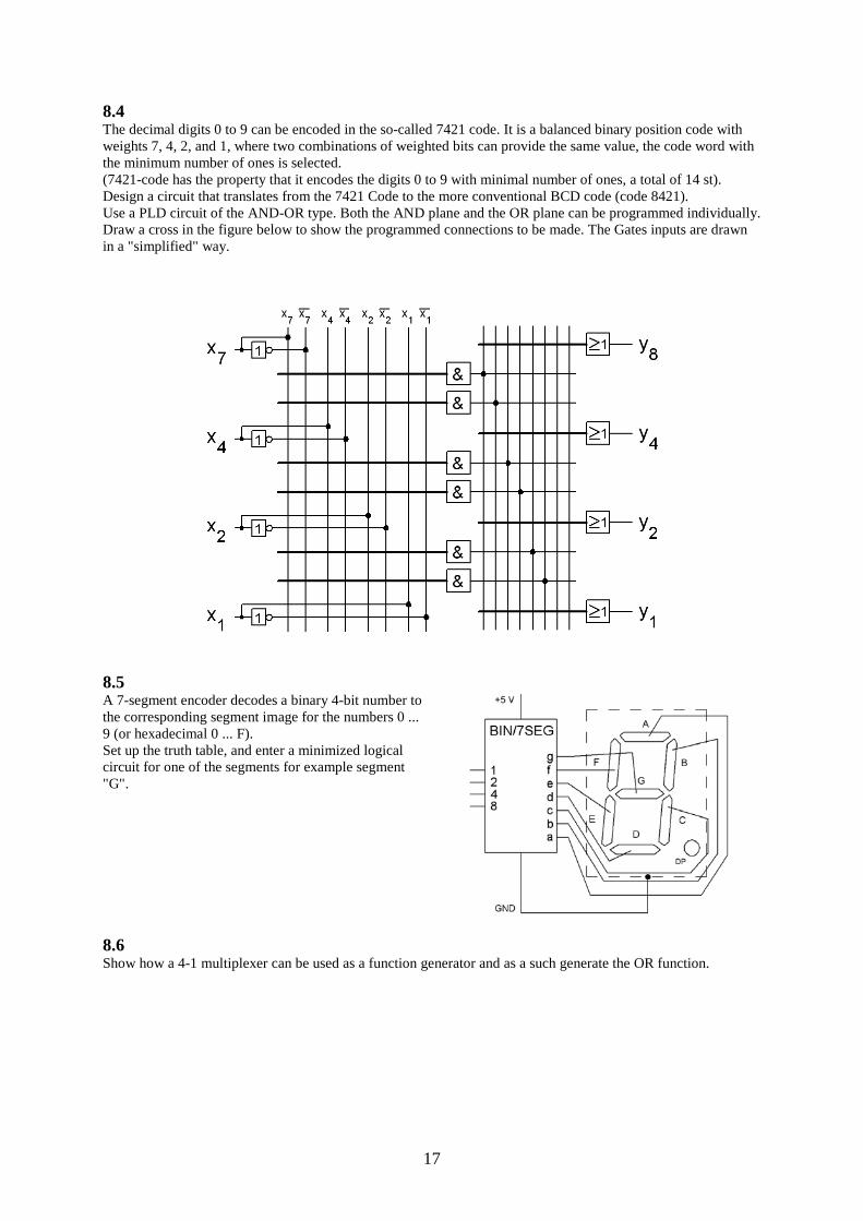
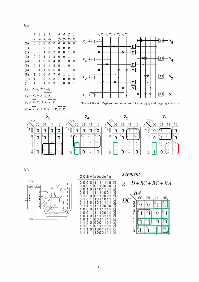
8.4 The decimal digits 0 to 9 can be encoded in the so-called 7421 code. It is a balanced binary position code with weights 7, 4, 2, and 1, where two combinations of weighted bits can provide the same value, the code word with the minimum number of ones is selected. (7421-code has the property that it encodes the digits 0 to 9 with minimal number of ones, a total of 14 st). Design a circuit that translates from the 7421 Code to the more conventional BCD code (code 8421). Use a PLD circuit of the AND-OR type. Both the AND plane and the OR plane can be programmed individually. Draw a cross in the figure below to show the programmed connections to be made. The Gates inputs are drawn in a "simplified" way.
8.5 A 7-segment encoder decodes a binary 4-bit number to the corresponding segment image for the numbers 0 ... 9 (or hexadecimal 0 ... F). Set up the truth table, and enter a minimized logical circuit for one of the segments for example segment "G".
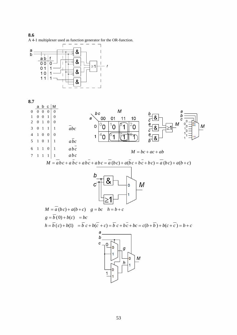
8.6 Show how a 4-1 multiplexer can be used as a function generator and as a such generate the OR function.
18
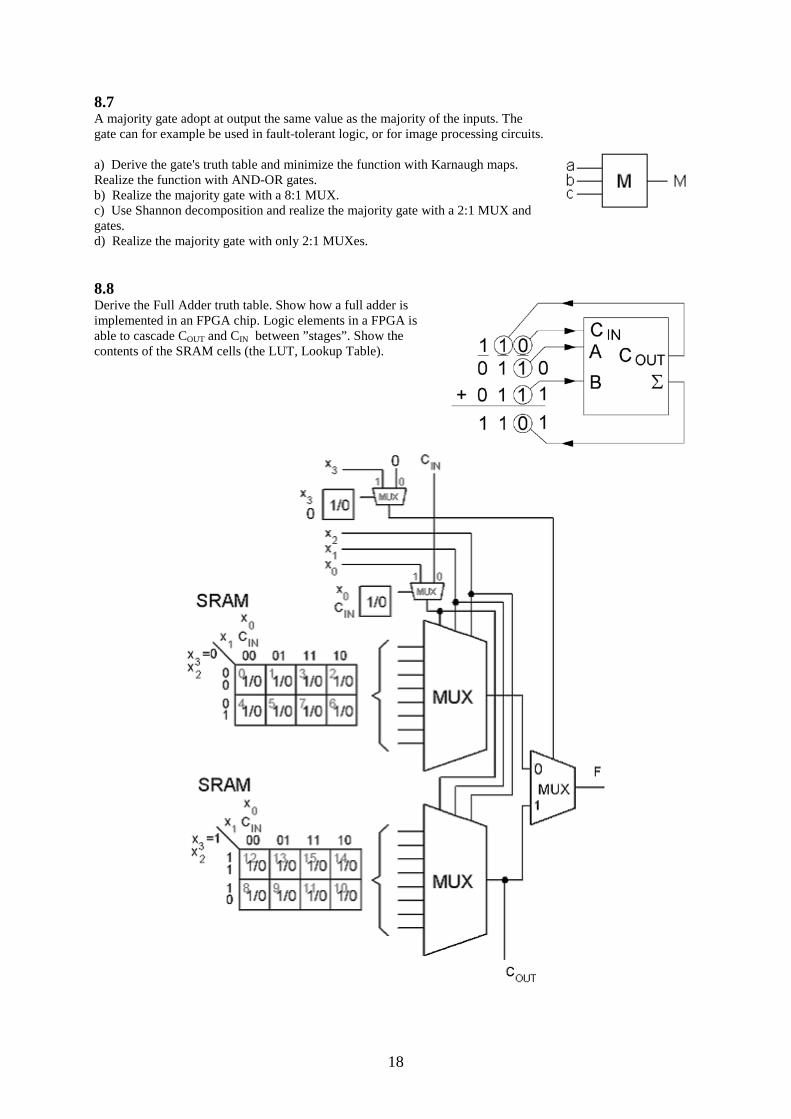
8.7 A majority gate adopt at output the same value as the majority of the inputs. The gate can for example be used in fault-tolerant logic, or for image processing circuits. a) Derive the gate's truth table and minimize the function with Karnaugh maps. Realize the function with AND-OR gates. b) Realize the majority gate with a 8:1 MUX. c) Use Shannon decomposition and realize the majority gate with a 2:1 MUX and gates. d) Realize the majority gate with only 2:1 MUXes.
8.8 Derive the Full Adder truth table. Show how a full adder is implemented in an FPGA chip. Logic elements in a FPGA is able to cascade COUT and CIN between ”stages”. Show the contents of the SRAM cells (the LUT, Lookup Table).

19
8.9 Show how one four-input XOR gate (XOR) are realized in a FPGA circuit. Show the contents of the SRAM cells (the LUT, Lookup Table).
20
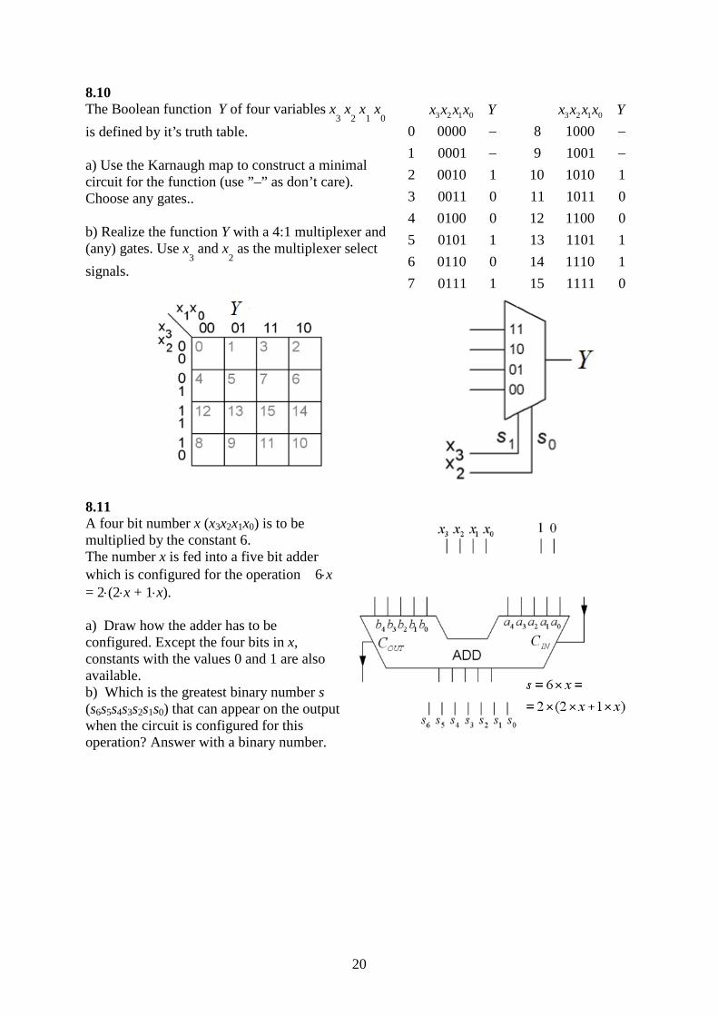
8.10 The Boolean function Y of four variables x
3 x
2 x
1 x
0
is defined by it’s truth table. a) Use the Karnaugh map to construct a minimal circuit for the function (use ”–” as don’t care). Choose any gates.. b) Realize the function Y with a 4:1 multiplexer and (any) gates. Use x
3 and x
2 as the multiplexer select
signals.
3 2 1 0 3 2 1 0
0 0000 8 10001 0001 9 10012 0010 1 10 1010 13 0011 0 11 1011 04 0100 0 12 1100 05 0101 1 13 1101 16 0110 0 14 1110 17 0111 1 15 1111 0
x x x x Y x x x x Y− −− −
8.11 A four bit number x (x3x2x1x0) is to be multiplied by the constant 6. The number x is fed into a five bit adder which is configured for the operation 6⋅x = 2⋅(2⋅x + 1⋅x). a) Draw how the adder has to be configured. Except the four bits in x, constants with the values 0 and 1 are also available. b) Which is the greatest binary number s (s6s5s4s3s2s1s0) that can appear on the output when the circuit is configured for this operation? Answer with a binary number.
21
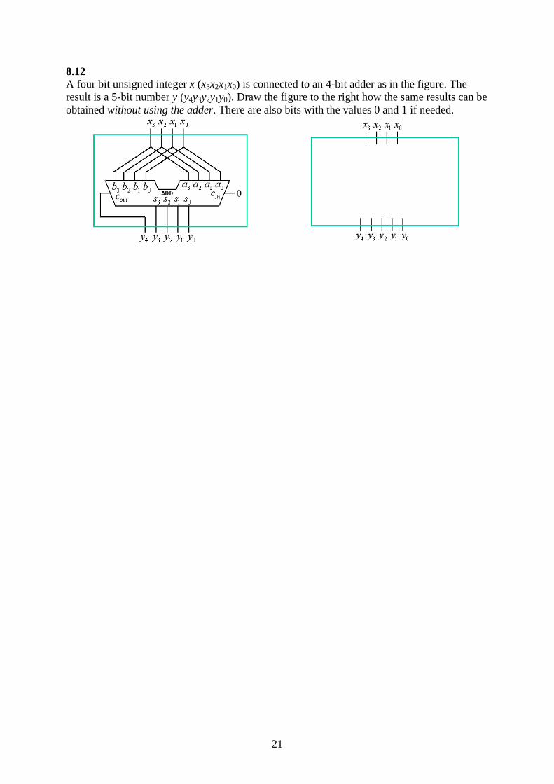
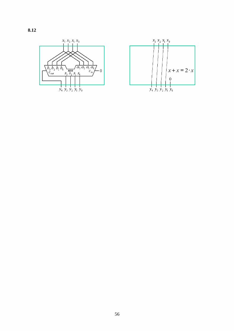
8.12 A four bit unsigned integer x (x3x2x1x0) is connected to an 4-bit adder as in the figure. The result is a 5-bit number y (y4y3y2y1y0). Draw the figure to the right how the same results can be obtained without using the adder. There are also bits with the values 0 and 1 if needed.
22
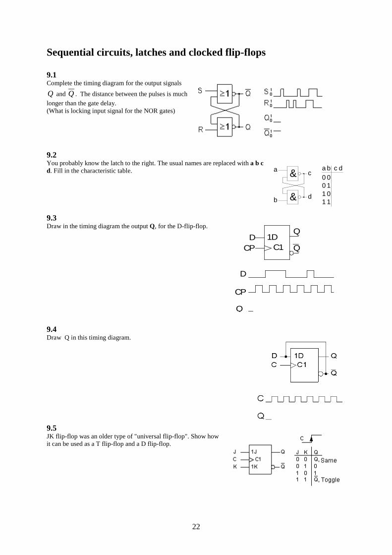
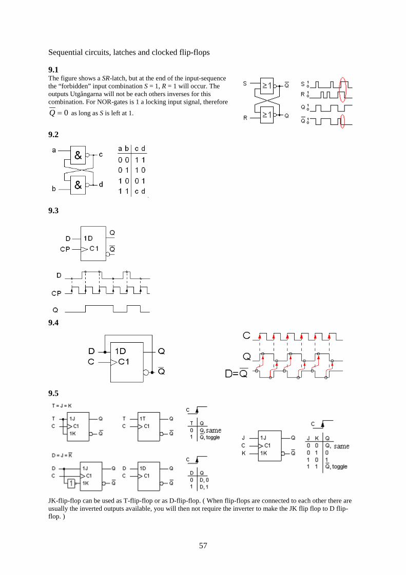
Sequential circuits, latches and clocked flip-flops 9.1 Complete the timing diagram for the output signals
Q and Q . The distance between the pulses is much longer than the gate delay. (What is locking input signal for the NOR gates)
9.2 You probably know the latch to the right. The usual names are replaced with a b c d. Fill in the characteristic table. &
&
a
b
c
d
a b c d0 00 11 01 1
9.3 Draw in the timing diagram the output Q, for the D-flip-flop.
C1CP1DD
Q
Q
D
CP
Q
9.4 Draw Q in this timing diagram.
9.5 JK flip-flop was an older type of "universal flip-flop". Show how it can be used as a T flip-flop and a D flip-flop.

23
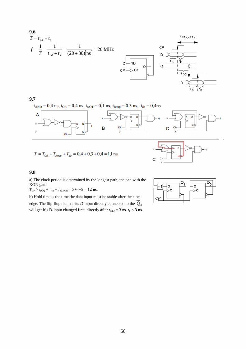
Flip-Flop Timing Parameters. The fip-flop is loaded with data at the positive edge of the clockpulse, but data must be stable ts before the clock edge and even the time th after. The data can be found at output after the time tpd. (tpd can be different for 0→1 respective 1→0 transitions). If these times are not respected the flip-flop functioning becomes uncertain. 9.6 What is the maximum clock frequency that can be used to the circuit in the figure without risking malfunction? Suppose ts = 20 ns th = 5 ns tpd = 30 ns
9.7 The figure shows three different state machines. Specify the state machine (A, B or C) that can operate at the highest clock speed. Highlight the critical path (the path that limits clock frequency) in this figure and calculate the period time for the clock signal Clk
9.8
For the flip-flops: setup time tsu = 4 ns, delay time for the flip-flop outputs tpdQ = 3 ns. The XOR-gate has delay time tpdXOR = 5 ns.
a) How long does it needs to be between the clock pulses TCP > ?, for the counter function to be safe?
b) What value must the hold time have th for this circuit to work? th < ? ns.
24
Sequential circuits
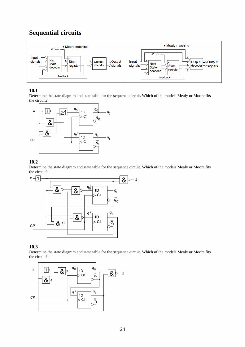
10.1 Determine the state diagram and state table for the sequence circuit. Which of the models Mealy or Moore fits the circuit?
10.2 Determine the state diagram and state table for the sequence circuit. Which of the models Mealy or Moore fits the circuit?
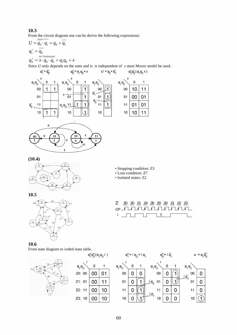
10.3 Determine the state diagram and state table for the sequence circuit. Which of the models Mealy or Moore fits the circuit?

25
(10.4) Is there any stopping condition, loss condition or isolated states in the state diagram? Stopping condition: Loss condition: • Isolated states:
10.5 To the right is a state diagram for a Moore machine. (it will detect a double tap). A monkey accidentally get hold of the push-button input signal, and then presses according to the timing diagram below. The Moore-machine has flip-flops that are triggered by the positive edge of the clock. Suppose that the initial state is Z0. Fill in the states the machine enters..
Z0 Z Z Z Z Z Z Z Z Z Z:CPi
10.6 Construct a Moore machine which requires that the input signal is equal to one ( i = 1 ) during three successive clock pulse interval, for the output to be one ( u = 1 ). As soon as the input signal becomes zero ( i = 0 ) during a clock pulse interval, the circuit output should return to zero ( u = 0 ). See the state diagram. Choose Gray code for state encoding. ( Z0=00, Z1=01, Z2=11, Z3=10 ). Use D-flip-flops and AND-OR gates. ( This is a safety circuit to prevent "false alarms” )
26
10.7 Construct a sequential circuit that detects when the input signal x has a transition 1→0 and then has the output u = 1 in the following clock-pulse interval, and then being 0 for the rest of the sequence. The circuit should be able to "reset" with an asynchronous reset pulse (NR active low), so that it monitors the input signal again.
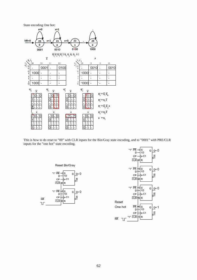
a) Draw state a diagram of a Moore machine type for the sequence network. b) Derive the Boolean expressions for the next state and the output for three different state encoding:: 1) ”Binarycode” 2) ”Graycode” 3) ”One hot” code c) Show how the reset signal is connected to NR D-flip-flops PRE and CLR inputs. 10.8
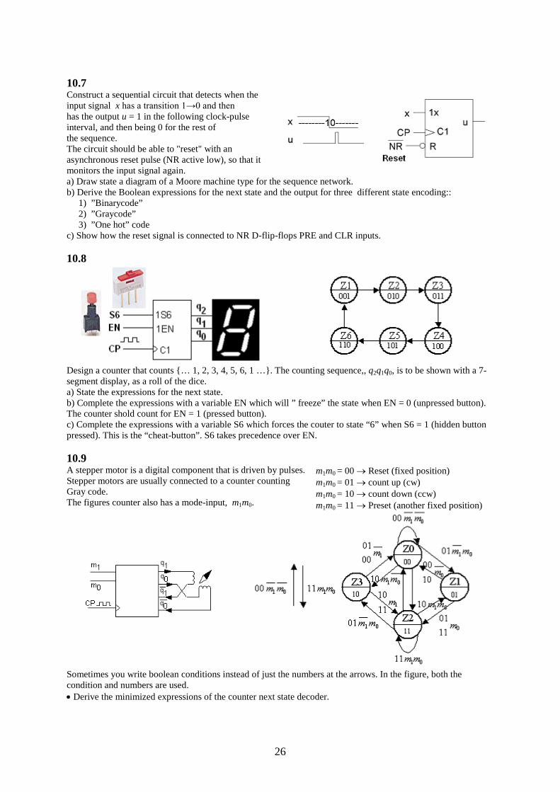
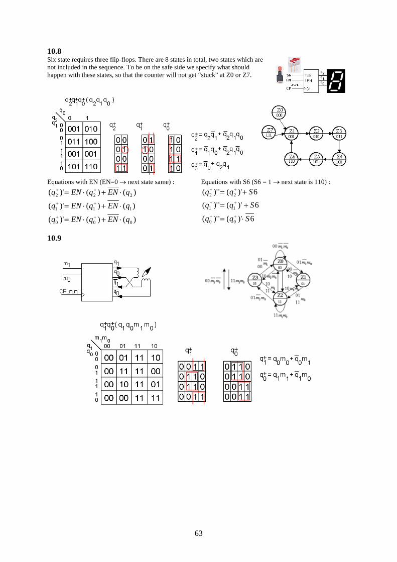
Design a counter that counts {… 1, 2, 3, 4, 5, 6, 1 …}. The counting sequence,, q2q1q0, is to be shown with a 7-segment display, as a roll of the dice. a) State the expressions for the next state. b) Complete the expressions with a variable EN which will ” freeze” the state when EN = 0 (unpressed button). The counter shold count for EN = 1 (pressed button). c) Complete the expressions with a variable S6 which forces the couter to state “6” when S6 = 1 (hidden button pressed). This is the “cheat-button”. S6 takes precedence over EN. 10.9 A stepper motor is a digital component that is driven by pulses. Stepper motors are usually connected to a counter counting Gray code. The figures counter also has a mode-input, m1m0.
m1m0 = 00 → Reset (fixed position) m1m0 = 01 → count up (cw) m1m0 = 10 → count down (ccw) m1m0 = 11 → Preset (another fixed position)
Sometimes you write boolean conditions instead of just the numbers at the arrows. In the figure, both the condition and numbers are used. • Derive the minimized expressions of the counter next state decoder.
27
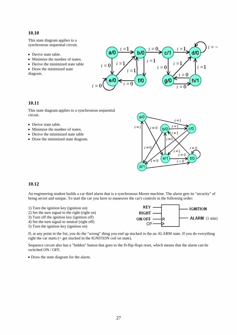
10.10 This state diagram applies to a synchronous sequential circuit. • Derive state table. • Minimize the number of states. • Derive the minimized state table • Draw the minimized state diagram.
10.11 This state diagram applies to a synchronous sequential circuit. • Derive state table. • Minimize the number of states. • Derive the minimized state table • Draw the minimized state diagram.
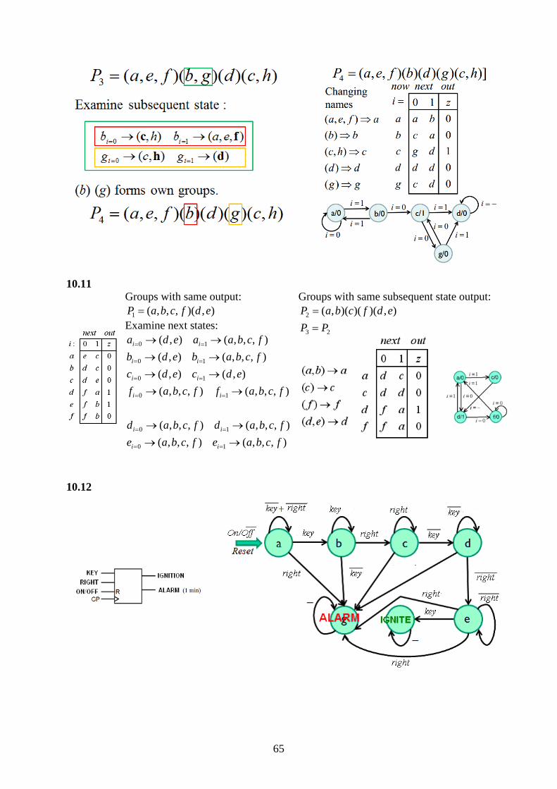
10.12
An engineering student builds a car thief alarm that is a synchronous Moore machine. The alarm gets its "security" of being secret and unique. To start the car you have to maneuver the car's controls in the following order:
1) Turn the ignition key (ignition on) 2) Set the turn signal to the right (right on) 3) Turn off the ignition key (ignition off) 4) Set the turn signal to neutral (right off) 5) Turn the ignition key (ignition on) If, at any point in the list, you do the "wrong" thing you end up stucked in the an ALARM state. If you do everything right the car starts (= get stucked in the IGNITION coil on state).
Sequence circuit also has a "hidden" button that goes to the D-flip-flops reset, which means that the alarm can be switched ON / OFF.
• Draw the state diagram for the alarm.
28
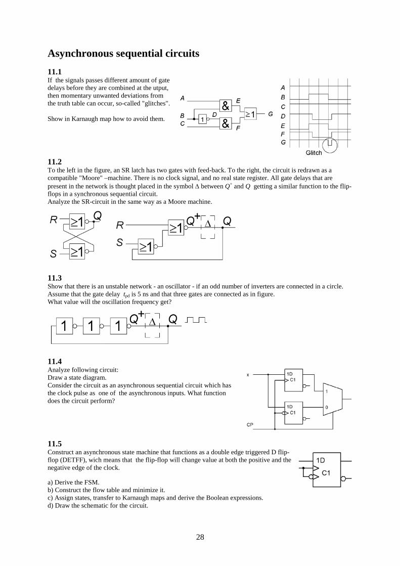
Asynchronous sequential circuits 11.1 If the signals passes different amount of gate delays before they are combined at the utput, then momentary unwanted deviations from the truth table can occur, so-called "glitches". Show in Karnaugh map how to avoid them.
11.2 To the left in the figure, an SR latch has two gates with feed-back. To the right, the circuit is redrawn as a compatible "Moore" –machine. There is no clock signal, and no real state register. All gate delays that are present in the network is thought placed in the symbol ∆ between Q+ and Q getting a similar function to the flip-flops in a synchronous sequential circuit. Analyze the SR-circuit in the same way as a Moore machine.
11.3 Show that there is an unstable network - an oscillator - if an odd number of inverters are connected in a circle. Assume that the gate delay tpd is 5 ns and that three gates are connected as in figure. What value will the oscillation frequency get?
11.4 Analyze following circuit: Draw a state diagram. Consider the circuit as an asynchronous sequential circuit which has the clock pulse as one of the asynchronous inputs. What function does the circuit perform?
11.5 Construct an asynchronous state machine that functions as a double edge triggered D flip-flop (DETFF), wich means that the flip-flop will change value at both the positive and the negative edge of the clock. a) Derive the FSM. b) Construct the flow table and minimize it. c) Assign states, transfer to Karnaugh maps and derive the Boolean expressions. d) Draw the schematic for the circuit.
29
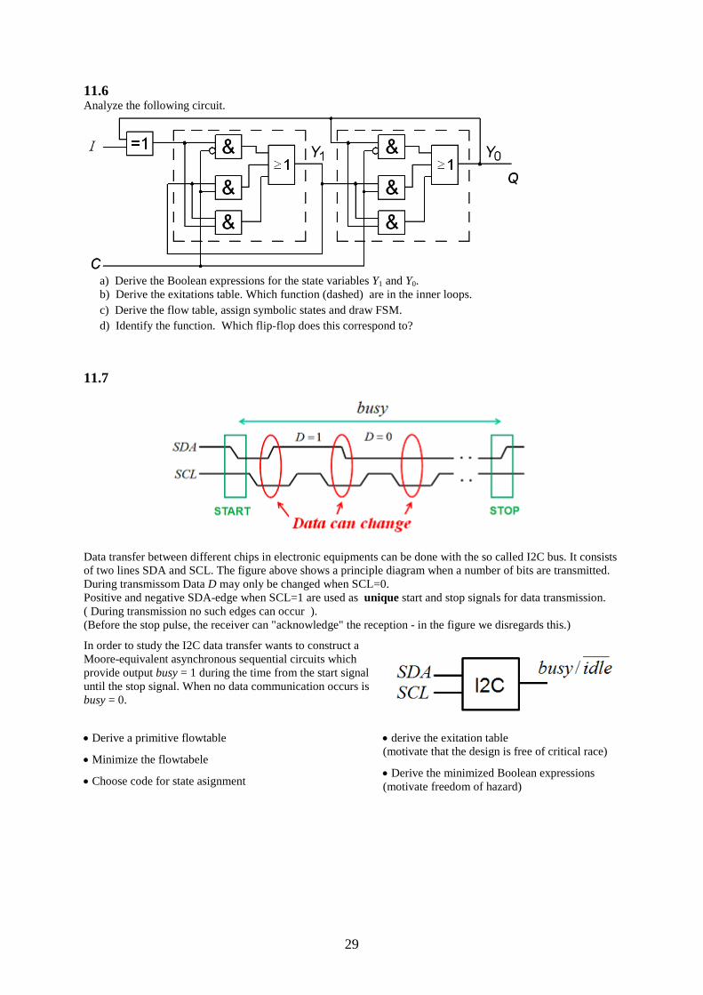
11.6 Analyze the following circuit.
a) Derive the Boolean expressions for the state variables Y1 and Y0. b) Derive the exitations table. Which function (dashed) are in the inner loops. c) Derive the flow table, assign symbolic states and draw FSM. d) Identify the function. Which flip-flop does this correspond to?
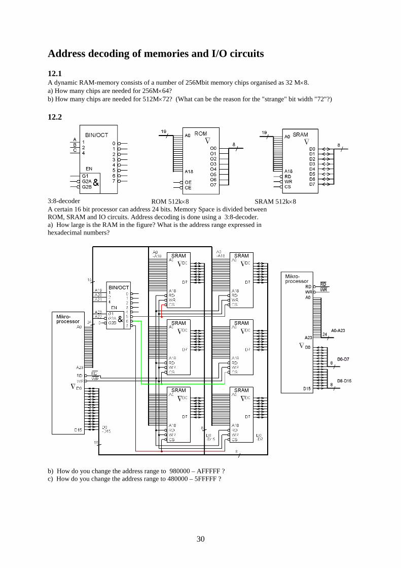
11.7
Data transfer between different chips in electronic equipments can be done with the so called I2C bus. It consists of two lines SDA and SCL. The figure above shows a principle diagram when a number of bits are transmitted. During transmissom Data D may only be changed when SCL=0. Positive and negative SDA-edge when SCL=1 are used as unique start and stop signals for data transmission. ( During transmission no such edges can occur ). (Before the stop pulse, the receiver can "acknowledge" the reception - in the figure we disregards this.)
In order to study the I2C data transfer wants to construct a Moore-equivalent asynchronous sequential circuits which provide output busy = 1 during the time from the start signal until the stop signal. When no data communication occurs is busy = 0.
• Derive a primitive flowtable
• Minimize the flowtabele
• Choose code for state asignment
• derive the exitation table (motivate that the design is free of critical race)
• Derive the minimized Boolean expressions (motivate freedom of hazard)
30
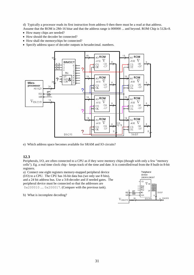
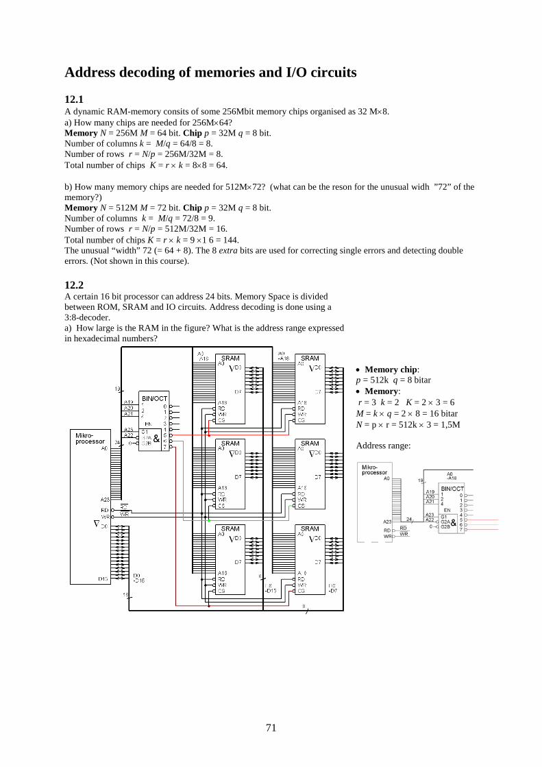
Address decoding of memories and I/O circuits 12.1 A dynamic RAM-memory consists of a number of 256Mbit memory chips organised as 32 M×8. a) How many chips are needed for 256M×64? b) How many chips are needed for 512M×72? (What can be the reason for the "strange" bit width "72"?) 12.2
3:8-decoder ROM 512k×8 SRAM 512k×8 A certain 16 bit processor can address 24 bits. Memory Space is divided between ROM, SRAM and IO circuits. Address decoding is done using a 3:8-decoder. a) How large is the RAM in the figure? What is the address range expressed in hexadecimal numbers?
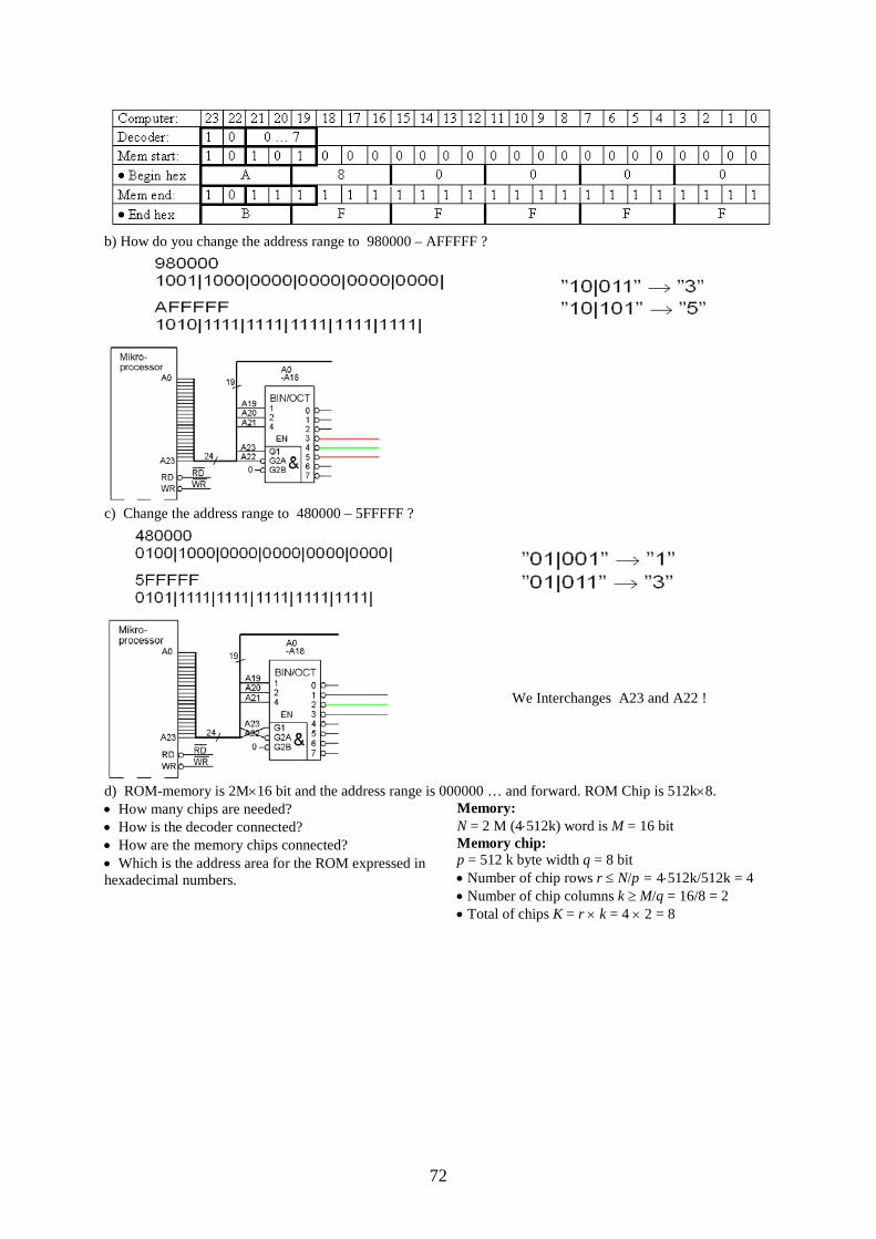
b) How do you change the address range to 980000 – AFFFFF ? c) How do you change the address range to 480000 – 5FFFFF ?
31
d) Typically a processor reads its first instruction from address 0 then there must be a read at that address. Assume that the ROM is 2M×16 bitar and that the address range is 000000 ... and beyond. ROM Chip is 512k×8. • How many chips are needed? • How should the decoder be connected? • How shall the memorychips be connected? • Specify address space of decoder outputs in hexadecimal. numbers.
e) Which address space becomes available for SRAM and IO circuits? 12.3 Peripherals, I/O, are often connected to a CPU as if they were memory chips (though with only a few "memory cells"). Eg. a real time clock chip - keeps track of the time and date. It is controlled/read from the 8 built-in 8-bit registers. a) Connect one eight registers memory-mapped peripheral device (I/O) to a CPU. The CPU has 16-bit data bus (we only use 8 bits), and a 24 bit address bus. Use a 3:8-decoder and if needed gates. The peripheral device must be connected so that the addresses are 0x200010 … 0x200017. (Compare with the previous task). b) What is incomplete decoding?

32
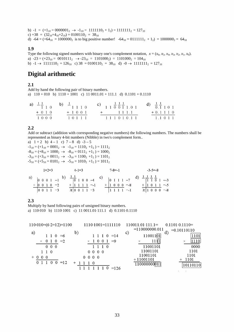
Solutions Number systems and codes 1.1 Enter the corresponding binary number (base 2) to the following decimal numbers (base 10). a) 910 = (1⋅23+0⋅22+ 0⋅21+1⋅20) = (8+1) = 10012 b) 1210 = (8+4) = 11002 c) 7110 = (64+7 = 64+4+2+1) = 10001112 d) 50310 = (512 – 9 = 511 – 8 ) = (1111111112 - 10002) = 1111101112 1.2 Convert the following binary number to decimal. a) 1011010012 = (28+26+25+23+20 = 256+64+32+8+1 ) = 36110 b) 110100.0102 = (25+24+22 + 2-2 = 32+16+4 + 0.25) = 52,2510 1.3 Convert the following binary numbers (base = 2) to the corresponding octal (base = 8) and hexadecimal (base = 16). a) 01 11012 = 1D16 = ( 011 1012) = 358 b) 1000 10112 = 8B16 = (010 001 0112) = 2138 c) 1 0011 01012 = 13516 = (100 110 1012) = 4658 d) 1101 1110 1001 00012 = DE9116 = (001 101 111 010 010 0012) = 1572218 e) 10 1001.0012 = 29.216 = (101 001 . 0012) = 51.18 1.4 Convert the following hexadecimal numbers (base = 16) to the corresponding octal (base = 8). a) 94D16 = (1001 0100 11012 = 100 101 001 1012) = 45158 b) 9E.7A16 = (1001 1110 . 0111 10102 = 010 011 110 . 011 110 1002) = 236.3648 1.5 Convert the octal (base = 8) number 45158 to the corresponding hexadecimal number (bas=16). 45158 = (100 101 001 1012 = 1001 01 00 11012) = 94D16 1.6 Write the hexadecimal (base = 16) number BAC16 in decimal form (bas=10). BAC16 = (11⋅162+10⋅161+12⋅160 = 11⋅256+10⋅16+12⋅1) = 298810 1.7 What characterizes Gray codes, and how can they be designed? Gray codes have the distance "one" between codewords. There is never more than one bit at a time that changes in the transitions from one codeword to the next. If one wants to construct an N-bit Gray code can do this from the code for the N-1 bits. First, follow the N-1 bit code with "0" as the bit N, then continue to the next half of the N-1 code again but with code words in reverse order, with "1" as bit N. This is a "mirrored binary code." This is how do you do 3-bit Gray code from 2-bit Gray code: 00 01 11 10 is a 2-bit Gray code. 000 001 011 010 is the code with "0" added as bit 3. 10 11 01 00 is the 2-bit code in reverse order. 110 111 101 100 is thereversed code with "1" added as bit 3. All together the 3-bit Gray code becomes: 000 001 011 010 110 111 101 100 This is not the only possible 3-bit Gray code, another possible code for the three bit are 000 010 011 001 101 111 110 100. (In general it is the "reflected binary code" you mean when you talk about Gray code). 1.8 Type the following signed numbers with binary two's complement notation, x = (x6, x5, x4, x3, x2, x1, x0). a) -23 = (+2310 = 00101112 → -2310 = 11010002 + 12 ) = 11010012 = 10510
33
b) -1 = (+110 = 00000012 → -110 = 11111102 + 12) = 11111112 = 12710 c) +38 = (3210+410+210) = 01001102 = 3810 d) -64 = (+6410 = 10000002 is to big positive number! -6410 = 01111112 + 12) = 10000002 = 6410 1.9 Type the following signed numbers with binary one's complement notation, x = (x6, x5, x4, x3, x2, x1, x0). a) -23 = (+2310 = 00101112 → -2310 = 11010002) = 11010002 = 10410 b) -1 → 11111102 = 12610 c) 38 = 01001102 = 3810 d) -0 → 11111112 = 12710
Digital arithmetic 2.1 Add by hand the following pair of binary numbers. a) 110 + 010 b) 1110 + 1001 c) 11 0011.01 + 111.1 d) 0.1101 + 0.1110
2.2 Add or subtract (addition with corresponding negative numbers) the following numbers. The numbers shall be represented as binary 4-bit numbers (Nibble) in two's complement form.. a) 1 + 2 b) 4 – 1 c) 7 – 8 d) -3 – 5 -110 = (+110 = 00012 → -110 = 11102 +12 ) = 11112 -810 = (+810 = 10002 → -810 = 01112 +12 ) = 10002 -310 = (+310 = 00112 → -310 = 11002 +12 ) = 11012 -510 = (+510 = 01012 → -510 = 10102 +12 ) = 10112
2.3 Multiply by hand following pairs of unsigned binary numbers. a) 110⋅010 b) 1110⋅1001 c) 11 0011.01⋅111.1 d) 0.1101⋅0.1110

34
2.4 Divide by hand following pairs of unsigned binary numbers. a) 110/010 b) 1110/1001 If the division is a integer division the answer of b) is the integer 1.
2.5 Assume that a 32-bit float is stored in a register: 40C8000016 what real decimal number is this? 32-bit floating point numbers are stored normalized as ”1.” One ”sign bit”, 8 bits for the 2-exponent (expressed as an exess-127), 23 bits for significand. Since all numbers are starting with "1" this “1” is not needed to be stored, it is implicitly understood. Exess-127 means that number 127 is added to all exponents, they are therefore always stored as positive numbers. This has the advantage that floating point numbers can be sized as if they were integers!
2.6 a)
b) The maximum quantization error occurs between 4 and 6 (or between -6 and -4). The error is (6-4)/2 = 1. c) Any representation of the number 0 does not exist, you can choose to use the smallest positive and smallest negative numbers as +0 and -0. This is done in the IEEE standard.
35
2.7
Float addition
Foat multiplckation (this is simpler than addition!)
36
Sets and Cubes Venn-diagram representation 3.1 Proof of the distributive law with the help of Venn diagrams.
)()( zxyxzyx +⋅+=⋅+
zyx ⋅+ )()( zxyx +⋅+
3.2 Proof of De Morgan's law using the Venn diagram.
yxyx +=⋅
yx ⋅ yx +
3.3 a) The minterms placement in a three variables Venn diagram.

37
b)
Venn diagram method clearly shows the boolean relationships, but are difficult to use for more than three variables. It is impractical to convert to a computer algorithm. 3.4 a) Represent the following function of three variables, as a 3-dimensional cube with Gray-coded corner.
012012012012012012 )6,4,3,2,0(),,( xxxxxxxxxxxxxxxmxxxf ++++== ∑ b) Use the cube to to simplify the function..
The cubic representation is hard to visualize for more than three dimensions, but the minimization method can be easily defined for any number of variables and dimensions, and then form the basis for computer algorithms.

38
Boolean algebra and gates 4.1 a) dacdadadcaf ⋅=+⋅⋅=⋅+⋅⋅= )1( b) abbabababaacaababacabaf =+⋅=⋅++⋅=⋅⋅+⋅⋅+⋅=⋅+⋅+⋅= )(0)( c)
1......)11(
}{)1(
=+=++⋅+⋅+⋅=
==++⋅+⋅=+⋅++=
aacaabab
consensuscababcbabaf
d) cacaccbcbbacabaacbacbaf ⋅=++⋅+=⋅⋅+⋅⋅⋅+⋅+⋅⋅=+⋅⋅⋅+= 000)()( e)
babababbabbabaabaabababa
babbbabaaabababaf
⋅=⋅+⋅=⋅⋅+⋅⋅+⋅⋅+⋅⋅=+⋅+⋅+⋅+
=+⋅⋅+⋅+⋅+⋅=+⋅+⋅+=
)()00(
)()()()()(
f)
cbcabac
bbacabbacabbacconsensusbbac
aabbacbababaccbacbacbaf
⋅+⋅=+⋅=
=++⋅⋅=++⋅⋅=⋅+⋅+⋅⋅==⋅+⋅⋅=
=+⋅+⋅⋅=⋅+⋅+⋅⋅=⋅⋅+⋅⋅+⋅⋅=
)(
))1(()()11(}{)1(
))(()(
g)
dcbayxyxxdcdcba
dcdcbadcdcbadcdbacbaf
⋅+⋅=+=+=⋅+⋅⋅⋅
=⋅++⋅⋅=⋅++⋅⋅=⋅+⋅⋅+⋅⋅=
}{
)()(
h) babaadeMorganbaaf +=++==⋅+= }{)( i)
accabaacbaadeMorgancbaaf =⋅+⋅⋅=+⋅⋅==+⋅+= )(}{ 4.2 Prove algebraically that the following relationships are valid.
a) 1)1( 121212323 =+++++ xxxxxxxxx LHS: 1...)1(... 1111 =++=+ xxxx
b) 1313123 )( xxxxxxx =++ LHS: 132131312313123 )1()( xxxxxxxxxxxxxxx =+=+=++
c) 31231212 )( xxxxxxxx +=++ LHS: 3123121231212 )( xxxxxxxxxxxxx +=+=++
d) 31231212 xxxxxxxx +=+++ LHS: 3123121231212 xxxxxxxxxxxxx +=++=+++ 4.3 Simplify the following three expressions as much as possible.
a) xzyxyzremoveconsensusyzxzyxyzxzxyxxzxyx +==++=+++=++ }{))((
b) 0000)())(( +++=+++=+++ yxyyxxyxyxyxxyyx
c) 1)1()1( =+=++ xxxyxx 4.4 Simplify the following expressions as much as possible.
cbcaaacbbbca
cbabcacbacbacbabcacbacbacbacba
cbacbacba
cbcbacbacbacbcbacbacba
+=+++=
=+++=++=++++++++
=++++++=
=+++++++=++++++
)()(
)()()(
))()((
))()(())()((
39
4.5
a) b) 4.6 simplify f(a,b) realized by the figure gates, as far as possible, and give the name of the function.
baabbaabbaabababbabaabba +=++=++=⊕⊕ ))(())(())(( It will be an XNOR function.
4.7
4.8 Indicate the logical expressions for A, B, C and D.
eaaeaaD
eaaeaaC
eaaeaaB
eaaeaaA
++==
++==
++==
++==
0101
0101
0101
0101
4.9 Simplify the complex expressions below as much as possible. a)
12221112
2121121221121212221
2112121212211212211212
2112122112122112
)()(
)00(
))(()00())((
)()(
xxxxxxxx
xxxxxxxxxxxxxxxxxxx
xxxxxxxxxxxxxxxxxxxxxx
xxxxxxxxxxxxxxxx
bababafunctionXOR
+=+++=
=+++=++=++++=
=++++++=+++=
=+++=⊕⊕
+=⊕−
b)
1212
121212121212121212 )()()()(
xxxx
xxxxxxxxxxxxxxxxxx
+=
=++=+++=+⊕
40
4.10 Show that
a) 121212 xxxxxx ⊕=⊕=⊕ This time we are proving the relationship with so-called "perfect induction." It involves directly inserting all four combinations of the two variables in the various expressions. If the expressions has the same truth table so they're equivalent. When the variables are few, this non algebraic method cold be used. x2 x1
2x 1x 12 xx ⊕ 12 xx ⊕ 12 xx ⊕ 0 0 1 1 1 1 1 0 1 1 0 0 0 0 1 0 0 1 0 0 0 1 1 0 0 1 1 1 b)
RHSLHSxxxxxxxxxxRHS
xxxxxxLHS
xxxx
=+=+=⊕
+=⊕
⊕=⊕
1212121212
121212
1212
:
:
4.11 The figure shows the international standard gate symbols. Name the gates and draw the corresponding American gate symbols.
AND OR NOT NAND NOR XOR XNOR
4.12 From text to Boolean expression.
)( 54200 xxxxu ⊕⊕⋅=
)( 25101 xxxxu ⊕⋅⊕=
54321054321025432102 )()( xxxxxxxxxxxxuxxxxxxu ⋅⋅⋅⋅+=++++⋅=⇒++++⋅=
41
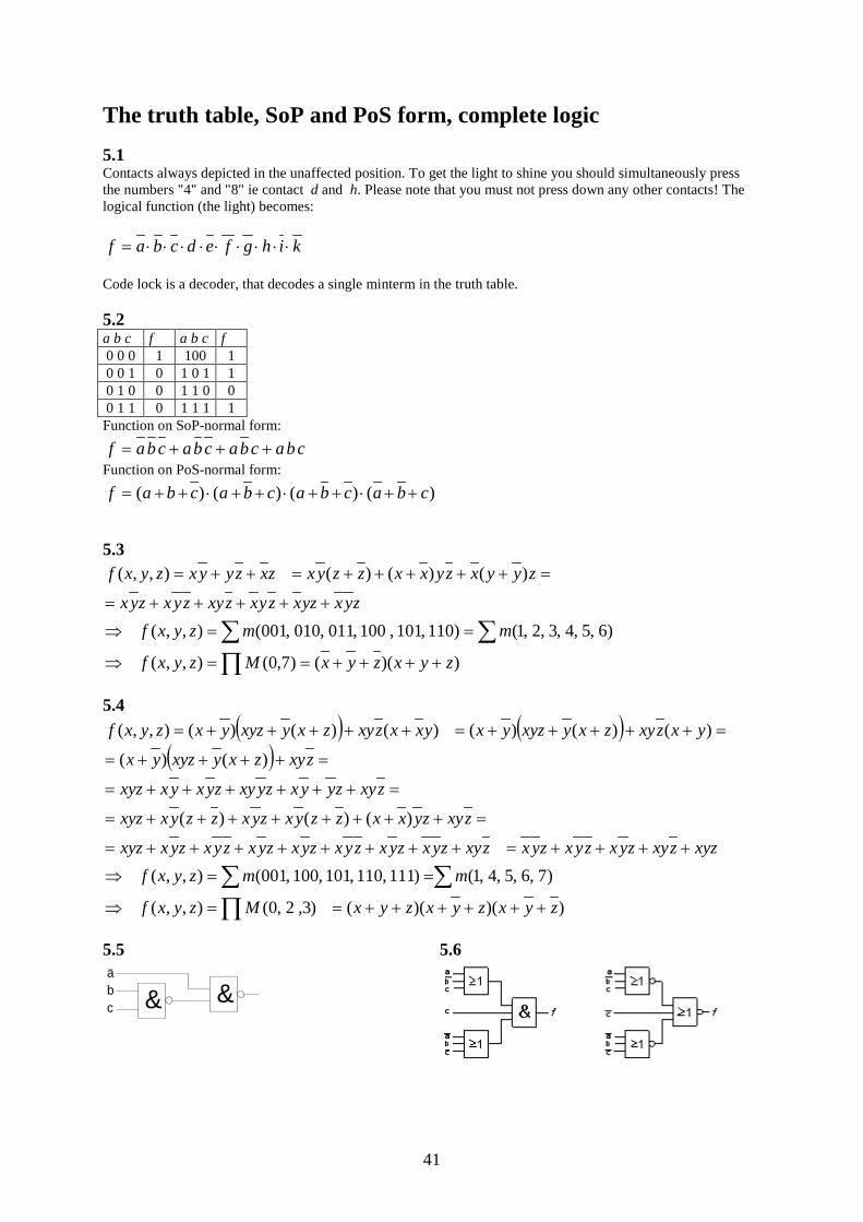
The truth table, SoP and PoS form, complete logic 5.1 Contacts always depicted in the unaffected position. To get the light to shine you should simultaneously press the numbers "4" and "8" ie contact d and h. Please note that you must not press down any other contacts! The logical function (the light) becomes:
kihgfedcbaf ⋅⋅⋅⋅⋅⋅⋅⋅⋅= Code lock is a decoder, that decodes a single minterm in the truth table. 5.2 a b c f a b c f 0 0 0 1 100 1 0 0 1 0 1 0 1 1 0 1 0 0 1 1 0 0 0 1 1 0 1 1 1 1 Function on SoP-normal form:
cbacbacbacbaf +++= Function on PoS-normal form:
)()()()( cbacbacbacbaf ++⋅++⋅++⋅++= 5.3
∏∑∑
++++==⇒
==⇒
+++++=
=+++++=++=
))(()7,0(),,(
)6,5,4,3,2,1()110,101,100,011,010,001(),,(
)()()(),,(
zyxzyxMzyxf
mmzyxfzyxyzxzyxzxyzyxzyx
zyyxzyxxzzyxzxzyyxzyxf
5.4
( ) ( )( )
))()(()3,2,0(),,(
)7,6,5,4,1()111,110,101,100,001(),,(
)()()(
)()(
)()()()()()(),,(
zyxzyxzyxMzyxf
mmzyxfxyzzxyzyxzyxzyxzxyzyxzyxzyxzyxzyxzyxzyxxyz
zxyzyxxzzyxzyxzzyxxyz
zxyzyyxzyxyzyxyxxyz
zxyzxyxyzyx
yxzxyzxyxyzyxyxxzxyzxyxyzyxzyxf
++++++==⇒
==⇒
++++=++++++++=
=++++++++=
=++++++=
=++++=
=+++++=+++++=
∏∑∑
5.5
&cba
&
5.6
42
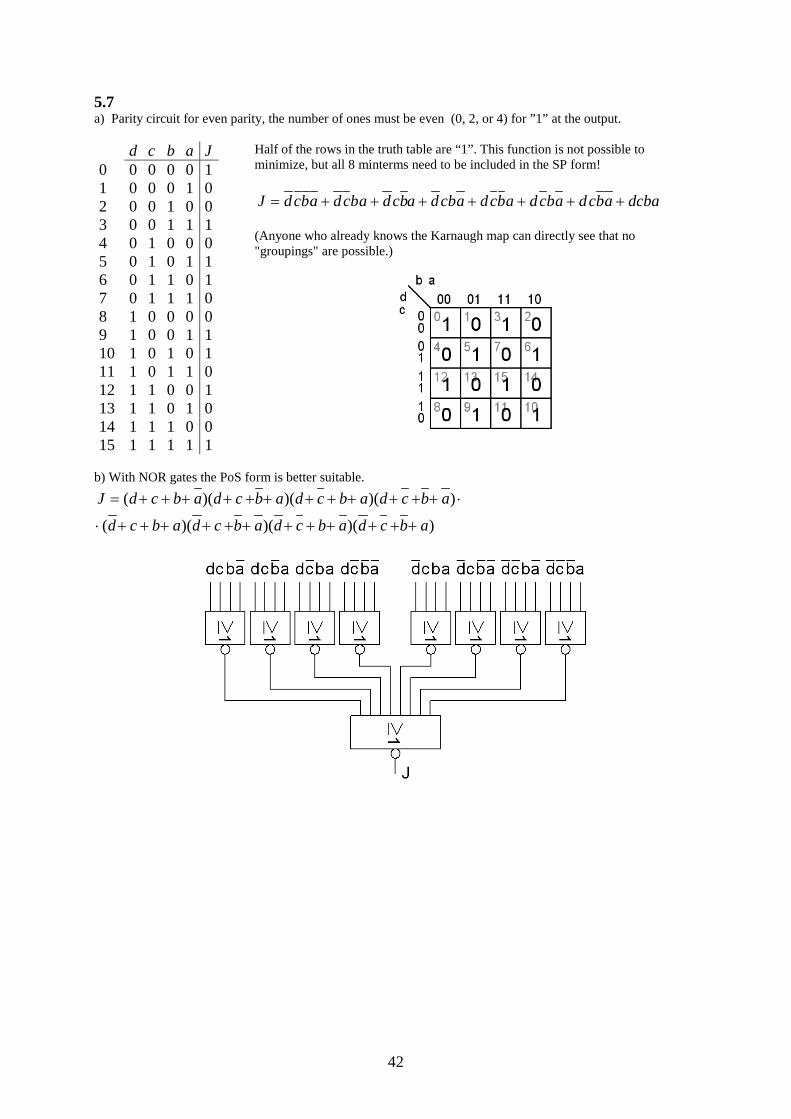
5.7 a) Parity circuit for even parity, the number of ones must be even (0, 2, or 4) for ”1” at the output. d c b a J 0 0 0 0 0 1 1 0 0 0 1 0 2 0 0 1 0 0 3 0 0 1 1 1 4 0 1 0 0 0 5 0 1 0 1 1 6 0 1 1 0 1 7 0 1 1 1 0 8 1 0 0 0 0 9 1 0 0 1 1 10 1 0 1 0 1 11 1 0 1 1 0 12 1 1 0 0 1 13 1 1 0 1 0 14 1 1 1 0 0 15 1 1 1 1 1
Half of the rows in the truth table are “1”. This function is not possible to minimize, but all 8 minterms need to be included in the SP form!
dcbaabcdabcdabcdabcdabcdabcdabcdJ +++++++= (Anyone who already knows the Karnaugh map can directly see that no "groupings" are possible.)
b) With NOR gates the PoS form is better suitable.
))()()((
))()()((
abcdabcdabcdabcd
abcdabcdabcdabcdJ
++++++++++++⋅
⋅++++++++++++=
43
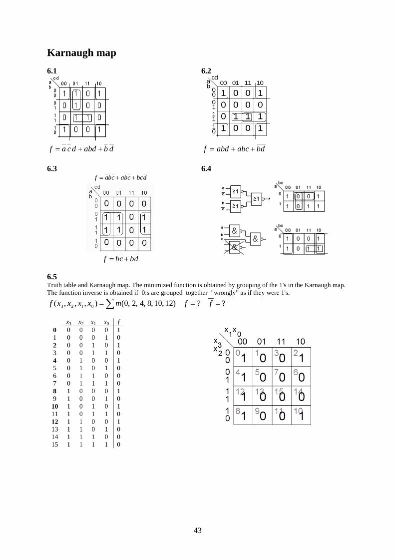
Karnaugh map 6.1 6.2
00ab
cd01 11 10
00
1110
01
00
000
0 0 001
1 1
1
1 1 1
dbabddcaf ++= dbabcabdf ++=
6.3 6.4
f abc abc bcd= + +
dbcbf +=
6.5 Truth table and Karnaugh map. The minimized function is obtained by grouping of the 1's in the Karnaugh map. The function inverse is obtained if 0:s are grouped together "wrongly” as if they were 1's.
??)12,10,8,4,2,0(),,,( 0123 === ∑ ffmxxxxf
x3 x2 x1 x0 f 0 0 0 0 0 1 1 0 0 0 1 0 2 0 0 1 0 1 3 0 0 1 1 0 4 0 1 0 0 1 5 0 1 0 1 0 6 0 1 1 0 0 7 0 1 1 1 0 8 1 0 0 0 1 9 1 0 0 1 0 10 1 0 1 0 1 11 1 0 1 1 0 12 1 1 0 0 1 13 1 1 0 1 0 14 1 1 1 0 0 15 1 1 1 1 0
44
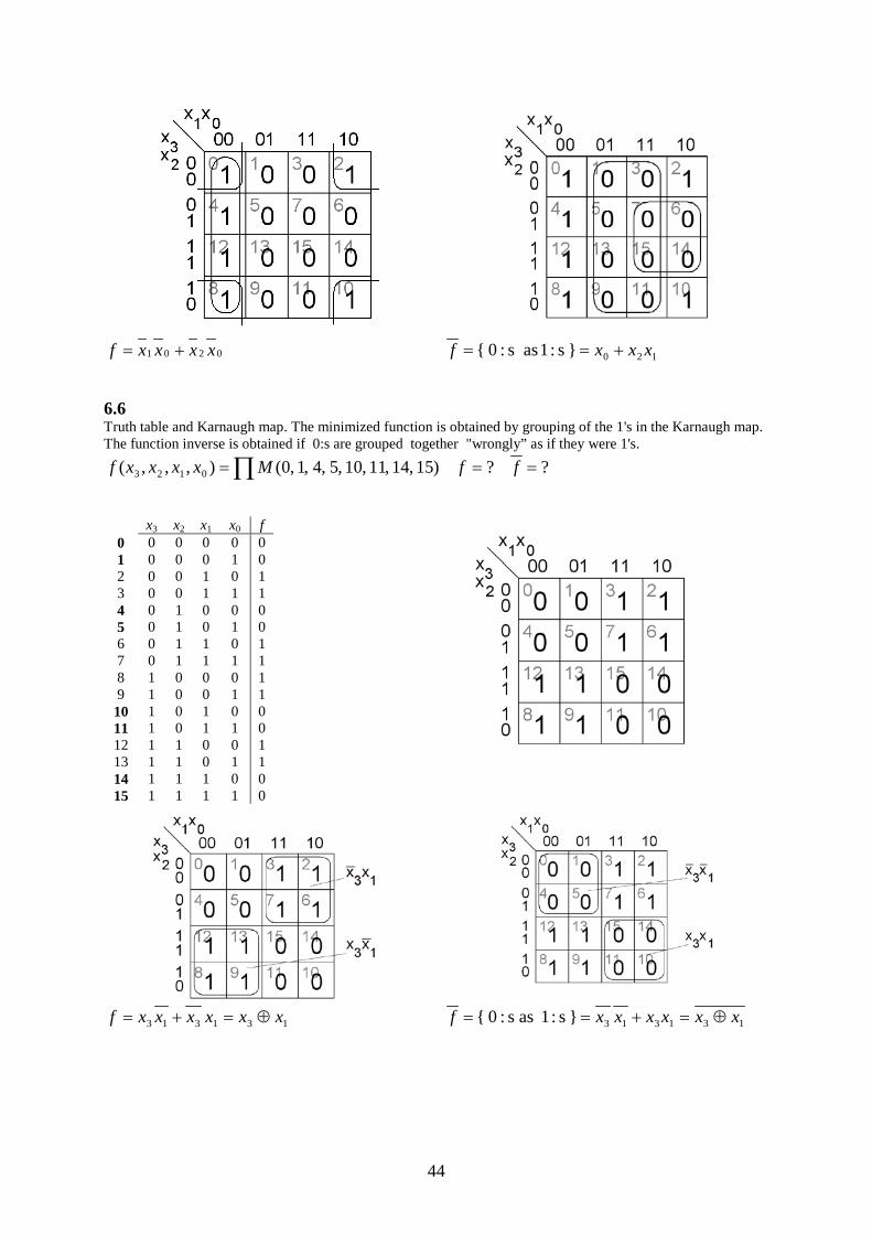
0201 xxxxf += 120}s:1 as s:0{ xxxf +== 6.6 Truth table and Karnaugh map. The minimized function is obtained by grouping of the 1's in the Karnaugh map. The function inverse is obtained if 0:s are grouped together "wrongly” as if they were 1's.
??)15,14,11,10,5,4,1,0(),,,( 0123 ===∏ ffMxxxxf
x3 x2 x1 x0 f 0 0 0 0 0 0 1 0 0 0 1 0 2 0 0 1 0 1 3 0 0 1 1 1 4 0 1 0 0 0 5 0 1 0 1 0 6 0 1 1 0 1 7 0 1 1 1 1 8 1 0 0 0 1 9 1 0 0 1 1 10 1 0 1 0 0 11 1 0 1 1 0 12 1 1 0 0 1 13 1 1 0 1 1 14 1 1 1 0 0 15 1 1 1 1 0
131313 xxxxxxf ⊕=+= 131313}s:1 ass:0{ xxxxxxf ⊕=+==
45
6.7 Truth table and Karnaugh map. The minimized function is obtained by grouping of the 1's in the Karnaugh map. The function inverse is obtained if 0:s are grouped together "wrongly” as if they were 1's.
??)14,13,12,10,9,8,7,6,4,3,2,0(),,,( 0123 === ∑ ffmxxxxf
x3 x2 x1 x0 f 0 0 0 0 0 1 1 0 0 0 1 0 2 0 0 1 0 1 3 0 0 1 1 1 4 0 1 0 0 1 5 0 1 0 1 0 6 0 1 1 0 1 7 0 1 1 1 1 8 1 0 0 0 1 9 1 0 0 1 1 10 1 0 1 0 1 11 1 0 1 1 0 12 1 1 0 0 1 13 1 1 0 1 1 14 1 1 1 0 1 15 1 1 1 1 0
13130 xxxxxf ++= 013013}s:1 ass:0{ xxxxxxf +==
46
6.8 ??)15,6()11,7,5,3(),,,( 0123 ==+= ∑ ffdmxxxxf
02301 xxxxxf += 13120 xxxxxf ++= 6.9
??)13,12,9,8,7,6,3,2()5,4,1(),,,( 0123 ==+= ∑ ffdmxxxxf
0112 xxxxf += 023 xxxf += or 1 2 0f x x x= +
47
6.10 Karnaugh map for five variables. The left diagram is for 4x and the right for 4x . If the same grouping can be
made in both diagrams then the variable 4x or 4x is omitted, otherwise it has to be included.
??),,,,( 01234 == ffxxxxxf
024023234 xxxxxxxxxf ++=
024240334 xxxxxxxxxf +++=
48
MOS-transistors and digital circuits 7.1
This is a CMOS-inverter. AY = . 7.2
This is a CMOS-NAND-gate. BAY ⋅= . 7.3
This is a CMOS-OR-gate. BAY += .
49
7.4 The circuit is an inverter with THREE-state output. When EN = 1 becomes the circled portion "plugged in" and the relationship between Y and A is then inverted, AY = . When EN = 0 becomes the circled portion "unplugged”. Output becomes disconnected and in a third state, exept ”1” and ”0” there is a state "disconnected". Since the output Y now is disconnected it is no longer affected by the input A.
THREE-state outputs are used to make it possible to connect many outputs to a single line (bus). Several circuits outputs can utilize a common input line, provided that only one of the circuits are active (EN = 1) at a time – the others has EN = 0 and are ”disconnected”. 7.5 CMOS-circuits cosists of two subcircuits that each other's inverses. The Pull-up-net, PUN, transfers ”1” to the output while the pull-down network transfers ”0”. If one analyzes the Pull-down network, one therefore get the function Y inverted.
BCABCABCAYBCAY )( +=⋅⋅=+⋅=⇒+⋅=
BCA )( + Pull-up-net shall have A and C in parallell (+) and then in series (⋅) with B. The use of PMOS-transistors inverts the variables A, B and C.
BCA )( +
50
Combinatorial circuits 8.1 X x2 x1 x0 U = X2 u5 u4 u3 u2 u1 u0 0 0 0 0 0 0 0 0 0 0 0 1 0 0 1 1 0 0 0 0 0 1 2 0 1 0 4 0 0 0 1 0 0 3 0 1 1 9 0 0 1 0 0 1 4 1 0 0 16 0 1 0 0 0 0 5 1 0 1 25 0 1 1 0 0 1 6 1 1 0 36 1 0 0 1 0 0 7 1 1 1 49 1 1 0 0 0 1 In the truth table we can see that u1 allways is equal to 0. u1 output can therefore be directly connected 0V (ground) so it will have the output constant 0. We can also see that u0 allways is equal to x0. u0 output can therefore be directly connected to the x0 input. The other expressions are obtained by using their Karnaugh maps.
8.2 X x3 x2 x1 x0 U u2 u1 u0
0 0 0 0 0 0 0 0 0 1 0 0 0 1 1 0 0 1 3 0 0 1 1 2 0 1 0 7 0 1 1 1 3 0 1 1 15 1 1 1 1 4 1 0 0 In the truth table we can see that u2 and x3 are equal why u2 directly can be connected to x3. u2 = x3. The other expressions are obtained by using their Karnaugh maps.
51
Gate circuits:
8.3 Truth table
r5 r4 r3 r2 r1 y4 y2 y1 1 - - - - 1 0 1 0 1 - - - 1 0 0 0 0 1 - - 0 1 1 0 0 0 1 - 0 1 0 0 0 0 0 1 0 0 1 0 0 0 0 0 1 1 1
52
8.4 7 4 2 1 8 4 2 1 x7 x4 x2 x1 y8 y4 y2 y1 (0) 0 0 0 0 0 0 0 0 0 (1) 0 0 0 1 1 0 0 0 1 (2) 0 0 1 0 2 0 0 1 0 (3) 0 0 1 1 3 0 0 1 1 (4) 0 1 0 0 4 0 1 0 0 (5) 0 1 0 1 5 0 1 0 1 (6) 0 1 1 0 6 0 1 1 0 (8) 1 0 0 0 7 0 1 1 1 (9) 1 0 0 1 8 1 0 0 0 (10) 1 0 1 0 9 1 0 0 1
12727171
127272
12744
17278
xxxxxxxy
xxxxxy
xxxxy
xxxxy
++=
+=
+=
+=
Two of the AND-gates can be common to the y8,y1 and y8,y2,y1 -circuits.
8.5
53
8.6 A 4-1 multiplexer used as function generator for the OR-function.
8.7 a b c M 0 0 0 0 0 1 0 0 1 0 2 0 1 0 0
3 0 1 1 1 cba 4 1 0 0 0
5 1 0 1 1 cba
6 1 1 0 1 cba 7 1 1 1 1 cba
abacbcM ++=
)()()()( cbacbacbcbcbacbacbacbacbacbaM ++=+++=+++=
cbccbbbcbccbcbccbcbbcbh
bccbbg
cbhbcgcbacbaM
+=+++=++=++=+=
=+=
+==++=
)()()()1()(
)()0(
)()(
54
8.8 In order to make a full adder we need to use the the upper MUX to the sum function, and the bottom MUX, which is connected to COUT , is used for the Carry-function. In stead of x0 we choose CIN. In order for the upper MUX to be connected to the logic element output the output mux must be controlled with 0 instead of with x3.
x2 x1 x0 A B CIN ∑ COUT 0 0 0 0 0 0 0 1 1 0 0 1 0 1 0 0 1 1 0 1 1 0 0 1 0 1 0 1 0 1 1 1 0 0 1 1 1 1 1 1
8.9
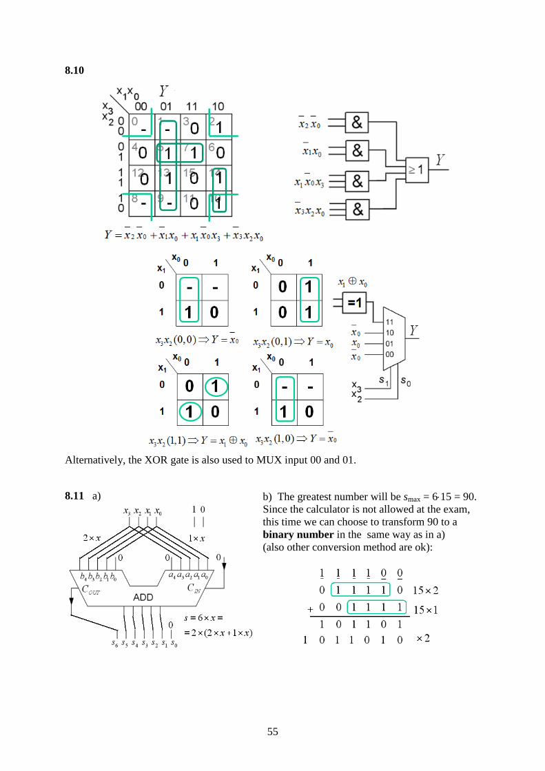
55
8.10
Alternatively, the XOR gate is also used to MUX input 00 and 01. 8.11 a)
b) The greatest number will be smax = 6⋅15 = 90. Since the calculator is not allowed at the exam, this time we can choose to transform 90 to a binary number in the same way as in a) (also other conversion method are ok):
56
8.12
57
Sequential circuits, latches and clocked flip-flops 9.1 The figure shows a SR-latch, but at the end of the input-sequence the “forbidden” input combination S = 1, R = 1 will occur. The outputs Utgångarna will not be each others inverses for this combination. For NOR-gates is 1 a locking input signal, therefore
0=Q as long as S is left at 1.
9.2
9.3
9.4
9.5
JK-flip-flop can be used as T-flip-flop or as D-flip-flop. ( When flip-flops are connected to each other there are usually the inverted outputs available, you will then not require the inverter to make the JK flip flop to D flip-flop. )
58
9.6
[ ] MHz20ns)3020(
111=
+=
+==
+=
spd
spd
ttTf
ttT
9.7
9.8 a) The clock period is determined by the longest path, the one with the XOR-gate. TCP > tpdQ + tsu + tpdXOR = 3+4+5 = 12 ns.
b) Hold time is the time the data input must be stable after the clock
edge. The flip-flop that has its D-input directly connected to the 0Q will get it’s D-input changed first, directly after tpdQ = 3 ns. th < 3 ns.

59
Sequential circuits 10.1 From the circuit diagram one can be derive the following expressions:
010
01
01
qqxq
qxqqq
⋅+=
⋅=+
+
No output decoder exists the flip-flop state is directly used as output. Moore model is to be used.
10.2 From the circuit diagram one can be derive the following expressions:
10010
10011
00
)(
)(
qqxxqqq
qqxxqqq
qxqxU
+⋅=⋅⋅=
⋅+=⋅⋅=
+=⋅=
+
+
Since U depends directly of x must Mealy model be used.
60
10.3 From the circuit diagram one can be derive the following expressions:
xqqqqxq
qqqqU
+=⋅⋅=
=
+=⋅=
+
+
01100
01
1010
Since U only depends on the state and is is independent of x must Moore model be used.
(10.4)
• Stopping condition: Z3 • Loss condition: Z7 • Isolated states: Z2
10.5
Z0Z:CPi
Z0 Z1 Z4 Z6 Z0 Z0 Z1 Z2 Z3
10.6 From state diagram to coded state table.
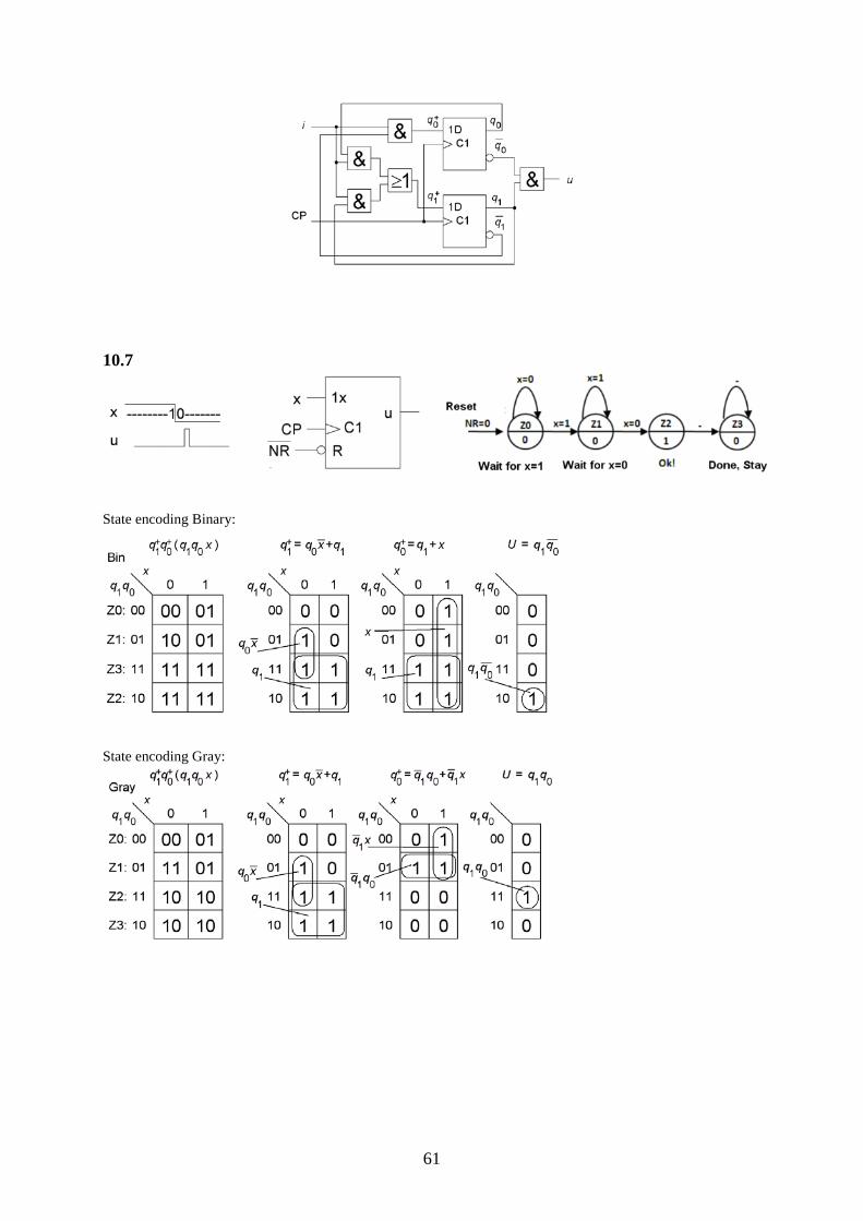
61
10.7
State encoding Binary:
State encoding Gray:
62
State encoding One hot:
This is how to do reset to ”00” with CLR inputs for the Bin/Gray state encoding, and to ”0001” with PRE/CLR inputs for the ”one hot” state encoding.
63
10.8 Six state requires three flip-flops. There are 8 states in total, two states which are not included in the sequence. To be on the safe side we specify what should happen with these states, so that the counter will not get “stuck” at Z0 or Z7.
Equations with EN (EN=0 → next state same) : Equations with S6 (S6 = 1 → next state is 110) :
)()()'(
)()()'(
)()()'(
000
111
222
qENqENq
qENqENq
qENqENq
⋅+⋅=
⋅+⋅=
⋅+⋅=
++
++
++
6)'(')'(
6)'(')'(
6)'(')'(
00
11
22
Sqq
SqqSqq
⋅=
+=
+=
++
++
++
10.9

64
10.10
65
10.11
Groups with same output: ),)(,,,(1 edfcbaP =
Examine next states:
),,,(),,,(),,,(),,,(
),,,(),,,(),(),(
),,,(),(),,,(),(
10
10
10
10
10
10
fcbaefcbaefcbadfcbad
fcbaffcbafedcedc
fcbabedbfcbaaeda
ii
ii
ii
ii
ii
ii
→→→→
→→→→→→→→
==
==
==
==
==
==
Groups with same subsequent state output:
23
2 ),)()()(,(PP
edfcbaP==
10.12
66
Asynchronous sequential circuits 11.1
ACABCBGHazardfreeABCBG ++=+= }{ 11.2 To the left is a SR-latch made by two gates with feedback. To the right the circuit is drawn as a Moore-compatible statemachine. Moore-machine.
QRRSQSRQSRQSRQ +=+⋅=+⋅=++=+ )()( When dealing with asynchronous statemachines the coded state table is used to be named excitation table.
For each input (column), there must be at least one state where Q = Q+. Such conditions are stable and they are usually marked by a circle. The state diagram follows from the exitation table. The state table is named flow table when working with asynchronous state machines..
11.3

67
11.4
• At positive edge ↑ C changes from 0 to 1 and when C=1 the MUX connects the upper flip-flop q0 to the output. • At negative edge ↓ C changes from 1 to 0 and C=0 the MUX connects the lower flip-flop q1 to the output. The result is a D-flip-flop that reacts on both edges of the clock. 11.5 There are four input combinations (CD) and two output combinations (Q). A total of 8 possible states (CDQ).: Possible input/output combinations Present state Next state Comment State tag CDO (CDO)+ (CDO)+
A 000 010 100 Output O gets D input value when C changes value B 001 011 100 C 010 000 111 No change of O when D changes value D 011 001 111 E 100 000 110 F 101 000 111 G 110 011 100 H 111 011 101
Flow table (stabile states marked in bold font) Present state
Next State Output (CD)
00 01 11 10 A A C - E 0 B B D - E 1 C A C H - 0 D B D H - 1 E A - G E 0 F A - H F 1 G - D G E 0 H - D H F 1
We see immediately that no minimization may be done by state equivalence classes, because all eight states have different outputs where they have stable states, and where they have do not cares in the table. Merger-diagram:
68
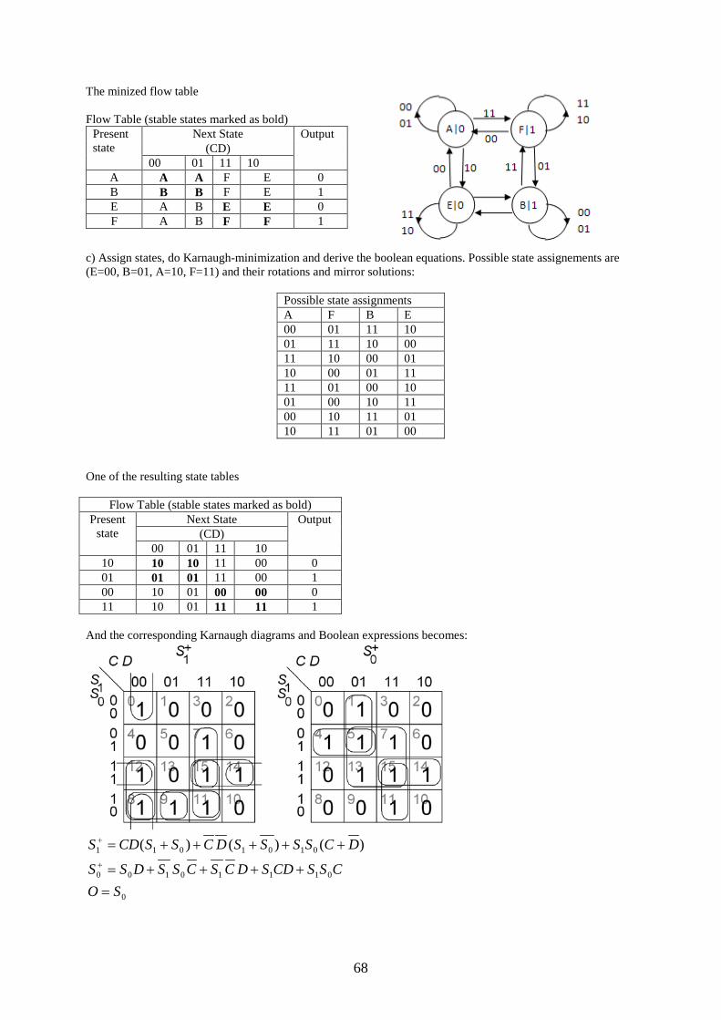
The minized flow table Flow Table (stable states marked as bold)
Present state
Next State Output (CD)
00 01 11 10 A A A F E 0 B B B F E 1 E A B E E 0 F A B F F 1
c) Assign states, do Karnaugh-minimization and derive the boolean equations. Possible state assignements are (E=00, B=01, A=10, F=11) and their rotations and mirror solutions:
Possible state assignments A F B E 00 01 11 10 01 11 10 00 11 10 00 01 10 00 01 11 11 01 00 10 01 00 10 11 00 10 11 01 10 11 01 00
One of the resulting state tables
Flow Table (stable states marked as bold) Present
state Next State Output
(CD) 00 01 11 10
10 10 10 11 00 0 01 01 01 11 00 1 00 10 01 00 00 0 11 10 01 11 11 1
And the corresponding Karnaugh diagrams and Boolean expressions becomes:
0
01110100
0101011 )()()(
SOCSSCDSDCSCSSDSS
DCSSSSDCSSCDS
=++++=
+++++=+
+

69
11.6 a) Derive the Boolean expressions for the state variables. Answer:
CYCIYIYYY
CYCYYYY
10011
10100
)()( +⊕+⊕=
++=+
+
b Derive the exitations table. Which function (dashed) are in the inner loops. The two inner loops are hazard-free MUX:es!
Derive the flow table, assign symbolic states and drav FSM.
Identify the function of the asynchronous circuit. Which flip-flop is it? • Positive edge-triggered T-flip-flop.

70
11.7
Folow the timing diagram and create a new state for every combination that has not been before. In state a we ”waits” for the startedge (b), then input 10 is impossible (marked with *). The Protocol prohibits change of data SDA when SCL is high. Therefore input 01 is impossible in state e (marked with *). This gives us two extra don’t care positions in the table. You can directly see which states that can be merged.
As state code assignement the Gray-code can be used. a 00, bc 01, de 11, and x 10. x can be used as don’t care exept from 10.
The groups are forming contiguous areas in Karnaughdiagram and therefore hazard free (if the networks have two levels). Realising with optional gates.
71
Address decoding of memories and I/O circuits 12.1 A dynamic RAM-memory consits of some 256Mbit memory chips organised as 32 M×8. a) How many chips are needed for 256M×64? Memory N = 256M M = 64 bit. Chip p = 32M q = 8 bit. Number of columns k = M/q = 64/8 = 8. Number of rows r = N/p = 256M/32M = 8. Total number of chips K = r × k = 8×8 = 64. b) How many memory chips are needed for 512M×72? (what can be the reson for the unusual widh ”72” of the memory?) Memory N = 512M M = 72 bit. Chip p = 32M q = 8 bit. Number of columns k = M/q = 72/8 = 9. Number of rows r = N/p = 512M/32M = 16. Total number of chips K = r × k = 9 ×1 6 = 144. The unusual “width” 72 (= 64 + 8). The 8 extra bits are used for correcting single errors and detecting double errors. (Not shown in this course). 12.2 A certain 16 bit processor can address 24 bits. Memory Space is divided between ROM, SRAM and IO circuits. Address decoding is done using a 3:8-decoder. a) How large is the RAM in the figure? What is the address range expressed in hexadecimal numbers?
• Memory chip: p = 512k q = 8 bitar • Memory: r = 3 k = 2 K = 2 × 3 = 6 M = k × q = 2 × 8 = 16 bitar N = p × r = 512k × 3 = 1,5M Address range:
72
b) How do you change the address range to 980000 – AFFFFF ?
c) Change the address range to 480000 – 5FFFFF ?
We Interchanges A23 and A22 !
d) ROM-memory is 2M×16 bit and the address range is 000000 … and forward. ROM Chip is 512k×8. • How many chips are needed? • How is the decoder connected? • How are the memory chips connected? • Which is the address area for the ROM expressed in hexadecimal numbers.
Memory: N = 2 M (4⋅512k) word is M = 16 bit Memory chip: p = 512 k byte width q = 8 bit • Number of chip rows r ≤ N/p = 4⋅512k/512k = 4 • Number of chip columns k ≥ M/q = 16/8 = 2 • Total of chips K = r × k = 4 × 2 = 8

73
00ab|cmmm|mmmm|mmmm|mmmm|mmmm 0000|0000|0|0|0|0 - 0000|0111|F|F|F|F 000000-07FFFF 0000|1000|0|0|0|0 - 0000|1111|F|F|F|F 080000-0FFFFF 0001|0000|0|0|0|0 - 0001|0111|F|F|F|F 100000-17FFFF 0001|1000|0|0|0|0 - 0001|1111|F|F|F|F 180000-1FFFFF
Total ROM 000000 – 1FFFFF e) Which address range is free for SRAM and IO-circuits? 00ab|cmmm|mmmm|mmmm|mmmm|mmmm 0010|0000|0|0|0|0 - 0010|0111|F|F|F|F 200000-27FFFF 0010|1000|0|0|0|0 - 0010|1111|F|F|F|F 280000-2FFFFF 0011|0000|0|0|0|0 - 0011|0111|F|F|F|F 300000-37FFFF 0011|1000|0|0|0|0 - 0011|1111|F|F|F|F 380000-3FFFFF
Possible SRAM+I/O addresses 200000 – 3FFFFF 12.3 a) Connect a 8 register memory-mapped peripheral device (I/O) to a CPU. The CPU has 16-bit data bus (only 8 bits are used by the chip), and a 24 bit address bus. Use a 3:8-decoder and if needed gates. The peripheral device must be connected so that it has register addresses 0x200010 … 0x200017. 0x200010 = 0010|0.000|0000|0000|0001|0.000 0x200011 = 0010|0.000|0000|0000|0001|0.001 0x200012 = 0010|0.000|0000|0000|0001|0.010 0x200013 = 0010|0.000|0000|0000|0001|0.011
I/O addresses, 200000 – 27FFFF is to be found, acording to the previous exercise, at the 3:8-decoder output ”4”. It decodes A23... A19, the peripheral itself decodes A2 ... A0,

74
0x200014 = 0010|0.000|0000|0000|0001|0.100 0x200015 = 0010|0.000|0000|0000|0001|0.101 0x200016 = 0010|0.000|0000|0000|0001|0.110 0x200017 = 0010|0.000|0000|0000|0001|0.111
the rest we have to decode with an and-gate
b) what is meant by incomplete decoding? For full decoding, we used a &-gate with 17 inputs! Sometimes you make a partial decoding. Then you omits address signals and thus can use a gate with fewer inputs I/O device addressing is ambiguous, it can be addressed with many different addresses, but the one who writes the program code determines which addresses to use. The main thing is to ensure that the I/O device addresses do not collide with any other device addresses.

75