Embed Size (px)
Citation preview

Disclaimer: This course was prepared, in its entirety, by Adam Teman. Many materials were copied from sources freely available on the internet. When possible, these sources have been cited;
however, some references may have been cited incorrectly or overlooked. If you feel that a picture, graph, or code example has been copied from you and either needs to be cited or removed,
please feel free to email [email protected] and I will address this as soon as possible.
Prof. Adam Teman
25 May 2021
Digital Integrated Circuits(83-313)
Lecture 9:
Memory Peripherals

May 25, 2021© Adam Teman,
Lecture Content
2

Memory Peripherals Overview
3

May 25, 2021© Adam Teman,
Memory Architecture
4
Memory Size: W Words of C bits
=W x C bits
Address bus: A bits
→W=2A
Number of Words in a Row: 2M
Multiplexing Factor: M
Number of Rows: 2A-M
Number of Columns: C x 2M
Row Decoder: A-M → 2A-M
Column Decoder: M → 2M
Word Line
Bit Line
Storage Cell
Ro
w D
eco
der
Sense Amplifiers /Drivers
Column Decoder
AD
DA
-1 :
AD
DM
ADDM-1 :
ADD0
C×2M
Input/Output(C bits)

May 25, 2021© Adam Teman,
Synchronous SRAM Interface
• A typical on-chip synchronous SRAM features:
• Single-cycle write/read latency
• Byte write mask
• Active low Write Enable (i.e., WEN=1 → Read Enable)
• The timing diagram can be viewed, as follows:
5
A[m-1:0]
D[n-1:0]
WEN[p-1:0]
CEN
Q[n-1:0]
2mxn SRAM
CLK
A
CLK
D
WE
Q
A0 A1 A2 A3
D0 D1
D2 D3
(1) Rising edge of the clock results
in WRITE, when WE is low.
(2) Rising edge of the clock results
in READ, when WE is high.
Valid data appears on the
output after a delay.

May 25, 2021© Adam Teman,
Memory Timing: Definitions
6
Simple Definitions
Real Datasheet
Example
Source: CMU, ECE548
Write Cycle Read Cycle

May 25, 2021© Adam Teman,
Major Peripheral Circuits
• Row Decoder
• Column Multiplexer
• Sense Amplifier
• Write Driver
• Precharge Circuit
7
Word Line
Bit Line
Storage Cell
Ro
w D
eco
der
Sense Amplifiers /Drivers
Column Decoder
AW
-1 :
AM
AM-1 : A0
C×2M
Input/Output(C bits)

Row Decoder Design
8

May 25, 2021© Adam Teman,
Row Decoders
• A Decoder reduces the number of select signals by log2.
• Number of Rows: W
• Number of Row Address Bits: A=log2W
9 Row Decoder Column Mux Precharge Sense Amp
Ro
w D
eco
der
AD
DA
-1 :
AD
D0
Word 0
Word 1
Word 2
Word W-2
Word W-1

May 25, 2021© Adam Teman,
Row Decoders
• Standard Decoder Design:
• Each output row is driven by an AND gate with k=log2N inputs.
• Each gate has a unique combination of address inputs
(or their inverted values).
• For example, an 8-bit row address has 256 8-input AND gates, such as:
• NOR Decoder:
• DeMorgan will provide us with a NOR Decoder.
• In the previous example, we’ll get 256 8-input NOR gates:
10
0 7 6 5 4 3 2 1 0WL A A A A A A A A= 255 7 6 5 4 3 2 1 0WL A A A A A A A A=
0 7 6 5 4 3 2 1 0WL A A A A A A A A= + + + + + + +
255 7 6 5 4 3 2 1 0WL A A A A A A A A= + + + + + + +
Row Decoder Column Mux Precharge Sense Amp

May 25, 2021© Adam Teman,
How should we build it?
• Let’s build a row decoder for a 256x256 SRAM Array.
• We need 256 8-input AND Gates.
• Each gate drives 256 bitcells
• We have various options:
• Which one is best?
11 Row Decoder Column Mux Precharge Sense Amp
WL0
WL1
WL255

May 25, 2021© Adam Teman,
Reminder: Logical Effort
12
( ),pd i pINV i it t p EF= +
, 1
,
i in i
i i i i
in i
b CEF LE f LE
C
+ =
,1
Li i
in
CPE F LE B LE b
C= =
N Nopt i iEF PE F LE b= =
log logopt optopt EF EFN PE F LE B= =
( ) ( )N
pd pINV i i pINV it t p EF t p N PE = + = +
Row Decoder Column Mux Precharge Sense Amp

May 25, 2021© Adam Teman,
Problem Setup
• For LE calculation we need to start with:
• Output Load (CL)
• Input Capacitance (Cin)
• Branching (B)
• What is the Load Capacitance?
• 256 bitcells on each Word Line
• Let’s ignore the wire for now…
• What is the Input Capacitance?
• Let’s assume our address drivers
can drive a bit more than a bitcell, so:
13
256WL Cell WireC C C= +
, _ 4in addr driver CellC C= Row Decoder Column Mux Precharge Sense Amp

May 25, 2021© Adam Teman,
Problem Setup
• What is the Branching Effort?
• Lets take another look
at the Boolean expressions:
• We see that half of the signals use Ai and half use Ai!
• So each address driver drives 128 8-input AND gates,
but only one is on the selected WL path.
14
0 7 6 5 4 3 2 1 0
255 7 6 5 4 3 2 1 0
WL A A A A A A A A
WL A A A A A A A A
=
=
_
; 127
127128
on path nand off path nand
on path off path nand nandadd driver
on path nand
C C C C
C C C CB
C C
= =
+ + = = =
Row Decoder Column Mux Precharge Sense Amp

May 25, 2021© Adam Teman,
Number of Stages
• Altogether the path effort is:
• The best case logical effort is
• So the minimum number of
stages for optimal delay is:
• That’s a lot of stages!
15
13
256128
4
8 2
WL Celli
address Cell
C CPE LE B F LE b LE
C C
LE k LE
= = =
= =
1LE =
13
13
3.6
2
log 2 7opt
PE
N
=
= =
Row Decoder Column Mux Precharge Sense Amp

May 25, 2021© Adam Teman,
So which implementation should we use?
• The one with the minimum Logical Effort:
16
( )10 3 1
10 3;
8 1 9
LE
p
=
=
= + =
( )2 5 3
10 3
4 2 6
LE
p
=
=
= + =
( ) ( ) ( )4 3 5 3 4 3 1
80 27;
2 2 2 1 7
LE
p
=
=
= + + + =
( )3
4 3
2.37;
2 3 1 3 9
LE
p
=
=
= + =
Row Decoder Column Mux Precharge Sense Amp

May 25, 2021© Adam Teman,
New optimal number of Stages
• So now we can calculate the actual path effort:
• We could add another inverter or two
to get closer to the optimal number of stages…
17
13
3.6
2.37 2 19.418
log 7.7
i i
opt
PE F b LE
k
N PE
= =
= =
= =
Row Decoder Column Mux Precharge Sense Amp

May 25, 2021© Adam Teman,
Implementation Problems
• Address Line Capacitance:
• Our assumption was that Cin,addr_driver=4Ccell.
• But each address drives 128 gates
• That’s a really long wire with high capacitance.
• This means that we will need to buffer the address lines• This will probably ruin our whole analysis...
• Bit-cell Pitch:
• Each signal drives one row of bitcells.
• How will we fit 8 address signals into this pitch?
18 Row Decoder Column Mux Precharge Sense Amp

May 25, 2021© Adam Teman,
Predecoding - Concept
• Solution:
• Let’s look at two decoder paths: WL254, WL255
• We see that there are many “shared” gates.
• So why not share them?
• For instance, we can use the purple output for both gates…
19 Row Decoder Column Mux Precharge Sense Amp
WL255
A0
A1
A2
A3
A4
A5
A6
A7
WL254
A0
A1
A2
A3
A4
A5
A6
A7A6
A7
A0
A1
A2
A3
A4
A5
A6
A7
A0
A1
A2
A3
A4
A5

May 25, 2021© Adam Teman,
Predecoding - Method
• How do we do this?
• If we look at the final Boolean expression,
it has combinations of groups of inputs.
• By grouping together a few inputs,
we actually create a small decoder.
• Then we just AND the outputs of all the
“pre” decoders.
• For example: Two 4:16 predecoders
20
( ) ( )0 1 2 3 4 5 6 7
0 0 0 255 15 15 254 14 15
, , , ; , , , ;
; ; ;
D dec A A A A E dec A A A A
WL D E WL D E WL D E
= =
= = =
Row Decoder Column Mux Precharge Sense Amp
4 →16
E
A4A5A6A7
4 →16
D
A0A1A2A3

May 25, 2021© Adam Teman,
Predecoding - Example
• Let’s look at our example:
• What is our new branching effort?
• As before, each address drives half the lines of the small decoder.
• Each predecoder output drives 256/16 post-decoder gates.
• Altogether, the branching effort is:
• Same as before!
21
( )
( )0 1 2 3
4 5 6 7
, , ,
, , ,
D dec A A A A
E dec A A A A
=
=
0 0 0
255 15 15
254 15 14
WL D E
WL D E
WL D E
=
=
=
_16 256 128
2 16addr driver predecoderB b b= = =
Row Decoder Column Mux Precharge Sense Amp

May 25, 2021© Adam Teman,
Predecoding - Solution
• Why is this a better solution?
• Each Address driver is only driving eight gates
• less capacitance.
• We saved a ton of area by “sharing” gates.
• We can “Pitch Fit” 2-input NAND gates.
22 Row Decoder Column Mux Precharge Sense Amp

May 25, 2021© Adam Teman,
Another Predecoding Example
• We can try using four 2-input predecoders:
• This will require us to use 256 4-input NAND gates.
23 Row Decoder Column Mux Precharge Sense Amp

May 25, 2021© Adam Teman,
How do we choose a configuration?• Pitch Fitting: 2-input NANDs vs. 4-input NAND.
• Switching Capacitance: How many wires switch at each transition?
• Stages Before the large cap: Distribution of the load along the delay.
• Conclusion: Usually do as much predecoding as possible!
24
2→ 4 2→ 4 2→ 4 2→ 4
A0A1 A2A3 A4A5 A6A7
WL0
WL127
WL1
4 4 4 4
WL0
WL127
WL1
4 → 16
A0A1A2A3
16
4 → 16
A4A5A6A7
16
Row Decoder Column Mux Precharge Sense Amp

May 25, 2021© Adam Teman,
Alternative Solution: Dynamic Decoders
25 Row Decoder Column Mux Precharge Sense Amp
2-input NOR decoder
PC
VD
D
GN
D
GN
D
A0
A0
A1
A1
WL0
WL1
WL2
WL3
2-input NAND decoder
WL3
WL2
WL1
WL0
A0
A0
A1
A1

Column Multiplexer
26

May 25, 2021© Adam Teman,
Column Multiplexer
• First option – PTL Mux with decoder
• Fast – only 1 transistor in signal path.
• Large transistor Count
27
A0A1
B0 B1 B2 B3
Y
Row Decoder Column Mux Precharge Sense Amp

May 25, 2021© Adam Teman,
4 to 1 tree decoder
• Second option – Tree Decoder
• For 2k:1 Mux, it uses k series transistors.
• Delay increases quadratically
• No external decode logic → big area reduction.
28 Row Decoder Column Mux Precharge Sense Amp
May 25, 2021© Adam Teman,
Combining the Two
29 Row Decoder Column Mux Precharge Sense Amp

Precharge and Sense Amp
30

May 25, 2021© Adam Teman,
Precharge Circuitry
• Precharge bitlines high before reads
• Equalize bitlines to minimize voltage difference when using sense amplifiers
31
bit bit_b
bit bit_b
Row Decoder Column Mux Precharge Sense Amp
May 25, 2021© Adam Teman,
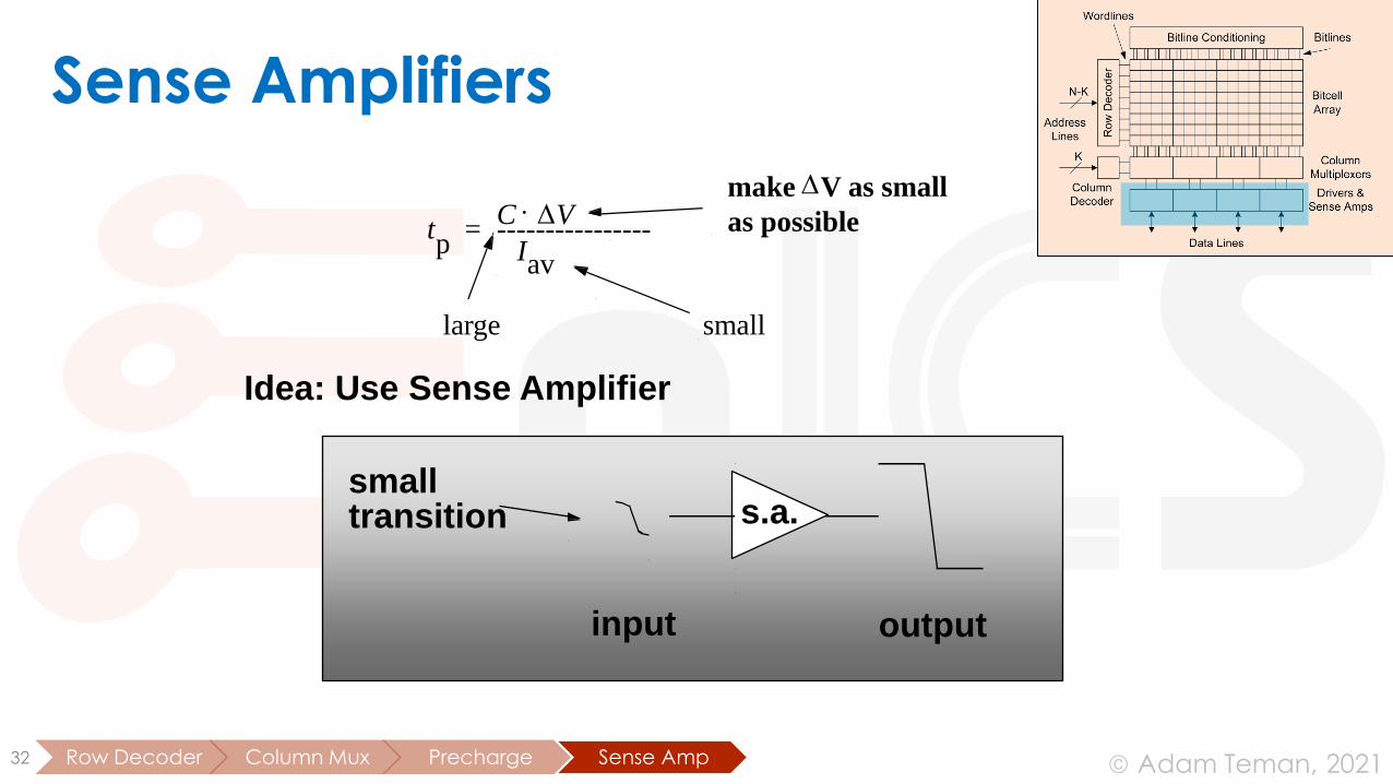
Sense Amplifiers
32
tp
C DV
Iav
----------------=
make DV as small
as possible
smalllarge
Idea: Use Sense Amplifier
outputinput
s.a.smalltransition
Row Decoder Column Mux Precharge Sense Amp

May 25, 2021© Adam Teman,
Differential Sense Amplifier
• Non-clocked Sense Amp has high static power.
• Clocked sense amp saves power
• Requires sense_clk after enough bitline swing
• Isolation transistors cut off large bitline capacitance
33 Row Decoder Column Mux Precharge Sense Amp

The Computer Hall of Fame
• The machine that many of us got to know during our military service:
• 32-bit, CISC architecture, introduced in 1977
• The VAX-11/780 was TTL-based, 5MHz, 2kB cache, reaching 1 MIPS
• Known as a “minicomputer”, even though it took up a whole room.
• VAX means “Virtual Address Extension”, since the VAX was one of the first minicomputers to use virtual memory.
• Ran the VMS operating system.
• Many systems that were developed during the cold war (e.g., F-15, F-18, Hawk missiles, nuclear programs) still use VAX today!
Source: pcworld.com

May 25, 2021© Adam Teman,
Further Reading
• Rabaey, et al. “Digital Integrated Circuits” (2nd Edition)
• Elad Alon, Berkeley ee141 (online)
• Weste, Harris, “CMOS VLSI Design (4th Edition)”
36