Embed Size (px)
Citation preview
DATA SHEET
Product specificationSupersedes data of 1999 May 17File under Integrated Circuits, IC01
2000 Jun 26
INTEGRATED CIRCUITS
SAA7324Digital servo processor andCompact Disc decoder withintegrated DAC (CD10 II)
2000 Jun 26 2
Philips Semiconductors Product specification
Digital servo processor and Compact Discdecoder with integrated DAC (CD10 II)
SAA7324
CONTENTS
1 FEATURES
2 GENERAL DESCRIPTION
3 ORDERING INFORMATION
4 QUICK REFERENCE DATA
5 BLOCK DIAGRAM
6 PINNING
7 FUNCTIONAL DESCRIPTION
7.1 Decoder part7.1.1 Principal operating modes of the decoder7.1.2 Decoding speed and crystal frequency7.1.3 Lock-to-disc mode7.1.4 Standby modes7.2 Crystal oscillator7.3 Data slicer and clock regenerator7.4 Demodulator7.4.1 Frame sync protection7.4.2 EFM demodulation7.5 Subcode data processing7.5.1 Q-channel processing7.5.2 EIAJ 3 and 4-wire subcode (CD graphics)
interfaces7.5.3 V4 subcode interface7.6 FIFO and error corrector7.6.1 Flags output (CFLG)7.7 Audio functions7.7.1 De-emphasis and phase linearity7.7.2 Digital oversampling filter7.7.3 Concealment7.7.4 Mute, full-scale, attenuation and fade7.7.5 Peak detector7.8 DAC interface7.8.1 Internal bitstream digital-to-analog
converter (DAC)7.8.2 External DAC interface7.9 EBU interface7.9.1 Format7.10 KILL circuit7.11 Audio features off7.12 The versatile pins interface7.13 Spindle motor control7.13.1 Motor output modes7.13.2 Spindle motor operating modes7.13.3 Loop characteristics7.13.4 FIFO overflow
7.14 Servo part7.14.1 Diode signal processing7.14.2 Signal conditioning7.14.3 Focus servo system7.14.4 Radial servo system7.14.5 Off-track counting7.14.6 Defect detection7.14.7 Off-track detection7.14.8 High-level features7.14.9 Driver interface7.14.10 Laser interface7.14.11 Radial shock detector7.15 Microcontroller interface7.15.1 Microcontroller interface (4-wire bus mode)7.15.2 Microcontroller interface (I2C-bus mode)7.15.3 Decoder registers and shadow registers7.15.4 Summary of functions controlled by decoder
registers 0 to F7.15.5 Summary of functions controlled by shadow
registers7.15.6 Summary of servo commands7.15.7 Summary of servo command parameters
8 LIMITING VALUES
9 CHARACTERISTICS
10 OPERATING CHARACTERISTICS(SUBCODE INTERFACE TIMING)
11 OPERATING CHARACTERISTICS (I2S-BUSTIMING)
12 OPERATING CHARACTERISTICS(MICROCONTROLLER INTERFACE TIMING)
13 APPLICATION INFORMATION
14 PACKAGE OUTLINE
15 SOLDERING
15.1 Introduction to soldering surface mountpackages
15.2 Reflow soldering15.3 Wave soldering15.4 Manual soldering15.5 Suitability of surface mount IC packages for
wave and reflow soldering methods
16 DATA SHEET STATUS
17 DEFINITIONS
18 DISCLAIMERS
19 PURCHASE OF PHILIPS I2C COMPONENTS
2000 Jun 26 3
Philips Semiconductors Product specification
Digital servo processor and Compact Discdecoder with integrated DAC (CD10 II)
SAA7324
1 FEATURES
• Integrated bitstream DAC with differential outputs,operating at 96fs with 3rd-order noise shaper; typicalperformance of −90 dB signal-to-noise ratio
• Separate serial input and output interfaces allow data‘loopback’ mode for use of onboard DAC with externalElectronic Shock Absorption (ESA) systems
• Up to 4 times speed mode
• Low voltage operation at up to 2 times speed
• Lock-to-disc mode
• Full error correction strategy, t = 2 and e = 4
• Full CD graphics interface
• All standard decoder functions implemented digitally onchip
• FIFO overflow concealment for rotational shockresistance
• Digital audio interface (EBU), audio and data
• Two and four times oversampling integrated digital filter,including fs mode
• Audio data peak level detection
• Kill interface for external DAC deactivation during digitalsilence
• All SAA737x (CD7) digital servo and high-level functions
• Low focus noise
• Same playability performance as SAA737x (CD7)
• Automatic closed-loop gain control available for focusand radial loops
• Pulsed sledge support
• Electronic damping of fast radial actuator during longjump
• Microcontroller loading LOW
• High-level servo control option
• High-level mechanism monitor
• Communication may be via TDA1301/SAA7345compatible bus or I2C-bus
• On-chip clock multiplier allows the use of 8.4672,16.9344 or 33.8688 MHz crystals or ceramicresonators.
2 GENERAL DESCRIPTION
The SAA7324 (CD10 II) is a single chip combining thefunctions of a CD decoder, digital servo and bitstreamDAC. The decoder/servo part is based on the SAA737x(CD7) and is software compatible with this design. Extrafunctions are controlled by use of ‘shadow’ registers (seeSection 7.15.3).
Supply of this Compact Disc IC does not convey animplied license under any patent right to use this IC in anyCompact Disc application.
3 ORDERING INFORMATION
TYPENUMBER
PACKAGE
NAME DESCRIPTION VERSION
SAA7324H QFP64 plastic quad flat package; 64 leads (lead length 1.6 mm);body 14 × 14 × 2.7 mm
SOT393-1
2000 Jun 26 4
Philips Semiconductors Product specification
Digital servo processor and Compact Discdecoder with integrated DAC (CD10 II)
SAA7324
4 QUICK REFERENCE DATA
Note
1. n = overspeed factor.
SYMBOL PARAMETER CONDITIONS MIN. TYP. MAX. UNIT
VDD supply voltage n = 4 mode; note 1 3.0 3.3 3.6 V
n = 1 or 2 mode; note 1 2.4 − 3.6 V
IDD supply current VDD = 3.3 V − 20 − mA
VDD = 2.4 V − 14 − mA
fxtal crystal frequency 4 8.4672 35 MHz
Tamb ambient temperature −10 − +70 °CTstg storage temperature −55 − +125 °CS/NDAC onboard DAC signal-to-noise ratio 1 kHz; 1fs; see
Figs 38 and 39−85 −90 − dB
2000 Jun 26 5
Philips Semiconductors Product specification
Digital servo processor and Compact Discdecoder with integrated DAC (CD10 II)
SAA7324
5 BLOCK DIAGRAM
handbook, full pagewidth
DECODERMICRO-
CONTROLLERINTERFACE
VERSATILE PINSINTERFACE
SUBCODEPROCESSOR
KILL
PEAKDETECT
SERIAL DATAINTERFACE
TIMING
TEST
ADC
VrefGENERATOR
FRONT-END
DIGITALPLL
MOTORCONTROL
AUDIOPROCESSOR
EBUINTERFACE
ERRORCORRECTOR
MICROCONTROLLERINTERFACE
PRE-PROCESSING
CONTROLFUNCTION
CONTROLPART
EFMDEMODULATOR
SRAM
RAMADDRESSER
OUTPUTSTAGES
FLAGS
12
13
7
40
39
41
42
2
1
3
6
25
31
44
24
16
15
26
49
48
47
46
45
43
38
63 34 61 62 32
8 9 10 11 4 14 5 17 33 50 58 52 57
54
55
56
64
59
60
53
51
30
29
28
27
VRIN
Iref
R2
SCL
SDA
RAB
SILD
HFIN
HFREF
ISLICE
TEST1
TEST2
TEST3
SELPLL
CRIN
CROUT
CL16
CL11/4
SBSY
SFSY
SUB
RCK
STATUS
R1
D1 D2 D3 D4 VSSA1
VDDA2 VSSD2
VDDD2(C)
VSSA2
VDDA1 VSSD1 VSSD3
VDDD1(P)
V1 V2/V3 V4 V5 KILL
EF
DATA
WCLK
SCLK
SERIAL DATA(LOOPBACK)INTERFACE
37
35
36SDI
WCLI
SCLI
BITSTREAMDAC
20
21
18
19LP
22RN
23RP
LN
Vpos
Vneg
DOBM
MOTO2
MOTO1
LDON
SL
FO
RA
CFLG
RESET
SAA7324
MGS174
Fig.1 Block diagram.
2000 Jun 26 6
Philips Semiconductors Product specification
Digital servo processor and Compact Discdecoder with integrated DAC (CD10 II)
SAA7324
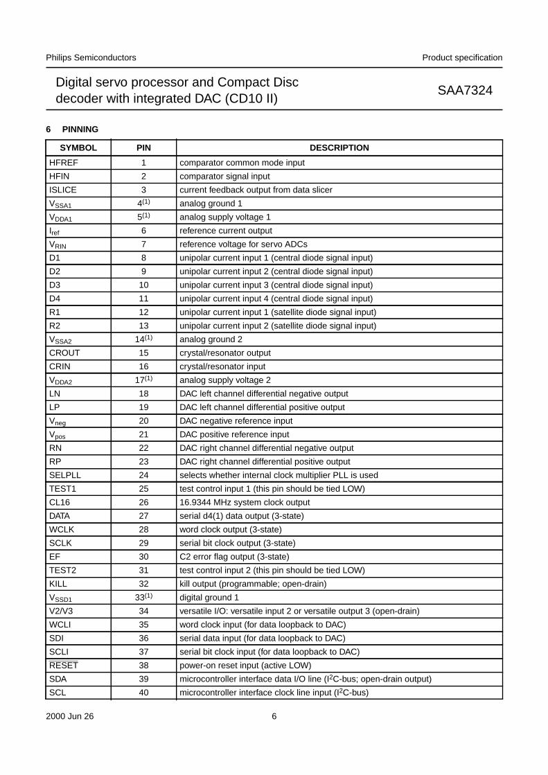
6 PINNING
SYMBOL PIN DESCRIPTION
HFREF 1 comparator common mode input
HFIN 2 comparator signal input
ISLICE 3 current feedback output from data slicer
VSSA1 4(1) analog ground 1
VDDA1 5(1) analog supply voltage 1
Iref 6 reference current output
VRIN 7 reference voltage for servo ADCs
D1 8 unipolar current input 1 (central diode signal input)
D2 9 unipolar current input 2 (central diode signal input)
D3 10 unipolar current input 3 (central diode signal input)
D4 11 unipolar current input 4 (central diode signal input)
R1 12 unipolar current input 1 (satellite diode signal input)
R2 13 unipolar current input 2 (satellite diode signal input)
VSSA2 14(1) analog ground 2
CROUT 15 crystal/resonator output
CRIN 16 crystal/resonator input
VDDA2 17(1) analog supply voltage 2
LN 18 DAC left channel differential negative output
LP 19 DAC left channel differential positive output
Vneg 20 DAC negative reference input
Vpos 21 DAC positive reference input
RN 22 DAC right channel differential negative output
RP 23 DAC right channel differential positive output
SELPLL 24 selects whether internal clock multiplier PLL is used
TEST1 25 test control input 1 (this pin should be tied LOW)
CL16 26 16.9344 MHz system clock output
DATA 27 serial d4(1) data output (3-state)
WCLK 28 word clock output (3-state)
SCLK 29 serial bit clock output (3-state)
EF 30 C2 error flag output (3-state)
TEST2 31 test control input 2 (this pin should be tied LOW)
KILL 32 kill output (programmable; open-drain)
VSSD1 33(1) digital ground 1
V2/V3 34 versatile I/O: versatile input 2 or versatile output 3 (open-drain)
WCLI 35 word clock input (for data loopback to DAC)
SDI 36 serial data input (for data loopback to DAC)
SCLI 37 serial bit clock input (for data loopback to DAC)
RESET 38 power-on reset input (active LOW)
SDA 39 microcontroller interface data I/O line (I2C-bus; open-drain output)
SCL 40 microcontroller interface clock line input (I2C-bus)
2000 Jun 26 7
Philips Semiconductors Product specification
Digital servo processor and Compact Discdecoder with integrated DAC (CD10 II)
SAA7324
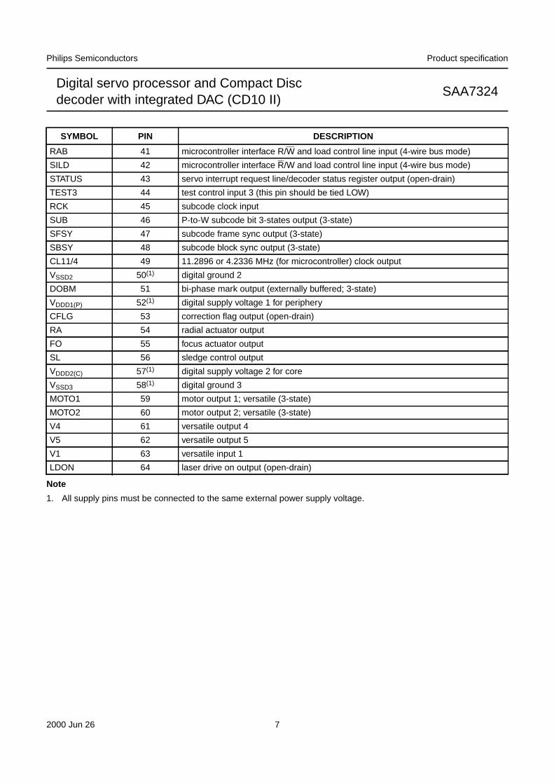
Note
1. All supply pins must be connected to the same external power supply voltage.
RAB 41 microcontroller interface R/W and load control line input (4-wire bus mode)
SILD 42 microcontroller interface R/W and load control line input (4-wire bus mode)
STATUS 43 servo interrupt request line/decoder status register output (open-drain)
TEST3 44 test control input 3 (this pin should be tied LOW)
RCK 45 subcode clock input
SUB 46 P-to-W subcode bit 3-states output (3-state)
SFSY 47 subcode frame sync output (3-state)
SBSY 48 subcode block sync output (3-state)
CL11/4 49 11.2896 or 4.2336 MHz (for microcontroller) clock output
VSSD2 50(1) digital ground 2
DOBM 51 bi-phase mark output (externally buffered; 3-state)
VDDD1(P) 52(1) digital supply voltage 1 for periphery
CFLG 53 correction flag output (open-drain)
RA 54 radial actuator output
FO 55 focus actuator output
SL 56 sledge control output
VDDD2(C) 57(1) digital supply voltage 2 for core
VSSD3 58(1) digital ground 3
MOTO1 59 motor output 1; versatile (3-state)
MOTO2 60 motor output 2; versatile (3-state)
V4 61 versatile output 4
V5 62 versatile output 5
V1 63 versatile input 1
LDON 64 laser drive on output (open-drain)
SYMBOL PIN DESCRIPTION
2000 Jun 26 8
Philips Semiconductors Product specification
Digital servo processor and Compact Discdecoder with integrated DAC (CD10 II)
SAA7324
handbook, full pagewidth
SAA7324H
MGS175
1
2
3
4
5
6
7
8
9
10
11
12
13
14
15
16
48
47
46
45
44
43
42
41
40
39
38
37
36
35
34
SBSY
SFSY
SUB
RCK
TEST3
STATUS
SILD
RAB
SCL
SDA
SCLI
SDI
WCLI
V2/V3
VSSD1
HFREF
HFIN
ISLICE
VSSA1
VDDA1
Iref
VRIN
D1
D2
D3
D4
R1
R2
VSSA2
CROUT
CRIN 33
17 18 19 20 21 22 23 24 25 26 27 28 29 30 31 32
64 63 62 61 60 59 58 57 56 55 54 53 52 51 50
LDO
N
V1
V5
V4
MO
TO
2
MO
TO
1
VS
SD
3
VD
DD
2(C
)
SL
FO
RA
CF
LG
VD
DD
1(P
)
DO
BM
VS
SD
2
CL1
1/4
VD
DA
2
LN LP
Vne
g
Vpo
s
RN
RP
SE
LPLL
TE
ST
1
CL1
6
DA
TA
WC
LK
SC
LK EF
TE
ST
2
KIL
L49
RESET
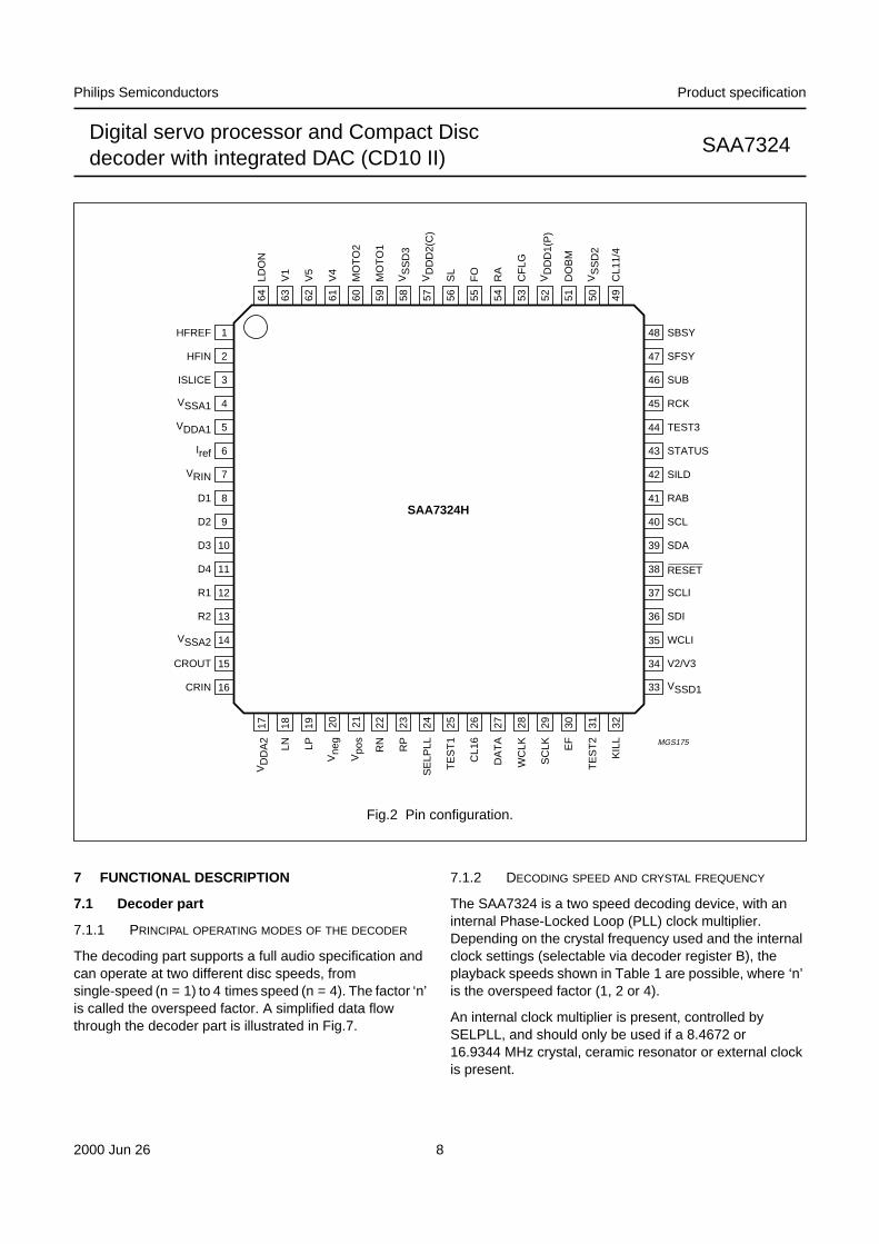
Fig.2 Pin configuration.
7 FUNCTIONAL DESCRIPTION
7.1 Decoder part
7.1.1 PRINCIPAL OPERATING MODES OF THE DECODER
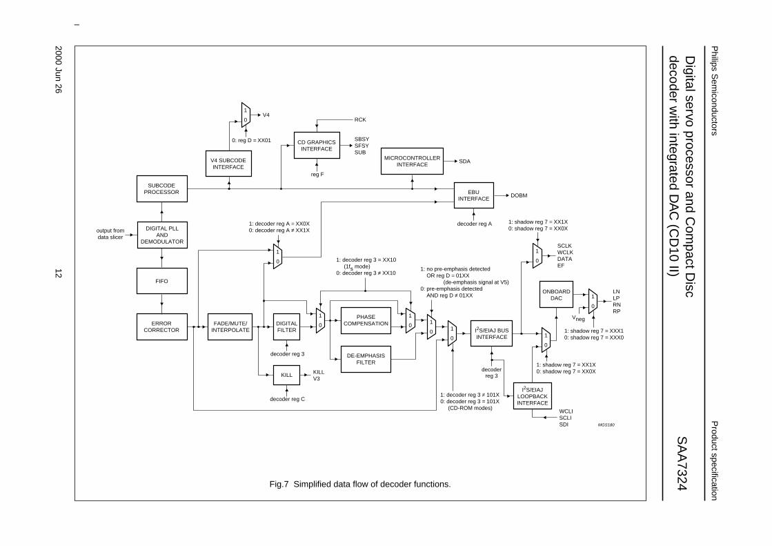
The decoding part supports a full audio specification andcan operate at two different disc speeds, fromsingle-speed (n = 1) to 4 times speed (n = 4). The factor ‘n’is called the overspeed factor. A simplified data flowthrough the decoder part is illustrated in Fig.7.
7.1.2 DECODING SPEED AND CRYSTAL FREQUENCY
The SAA7324 is a two speed decoding device, with aninternal Phase-Locked Loop (PLL) clock multiplier.Depending on the crystal frequency used and the internalclock settings (selectable via decoder register B), theplayback speeds shown in Table 1 are possible, where ‘n’is the overspeed factor (1, 2 or 4).
An internal clock multiplier is present, controlled bySELPLL, and should only be used if a 8.4672 or16.9344 MHz crystal, ceramic resonator or external clockis present.
2000 Jun 26 9
Philips Semiconductors Product specification
Digital servo processor and Compact Discdecoder with integrated DAC (CD10 II)
SAA7324
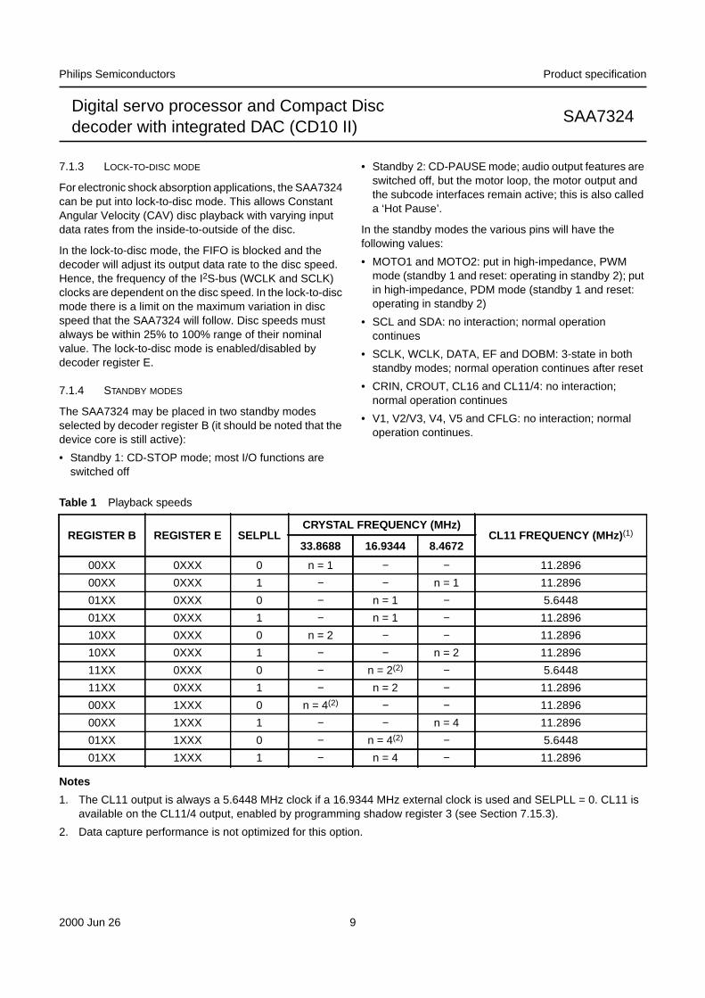
7.1.3 LOCK-TO-DISC MODE
For electronic shock absorption applications, the SAA7324can be put into lock-to-disc mode. This allows ConstantAngular Velocity (CAV) disc playback with varying inputdata rates from the inside-to-outside of the disc.
In the lock-to-disc mode, the FIFO is blocked and thedecoder will adjust its output data rate to the disc speed.Hence, the frequency of the I2S-bus (WCLK and SCLK)clocks are dependent on the disc speed. In the lock-to-discmode there is a limit on the maximum variation in discspeed that the SAA7324 will follow. Disc speeds mustalways be within 25% to 100% range of their nominalvalue. The lock-to-disc mode is enabled/disabled bydecoder register E.
7.1.4 STANDBY MODES
The SAA7324 may be placed in two standby modesselected by decoder register B (it should be noted that thedevice core is still active):
• Standby 1: CD-STOP mode; most I/O functions areswitched off
• Standby 2: CD-PAUSE mode; audio output features areswitched off, but the motor loop, the motor output andthe subcode interfaces remain active; this is also calleda ‘Hot Pause’.
In the standby modes the various pins will have thefollowing values:
• MOTO1 and MOTO2: put in high-impedance, PWMmode (standby 1 and reset: operating in standby 2); putin high-impedance, PDM mode (standby 1 and reset:operating in standby 2)
• SCL and SDA: no interaction; normal operationcontinues
• SCLK, WCLK, DATA, EF and DOBM: 3-state in bothstandby modes; normal operation continues after reset
• CRIN, CROUT, CL16 and CL11/4: no interaction;normal operation continues
• V1, V2/V3, V4, V5 and CFLG: no interaction; normaloperation continues.
Table 1 Playback speeds
Notes
1. The CL11 output is always a 5.6448 MHz clock if a 16.9344 MHz external clock is used and SELPLL = 0. CL11 isavailable on the CL11/4 output, enabled by programming shadow register 3 (see Section 7.15.3).
2. Data capture performance is not optimized for this option.
REGISTER B REGISTER E SELPLLCRYSTAL FREQUENCY (MHz)
CL11 FREQUENCY (MHz)(1)
33.8688 16.9344 8.4672
00XX 0XXX 0 n = 1 − − 11.2896
00XX 0XXX 1 − − n = 1 11.2896
01XX 0XXX 0 − n = 1 − 5.6448
01XX 0XXX 1 − n = 1 − 11.2896
10XX 0XXX 0 n = 2 − − 11.2896
10XX 0XXX 1 − − n = 2 11.2896
11XX 0XXX 0 − n = 2(2) − 5.6448
11XX 0XXX 1 − n = 2 − 11.2896
00XX 1XXX 0 n = 4(2) − − 11.2896
00XX 1XXX 1 − − n = 4 11.2896
01XX 1XXX 0 − n = 4(2) − 5.6448
01XX 1XXX 1 − n = 4 − 11.2896
2000 Jun 26 10
Philips Semiconductors Product specification
Digital servo processor and Compact Discdecoder with integrated DAC (CD10 II)
SAA7324
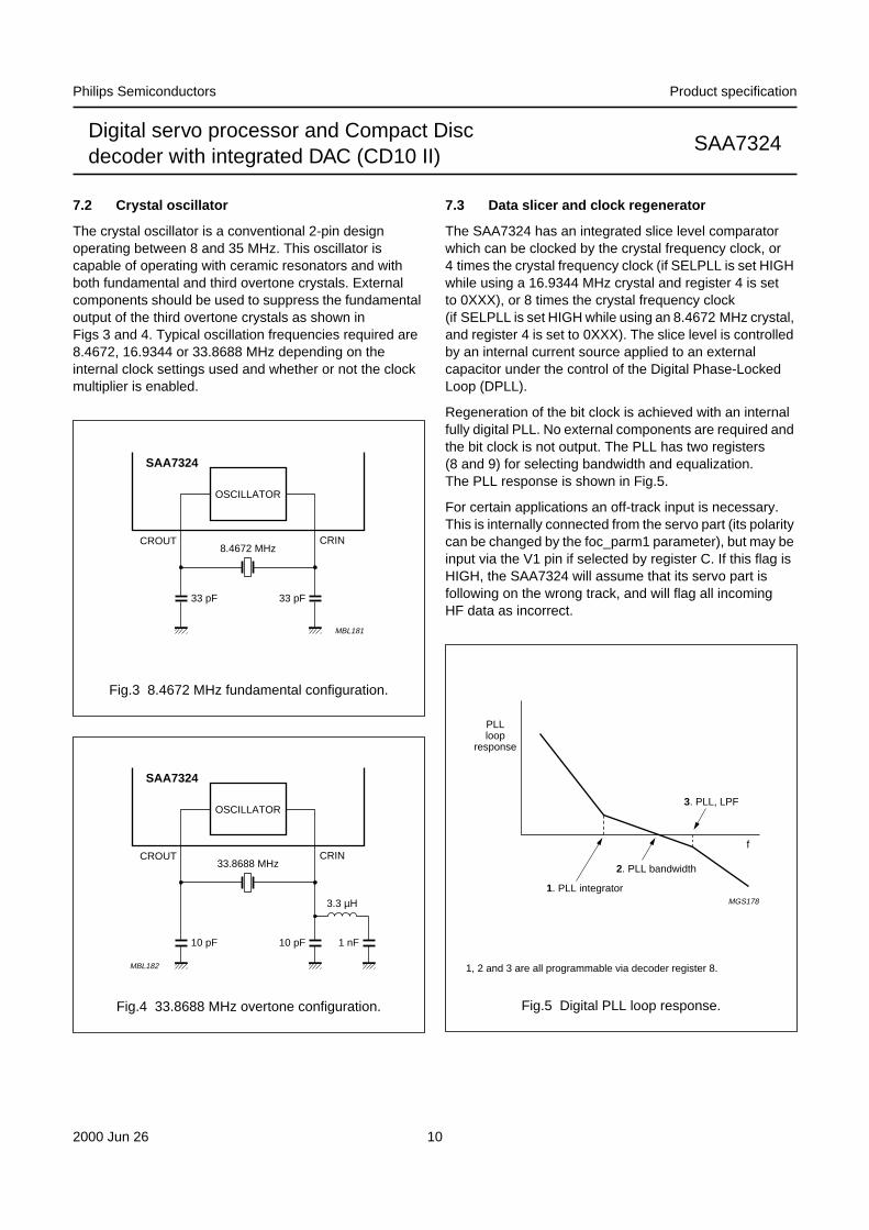
7.2 Crystal oscillator
The crystal oscillator is a conventional 2-pin designoperating between 8 and 35 MHz. This oscillator iscapable of operating with ceramic resonators and withboth fundamental and third overtone crystals. Externalcomponents should be used to suppress the fundamentaloutput of the third overtone crystals as shown inFigs 3 and 4. Typical oscillation frequencies required are8.4672, 16.9344 or 33.8688 MHz depending on theinternal clock settings used and whether or not the clockmultiplier is enabled.
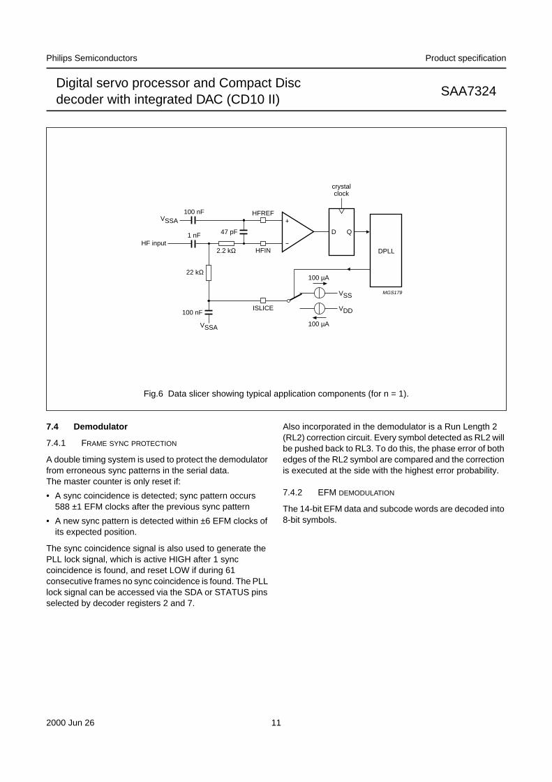
7.3 Data slicer and clock regenerator
The SAA7324 has an integrated slice level comparatorwhich can be clocked by the crystal frequency clock, or4 times the crystal frequency clock (if SELPLL is set HIGHwhile using a 16.9344 MHz crystal and register 4 is setto 0XXX), or 8 times the crystal frequency clock(if SELPLL is set HIGH while using an 8.4672 MHz crystal,and register 4 is set to 0XXX). The slice level is controlledby an internal current source applied to an externalcapacitor under the control of the Digital Phase-LockedLoop (DPLL).
Regeneration of the bit clock is achieved with an internalfully digital PLL. No external components are required andthe bit clock is not output. The PLL has two registers(8 and 9) for selecting bandwidth and equalization.The PLL response is shown in Fig.5.
For certain applications an off-track input is necessary.This is internally connected from the servo part (its polaritycan be changed by the foc_parm1 parameter), but may beinput via the V1 pin if selected by register C. If this flag isHIGH, the SAA7324 will assume that its servo part isfollowing on the wrong track, and will flag all incomingHF data as incorrect.
handbook, halfpage
OSCILLATOR
8.4672 MHzCRINCROUT
SAA7324
33 pF33 pF
MBL181
Fig.3 8.4672 MHz fundamental configuration.
handbook, halfpage
OSCILLATOR
33.8688 MHzCRINCROUT
SAA7324
3.3 µH
1 nF10 pF10 pF
MBL182
Fig.4 33.8688 MHz overtone configuration.
MGS178
handbook, halfpage
f
3. PLL, LPF
2. PLL bandwidth
1. PLL integrator
PLLloop
response
Fig.5 Digital PLL loop response.
1, 2 and 3 are all programmable via decoder register 8.
2000 Jun 26 11
Philips Semiconductors Product specification
Digital servo processor and Compact Discdecoder with integrated DAC (CD10 II)
SAA7324
47 pF
HFREF
HFIN
ISLICE
22 kΩ
2.2 kΩ
100 nF
100 nF
1 nFHF input
crystalclock
D Q
DPLL
VSSA
VSSA
VSS MGS179
VDD
100 µA
100 µA
Fig.6 Data slicer showing typical application components (for n = 1).
7.4 Demodulator
7.4.1 FRAME SYNC PROTECTION
A double timing system is used to protect the demodulatorfrom erroneous sync patterns in the serial data.The master counter is only reset if:
• A sync coincidence is detected; sync pattern occurs588 ±1 EFM clocks after the previous sync pattern
• A new sync pattern is detected within ±6 EFM clocks ofits expected position.
The sync coincidence signal is also used to generate thePLL lock signal, which is active HIGH after 1 synccoincidence is found, and reset LOW if during 61consecutive frames no sync coincidence is found. The PLLlock signal can be accessed via the SDA or STATUS pinsselected by decoder registers 2 and 7.
Also incorporated in the demodulator is a Run Length 2(RL2) correction circuit. Every symbol detected as RL2 willbe pushed back to RL3. To do this, the phase error of bothedges of the RL2 symbol are compared and the correctionis executed at the side with the highest error probability.
7.4.2 EFM DEMODULATION
The 14-bit EFM data and subcode words are decoded into8-bit symbols.
2000Jun
2612
Philips S
emiconductors
Product specification
Digital servo processor and C
ompact D
iscdecoder w
ith integrated DA
C (C
D10 II)
SA
A7324
This text is here in white to force landscape pages to be rotated correctly when browsing through the pdf in the Acrobat reader.This text is here in_white to force landscape pages to be rotated correctly when browsing through the pdf in the Acrobat reader.This text is here inThis text is here inwhite to force landscape pages to be rotated correctly when browsing through the pdf in the Acrobat reader. white to force landscape pages to be ...
dbook, full pagewidth
SUBCODEPROCESSOR
DIGITAL PLLAND
DEMODULATOR
FIFO
ERRORCORRECTOR
FADE/MUTE/INTERPOLATE
DIGITALFILTER
PHASECOMPENSATION
DE-EMPHASISFILTER
KILL
1
01
0
1
0
1
0
1
0I2S/EIAJ BUSINTERFACE
I2S/EIAJLOOPBACKINTERFACE
WCLISCLISDI
LNLPRNRP
SCLKWCLKDATAEF
decoderreg 3
Vneg
decoder reg C
decoder reg 3
reg F
decoder reg A
1
0
1: decoder reg 3 ≠ 101X0: decoder reg 3 = 101X (CD-ROM modes)
1: shadow reg 7 = XX1X0: shadow reg 7 = XX0X
1: shadow reg 7 = XX1X0: shadow reg 7 = XX0X
0: reg D = XX01
1: decoder reg A = XX0X0: decoder reg A ≠ XX1X
V4 SUBCODEINTERFACE
MICROCONTROLLERINTERFACE
CD GRAPHICSINTERFACE
EBUINTERFACE
SBSYSFSYSUB
RCK
DOBM
V4
SDA
output fromdata slicer
1: decoder reg 3 = XX10 (1fs mode)0: decoder reg 3 ≠ XX10
1: no pre-emphasis detected OR reg D = 01XX (de-emphasis signal at V5)0: pre-emphasis detected AND reg D ≠ 01XX
KILLV3
MGS180
1
0
ONBOARDDAC
1: shadow reg 7 = XXX10: shadow reg 7 = XXX0
1
0
1
0
Fig.7 Simplified data flow of decoder functions.
2000 Jun 26 13
Philips Semiconductors Product specification
Digital servo processor and Compact Discdecoder with integrated DAC (CD10 II)
SAA7324
7.5 Subcode data processing
7.5.1 Q-CHANNEL PROCESSING
The 96-bit Q-channel word is accumulated in an internalbuffer. The last 16 bits are used internally to perform aCyclic Redundancy Check (CRC). If the data is good, theSUBQREADY-I signal will go LOW. SUBQREADY-I canbe read via the SDA or STATUS pins, selected via decoderregister 2. Good Q-channel data may be read from SDA.
7.5.2 EIAJ 3 AND 4-WIRE SUBCODE (CD GRAPHICS)INTERFACES
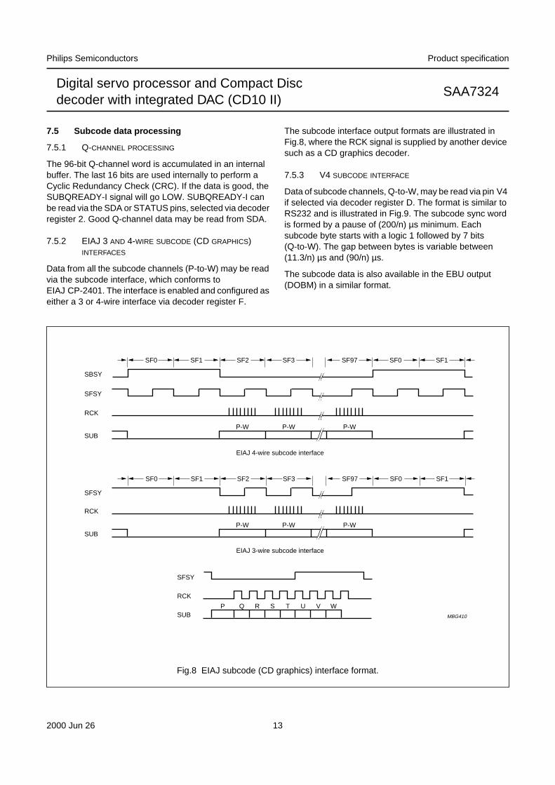
Data from all the subcode channels (P-to-W) may be readvia the subcode interface, which conforms toEIAJ CP-2401. The interface is enabled and configured aseither a 3 or 4-wire interface via decoder register F.
The subcode interface output formats are illustrated inFig.8, where the RCK signal is supplied by another devicesuch as a CD graphics decoder.
7.5.3 V4 SUBCODE INTERFACE
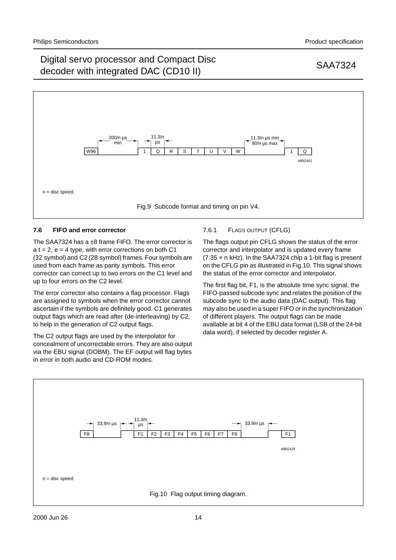
Data of subcode channels, Q-to-W, may be read via pin V4if selected via decoder register D. The format is similar toRS232 and is illustrated in Fig.9. The subcode sync wordis formed by a pause of (200/n) µs minimum. Eachsubcode byte starts with a logic 1 followed by 7 bits(Q-to-W). The gap between bytes is variable between(11.3/n) µs and (90/n) µs.
The subcode data is also available in the EBU output(DOBM) in a similar format.
handbook, full pagewidth
SBSY
SFSY
RCK
SUB
SFSY
RCK
SUB
SFSY
RCK
SUB
EIAJ 4-wire subcode interface
EIAJ 3-wire subcode interface
SF0 SF1 SF2 SF3 SF97 SF0 SF1
P-W P-W P-W
P-W P-W P-W
P Q R S T U V W
MBG410
SF0 SF1 SF2 SF3 SF97 SF0 SF1
Fig.8 EIAJ subcode (CD graphics) interface format.
2000 Jun 26 14
Philips Semiconductors Product specification
Digital servo processor and Compact Discdecoder with integrated DAC (CD10 II)
SAA7324
W96 1 Q R S T U V W 1 Q
200/n µsmin
11.3/nµs
11.3/n µs min90/n µs max
MBG401
Fig.9 Subcode format and timing on pin V4.
n = disc speed.
7.6 FIFO and error corrector
The SAA7324 has a ±8 frame FIFO. The error corrector isa t = 2, e = 4 type, with error corrections on both C1(32 symbol) and C2 (28 symbol) frames. Four symbols areused from each frame as parity symbols. This errorcorrector can correct up to two errors on the C1 level andup to four errors on the C2 level.
The error corrector also contains a flag processor. Flagsare assigned to symbols when the error corrector cannotascertain if the symbols are definitely good. C1 generatesoutput flags which are read after (de-interleaving) by C2,to help in the generation of C2 output flags.
The C2 output flags are used by the interpolator forconcealment of uncorrectable errors. They are also outputvia the EBU signal (DOBM). The EF output will flag bytesin error in both audio and CD-ROM modes.
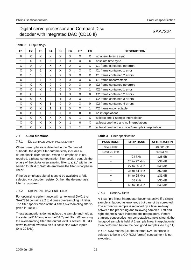
7.6.1 FLAGS OUTPUT (CFLG)
The flags output pin CFLG shows the status of the errorcorrector and interpolator and is updated every frame(7.35 × n kHz). In the SAA7324 chip a 1-bit flag is presenton the CFLG pin as illustrated in Fig.10. This signal showsthe status of the error corrector and interpolator.
The first flag bit, F1, is the absolute time sync signal, theFIFO-passed subcode sync and relates the position of thesubcode sync to the audio data (DAC output). This flagmay also be used in a super FIFO or in the synchronizationof different players. The output flags can be madeavailable at bit 4 of the EBU data format (LSB of the 24-bitdata word), if selected by decoder register A.
handbook, full pagewidth
F1 F2 F3 F4 F5 F6 F7 F8 F1F8
11.3/nµs 33.9/n µs33.9/n µs
MBG425
Fig.10 Flag output timing diagram.
n = disc speed.
2000 Jun 26 15
Philips Semiconductors Product specification
Digital servo processor and Compact Discdecoder with integrated DAC (CD10 II)
SAA7324
Table 2 Output flags
F1 F2 F3 F4 F5 F6 F7 F8 DESCRIPTION
0 X X X X X X X no absolute time sync
1 X X X X X X X absolute time sync
X 0 0 X X X X X C1 frame contained no errors
X 0 1 X X X X X C1 frame contained 1 error
X 1 0 X X X X X C1 frame contained 2 errors
X 1 1 X X X X X C1 frame uncorrectable
X X X 0 0 X X 0 C2 frame contained no errors
X X X 0 0 X X 1 C2 frame contained 1 error
X X X 0 1 X X 0 C2 frame contained 2 errors
X X X 0 1 X X 1 C2 frame contained 3 errors
X X X 1 0 X X 0 C2 frame contained 4 errors
X X X 1 1 X X 1 C2 frame uncorrectable
X X X X X 0 0 X no interpolations
X X X X X 0 1 X at least one 1-sample interpolation
X X X X X 1 0 X at least one hold and no interpolations
X X X X X 1 1 X at least one hold and one 1-sample interpolation
7.7 Audio functions
7.7.1 DE-EMPHASIS AND PHASE LINEARITY
When pre-emphasis is detected in the Q-channelsubcode, the digital filter automatically includes ade-emphasis filter section. When de-emphasis is notrequired, a phase compensation filter section controls thephase of the digital oversampling filter to ≤ ±1° within theband 0 to 16 kHz. With de-emphasis the filter is not phaselinear.
If the de-emphasis signal is set to be available at V5,selected via decoder register D, then the de-emphasisfilter is bypassed.
7.7.2 DIGITAL OVERSAMPLING FILTER
For optimizing performance with an external DAC, theSAA7324 contains a 2 to 4 times oversampling IIR filter.The filter specification of the 4 times oversampling filter isgiven in Table 3.
These attenuations do not include the sample-and-hold atthe external DAC output or the DAC post filter. When usingthe oversampling filter, the output level is scaled −0.5 dBdown to avoid overflow on full-scale sine wave inputs(0 to 20 kHz).
Table 3 Filter specification
7.7.3 CONCEALMENT
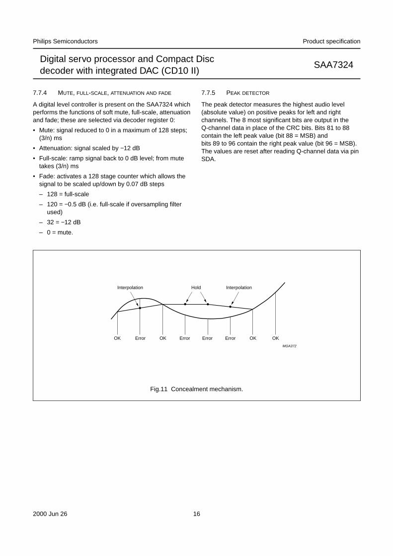
A 1-sample linear interpolator becomes active if a singlesample is flagged as erroneous but cannot be corrected.The erroneous sample is replaced by a level midwaybetween the preceding and following samples. Left andright channels have independent interpolators. If morethan one consecutive non-correctable sample is found, thelast good sample is held. A 1-sample linear interpolation isthen performed before the next good sample (see Fig.11).
In CD-ROM modes (i.e. the external DAC interface isselected to be in a CD-ROM format) concealment is notexecuted.
PASS BAND STOP BAND ATTENUATION
0 to 9 kHz − ≤0.001 dB
19 to 20 kHz − ≤0.03 dB
− 24 kHz ≥25 dB
− 24 to 27 kHz ≥38 dB
− 27 to 35 kHz ≥40 dB
− 35 to 64 kHz ≥50 dB
− 64 to 68 kHz ≥31 dB
− 68 kHz ≥35 dB
− 69 to 88 kHz ≥40 dB
2000 Jun 26 16
Philips Semiconductors Product specification
Digital servo processor and Compact Discdecoder with integrated DAC (CD10 II)
SAA7324
7.7.4 MUTE, FULL-SCALE, ATTENUATION AND FADE
A digital level controller is present on the SAA7324 whichperforms the functions of soft mute, full-scale, attenuationand fade; these are selected via decoder register 0:
• Mute: signal reduced to 0 in a maximum of 128 steps;(3/n) ms
• Attenuation: signal scaled by −12 dB
• Full-scale: ramp signal back to 0 dB level; from mutetakes (3/n) ms
• Fade: activates a 128 stage counter which allows thesignal to be scaled up/down by 0.07 dB steps
– 128 = full-scale
– 120 = −0.5 dB (i.e. full-scale if oversampling filterused)
– 32 = −12 dB
– 0 = mute.
7.7.5 PEAK DETECTOR
The peak detector measures the highest audio level(absolute value) on positive peaks for left and rightchannels. The 8 most significant bits are output in theQ-channel data in place of the CRC bits. Bits 81 to 88contain the left peak value (bit 88 = MSB) andbits 89 to 96 contain the right peak value (bit 96 = MSB).The values are reset after reading Q-channel data via pinSDA.
Interpolation Hold Interpolation
MGA372
OK Error OK Error Error Error OK OK
Fig.11 Concealment mechanism.
2000 Jun 26 17
Philips Semiconductors Product specification
Digital servo processor and Compact Discdecoder with integrated DAC (CD10 II)
SAA7324
7.8 DAC interface
7.8.1 INTERNAL BITSTREAM DIGITAL-TO-ANALOG CONVERTER (DAC)
The onboard bitstream DAC operates at a clock frequency of 96fs and is designed for operation with an audio input at 1fs.Optimum performance is dependent on the application circuit used and careful consideration should be given to therecommended application circuits shown in Figs 38 and 39. The onboard DAC is controlled from shadow register 7(see Section 7.15.3 for definition of shadow registers). This shadow register controls routing of data into the onboardDAC and also controls the DAC output pins, which can be held at zero when the onboard DAC is not required; seeTable 4:
Audio data from the decoder part of the SAA7324 can be routed as described in Sections 7.8.1.1 and 7.8.1.2.
Table 4 Shadow register
SHADENSHADOWADDRESS
REGISTER DATA FUNCTION RESET
1 0111 (7H) control ofonboard DAC
XXX0 hold onboard DAC outputs at zero reset
XXX1 enable onboard DAC outputs −XX0X use external DAC or route audio data into
onboard DAC (loopback mode)reset
XX1X route audio data into onboard DAC(non-loopback mode)
−
7.8.1.1 Use onboard DAC
Setting shadow register 7 to XX11 will route audio datafrom the CD10 decoder into the internal DAC, and enablesthe DAC output pins (LN, LP, RN and RP). To enable theon-board DAC, the DAC interface format (set by register 3)must be set to 16-bit 1fs mode, either I2S or EIAJ format.CD-ROM mode can also be used if interpolation is notrequired. The serial data output pins for interfacing with anexternal DAC (SCLK, WCLK, DATA and EF) are set tohigh-impedance.
7.8.1.2 Loopback external data into onboard DAC
The onboard DAC can also be set to accept serial datainputs from an external source, e.g. an Electronic ShockAbsorption (ESA) IC. This is known as loopback mode andis enabled by setting shadow register 7 to XX01.
This enables the serial data output pins (SCLK, WCLK,DATA and EF) so that data can be routed from theSAA7324 to an external ESA system (or external DAC).
The serial data from an external ESA IC can then also beinput to the onboard DAC on the SAA7324 by utilising theserial data input interface (SCLI, SDI and WCLI).
In this mode, a wide range of data formats to the externalESA IC can be programmed as shown in Table 5.However, the serial input on the SAA7324 will alwaysexpect the input data from the ESA IC to be 16-bit 1fs andthe same data format, either I2S-bus or EIAJ, as the serialoutput format (set by decoder register 3).
2000 Jun 26 18
Philips Semiconductors Product specification
Digital servo processor and Compact Discdecoder with integrated DAC (CD10 II)
SAA7324
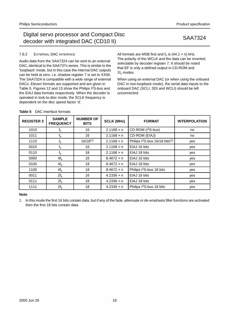
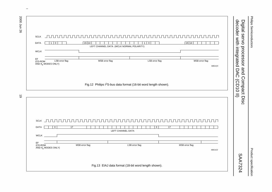
7.8.2 EXTERNAL DAC INTERFACE
Audio data from the SAA7324 can be sent to an externalDAC, identical to the SAA737x series. This is similar to the‘loopback’ mode, but in this case the internal DAC outputscan be held at zero. i.e. shadow register 7 is set to XX00.The SAA7324 is compatible with a wide range of externalDACs. Eleven formats are supported and are given inTable 5. Figures 12 and 13 show the Philips I2S-bus andthe EIAJ data formats respectively. When the decoder isoperated in lock-to-disc mode, the SCLK frequency isdependent on the disc speed factor ‘d’.
All formats are MSB first and fs is (44.1 × n) kHz.The polarity of the WCLK and the data can be inverted;selectable by decoder register 7. It should be notedthat EF is only a defined output in CD-ROM and1fs modes.
When using an external DAC (or when using the onboardDAC in non-loopback mode), the serial data inputs to theonboard DAC (SCLI, SDI and WCLI) should be leftunconnected.
Table 5 DAC interface formats
Note
1. In this mode the first 16 bits contain data, but if any of the fade, attenuate or de-emphasis filter functions are activatedthen the first 18 bits contain data.
REGISTER 3SAMPLE
FREQUENCYNUMBER OF
BITSSCLK (MHz) FORMAT INTERPOLATION
1010 fs 16 2.1168 × n CD-ROM (I2S-bus) no
1011 fs 16 2.1168 × n CD-ROM (EIAJ) no
1110 fs 16/18(1) 2.1168 × n Philips I2S-bus 16/18 bits(1) yes
0010 fs 16 2.1168 × n EIAJ 16 bits yes
0110 fs 18 2.1168 × n EIAJ 18 bits yes
0000 4fs 16 8.4672 × n EIAJ 16 bits yes
0100 4fs 18 8.4672 × n EIAJ 18 bits yes
1100 4fs 18 8.4672 × n Philips I2S-bus 18 bits yes
0011 2fs 16 4.2336 × n EIAJ 16 bits yes
0111 2fs 18 4.2336 × n EIAJ 18 bits yes
1111 2fs 18 4.2336 × n Philips I2S-bus 18 bits yes
2000Jun
2619
Philips S
emiconductors
Product specification
Digital servo processor and C
ompact D
iscdecoder w
ith integrated DA
C (C
D10 II)
SA
A7324
This text is here in white to force landscape pages to be rotated correctly when browsing through the pdf in the Acrobat reader.This text is here in_white to force landscape pages to be rotated correctly when browsing through the pdf in the Acrobat reader.This text is here inThis text is here inwhite to force landscape pages to be rotated correctly when browsing through the pdf in the Acrobat reader. white to force landscape pages to be ...
LEFT CHANNEL DATA (WCLK NORMAL POLARITY)
SCLK
15 14 15 141 0DATA
WCLK
LSB error flag MSB error flag LSB error flag MSB error flag EF(CD-ROMAND Ifs MODES ONLY)
01
MBG424
Fig.12 Philips I2S-bus data format (16-bit word length shown).
SCLK
17 170DATA
WCLK
0
LEFT CHANNEL DATA
MSB error flag LSB error flag MSB error flag
MBG423
EF(CD-ROMAND Ifs MODES ONLY)
Fig.13 EIAJ data format (18-bit word length shown).
2000 Jun 26 20
Philips Semiconductors Product specification
Digital servo processor and Compact Discdecoder with integrated DAC (CD10 II)
SAA7324
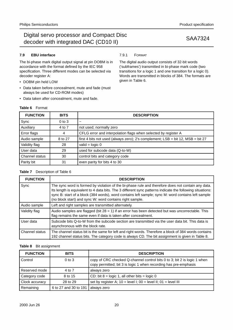
7.9 EBU interface
The bi-phase mark digital output signal at pin DOBM is inaccordance with the format defined by the IEC 958specification. Three different modes can be selected viadecoder register A:
• DOBM pin held LOW
• Data taken before concealment, mute and fade (mustalways be used for CD-ROM modes)
• Data taken after concealment, mute and fade.
7.9.1 FORMAT
The digital audio output consists of 32-bit words(‘subframes’) transmitted in bi-phase mark code (twotransitions for a logic 1 and one transition for a logic 0).Words are transmitted in blocks of 384. The formats aregiven in Table 6.
Table 6 Format
Table 7 Description of Table 6
Table 8 Bit assignment
FUNCTION BITS DESCRIPTION
Sync 0 to 3 −Auxiliary 4 to 7 not used; normally zero
Error flags 4 CFLG error and interpolation flags when selected by register A
Audio sample 8 to 27 first 4 bits not used (always zero); 2’s complement; LSB = bit 12, MSB = bit 27
Validity flag 28 valid = logic 0
User data 29 used for subcode data (Q-to-W)
Channel status 30 control bits and category code
Parity bit 31 even parity for bits 4 to 30
FUNCTION DESCRIPTION
Sync The sync word is formed by violation of the bi-phase rule and therefore does not contain any data.Its length is equivalent to 4 data bits. The 3 different sync patterns indicate the following situations:sync B: start of a block (384 words), word contains left sample; sync M: word contains left sample(no block start) and sync W: word contains right sample.
Audio sample Left and right samples are transmitted alternately.
Validity flag Audio samples are flagged (bit 28 = 1) if an error has been detected but was uncorrectable. Thisflag remains the same even if data is taken after concealment.
User data Subcode bits Q-to-W from the subcode section are transmitted via the user data bit. This data isasynchronous with the block rate.
Channel status The channel status bit is the same for left and right words. Therefore a block of 384 words contains192 channel status bits. The category code is always CD. The bit assignment is given in Table 8.
FUNCTION BITS DESCRIPTION
Control 0 to 3 copy of CRC checked Q-channel control bits 0 to 3; bit 2 is logic 1 whencopy permitted; bit 3 is logic 1 when recording has pre-emphasis
Reserved mode 4 to 7 always zero
Category code 8 to 15 CD: bit 8 = logic 1, all other bits = logic 0
Clock accuracy 28 to 29 set by register A; 10 = level I; 00 = level II; 01 = level III
Remaining 6 to 27 and 30 to 191 always zero
2000 Jun 26 21
Philips Semiconductors Product specification
Digital servo processor and Compact Discdecoder with integrated DAC (CD10 II)
SAA7324
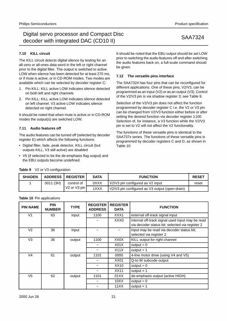
7.10 KILL circuit
The KILL circuit detects digital silence by testing for anall-zero or all-ones data word in the left or right channelprior to the digital filter. The output is switched to activeLOW when silence has been detected for at least 270 ms,or if mute is active, or in CD-ROM modes. Two modes areavailable which can be selected by decoder register C:
1. Pin KILL: KILL active LOW indicates silence detectedon both left and right channels
2. Pin KILL: KILL active LOW indicates silence detectedon left channel. V3 active LOW indicates silencedetected on right channel.
It should be noted that when mute is active or in CD-ROMmodes the output(s) are switched LOW.
7.11 Audio features off
The audio features can be turned off (selected by decoderregister E) which affects the following functions:
• Digital filter, fade, peak detector, KILL circuit (butoutputs KILL, V3 still active) are disabled
• V5 (if selected to be the de-emphasis flag output) andthe EBU outputs become undefined.
It should be noted that the EBU output should be set LOWprior to switching the audio features off and after switchingthe audio features back on, a full-scale command shouldbe given.
7.12 The versatile pins interface
The SAA7324 has four pins that can be reconfigured fordifferent applications. One of these pins, V2/V3, can beprogrammed as an input (V2) or as an output (V3). Controlof the V2/V3 pin is via shadow register 3; see Table 9.
Selection of the V2/V3 pin does not affect the functionprogrammed by decoder register C i.e. the V2 or V3 pincan be changed from V2/V3 function either before or aftersetting the desired function via decoder register 1100.Selection of, for instance, a V3 function while the V2/V3pin is set to V2 will not affect the V2 functionality.
The functions of these versatile pins is identical to theSAA737x series. The functions of these versatile pins isprogrammed by decoder registers C and D, as shown inTable 10.
Table 9 V2 or V3 configuration
Table 10 Pin applications
SHADEN ADDRESS REGISTER DATA FUNCTION RESET
1 0011 (3H) control ofV2 or V3 pin
0XXX V2/V3 pin configured as V2 input reset
1XXX V2/V3 pin configured as V3 output (open-drain)
PIN NAMEPIN
NUMBERTYPE
REGISTERADDRESS
REGISTERDATA
FUNCTION
V1 63 input 1100 XXX1 external off-track signal input− XXX0 internal off-track signal used input may be read
via decoder status bit; selected via register 2V2 36 input − − input may be read via decoder status bit;
selected via register 2V3 36 output 1100 XX0X KILL output for right channel
− X01X output = 0− X11X output = 1
V4 61 output 1101 0000 4-line motor drive (using V4 and V5)− XX01 Q-to-W subcode output− XX10 output = 0− XX11 output = 1
V5 62 output 1101 01XX de-emphasis output (active HIGH)− 10XX output = 0− 11XX output = 1
2000 Jun 26 22
Philips Semiconductors Product specification
Digital servo processor and Compact Discdecoder with integrated DAC (CD10 II)
SAA7324
7.13 Spindle motor control
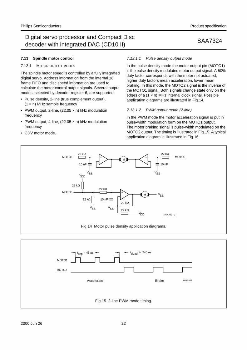
7.13.1 MOTOR OUTPUT MODES
The spindle motor speed is controlled by a fully integrateddigital servo. Address information from the internal ±8frame FIFO and disc speed information are used tocalculate the motor control output signals. Several outputmodes, selected by decoder register 6, are supported:
• Pulse density, 2-line (true complement output),(1 × n) MHz sample frequency
• PWM output, 2-line, (22.05 × n) kHz modulationfrequency
• PWM output, 4-line, (22.05 × n) kHz modulationfrequency
• CDV motor mode.
7.13.1.1 Pulse density output mode
In the pulse density mode the motor output pin (MOTO1)is the pulse density modulated motor output signal. A 50%duty factor corresponds with the motor not actuated,higher duty factors mean acceleration, lower meanbraking. In this mode, the MOTO2 signal is the inverse ofthe MOTO1 signal. Both signals change state only on theedges of a (1 × n) MHz internal clock signal. Possibleapplication diagrams are illustrated in Fig.14.
7.13.1.2 PWM output mode (2-line)
In the PWM mode the motor acceleration signal is put inpulse-width modulation form on the MOTO1 output.The motor braking signal is pulse-width modulated on theMOTO2 output. The timing is illustrated in Fig.15. A typicalapplication diagram is illustrated in Fig.16.
MGA363 - 1
MOTO2
VDD
VSS
MOTO1M
22 kΩ
10 nF
+–
22 kΩ
10 nF
+–
VSS
VSSMOTO1
M
22 kΩ
10 nF
+–
22 kΩ
22 kΩVSS
VDD
VSS
22 kΩ
22 kΩ
Fig.14 Motor pulse density application diagrams.
rept = 45 µs t 240 nsdead
Accelerate Brake
MOTO1
MOTO2
MGA366
Fig.15 2-line PWM mode timing.
2000 Jun 26 23
Philips Semiconductors Product specification
Digital servo processor and Compact Discdecoder with integrated DAC (CD10 II)
SAA7324
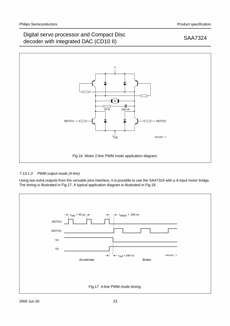
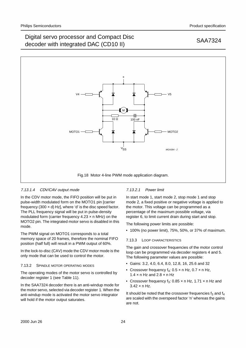
7.13.1.3 PWM output mode (4-line)
Using two extra outputs from the versatile pins interface, it is possible to use the SAA7324 with a 4-input motor bridge.The timing is illustrated in Fig.17. A typical application diagram is illustrated in Fig.18.
MGA365 - 2VSS
+
M
MOTO1 MOTO2
10 Ω 100 nF
Fig.16 Motor 2-line PWM mode application diagram.
MOTO1
MOTO2
V4
V5
rept = 45 µs t 240 nsdead
ovlt = 240 ns
Accelerate Brake
MGA367 - 1
Fig.17 4-line PWM mode timing.
2000 Jun 26 24
Philips Semiconductors Product specification
Digital servo processor and Compact Discdecoder with integrated DAC (CD10 II)
SAA7324
MGA364 - 2VSS
+
M
MOTO1
V4
MOTO2
V5
100 nF10 Ω
Fig.18 Motor 4-line PWM mode application diagram.
7.13.1.4 CDV/CAV output mode
In the CDV motor mode, the FIFO position will be put inpulse-width modulated form on the MOTO1 pin [carrierfrequency (300 × d) Hz], where ‘d’ is the disc speed factor.The PLL frequency signal will be put in pulse-densitymodulated form (carrier frequency 4.23 × n MHz) on theMOTO2 pin. The integrated motor servo is disabled in thismode.
The PWM signal on MOTO1 corresponds to a totalmemory space of 20 frames, therefore the nominal FIFOposition (half full) will result in a PWM output of 60%.
In the lock-to-disc (CAV) mode the CDV motor mode is theonly mode that can be used to control the motor.
7.13.2 SPINDLE MOTOR OPERATING MODES
The operating modes of the motor servo is controlled bydecoder register 1 (see Table 11).
In the SAA7324 decoder there is an anti-windup mode forthe motor servo, selected via decoder register 1. When theanti-windup mode is activated the motor servo integratorwill hold if the motor output saturates.
7.13.2.1 Power limit
In start mode 1, start mode 2, stop mode 1 and stopmode 2, a fixed positive or negative voltage is applied tothe motor. This voltage can be programmed as apercentage of the maximum possible voltage, viaregister 6, to limit current drain during start and stop.
The following power limits are possible:
• 100% (no power limit), 75%, 50%, or 37% of maximum.
7.13.3 LOOP CHARACTERISTICS
The gain and crossover frequencies of the motor controlloop can be programmed via decoder registers 4 and 5.The following parameter values are possible:
• Gains: 3.2, 4.0, 6.4, 8.0, 12.8, 16, 25.6 and 32
• Crossover frequency f4: 0.5 × n Hz, 0.7 × n Hz,1.4 × n Hz and 2.8 × n Hz
• Crossover frequency f3: 0.85 × n Hz, 1.71 × n Hz and3.42 × n Hz.
It should be noted that the crossover frequencies f3 and f4are scaled with the overspeed factor ‘n’ whereas the gainsare not.
2000 Jun 26 25
Philips Semiconductors Product specification
Digital servo processor and Compact Discdecoder with integrated DAC (CD10 II)
SAA7324
7.13.4 FIFO OVERFLOW
If FIFO overflow occurs during Play mode (e.g.: as a result of motor rotational shock), the FIFO will be automatically resetto 50% and the audio interpolator tries to conceal as much as possible to minimize the effect of data loss.
Table 11 Operating modes
MODE DESCRIPTION
Start mode 1 The disc is accelerated by applying a positive voltage to the spindle motor. No decisions are involvedand the PLL is reset. No disc speed information is available for the microcontroller.
Start mode 2 The disc is accelerated as in start mode 1, however the PLL will monitor the disc speed. When thedisc reaches 75% of its nominal speed, the controller will switch to jump mode. The motor statussignals selectable via register 2 are valid.
Jump mode Motor servo enabled but FIFO kept reset at 50%, integrator is held. The audio is muted but it ispossible to read the subcode. It should be noted that in the CD-ROM modes the data, on EBU andthe I2S-bus is not muted.
Jump mode 1 Similar to jump mode but motor integrator is kept at zero. Used for long jumps where there is a largechange in disc speed.
Play mode FIFO released after resetting to 50%. Audio mute released.
Stop mode 1 Disc is braked by applying a negative voltage to the motor. No decisions are involved.
Stop mode 2 The disc is braked as in stop mode 1 but the PLL will monitor the disc speed. As soon as the discreaches 12% (or 6%, depending on the programmed brake percentage, via register E) of its nominalspeed, the MOTSTOP status signal will go HIGH and switch the motor servo to Off mode.
Off mode Motor not steered.
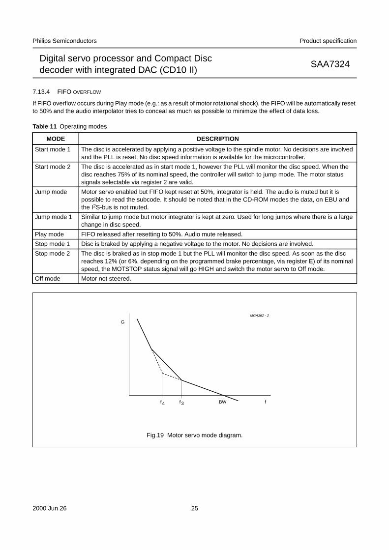
MGA362 - 2
G
f4f BW3f
Fig.19 Motor servo mode diagram.
2000 Jun 26 26
Philips Semiconductors Product specification
Digital servo processor and Compact Discdecoder with integrated DAC (CD10 II)
SAA7324
7.14 Servo part
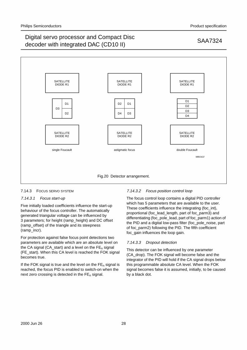
7.14.1 DIODE SIGNAL PROCESSING
The photo detector in conventional two-stage three-beamCompact Disc systems normally contains six discretediodes. Four of these diodes (three for single foucaultsystems) carry the Central Aperture signal (CA) while theother two diodes (satellite diodes) carry the radial trackinginformation. The CA signal is processed into an HF signal(for the decoder function) and LF signal (information forthe focus servo loop) before it is supplied to the SAA7324.
The analog signals from the central and satellite diodesare converted into a digital representation usingAnalog-to-Digital Converters (ADCs).
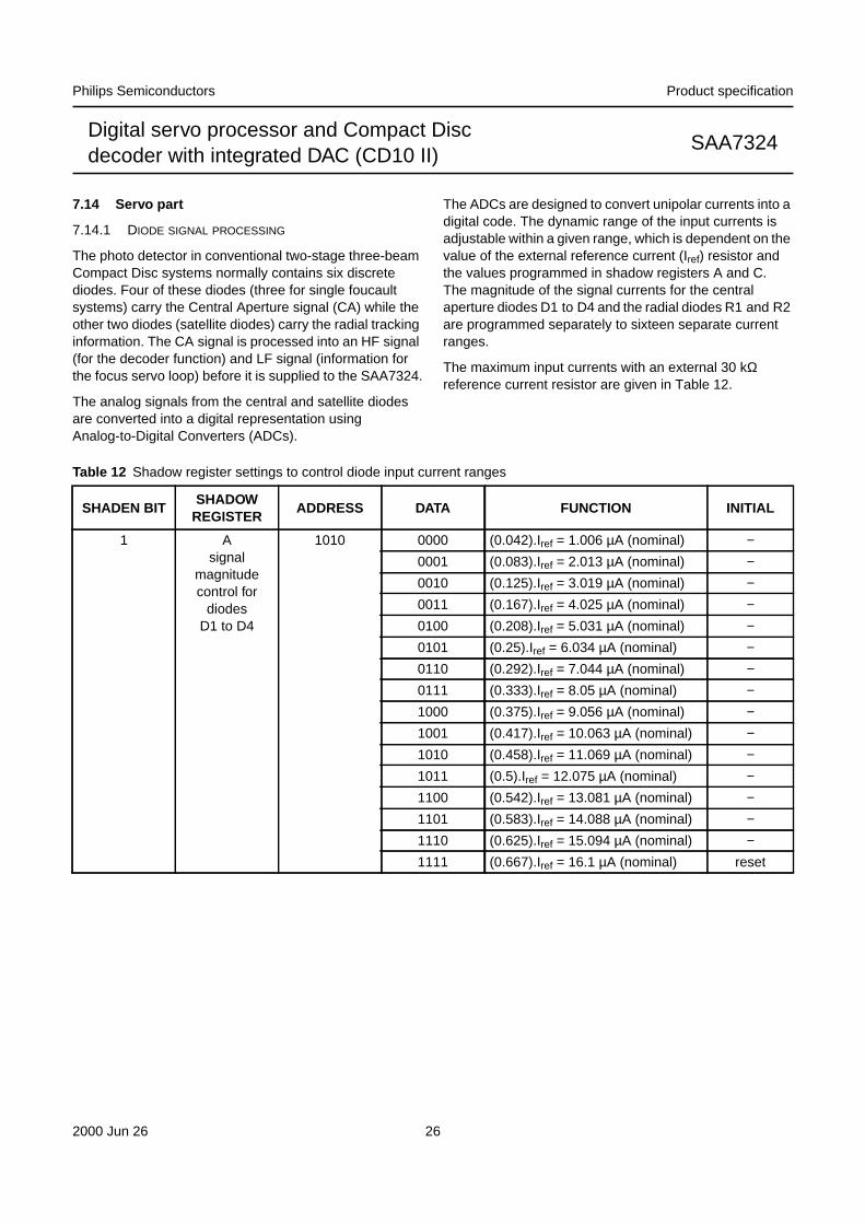
The ADCs are designed to convert unipolar currents into adigital code. The dynamic range of the input currents isadjustable within a given range, which is dependent on thevalue of the external reference current (Iref) resistor andthe values programmed in shadow registers A and C.The magnitude of the signal currents for the centralaperture diodes D1 to D4 and the radial diodes R1 and R2are programmed separately to sixteen separate currentranges.
The maximum input currents with an external 30 kΩreference current resistor are given in Table 12.
Table 12 Shadow register settings to control diode input current ranges
SHADEN BITSHADOW
REGISTERADDRESS DATA FUNCTION INITIAL
1 Asignal
magnitudecontrol for
diodesD1 to D4
1010 0000 (0.042).Iref = 1.006 µA (nominal) −0001 (0.083).Iref = 2.013 µA (nominal) −0010 (0.125).Iref = 3.019 µA (nominal) −0011 (0.167).Iref = 4.025 µA (nominal) −0100 (0.208).Iref = 5.031 µA (nominal) −0101 (0.25).Iref = 6.034 µA (nominal) −0110 (0.292).Iref = 7.044 µA (nominal) −0111 (0.333).Iref = 8.05 µA (nominal) −1000 (0.375).Iref = 9.056 µA (nominal) −1001 (0.417).Iref = 10.063 µA (nominal) −1010 (0.458).Iref = 11.069 µA (nominal) −1011 (0.5).Iref = 12.075 µA (nominal) −1100 (0.542).Iref = 13.081 µA (nominal) −1101 (0.583).Iref = 14.088 µA (nominal) −1110 (0.625).Iref = 15.094 µA (nominal) −1111 (0.667).Iref = 16.1 µA (nominal) reset
2000 Jun 26 27
Philips Semiconductors Product specification
Digital servo processor and Compact Discdecoder with integrated DAC (CD10 II)
SAA7324
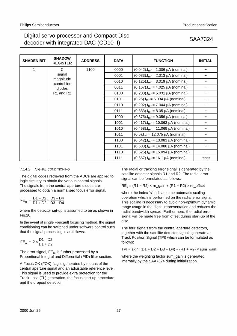
1 Csignal
magnitudecontrol for
diodesR1 and R2
1100 0000 (0.042).Iref = 1.006 µA (nominal) −0001 (0.083).Iref = 2.013 µA (nominal) −0010 (0.125).Iref = 3.019 µA (nominal) −0011 (0.167).Iref = 4.025 µA (nominal) −0100 (0.208).Iref = 5.031 µA (nominal) −0101 (0.25).Iref = 6.034 µA (nominal) −0110 (0.292).Iref = 7.044 µA (nominal) −0111 (0.333).Iref = 8.05 µA (nominal) −1000 (0.375).Iref = 9.056 µA (nominal) −1001 (0.417).Iref = 10.063 µA (nominal) −1010 (0.458).Iref = 11.069 µA (nominal) −1011 (0.5).Iref = 12.075 µA (nominal) −1100 (0.542).Iref = 13.081 µA (nominal) −1101 (0.583).Iref = 14.088 µA (nominal) −1110 (0.625).Iref = 15.094 µA (nominal) −1111 (0.667).Iref = 16.1 µA (nominal) reset
SHADEN BITSHADOW
REGISTERADDRESS DATA FUNCTION INITIAL
7.14.2 SIGNAL CONDITIONING
The digital codes retrieved from the ADCs are applied tologic circuitry to obtain the various control signals.The signals from the central aperture diodes areprocessed to obtain a normalised focus error signal.
where the detector set-up is assumed to be as shown inFig.20.
In the event of single Foucault focusing method, the signalconditioning can be switched under software control suchthat the signal processing is as follows:
The error signal, FEn, is further processed by aProportional Integral and Differential (PID) filter section.
A Focus OK (FOK) flag is generated by means of thecentral aperture signal and an adjustable reference level.This signal is used to provide extra protection for theTrack-Loss (TL) generation, the focus start-up procedureand the dropout detection.
The radial or tracking error signal is generated by thesatellite detector signals R1 and R2. The radial errorsignal can be formulated as follows:
REs = (R1 − R2) × re_gain + (R1 + R2) × re_offset
where the index ‘s’ indicates the automatic scalingoperation which is performed on the radial error signal.This scaling is necessary to avoid non-optimum dynamicrange usage in the digital representation and reduces theradial bandwidth spread. Furthermore, the radial errorsignal will be made free from offset during start-up of thedisc.
The four signals from the central aperture detectors,together with the satellite detector signals generate aTrack Position Signal (TPI) which can be formulated asfollows:
TPI = sign [(D1 + D2 + D3 + D4) − (R1 + R2) × sum_gain]
where the weighting factor sum_gain is generatedinternally by the SAA7324 during initialization.
FEnD1 D2–D1 D2+---------------------
D3 D4–D3 D4+---------------------–=
FEn 2D1 D2–D1 D2+---------------------×=
2000 Jun 26 28
Philips Semiconductors Product specification
Digital servo processor and Compact Discdecoder with integrated DAC (CD10 II)
SAA7324
handbook, full pagewidth
D3
D1
D2
SATELLITEDIODE R1
SATELLITEDIODE R2
D1
D3
D2
D4
SATELLITEDIODE R1
SATELLITEDIODE R2
D1
D2
D3
D4
SATELLITEDIODE R1
SATELLITEDIODE R2
single Foucault astigmatic focus double Foucault
MBG422
Fig.20 Detector arrangement.
7.14.3 FOCUS SERVO SYSTEM
7.14.3.1 Focus start-up
Five initially loaded coefficients influence the start-upbehaviour of the focus controller. The automaticallygenerated triangular voltage can be influenced by3 parameters; for height (ramp_height) and DC offset(ramp_offset) of the triangle and its steepness(ramp_incr).
For protection against false focus point detections twoparameters are available which are an absolute level onthe CA signal (CA_start) and a level on the FEn signal(FE_start). When this CA level is reached the FOK signalbecomes true.
If the FOK signal is true and the level on the FEn signal isreached, the focus PID is enabled to switch-on when thenext zero crossing is detected in the FEn signal.
7.14.3.2 Focus position control loop
The focus control loop contains a digital PID controllerwhich has 5 parameters that are available to the user.These coefficients influence the integrating (foc_int),proportional (foc_lead_length, part of foc_parm3) anddifferentiating (foc_pole_lead, part of foc_parm1) action ofthe PID and a digital low-pass filter (foc_pole_noise, partof foc_parm2) following the PID. The fifth coefficientfoc_gain influences the loop gain.
7.14.3.3 Dropout detection
This detector can be influenced by one parameter(CA_drop). The FOK signal will become false and theintegrator of the PID will hold if the CA signal drops belowthis programmable absolute CA level. When the FOKsignal becomes false it is assumed, initially, to be causedby a black dot.
2000 Jun 26 29
Philips Semiconductors Product specification
Digital servo processor and Compact Discdecoder with integrated DAC (CD10 II)
SAA7324
7.14.3.4 Focus loss detection and fast restart
Whenever FOK is false for longer than approximately3 ms, it is assumed that the focus point is lost. A fastrestart procedure is initiated which is capable of restartingthe focus loop within 200 to 300 ms depending on theprogrammed coefficients of the microcontroller.
7.14.3.5 Focus loop gain switching
The gain of the focus control loop (foc_gain) can bemultiplied by a factor of 2 or divided by a factor of 2 duringnormal operation. The integrator value of the PID iscorrected accordingly. The differentiating (foc_pole_lead)action of the PID can be switched at the same time as thegain switching is performed.
7.14.3.6 Focus automatic gain control loop
The loop gain of the focus control loop can be correctedautomatically to eliminate tolerances in the focus loop.This gain control injects a signal into the loop which is usedto correct the loop gain. Since this decreases the optimumperformance, the gain control should only be activated fora short time (for example, when starting a new disc).
7.14.4 RADIAL SERVO SYSTEM
7.14.4.1 Level initialization
During start-up an automatic adjustment procedure isactivated to set the values of the radial error gain (re_gain),offset (re_offset) and satellite sum gain (sum_gain) for TPIlevel generation. The initialization procedure runs in aradial open loop situation and is ≤300 ms. This start-uptime period may coincide with the last part of the motorstart-up time period:
• Automatic gain adjustment: as a result of thisinitialization the amplitude of the RE signal is adjusted towithin ±10% around the nominal RE amplitude
• Offset adjustment: the additional offset in RE due to thelimited accuracy of the start-up procedure is less than±50 nm
• TPI level generation: the accuracy of the initializationprocedure is such that the duty factor range of TPIbecomes 0.4 < duty factor < 0.6 (default dutyfactor = TPI HIGH/TPI period).
7.14.4.2 Sledge control
The microcontroller can move the sledge in both directionsvia the steer sledge command.
7.14.4.3 Tracking control
The actuator is controlled using a PID loop filter with userdefined coefficients and gain. For stable operationbetween the tracks, the S-curve is extended over 0.75 ofthe track. On request from the microcontroller, S-curveextension over 2.25 tracks is used, automatically changingto access control when exceeding those 2.25 tracks.
Both modes of S-curve extension make use of atrack-count mechanism. In this mode, track countingresults in an ‘automatic return-to-zero track’, to avoidmajor music rhythm disturbances in the audio output forimproved shock resistance. The sledge is continuouslycontrolled, or provided with step pulses to reduce powerconsumption using the filtered value of the radial PIDoutput. Alternatively, the microcontroller can read theaverage voltage on the radial actuator and provide thesledge with step pulses to reduce power consumption.Filter coefficients of the continuous sledge control can bepreset by the user.
7.14.4.4 Access
The access procedure is divided into two different modes(see Table 13), depending on the requested jump size.
Table 13 Access modes
Note
1. Microcontroller presettable.
The access procedure makes use of a track countingmechanism, a velocity signal based on a fixed number oftracks passed within a fixed time interval, a velocity setpoint calculated from the number of tracks to go and a userprogrammable parameter indicating the maximum sledgeperformance.
If the number of tracks remaining is greater than thebrake_distance then the sledge jump mode should beactivated or, the actuator jump should be performed.The requested jump size together with the required sledgebreaking distance at maximum access speed defines thebrake_distance value.
ACCESSTYPE
JUMP SIZE(1) ACCESSSPEED
Actuator jump 1 - brake_distance decreasingvelocity
Sledge jump brake_distance - 32768 maximumpower tosledge(1)
2000 Jun 26 30
Philips Semiconductors Product specification
Digital servo processor and Compact Discdecoder with integrated DAC (CD10 II)
SAA7324
During the actuator jump mode, velocity control with aPI controller is used for the actuator. The sledge is thencontinuously controlled using the filtered value of the radialPID output. All filter parameters (for actuator and sledge)are user programmable.
In the sledge jump mode maximum power (userprogrammable) is applied to the sledge in the correctdirection while the actuator becomes idle (the contents ofthe actuator integrator leaks to zero just after the sledgejump mode is initiated). The actuator can be electronicallydamped during sledge jump. The gain of the damping loopis controlled via the hold_mult parameter.
The fast track jumping circuitry can be enabled/disabledvia the xtra_preset parameter.
7.14.4.5 Radial automatic gain control loop
The loop gain of the radial control loop can be correctedautomatically to eliminate tolerances in the radial loop.This gain control injects a signal into the loop which is usedto correct the loop gain. Since this decreases the optimumperformance, the gain control should only be activated fora short time (for example, when starting a new disc).
This gain control differs from the level initialization. Thelevel initialization should be performed first.The disadvantage of using the level initialization withoutthe gain control is that only tolerances from the front-endare reduced.
7.14.5 OFF-TRACK COUNTING
The Track Position Signal (TPI) is a flag which is used toindicate whether the radial spot is positioned on the track,with a margin of ±1⁄4 of the track-pitch. In combination withthe Radial Polarity flag (RP) the relative spot position overthe tracks can be determined.
These signals are, however, afflicted with someuncertainties caused by:
• Disc defects such as scratches and fingerprints
• The HF information on the disc, which is considered asnoise by the detector signals.
In order to determine the spot position with sufficientaccuracy, extra conditions are necessary to generate aTrack Loss signal (TL) and an off-track counter value.These extra conditions influence the maximum speed andthis implies that, internally, one of the following threecounting states is selected:
1. Protected state: used in normal play situations. A goodprotection against false detection caused by discdefects is important in this state.
2. Slow counting state: used in low velocity track jumpsituations. In this state a fast response is importantrather than the protection against disc defects (if thephase relationship between TL and RP of 1⁄2π radiansis affected too much, the direction cannot then bedetermined accurately).
3. Fast counting state: used in high velocity track jumpsituations. Highest obtainable velocity is the mostimportant feature in this state.
7.14.6 DEFECT DETECTION
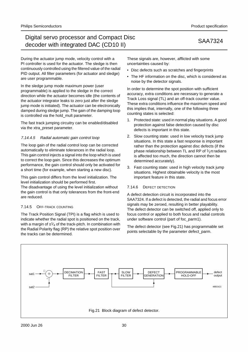
A defect detection circuit is incorporated into theSAA7324. If a defect is detected, the radial and focus errorsignals may be zeroed, resulting in better playability.The defect detector can be switched off, applied only tofocus control or applied to both focus and radial controlsunder software control (part of foc_parm1).
The defect detector (see Fig.21) has programmable setpoints selectable by the parameter defect_parm.
handbook, full pagewidth
DECIMATIONFILTER
FASTFILTER
DEFECTGENERATION
PROGRAMMABLEHOLD-OFF
SLOWFILTER
defectoutputsat1
sat2
+
−
MBG421
Fig.21 Block diagram of defect detector.
2000 Jun 26 31
Philips Semiconductors Product specification
Digital servo processor and Compact Discdecoder with integrated DAC (CD10 II)
SAA7324
7.14.7 OFF-TRACK DETECTION
During active radial tracking, off-track detection has beenrealised by continuously monitoring the off-track countervalue. The off-track flag becomes valid whenever theoff-track counter value is not equal to zero. Depending onthe type of extended S-curve, the off-track counter is resetafter 0.75 extend or at the original track in the 2.25 trackextend mode.
7.14.8 HIGH-LEVEL FEATURES
7.14.8.1 Interrupt mechanism and STATUS pin
The STATUS pin is an output which is active LOW, itsoutput is selected by decoder register 7 to be either thedecoder status bit (active LOW) selected by decoderregister 2 (only available in 4-wire bus mode) or theinterrupt signal generated by the servo part.
Eight signals from the interrupt status register areselectable from the servo part via the interrupt_maskparameter. The interrupt is reset by sending the readhigh-level status command. The 8 signals are as follows:
• Focus lost: dropout of longer than 3 ms
• Subcode ready
• Subcode absolute seconds changed
• Subcode discontinuity detected: new subcode timebefore previous subcode time, or more than 10 frameslater than previous subcode time
• Radial error: during radial on-track, no new subcodeframe occurs within time defined by the ‘playwatchtime’parameter; during radial jump, less than 4 tracks havebeen crossed during time defined by the‘jumpwatchtime’ parameter
• Autosequencer state change
• Autosequencer error
• Subcode interface blocked: the internal decoderinterface is being used.
It should be noted that if the STATUS pin output is selectedvia decoder register 2 and either the microcontroller writesa different value to decoder register 2 or the decoderinterface is enabled then the STATUS output will change.
7.14.8.2 Decoder interface
The decoder interface allows decoder registers 0 to F tobe programmed and subcode Q-channel data to be readvia servo commands. The interface is enabled/disabled bythe preset latch command (and the xtra_presetparameter).
7.14.8.3 Automatic error handling
Three Watchdogs are present:
• Focus: detects focus dropout of longer than 3 ms, setsfocus lost interrupt, switches off radial and sledgeservos, disables drive to disc motor
• Radial play: started when radial servo is in on-trackmode and a first subcode frame is found; detects whenmaximum time between two subcode frames exceedsthe time set by playwatchtime parameter; then setsradial error interrupt, switches radial and sledge servosoff, puts disc motor in jump mode
• Radial jump: active when radial servo is in long jump orshort jump modes; detects when the off-track countervalue decreases by less than 4 tracks between tworeadings (time interval set by jumpwatchtimeparameter); then sets radial jump error, switches radialand sledge servos off to cancel jump.
The focus Watchdog is always active, the radialWatchdogs are selectable via the radcontrol parameter.
7.14.8.4 Automatic sequencers and timer interrupts
Two automatic sequencers are implemented (and must beinitialized after power-on):
• Autostart sequencer: controls the start-up of focus,radial and motor
• Autostop sequencer: brakes the disc and shuts downservos.
When the automatic sequencers are not used it is possibleto generate timer interrupts, defined by thetime_parameter coefficient.
7.14.8.5 High-level status
The read high-level status command can be used to obtainthe interrupt, decoder, autosequencer status registers andthe motor start time. Use of the read high-level statuscommand clears the interrupt status register, andre-enables the subcode read via a servo command.
7.14.9 DRIVER INTERFACE
The control signals (pins RA, FO and SL) for themechanism actuators are pulse density modulated.The modulating frequency can be set to either1.0584 (DSD mode) or 2.1168 MHz; controlled via thextra_preset parameter. An analog representation of theoutput signals can be achieved by connecting a 1st-orderlow-pass filter to the outputs.
2000 Jun 26 32
Philips Semiconductors Product specification
Digital servo processor and Compact Discdecoder with integrated DAC (CD10 II)
SAA7324
During reset (i.e. RESET pin is held LOW) theRA, FO and SL pins are high-impedance.
7.14.10 LASER INTERFACE
The LDON pin (open-drain output) is used to switch thelaser off and on. When the laser is on, the output ishigh-impedance. The action of the LDON pin is controlledby the xtra_preset parameter; the pin is automaticallydriven if the focus control loop is active.
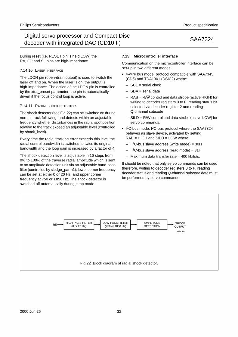
7.14.11 RADIAL SHOCK DETECTOR
The shock detector (see Fig.22) can be switched on duringnormal track following, and detects within an adjustablefrequency whether disturbances in the radial spot positionrelative to the track exceed an adjustable level (controlledby shock_level).
Every time the radial tracking error exceeds this level theradial control bandwidth is switched to twice its originalbandwidth and the loop gain is increased by a factor of 4.
The shock detection level is adjustable in 16 steps from0% to 100% of the traverse radial amplitude which is sentto an amplitude detection unit via an adjustable band-passfilter (controlled by sledge_parm1); lower corner frequencycan be set at either 0 or 20 Hz, and upper cornerfrequency at 750 or 1850 Hz. The shock detector isswitched off automatically during jump mode.
7.15 Microcontroller interface
Communication on the microcontroller interface can beset-up in two different modes:
• 4-wire bus mode: protocol compatible with SAA7345(CD6) and TDA1301 (DSIC2) where:
– SCL = serial clock
– SDA = serial data
– RAB = R/W control and data strobe (active HIGH) forwriting to decoder registers 0 to F, reading status bitselected via decoder register 2 and readingQ-channel subcode
– SILD = R/W control and data strobe (active LOW) forservo commands.
• I2C-bus mode: I2C-bus protocol where the SAA7324behaves as slave device, activated by settingRAB = HIGH and SILD = LOW where:
– I2C-bus slave address (write mode) = 30H
– I2C-bus slave address (read mode) = 31H
– Maximum data transfer rate = 400 kbits/s.
It should be noted that only servo commands can be usedtherefore, writing to decoder registers 0 to F, readingdecoder status and reading Q-channel subcode data mustbe performed by servo commands.
handbook, full pagewidthRE
MGC914
SHOCKOUTPUT
HIGH-PASS FILTER(0 or 20 Hz)
LOW-PASS FILTER(750 or 1850 Hz)
AMPLITUDEDETECTION
Fig.22 Block diagram of radial shock detector.
2000 Jun 26 33
Philips Semiconductors Product specification
Digital servo processor and Compact Discdecoder with integrated DAC (CD10 II)
SAA7324
7.15.1 MICROCONTROLLER INTERFACE (4-WIRE BUS MODE)
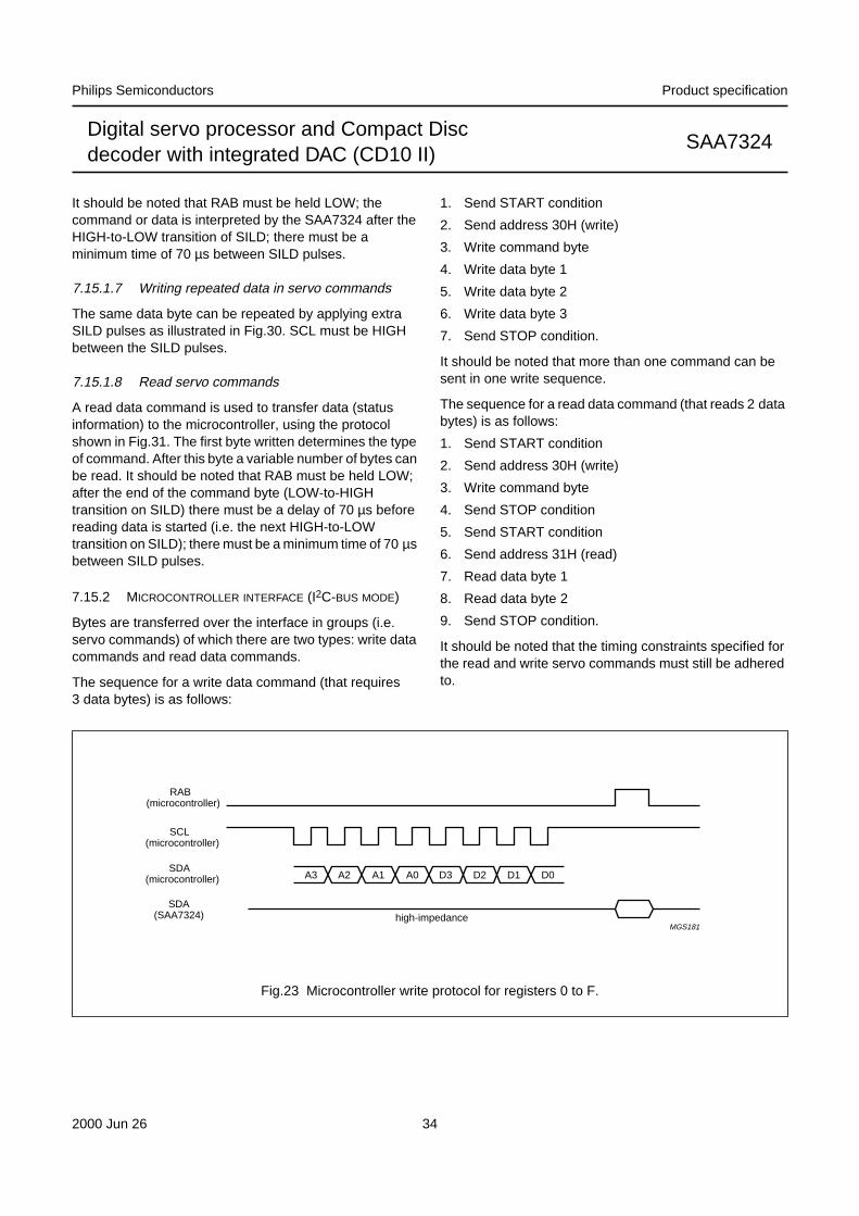
7.15.1.1 Writing data to registers 0 to F
The sixteen 4-bit programmable configuration registers,0 to F (see Table 14), can be written to via themicrocontroller interface using the protocol shown inFig.23.
It should be noted that SILD must be held HIGH; A3 to A0identifies the register number and D3 to D0 is the data.The data is latched into the register on the LOW-to-HIGHtransition of RAB.
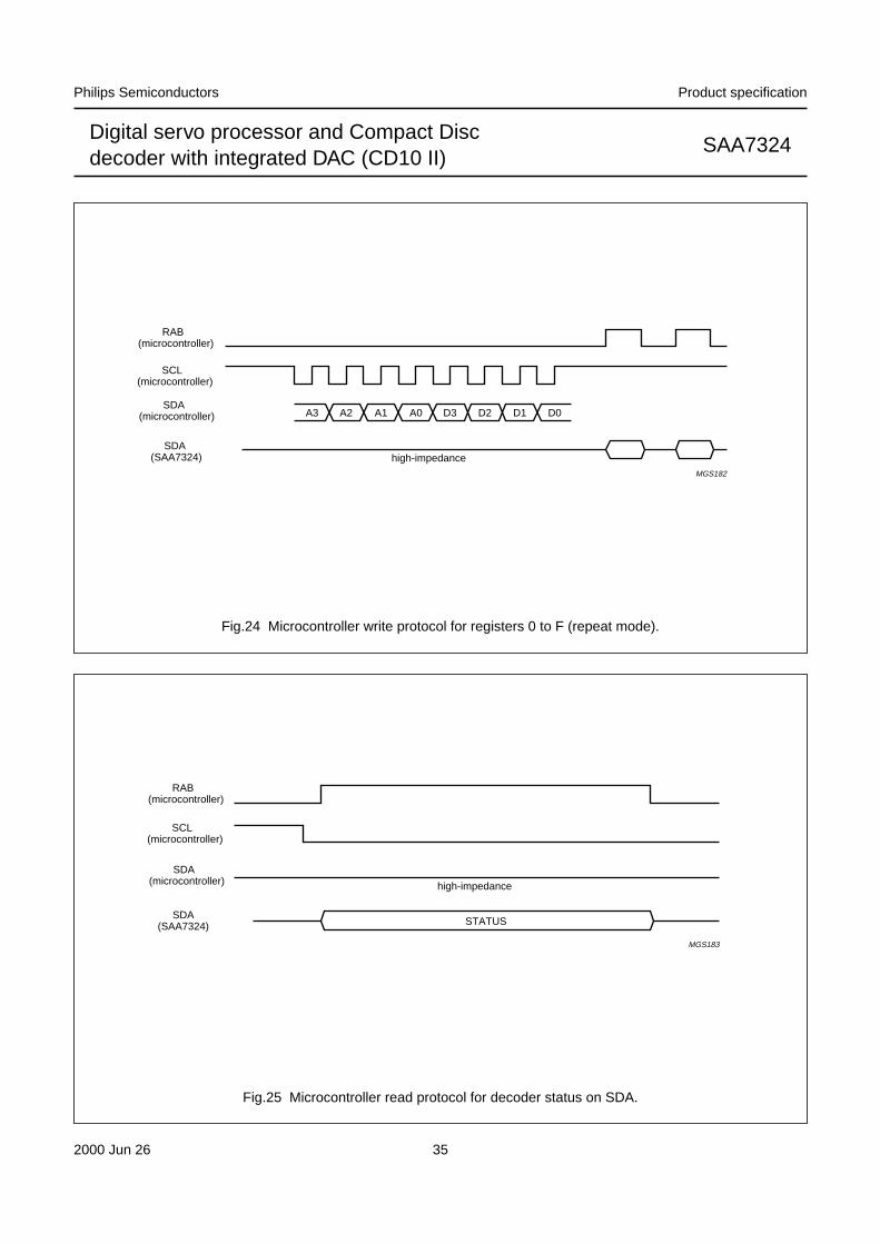
7.15.1.2 Writing repeated data to registers 0 to F
The same data can be repeated several times (e.g. for afade function) by applying extra RAB pulses as shown inFig.24. It should be noted that SCL must stay HIGHbetween RAB pulses.
7.15.1.3 Reading decoder status information on SDA
There are several internal status signals, selected viaregister 2, which can be made available on the SDA line:
SUBQREADY-I: LOW if new subcode word is ready inQ-channel register
MOTSTART1: HIGH if motor is turning at 75% or moreof nominal speed
MOTSTART2: HIGH if motor is turning at 50% or moreof nominal speed
MOTSTOP: HIGH if motor is turning at 12% or less ofnominal speed; can be set to indicate 6% or less(instead of 12% or less) via register E
PLL lock: HIGH if sync coincidence signals are found
V1: follows input on pin V1
V2: follows input on pin V2
MOTOR-OV: HIGH if the motor servo output stagesaturates
FIFO-OV: HIGH if FIFO overflows
SHOCK: MOTSTART2 + PLL Lock + MOTOR-OV +FIFO-OV + servo interrupt signal + OTD (HIGH if shockdetected)
LA-SHOCK: latched SHOCK signal.
The status read protocol is shown in Fig.25. It should benoted that SILD must be held HIGH.
7.15.1.4 Reading Q-channel subcode
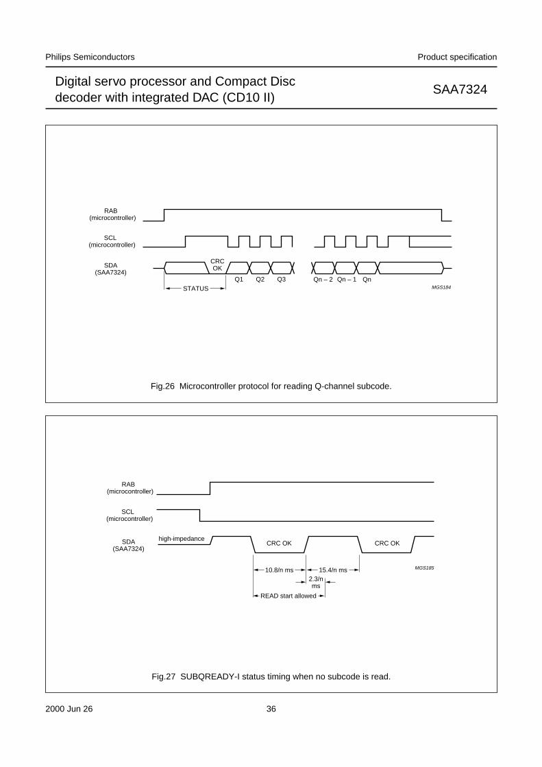
To read the Q-channel subcode direct in the 4-wire busmode, the SUBQREADY-I signal should be selected asstatus signal. The subcode read protocol is illustrated inFig.26.
It should be noted that SILD must be held HIGH; aftersubcode read starts, the microcontroller may take as longas it wants to terminate the read operation. When enoughsubcode has been read (1 to 96 bits), terminate reading bypulling RAB LOW.
Alternatively, the Q-channel subcode can be read using aservo command as follows:
• Use the read high-level status command to monitor thesubcode ready signal
• Send the read subcode command and read the requirednumber of bytes (up to 12)
• Send the read high-level status command; to re-enablethe decoder interface.
7.15.1.5 Behaviour of the SUBQREADY-I signal
When the CRC of the Q-channel word is good, and nosubcode is being read, the SUBQREADY-I status signalwill react as shown in Fig.27. When the CRC is good andthe subcode is being read, the timing in Fig.28 applies.
If t1 (SUBQREADY-I status LOW to end of subcode read)is below 2.6/n ms, then t2 = 13.1/n ms (i.e. themicrocontroller can read all subcode frames if it completesthe read operation within 2.6/n ms after the subcode isready). If these criteria are not met, it is only possible toguarantee that t3 will be below 26.2/n ms (approximately).
If subcode frames with failed CRCs are present, thet2 and t3 times will be increased by 13.1/n ms for eachdefective subcode frame.
It should be noted that in the lock-to-disc mode ‘n’ isreplaced by ‘d’, which is the disc speed factor.
7.15.1.6 Write servo commands
A write data command is used to transfer data (a numberof bytes) from the microcontroller, using the protocolshown in Fig.29. The first of these bytes is the commandbyte and the following are data bytes; the number(between 1 and 7) depends on the command byte.
2000 Jun 26 34
Philips Semiconductors Product specification
Digital servo processor and Compact Discdecoder with integrated DAC (CD10 II)
SAA7324
It should be noted that RAB must be held LOW; thecommand or data is interpreted by the SAA7324 after theHIGH-to-LOW transition of SILD; there must be aminimum time of 70 µs between SILD pulses.
7.15.1.7 Writing repeated data in servo commands
The same data byte can be repeated by applying extraSILD pulses as illustrated in Fig.30. SCL must be HIGHbetween the SILD pulses.
7.15.1.8 Read servo commands
A read data command is used to transfer data (statusinformation) to the microcontroller, using the protocolshown in Fig.31. The first byte written determines the typeof command. After this byte a variable number of bytes canbe read. It should be noted that RAB must be held LOW;after the end of the command byte (LOW-to-HIGHtransition on SILD) there must be a delay of 70 µs beforereading data is started (i.e. the next HIGH-to-LOWtransition on SILD); there must be a minimum time of 70 µsbetween SILD pulses.
7.15.2 MICROCONTROLLER INTERFACE (I2C-BUS MODE)
Bytes are transferred over the interface in groups (i.e.servo commands) of which there are two types: write datacommands and read data commands.
The sequence for a write data command (that requires3 data bytes) is as follows:
1. Send START condition
2. Send address 30H (write)
3. Write command byte
4. Write data byte 1
5. Write data byte 2
6. Write data byte 3
7. Send STOP condition.
It should be noted that more than one command can besent in one write sequence.
The sequence for a read data command (that reads 2 databytes) is as follows:
1. Send START condition
2. Send address 30H (write)
3. Write command byte
4. Send STOP condition
5. Send START condition
6. Send address 31H (read)
7. Read data byte 1
8. Read data byte 2
9. Send STOP condition.
It should be noted that the timing constraints specified forthe read and write servo commands must still be adheredto.
A3 A2 A1 A0 D3 D2 D1 D0
SDA(SAA7324)
SCL (microcontroller)
RAB (microcontroller)
SDA (microcontroller)
MGS181high-impedance
Fig.23 Microcontroller write protocol for registers 0 to F.
2000 Jun 26 35
Philips Semiconductors Product specification
Digital servo processor and Compact Discdecoder with integrated DAC (CD10 II)
SAA7324
A3 A2 A1 A0 D3 D2 D1 D0
SDA (SAA7324)
MGS182
SCL (microcontroller)
RAB (microcontroller)
SDA (microcontroller)
high-impedance
Fig.24 Microcontroller write protocol for registers 0 to F (repeat mode).
SDA(SAA7324)
MGS183
STATUS
SCL (microcontroller)
RAB (microcontroller)
SDA (microcontroller) high-impedance
Fig.25 Microcontroller read protocol for decoder status on SDA.
2000 Jun 26 36
Philips Semiconductors Product specification
Digital servo processor and Compact Discdecoder with integrated DAC (CD10 II)
SAA7324
Q1 Q2 Q3 Qn – 1
SDA(SAA7324)
MGS184
Qn – 2 QnSTATUS
CRCOK
SCL (microcontroller)
RAB (microcontroller)
Fig.26 Microcontroller protocol for reading Q-channel subcode.
SDA(SAA7324)
10.8/n ms 15.4/n ms2.3/nms
READ start allowed
high-impedanceCRC OK CRC OK
MGS185
SCL (microcontroller)
RAB (microcontroller)
Fig.27 SUBQREADY-I status timing when no subcode is read.
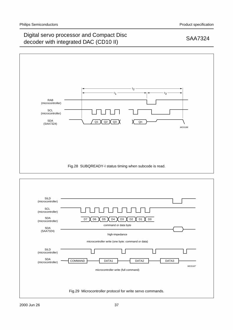
2000 Jun 26 37
Philips Semiconductors Product specification
Digital servo processor and Compact Discdecoder with integrated DAC (CD10 II)
SAA7324
Q1 Q2 Q3 QnSDA(SAA7324)
t2t1 t3
MGS186
SCL (microcontroller)
RAB (microcontroller)
Fig.28 SUBQREADY-I status timing when subcode is read.
handbook, full pagewidth
D7 D6 D5 D4 D3 D2 D1 D0
SDA(SAA7324)
SILD(microcontroller)
SCL (microcontroller)
SDA(microcontroller)
SILD(microcontroller)
SDA(microcontroller) COMMAND DATA1 DATA2 DATA3
command or data byte
high-impedance
microcontroller write (one byte: command or data)
microcontroller write (full command)MGS187
Fig.29 Microcontroller protocol for write servo commands.
2000 Jun 26 38
Philips Semiconductors Product specification
Digital servo processor and Compact Discdecoder with integrated DAC (CD10 II)
SAA7324
handbook, full pagewidth
SILD(microcontroller)
SDA(microcontroller)
microcontroller write (full command)
COMMAND DATA1
MBG413
Fig.30 Microcontroller protocol for repeated data in write servo commands.
handbook, full pagewidth
DATA1 DATA2 DATA3
COMMAND
SILD(microcontroller)
SILD(microcontroller)
SCL(microcontroller)
SDA(microcontroller)
SDA (SAA7324)
SDA (SAA7324) D7 D6 D5 D4 D3 D2 D1 D0
data byte
microcontroller read (one data byte)
microcontroller read (full command)MGS188
Fig.31 Microcontroller protocol for read servo commands.
2000 Jun 26 39
Philips Semiconductors Product specification
Digital servo processor and Compact Discdecoder with integrated DAC (CD10 II)
SAA7324
7.15.3 DECODER REGISTERS AND SHADOW REGISTERS
To maintain compatibility with the SAA737x series,decoder registers 0 to F are identical to the SAA7370.However, to control the extra functionality of SAA7324, anew set of registers called shadow registers have beenimplemented.
These are accessed by using the LSB of decoderregister F. This bit is called SHADEN (shadow registersenable) on SAA7324. When this bit is set to logic 1(i.e. decoder register F set to XXX1), any subsequentaddresses will be decoded by the shadow registers.In fact, only four addresses are implemented as shadowregisters; 3, 7, A and C. Any other addresses sent whileSHADEN = 1 are invalid and have no effect.
When SHADEN is set to logic 0 (decoder register F set toXXX0) all subsequent addresses are decoded by the maindecoder registers again.
Access to decoder register F is always enabled so thatSHADEN can be set or reset as required.
The SHADEN bit and subsequent shadow registers areprogrammed identically to the main decoder registers,i.e. they can be directly programmed when using theSAA7324 in 4-wire mode or programmed via the servointerface when using 3-wire or I2C-bus modes.
The main decoder registers are given in Table 14.The functions implemented using shadow registers aregiven in Table 16.
7.15.4 SUMMARY OF FUNCTIONS CONTROLLED BY DECODER REGISTERS 0 TO F
Table 14 Registers 0 to F
REGISTER ADDRESS DATA FUNCTION INITIAL (1)
0(fade andattenuation)
0000 0000 mute reset
0010 attenuate −0001 full-scale −0100 step down −0101 step up −
1(motor mode)
0001 X000 motor off mode reset
X 001 motor stop mode 1 −X010 motor stop mode 2 −X011 motor start mode 1 −X100 motor start mode 2 −X101 motor jump mode −X111 motor play mode −X110 motor jump mode 1 −1XXX anti-windup active −0XXX anti-windup off reset
2000 Jun 26 40
Philips Semiconductors Product specification
Digital servo processor and Compact Discdecoder with integrated DAC (CD10 II)
SAA7324
2(status controlto servo part -not theSTATUS pin)
0010 0000 status = SUBQREADY-I reset
0001 status = MOTSTART1 −0010 status = MOTSTART2 −0011 status = MOTSTOP −0100 status = PLL lock −0101 status = V1 −0110 status = V2 −0111 status = MOTOR-OV −1000 status = FIFO overflow −1001 status = shock detect −1010 status = latched shock detect −1011 status = latched shock detect reset −
3(DAC output)
0011 1010 I2S-bus; CD-ROM mode −1011 EIAJ; CD-ROM mode −1100 I2S-bus; 18-bit; 4fs mode reset
1111 I2S-bus; 18-bit; 2fs mode −1110 I2S-bus; 16-bit; fs mode −0000 EIAJ; 16-bit; 4fs −0011 EIAJ; 16-bit; 2fs −0010 EIAJ; 16-bit; fs −0100 EIAJ; 18-bit; 4fs −0111 EIAJ; 18-bit; 2fs −0110 EIAJ; 18-bit; fs −
4(motor gain)
0100 X000 motor gain G = 3.2 reset
X001 motor gain G = 4.0 −X010 motor gain G = 6.4 −X011 motor gain G = 8.0 −X100 motor gain G = 12.8 −X101 motor gain G = 16.0 −X110 motor gain G = 25.6 −X111 motor gain G = 32.0 −0XXX disable comparator clock divider reset
1XXX enable comparator clock divider; only if SELLPLLset HIGH
−
5(motorbandwidth)
0101 XX00 motor f4 = 0.5 × n Hz reset
XX01 motor f4 = 0.7 × n Hz −XX10 motor f4 = 1.4 × n Hz −XX11 motor f4 = 2.8 × n Hz −00XX motor f3 = 0.85 × n Hz reset
01XX motor f3 = 1.71 × n Hz −10XX motor f3 = 3.42 × n Hz −
REGISTER ADDRESS DATA FUNCTION INITIAL (1)
2000 Jun 26 41
Philips Semiconductors Product specification
Digital servo processor and Compact Discdecoder with integrated DAC (CD10 II)
SAA7324
6(motor outputconfiguration)
0110 XX00 motor power maximum 37% reset
XX01 motor power maximum 50% −XX10 motor power maximum 75% −XX11 motor power maximum 100% −00XX MOTO1, MOTO2 pins 3-state reset
01XX motor PWM mode −10XX motor PDM mode −11XX motor CDV mode −
7(DAC outputand statuscontrol)
0111 XX00 interrupt signal from servo at STATUS pin reset
XX10 status bit from decoder status register at STATUSpin
−
X0XX DAC data normal value reset
X1XX DAC data inverted value −0XXX left channel first at DAC (WCLK normal) reset
1XXX right channel first at DAC (WCLK inverted) −8(PLL loop filterbandwidth)
see Table 15 −
9(PLLequalization)
1001 0011 PLL loop filter equalization reset
0001 PLL 30 ns over-equalization −0010 PLL 15 ns over-equalization −0100 PLL 15 ns under-equalization −0101 PLL 30 ns under-equalization −
A(EBU output)
1010 XX0X EBU data before concealment −XX1X EBU data after concealment and fade reset
X0X0 level II clock accuracy (<1000 ppm) reset
X0X1 level I clock accuracy (<50 ppm) −X1X0 level III clock accuracy (>1000 ppm) −X1X1 EBU off - output low −0XXX flags in EBU off reset
1XXX flags in EBU on −B(speed control)
1011 X0XX 33.8688 MHz crystal present, or 8.4672 MHz (or16.9344 MHz) crystal with SELPLL set HIGH
reset
X1XX 16.9344 MHz crystal present −0XXX single-speed mode reset
1XXX double-speed mode −XX00 standby 1: ‘CD-STOP’ mode reset
XX10 standby 2: ‘CD-PAUSE’ mode −XX11 operating mode −
REGISTER ADDRESS DATA FUNCTION INITIAL (1)
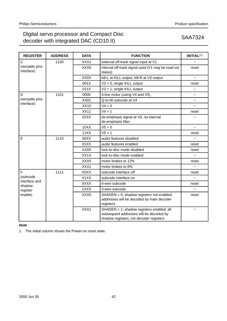
2000 Jun 26 42
Philips Semiconductors Product specification
Digital servo processor and Compact Discdecoder with integrated DAC (CD10 II)
SAA7324
Note
1. The initial column shows the Power-on reset state.
C(versatile pinsinterface)
1100 XXX1 external off-track signal input at V1 −XXX0 internal off-track signal used (V1 may be read via
status)reset
XX0X kill-L at KILL output, kill-R at V3 output −001X V3 = 0; single KILL output reset
011X V3 = 1; single KILL output −D(versatile pinsinterface)
1101 0000 4-line motor (using V4 and V5) −XX01 Q-to-W subcode at V4 −XX10 V4 = 0 −XX11 V4 = 1 reset
01XX de-emphasis signal at V5, no internalde-emphasis filter
−
10XX V5 = 0 −11XX V5 = 1 reset
E 1110 00XX audio features disabled −01XX audio features enabled reset
XX0X lock-to-disc mode disabled reset
XX1X lock-to-disc mode enabled −XXX0 motor brakes to 12% reset
XXX1 motor brakes to 6% −F(subcodeinterface andshadowregisterenable)
1111 X0XX subcode interface off reset
X1XX subcode interface on −0XXX 4-wire subcode reset
1XXX 3-wire subcode −XXX0 SHADEN = 0; shadow registers not enabled;
addresses will be decoded by main decoderregisters
reset
XXX1 SHADEN = 1; shadow registers enabled; allsubsequent addresses will be decoded byshadow registers, not decoder registers
−
REGISTER ADDRESS DATA FUNCTION INITIAL (1)
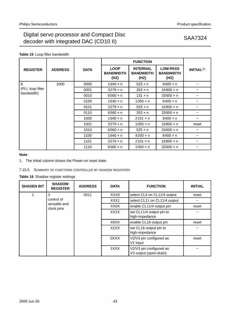
2000 Jun 26 43
Philips Semiconductors Product specification
Digital servo processor and Compact Discdecoder with integrated DAC (CD10 II)
SAA7324
Table 15 Loop filter bandwidth
Note
1. The initial column shows the Power-on reset state.
7.15.5 SUMMARY OF FUNCTIONS CONTROLLED BY SHADOW REGISTERS
Table 16 Shadow register settings
REGISTER ADDRESS DATA
FUNCTION
INITIAL (1)LOOPBANDWIDTH
(HZ)
INTERNALBANDWIDTH
(HZ)
LOW-PASSBANDWIDTH
(HZ)
8(PLL loop filterbandwidth)
1000 0000 1640 × n 525 × n 8400 × n −0001 3279 × n 263 × n 16800 × n −0010 6560 × n 131 × n 33600 × n −0100 1640 × n 1050 × n 8400 × n −0101 3279 × n 525 × n 16800 × n −0110 6560 × n 263 × n 33600 × n −1000 1640 × n 2101 × n 8400 × n −1001 3279 × n 1050 × n 16800 × n reset
1010 6560 × n 525 × n 33600 × n −1100 1640 × n 4200 × n 8400 × n −1101 3279 × n 2101 × n 16800 × n −1110 6560 × n 1050 × n 33600 × n −
SHADEN BITSHADOW
REGISTERADDRESS DATA FUNCTION INITIAL
1 3control ofversatile andclock pins
0011 XXX0 select CL4 on CL11/4 output reset
XXX1 select CL11 on CL11/4 output −XX0X enable CL11/4 output pin reset
XX1X set CL11/4 output pin tohigh-impedance
−
X0XX enable CL16 output pin reset
X1XX set CL16 output pin tohigh-impedance
−
0XXX V2/V3 pin configured asV2 input
reset
1XXX V2/V3 pin configured asV3 output (open-drain)
−
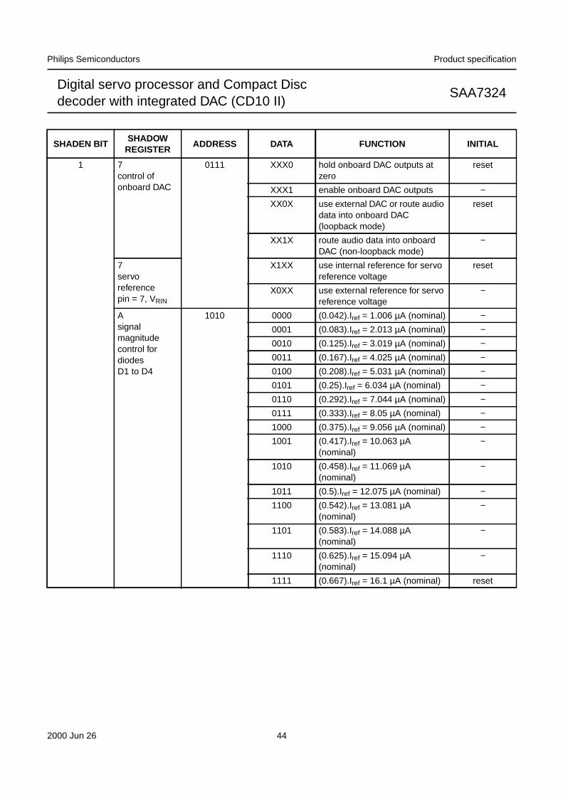
2000 Jun 26 44
Philips Semiconductors Product specification
Digital servo processor and Compact Discdecoder with integrated DAC (CD10 II)
SAA7324
1 7control ofonboard DAC
0111 XXX0 hold onboard DAC outputs atzero
reset
XXX1 enable onboard DAC outputs −XX0X use external DAC or route audio
data into onboard DAC(loopback mode)
reset
XX1X route audio data into onboardDAC (non-loopback mode)
−
7servoreferencepin = 7, VRIN
X1XX use internal reference for servoreference voltage
reset
X0XX use external reference for servoreference voltage
−
Asignalmagnitudecontrol fordiodesD1 to D4
1010 0000 (0.042).Iref = 1.006 µA (nominal) −0001 (0.083).Iref = 2.013 µA (nominal) −0010 (0.125).Iref = 3.019 µA (nominal) −0011 (0.167).Iref = 4.025 µA (nominal) −0100 (0.208).Iref = 5.031 µA (nominal) −0101 (0.25).Iref = 6.034 µA (nominal) −0110 (0.292).Iref = 7.044 µA (nominal) −0111 (0.333).Iref = 8.05 µA (nominal) −1000 (0.375).Iref = 9.056 µA (nominal) −1001 (0.417).Iref = 10.063 µA
(nominal)−
1010 (0.458).Iref = 11.069 µA(nominal)
−
1011 (0.5).Iref = 12.075 µA (nominal) −1100 (0.542).Iref = 13.081 µA
(nominal)−
1101 (0.583).Iref = 14.088 µA(nominal)
−
1110 (0.625).Iref = 15.094 µA(nominal)
−
1111 (0.667).Iref = 16.1 µA (nominal) reset
SHADEN BITSHADOW
REGISTERADDRESS DATA FUNCTION INITIAL
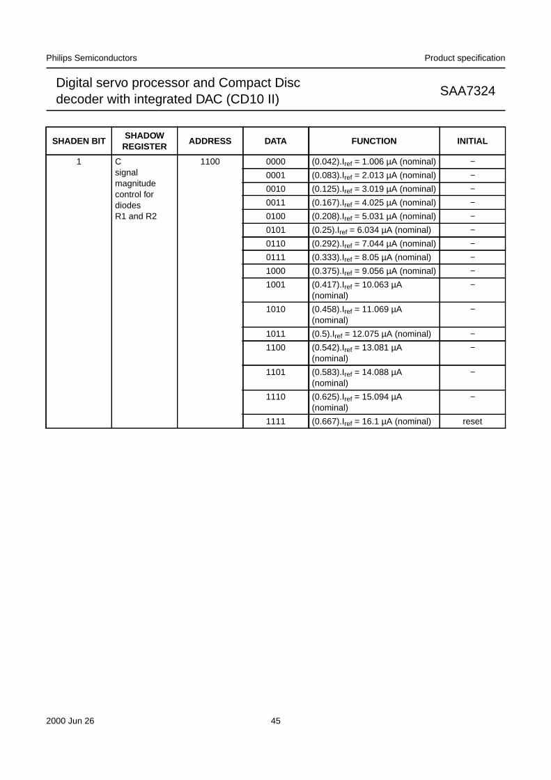
2000 Jun 26 45
Philips Semiconductors Product specification
Digital servo processor and Compact Discdecoder with integrated DAC (CD10 II)
SAA7324
1 Csignalmagnitudecontrol fordiodesR1 and R2
1100 0000 (0.042).Iref = 1.006 µA (nominal) −0001 (0.083).Iref = 2.013 µA (nominal) −0010 (0.125).Iref = 3.019 µA (nominal) −0011 (0.167).Iref = 4.025 µA (nominal) −0100 (0.208).Iref = 5.031 µA (nominal) −0101 (0.25).Iref = 6.034 µA (nominal) −0110 (0.292).Iref = 7.044 µA (nominal) −0111 (0.333).Iref = 8.05 µA (nominal) −1000 (0.375).Iref = 9.056 µA (nominal) −1001 (0.417).Iref = 10.063 µA
(nominal)−
1010 (0.458).Iref = 11.069 µA(nominal)
−
1011 (0.5).Iref = 12.075 µA (nominal) −1100 (0.542).Iref = 13.081 µA
(nominal)−
1101 (0.583).Iref = 14.088 µA(nominal)
−
1110 (0.625).Iref = 15.094 µA(nominal)
−
1111 (0.667).Iref = 16.1 µA (nominal) reset
SHADEN BITSHADOW
REGISTERADDRESS DATA FUNCTION INITIAL
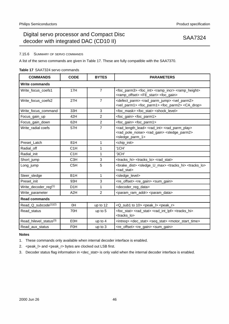
2000 Jun 26 46
Philips Semiconductors Product specification
Digital servo processor and Compact Discdecoder with integrated DAC (CD10 II)
SAA7324
7.15.6 SUMMARY OF SERVO COMMANDS
A list of the servo commands are given in Table 17. These are fully compatible with the SAA7370.
Table 17 SAA7324 servo commands
Notes
1. These commands only available when internal decoder interface is enabled.
2. <peak_l> and <peak_r> bytes are clocked out LSB first.
3. Decoder status flag information in <dec_stat> is only valid when the internal decoder interface is enabled.
COMMANDS CODE BYTES PARAMETERS
Write commands
Write_focus_coefs1 17H 7 <foc_parm3> <foc_int> <ramp_incr> <ramp_height><ramp_offset> <FE_start> <foc_gain>
Write_focus_coefs2 27H 7 <defect_parm> <rad_parm_jump> <vel_parm2><vel_parm1> <foc_parm1> <foc_parm2> <CA_drop>
Write_focus_command 33H 3 <foc_mask> <foc_stat> <shock_level>
Focus_gain_up 42H 2 <foc_gain> <foc_parm1>
Focus_gain_down 62H 2 <foc_gain> <foc_parm1>
Write_radial coefs 57H 7 <rad_length_lead> <rad_int> <rad_parm_play><rad_pole_noise> <rad_gain> <sledge_parm2><sledge_parm_1>
Preset_Latch 81H 1 <chip_init>
Radial_off C1H 1 ‘1CH’
Radial_init C1H 1 ‘3CH’
Short_jump C3H 3 <tracks_hi> <tracks_lo> <rad_stat>
Long_jump C5H 5 <brake_dist> <sledge_U_max> <tracks_hi> <tracks_lo><rad_stat>
Steer_sledge B1H 1 <sledge_level>
Preset_init 93H 3 <re_offset> <re_gain> <sum_gain>
Write_decoder_reg(1) D1H 1 <decoder_reg_data>
Write_parameter A2H 2 <param_ram_addr> <param_data>
Read commands
Read_Q_subcode(1)(2) 0H up to 12 <Q_sub1 to 10> <peak_l> <peak_r>
Read_status 70H up to 5 <foc_stat> <rad_stat> <rad_int_lpf> <tracks_hi><tracks_lo>
Read_hilevel_status(3) E0H up to 4 <intreq> <dec_stat> <seq_stat> <motor_start_time>
Read_aux_status F0H up to 3 <re_offset> <re_gain> <sum_gain>
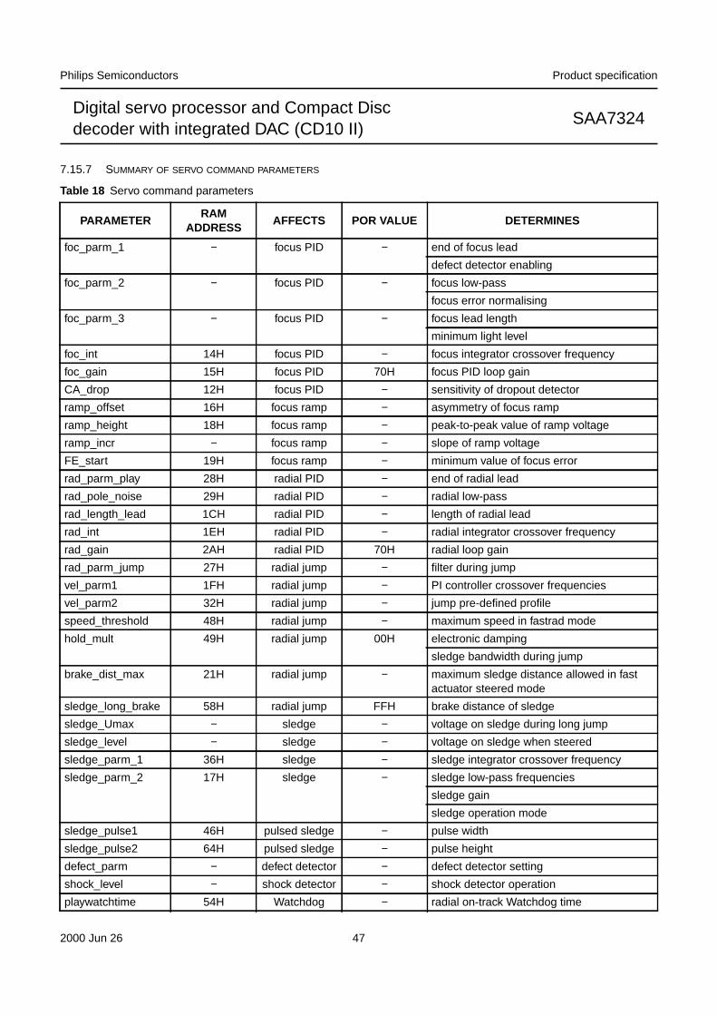
2000 Jun 26 47
Philips Semiconductors Product specification
Digital servo processor and Compact Discdecoder with integrated DAC (CD10 II)
SAA7324
7.15.7 SUMMARY OF SERVO COMMAND PARAMETERS
Table 18 Servo command parameters
PARAMETERRAM
ADDRESSAFFECTS POR VALUE DETERMINES
foc_parm_1 − focus PID − end of focus lead
defect detector enabling
foc_parm_2 − focus PID − focus low-pass
focus error normalising
foc_parm_3 − focus PID − focus lead length
minimum light level
foc_int 14H focus PID − focus integrator crossover frequency
foc_gain 15H focus PID 70H focus PID loop gain
CA_drop 12H focus PID − sensitivity of dropout detector
ramp_offset 16H focus ramp − asymmetry of focus ramp
ramp_height 18H focus ramp − peak-to-peak value of ramp voltage
ramp_incr − focus ramp − slope of ramp voltage
FE_start 19H focus ramp − minimum value of focus error
rad_parm_play 28H radial PID − end of radial lead
rad_pole_noise 29H radial PID − radial low-pass
rad_length_lead 1CH radial PID − length of radial lead
rad_int 1EH radial PID − radial integrator crossover frequency
rad_gain 2AH radial PID 70H radial loop gain
rad_parm_jump 27H radial jump − filter during jump
vel_parm1 1FH radial jump − PI controller crossover frequencies
vel_parm2 32H radial jump − jump pre-defined profile
speed_threshold 48H radial jump − maximum speed in fastrad mode
hold_mult 49H radial jump 00H electronic damping
sledge bandwidth during jump
brake_dist_max 21H radial jump − maximum sledge distance allowed in fastactuator steered mode
sledge_long_brake 58H radial jump FFH brake distance of sledge
sledge_Umax − sledge − voltage on sledge during long jump
sledge_level − sledge − voltage on sledge when steered
sledge_parm_1 36H sledge − sledge integrator crossover frequency
sledge_parm_2 17H sledge − sledge low-pass frequencies
sledge gain
sledge operation mode
sledge_pulse1 46H pulsed sledge − pulse width
sledge_pulse2 64H pulsed sledge − pulse height
defect_parm − defect detector − defect detector setting
shock_level − shock detector − shock detector operation
playwatchtime 54H Watchdog − radial on-track Watchdog time
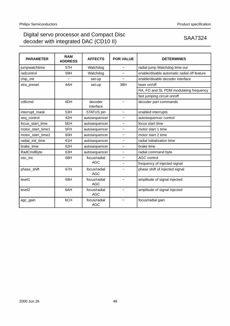
2000 Jun 26 48
Philips Semiconductors Product specification
Digital servo processor and Compact Discdecoder with integrated DAC (CD10 II)
SAA7324
jumpwatchtime 57H Watchdog − radial jump Watchdog time-out
radcontrol 59H Watchdog − enable/disable automatic radial off feature
chip_init − set-up − enable/disable decoder interface
xtra_preset 4AH set-up 38H laser on/off
RA, FO and SL PDM modulating frequency
fast jumping circuit on/off
cd6cmd 4DH decoderinterface
− decoder part commands
interrupt_mask 53H STATUS pin − enabled interrupts
seq_control 42H autosequencer − autosequencer control
focus_start_time 5EH autosequencer − focus start time
motor_start_time1 5FH autosequencer − motor start 1 time
motor_start_time2 60H autosequencer − motor start 2 time
radial_init_time 61H autosequencer − radial initialization time
brake_time 62H autosequencer − brake time
RadCmdByte 63H autosequencer − radial command byte
osc_inc 68H focus/radialAGC
− AGC control
− frequency of injected signal
phase_shift 67H focus/radialAGC
− phase shift of injected signal
level1 69H focus/radialAGC
− amplitude of signal injected
level2 6AH focus/radialAGC
− amplitude of signal injected
agc_gain 6CH focus/radialAGC
− focus/radial gain
PARAMETERRAM
ADDRESSAFFECTS POR VALUE DETERMINES
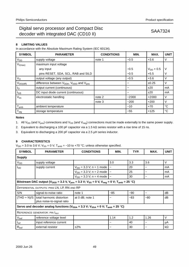
2000 Jun 26 49
Philips Semiconductors Product specification
Digital servo processor and Compact Discdecoder with integrated DAC (CD10 II)
SAA7324
8 LIMITING VALUESIn accordance with the Absolute Maximum Rating System (IEC 60134).
Notes
1. All VDD (and Vpos) connections and VSS (and Vneg) connections must be made externally to the same power supply.
2. Equivalent to discharging a 100 pF capacitor via a 1.5 kΩ series resistor with a rise time of 15 ns.
3. Equivalent to discharging a 200 pF capacitor via a 2.5 µH series inductor.
9 CHARACTERISTICSVDD = 3.0 to 3.6 V; VSS = 0 V; Tamb = −10 to +70 °C; unless otherwise specified.
SYMBOL PARAMETER CONDITIONS MIN. MAX. UNIT
VDD supply voltage note 1 −0.5 +3.6 V
VI(max) maximum input voltage
any input −0.5 VDD + 0.5 V
pins RESET, SDA, SCL, RAB and SILD −0.5 +5.5 V
VO output voltage (any output) −0.5 +3.6 V
VDD(diff) difference between VDDA, VDDD and Vpos − ±0.25 V
IO output current (continuous) − ±20 mA
II(d) DC input diode current (continuous) − ±20 mA
Ves electrostatic handling note 2 −2000 +2000 V
note 3 −200 +200 V
Tamb ambient temperature −10 +70 °CTstg storage temperature −55 +125 °C
SYMBOL PARAMETER CONDITIONS MIN. TYP. MAX. UNIT
Supply
VDD supply voltage 3.0 3.3 3.6 V
IDD supply current VDD = 3.3 V; n = 1 mode − 20 − mA
VDD = 3.3 V; n = 2 mode − 25 − mA
VDD = 3.3 V; n = 4 mode − 30 − mA
Bitstream DAC output (V DDD = 3.3 V, Vpos = 3.3 V; VSS = 0 V, Vneg = 0 V; Tamb = 25 °C)
DIFFERENTIAL OUTPUTS: PINS LN, LP, RN AND RP
S/N signal-to-noise ratio note 1 −85 −90 − dB
(THD + N)/S total harmonic distortionplus noise-to-signal ratio
at 0 dB; note 1 − −83 −80 dB
Servo and decoder analog functions (V DDA = 3.3 V; VSSA = 0 V; Tamb = 25 °C)
REFERENCE GENERATOR: PIN IREF
VIref reference voltage level 1.14 1.2 1.26 V
Iref input reference current − 40 − µA
RIref external resistor ±2% − 30 − kΩ
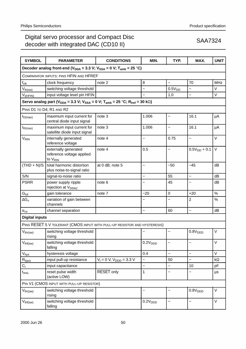
2000 Jun 26 50
Philips Semiconductors Product specification
Digital servo processor and Compact Discdecoder with integrated DAC (CD10 II)
SAA7324
Decoder analog front-end (V DDA = 3.3 V; VSSA = 0 V; Tamb = 25 °C)
COMPARATOR INPUTS: PINS HFIN AND HFREF
fclk clock frequency note 2 8 − 70 MHz
Vth(sw) switching voltage threshold − 0.5VDD − V
Vi(HFIN) input voltage level pin HFIN − 1.0 − V
Servo analog part (V DDA = 3.3 V; VSSA = 0 V; Tamb = 25 °C; RIref = 30 kΩ)
PINS D1 TO D4; R1 AND R2
ID(max) maximum input current forcentral diode input signal
note 3 1.006 − 16.1 µA
IR(max) maximum input current forsatellite diode input signal
note 3 1.006 − 16.1 µA
VRIN internally generatedreference voltage
note 4 − 0.75 − V
externally generatedreference voltage appliedto VRIN
note 4 0.5 − 0.5VDD + 0.1 V
(THD + N)/S total harmonic distortionplus noise-to-signal ratio
at 0 dB; note 5 − −50 −45 dB
S/N signal-to-noise ratio − 55 − dB
PSRR power supply ripplerejection at VDDA2
note 6 − 45 − dB
Gtol gain tolerance note 7 −20 0 +20 %
∆Gv variation of gain betweenchannels
− − 2 %
αcs channel separation − 60 − dB
Digital inputs
PINS RESET 5 V TOLERANT (CMOS INPUT WITH PULL-UP RESISTOR AND HYSTERESIS)
Vthr(sw) switching voltage thresholdrising
− − 0.8VDDD V
Vthf(sw) switching voltage thresholdfalling
0.2VDDD − − V
Vhys hysteresis voltage 0.4 − − V
Ri(pu) input pull-up resistance Vi = 0 V, VDDD = 3.3 V − 50 − kΩCi input capacitance − − 10 pF
tresL reset pulse width(active LOW)
RESET only 1 − − µs
PIN V1 (CMOS INPUT WITH PULL-UP RESISTOR)
Vthr(sw) switching voltage thresholdrising
− − 0.8VDDD V
Vthf(sw) switching voltage thresholdfalling
0.2VDDD − − V
SYMBOL PARAMETER CONDITIONS MIN. TYP. MAX. UNIT
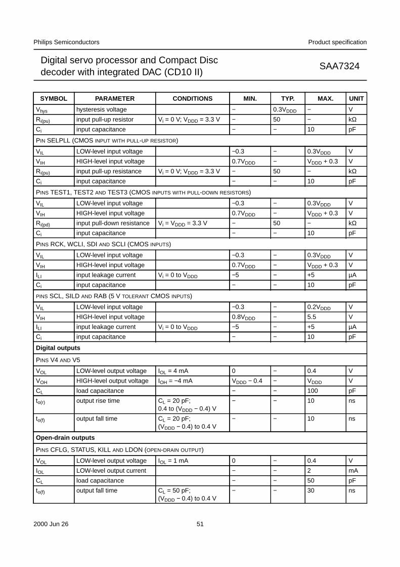
2000 Jun 26 51
Philips Semiconductors Product specification
Digital servo processor and Compact Discdecoder with integrated DAC (CD10 II)
SAA7324
Vhys hysteresis voltage − 0.3VDDD − V
Ri(pu) input pull-up resistor Vi = 0 V; VDDD = 3.3 V − 50 − kΩCi input capacitance − − 10 pF
PIN SELPLL (CMOS INPUT WITH PULL-UP RESISTOR)
VIL LOW-level input voltage −0.3 − 0.3VDDD V
VIH HIGH-level input voltage 0.7VDDD − VDDD + 0.3 V
Ri(pu) input pull-up resistance Vi = 0 V; VDDD = 3.3 V − 50 − kΩCi input capacitance − − 10 pF
PINS TEST1, TEST2 AND TEST3 (CMOS INPUTS WITH PULL-DOWN RESISTORS)
VIL LOW-level input voltage −0.3 − 0.3VDDD V
VIH HIGH-level input voltage 0.7VDDD − VDDD + 0.3 V
Ri(pd) input pull-down resistance Vi = VDDD = 3.3 V − 50 − kΩCi input capacitance − − 10 pF
PINS RCK, WCLI, SDI AND SCLI (CMOS INPUTS)
VIL LOW-level input voltage −0.3 − 0.3VDDD V
VIH HIGH-level input voltage 0.7VDDD − VDDD + 0.3 V
ILI input leakage current Vi = 0 to VDDD −5 − +5 µA
Ci input capacitance − − 10 pF
PINS SCL, SILD AND RAB (5 V TOLERANT CMOS INPUTS)
VIL LOW-level input voltage −0.3 − 0.2VDDD V
VIH HIGH-level input voltage 0.8VDDD − 5.5 V
ILI input leakage current Vi = 0 to VDDD −5 − +5 µA
Ci input capacitance − − 10 pF
Digital outputs
PINS V4 AND V5
VOL LOW-level output voltage IOL = 4 mA 0 − 0.4 V
VOH HIGH-level output voltage IOH = −4 mA VDDD − 0.4 − VDDD V
CL load capacitance − − 100 pF
to(r) output rise time CL = 20 pF;0.4 to (VDDD − 0.4) V
− − 10 ns
to(f) output fall time CL = 20 pF;(VDDD − 0.4) to 0.4 V
− − 10 ns
Open-drain outputs
PINS CFLG, STATUS, KILL AND LDON (OPEN-DRAIN OUTPUT)
VOL LOW-level output voltage IOL = 1 mA 0 − 0.4 V
IOL LOW-level output current − − 2 mA
CL load capacitance − − 50 pF
to(f) output fall time CL = 50 pF;(VDDD − 0.4) to 0.4 V
− − 30 ns
SYMBOL PARAMETER CONDITIONS MIN. TYP. MAX. UNIT
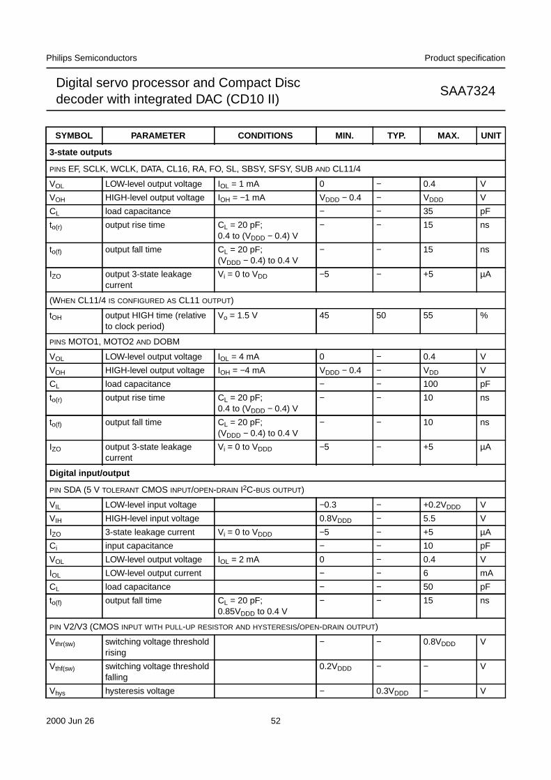
2000 Jun 26 52
Philips Semiconductors Product specification
Digital servo processor and Compact Discdecoder with integrated DAC (CD10 II)
SAA7324
3-state outputs
PINS EF, SCLK, WCLK, DATA, CL16, RA, FO, SL, SBSY, SFSY, SUB AND CL11/4
VOL LOW-level output voltage IOL = 1 mA 0 − 0.4 V
VOH HIGH-level output voltage IOH = −1 mA VDDD − 0.4 − VDDD V
CL load capacitance − − 35 pF
to(r) output rise time CL = 20 pF;0.4 to (VDDD − 0.4) V
− − 15 ns
to(f) output fall time CL = 20 pF;(VDDD − 0.4) to 0.4 V
− − 15 ns
IZO output 3-state leakagecurrent
Vi = 0 to VDD −5 − +5 µA
(WHEN CL11/4 IS CONFIGURED AS CL11 OUTPUT)
tOH output HIGH time (relativeto clock period)
Vo = 1.5 V 45 50 55 %
PINS MOTO1, MOTO2 AND DOBM
VOL LOW-level output voltage IOL = 4 mA 0 − 0.4 V
VOH HIGH-level output voltage IOH = −4 mA VDDD − 0.4 − VDD V
CL load capacitance − − 100 pF
to(r) output rise time CL = 20 pF;0.4 to (VDDD − 0.4) V
− − 10 ns
to(f) output fall time CL = 20 pF;(VDDD − 0.4) to 0.4 V
− − 10 ns
IZO output 3-state leakagecurrent
Vi = 0 to VDDD −5 − +5 µA
Digital input/output
PIN SDA (5 V TOLERANT CMOS INPUT/OPEN-DRAIN I2C-BUS OUTPUT)
VIL LOW-level input voltage −0.3 − +0.2VDDD V
VIH HIGH-level input voltage 0.8VDDD − 5.5 V
IZO 3-state leakage current Vi = 0 to VDDD −5 − +5 µA
Ci input capacitance − − 10 pF
VOL LOW-level output voltage IOL = 2 mA 0 − 0.4 V
IOL LOW-level output current − − 6 mA
CL load capacitance − − 50 pF
to(f) output fall time CL = 20 pF;0.85VDDD to 0.4 V
− − 15 ns
PIN V2/V3 (CMOS INPUT WITH PULL-UP RESISTOR AND HYSTERESIS/OPEN-DRAIN OUTPUT)
Vthr(sw) switching voltage thresholdrising
− − 0.8VDDD V
Vthf(sw) switching voltage thresholdfalling
0.2VDDD − − V
Vhys hysteresis voltage − 0.3VDDD − V
SYMBOL PARAMETER CONDITIONS MIN. TYP. MAX. UNIT
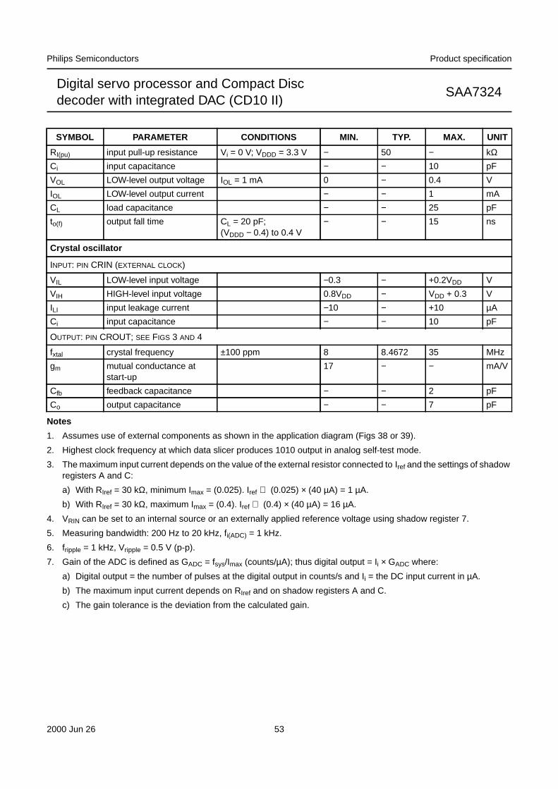
2000 Jun 26 53
Philips Semiconductors Product specification
Digital servo processor and Compact Discdecoder with integrated DAC (CD10 II)
SAA7324
Notes
1. Assumes use of external components as shown in the application diagram (Figs 38 or 39).
2. Highest clock frequency at which data slicer produces 1010 output in analog self-test mode.
3. The maximum input current depends on the value of the external resistor connected to Iref and the settings of shadowregisters A and C:
a) With RIref = 30 kΩ, minimum Imax = (0.025). Iref ⇒ (0.025) × (40 µA) = 1 µA.
b) With RIref = 30 kΩ, maximum Imax = (0.4). Iref ⇒ (0.4) × (40 µA) = 16 µA.
4. VRIN can be set to an internal source or an externally applied reference voltage using shadow register 7.
5. Measuring bandwidth: 200 Hz to 20 kHz, fi(ADC) = 1 kHz.
6. fripple = 1 kHz, Vripple = 0.5 V (p-p).
7. Gain of the ADC is defined as GADC = fsys/Imax (counts/µA); thus digital output = Ii × GADC where:
a) Digital output = the number of pulses at the digital output in counts/s and Ii = the DC input current in µA.
b) The maximum input current depends on RIref and on shadow registers A and C.
c) The gain tolerance is the deviation from the calculated gain.
RI(pu) input pull-up resistance Vi = 0 V; VDDD = 3.3 V − 50 − kΩCi input capacitance − − 10 pF
VOL LOW-level output voltage IOL = 1 mA 0 − 0.4 V
IOL LOW-level output current − − 1 mA
CL load capacitance − − 25 pF
to(f) output fall time CL = 20 pF;(VDDD − 0.4) to 0.4 V
− − 15 ns
Crystal oscillator
INPUT: PIN CRIN (EXTERNAL CLOCK)
VIL LOW-level input voltage −0.3 − +0.2VDD V
VIH HIGH-level input voltage 0.8VDD − VDD + 0.3 V
ILI input leakage current −10 − +10 µA
Ci input capacitance − − 10 pF
OUTPUT: PIN CROUT; SEE FIGS 3 AND 4
fxtal crystal frequency ±100 ppm 8 8.4672 35 MHz
gm mutual conductance atstart-up
17 − − mA/V
Cfb feedback capacitance − − 2 pF
Co output capacitance − − 7 pF
SYMBOL PARAMETER CONDITIONS MIN. TYP. MAX. UNIT
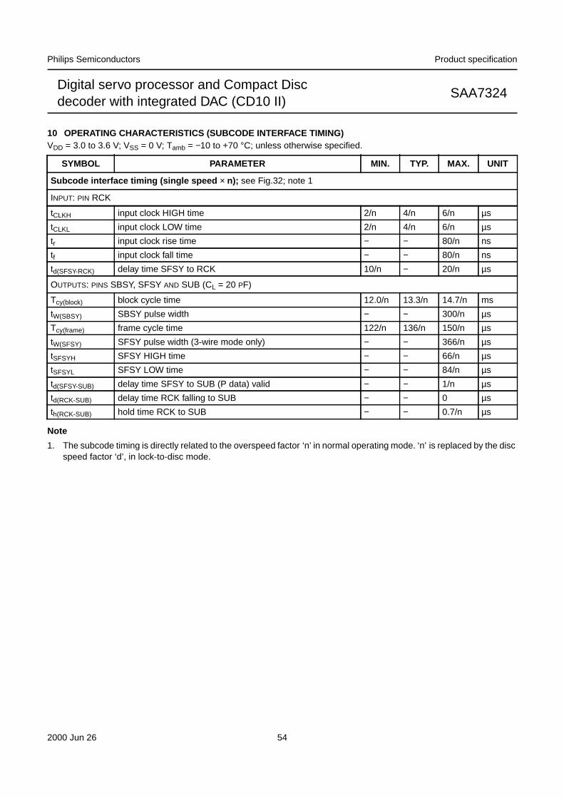
2000 Jun 26 54
Philips Semiconductors Product specification
Digital servo processor and Compact Discdecoder with integrated DAC (CD10 II)
SAA7324
10 OPERATING CHARACTERISTICS (SUBCODE INTERFACE TIMING)VDD = 3.0 to 3.6 V; VSS = 0 V; Tamb = −10 to +70 °C; unless otherwise specified.
Note
1. The subcode timing is directly related to the overspeed factor ‘n’ in normal operating mode. ‘n’ is replaced by the discspeed factor ‘d’, in lock-to-disc mode.
SYMBOL PARAMETER MIN. TYP. MAX. UNIT
Subcode interface timing (single speed × n); see Fig.32; note 1
INPUT: PIN RCK
tCLKH input clock HIGH time 2/n 4/n 6/n µs
tCLKL input clock LOW time 2/n 4/n 6/n µs
tr input clock rise time − − 80/n ns
tf input clock fall time − − 80/n ns
td(SFSY-RCK) delay time SFSY to RCK 10/n − 20/n µs
OUTPUTS: PINS SBSY, SFSY AND SUB (CL = 20 PF)
Tcy(block) block cycle time 12.0/n 13.3/n 14.7/n ms
tW(SBSY) SBSY pulse width − − 300/n µs
Tcy(frame) frame cycle time 122/n 136/n 150/n µs
tW(SFSY) SFSY pulse width (3-wire mode only) − − 366/n µs
tSFSYH SFSY HIGH time − − 66/n µs
tSFSYL SFSY LOW time − − 84/n µs
td(SFSY-SUB) delay time SFSY to SUB (P data) valid − − 1/n µs
td(RCK-SUB) delay time RCK falling to SUB − − 0 µs
th(RCK-SUB) hold time RCK to SUB − − 0.7/n µs
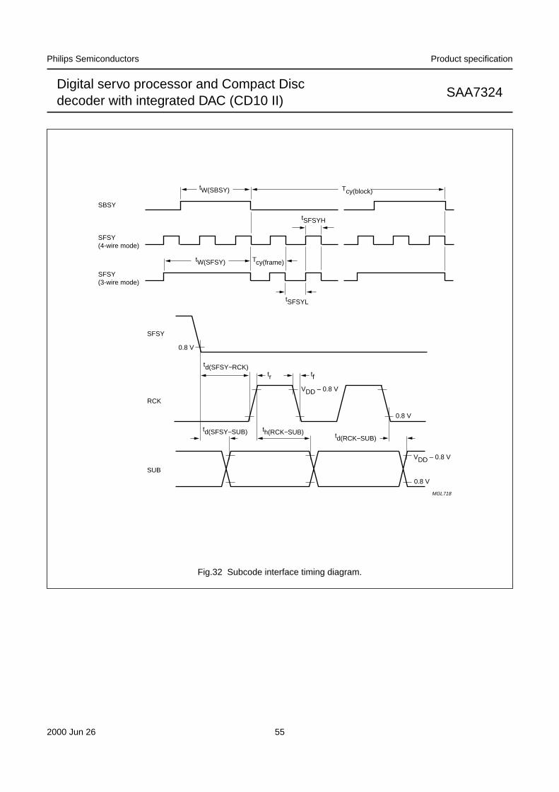
2000 Jun 26 55
Philips Semiconductors Product specification
Digital servo processor and Compact Discdecoder with integrated DAC (CD10 II)
SAA7324
handbook, full pagewidth tW(SBSY)
tW(SFSY)
tr
VDD – 0.8 V
VDD – 0.8 V
tSFSYL
tSFSYH
Tcy(block)
Tcy(frame)
tf
td(SFSY−RCK)
td(SFSY−SUB) th(RCK−SUB) td(RCK−SUB)
SBSY
SFSY
RCK
SUB
SFSY(4-wire mode)
SFSY(3-wire mode)
0.8 V
0.8 V
0.8 V
MGL718
Fig.32 Subcode interface timing diagram.
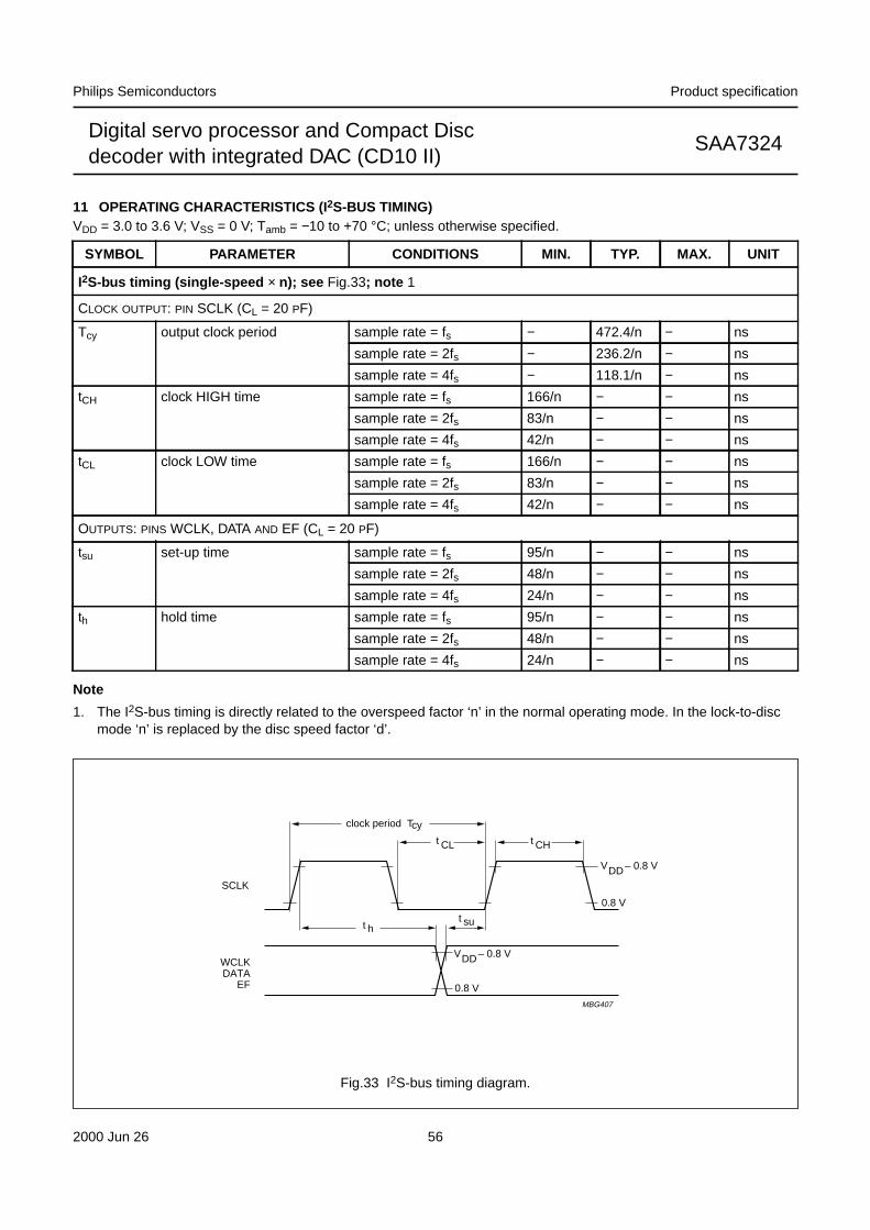
2000 Jun 26 56
Philips Semiconductors Product specification
Digital servo processor and Compact Discdecoder with integrated DAC (CD10 II)
SAA7324
11 OPERATING CHARACTERISTICS (I 2S-BUS TIMING)VDD = 3.0 to 3.6 V; VSS = 0 V; Tamb = −10 to +70 °C; unless otherwise specified.
Note
1. The I2S-bus timing is directly related to the overspeed factor ‘n’ in the normal operating mode. In the lock-to-discmode ‘n’ is replaced by the disc speed factor ‘d’.
SYMBOL PARAMETER CONDITIONS MIN. TYP. MAX. UNIT
I2S-bus timing (single-speed × n); see Fig.33; note 1
CLOCK OUTPUT: PIN SCLK (CL = 20 PF)
Tcy output clock period sample rate = fs − 472.4/n − ns
sample rate = 2fs − 236.2/n − ns
sample rate = 4fs − 118.1/n − ns
tCH clock HIGH time sample rate = fs 166/n − − ns
sample rate = 2fs 83/n − − ns
sample rate = 4fs 42/n − − ns
tCL clock LOW time sample rate = fs 166/n − − ns
sample rate = 2fs 83/n − − ns
sample rate = 4fs 42/n − − ns
OUTPUTS: PINS WCLK, DATA AND EF (CL = 20 PF)
tsu set-up time sample rate = fs 95/n − − ns
sample rate = 2fs 48/n − − ns
sample rate = 4fs 24/n − − ns
th hold time sample rate = fs 95/n − − ns
sample rate = 2fs 48/n − − ns
sample rate = 4fs 24/n − − ns
DDV – 0.8 V
0.8 V
DDV – 0.8 V
0.8 V
t CH
MBG407
t CL
clock period Tcy
SCLK
WCLKDATA
EF
t ht su
Fig.33 I2S-bus timing diagram.
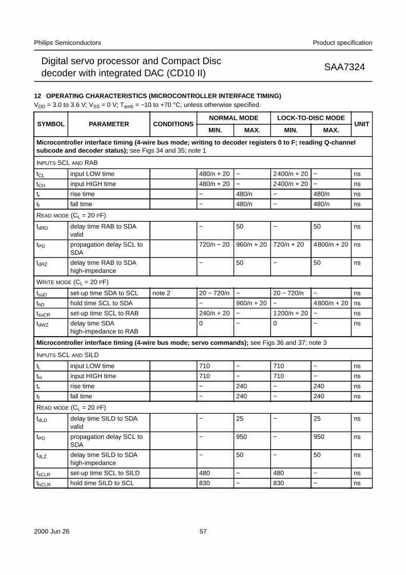
2000 Jun 26 57
Philips Semiconductors Product specification
Digital servo processor and Compact Discdecoder with integrated DAC (CD10 II)
SAA7324
12 OPERATING CHARACTERISTICS (MICROCONTROLLER INTERFACE TIMING)VDD = 3.0 to 3.6 V; VSS = 0 V; Tamb = −10 to +70 °C; unless otherwise specified.
SYMBOL PARAMETER CONDITIONSNORMAL MODE LOCK-TO-DISC MODE
UNITMIN. MAX. MIN. MAX.
Microcontroller interface timing (4-wire bus mode; writing to decoder registers 0 to F; reading Q-channelsubcode and decoder status); see Figs 34 and 35; note 1
INPUTS SCL AND RAB
tCL input LOW time 480/n + 20 − 2400/n + 20 − ns
tCH input HIGH time 480/n + 20 − 2400/n + 20 − ns
tr rise time − 480/n − 480/n ns
tf fall time − 480/n − 480/n ns
READ MODE (CL = 20 PF)
tdRD delay time RAB to SDAvalid
− 50 − 50 ns
tPD propagation delay SCL toSDA
720/n − 20 960/n + 20 720/n + 20 4800/n + 20 ns
tdRZ delay time RAB to SDAhigh-impedance
− 50 − 50 ns
WRITE MODE (CL = 20 PF)
tsuD set-up time SDA to SCL note 2 20 − 720/n − 20 − 720/n − ns
thD hold time SCL to SDA − 960/n + 20 − 4800/n + 20 ns
tsuCR set-up time SCL to RAB 240/n + 20 − 1200/n + 20 − ns
tdWZ delay time SDAhigh-impedance to RAB
0 − 0 − ns
Microcontroller interface timing (4-wire bus mode; servo commands); see Figs 36 and 37; note 3
INPUTS SCL AND SILD
tL input LOW time 710 − 710 − ns
tH input HIGH time 710 − 710 − ns
tr rise time − 240 − 240 ns
tf fall time − 240 − 240 ns
READ MODE (CL = 20 PF)
tdLD delay time SILD to SDAvalid
− 25 − 25 ns
tPD propagation delay SCL toSDA
− 950 − 950 ns
tdLZ delay time SILD to SDAhigh-impedance
− 50 − 50 ns
tsCLR set-up time SCL to SILD 480 − 480 − ns
thCLR hold time SILD to SCL 830 − 830 − ns
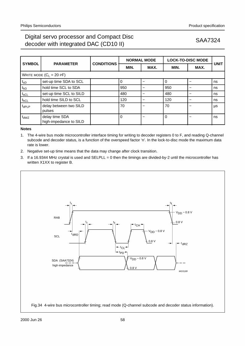
2000 Jun 26 58
Philips Semiconductors Product specification
Digital servo processor and Compact Discdecoder with integrated DAC (CD10 II)
SAA7324
Notes
1. The 4-wire bus mode microcontroller interface timing for writing to decoder registers 0 to F, and reading Q-channelsubcode and decoder status, is a function of the overspeed factor ‘n’. In the lock-to-disc mode the maximum datarate is lower.
2. Negative set-up time means that the data may change after clock transition.
3. If a 16.9344 MHz crystal is used and SELPLL = 0 then the timings are divided-by-2 until the microcontroller haswritten X1XX to register B.
WRITE MODE (CL = 20 PF)
tsD set-up time SDA to SCL 0 − 0 − ns
thD hold time SCL to SDA 950 − 950 − ns
tsCL set-up time SCL to SILD 480 − 480 − ns
thCL hold time SILD to SCL 120 − 120 − ns
tdPLP delay between two SILDpulses
70 − 70 − µs
tdWZ delay time SDAhigh-impedance to SILD
0 − 0 − ns
SYMBOL PARAMETER CONDITIONSNORMAL MODE LOCK-TO-DISC MODE
UNITMIN. MAX. MIN. MAX.
SDA (SAA7324)
SCL
RABtr
tr
0.8 V
tf
tf
VDD − 0.8 V
VDD − 0.8 V
0.8 V
VDD − 0.8 V
0.8 V
tPD
tCL
tCH
tdRD
tdRZ
high-impedance
MGS189
Fig.34 4-wire bus microcontroller timing; read mode (Q-channel subcode and decoder status information).
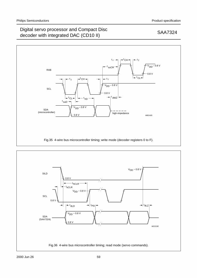
2000 Jun 26 59
Philips Semiconductors Product specification
Digital servo processor and Compact Discdecoder with integrated DAC (CD10 II)
SAA7324
handbook, full pagewidth
SCL
RAB
t rt f
DDV – 0.8 V
0.8 V
DDV – 0.8 V
0.8 V
t hDtCL
t CH
t dWZ
MBG405
t r t f
DDV – 0.8 V
0.8 Vt CL
tCH
t suCR
t suD
SDA (microcontroller) high-impedance
Fig.35 4-wire bus microcontroller timing; write mode (decoder registers 0 to F).
handbook, full pagewidth
tdLD
thCLRtsCLR
tPD tdLZ
0.8 V
0.8 V
0.8 V
VDD − 0.8 V
VDD − 0.8 V
VDD − 0.8 V
SILD
SCL
SDA(SAA7324)
MGS190
Fig.36 4-wire bus microcontroller timing; read mode (servo commands).
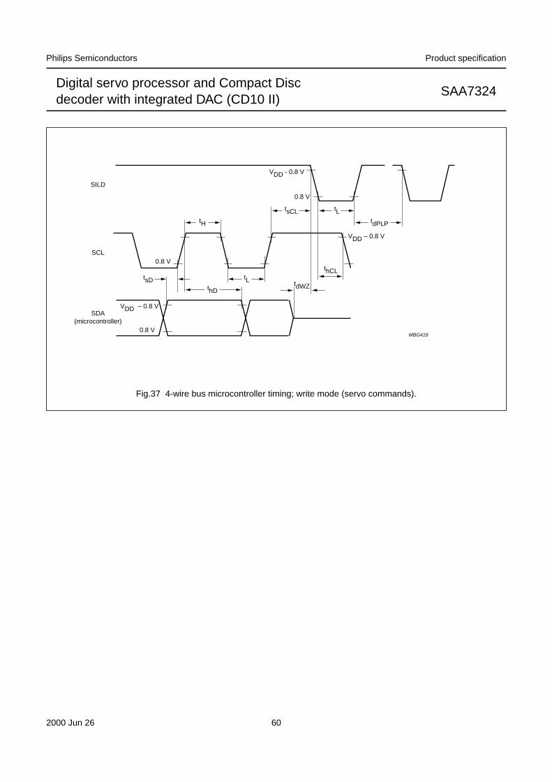
2000 Jun 26 60
Philips Semiconductors Product specification
Digital servo processor and Compact Discdecoder with integrated DAC (CD10 II)
SAA7324
handbook, full pagewidth
tdPLP
tLtsCL
tdWZ
thCL
tH
thD
tsD tL
0.8 V
0.8 V
0.8 V
VDD - 0.8 V
VDD – 0.8 V
VDD – 0.8 V
SILD
SCL
SDA(microcontroller)
MBG416
Fig.37 4-wire bus microcontroller timing; write mode (servo commands).
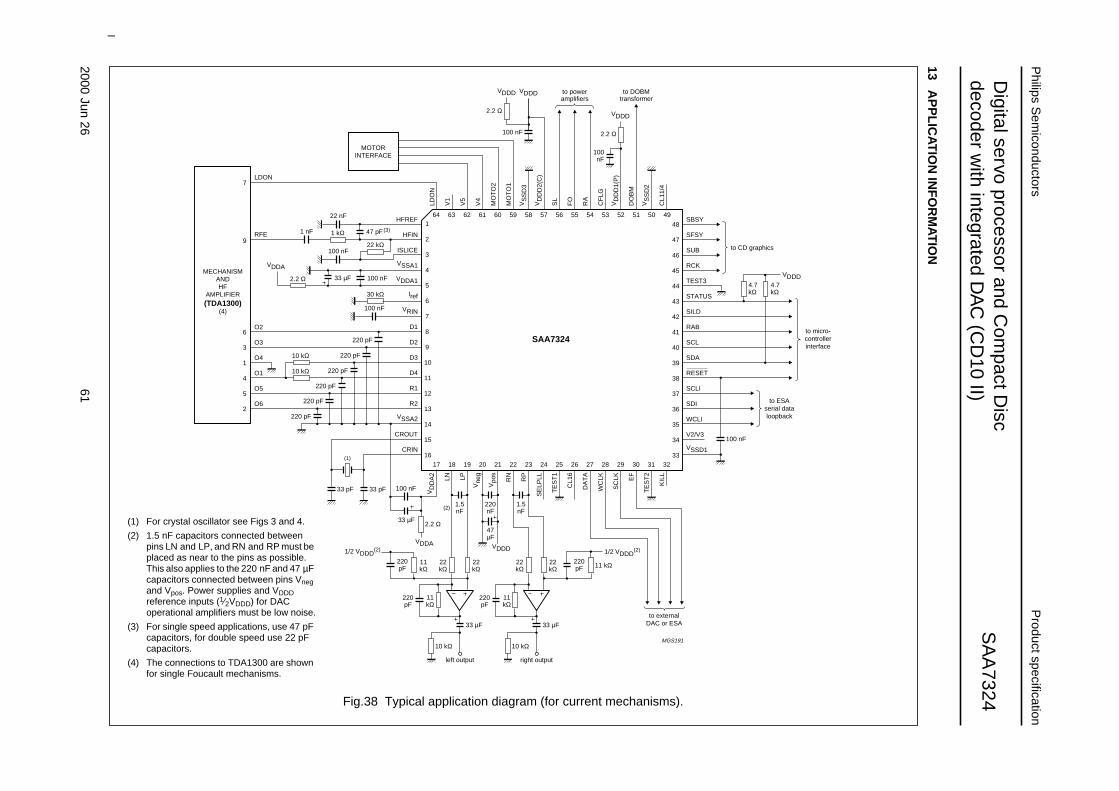
2000Jun
2661
Philips S
emiconductors
Product specification
Digital servo processor and C
ompact D
iscdecoder w
ith integrated DA
C (C
D10 II)
SA
A7324
This text is here in white to force landscape pages to be rotated correctly when browsing through the pdf in the Acrobat reader.This text is here in_white to force landscape pages to be rotated correctly when browsing through the pdf in the Acrobat reader.This text is here inThis text is here inwhite to force landscape pages to be rotated correctly when browsing through the pdf in the Acrobat reader. white to force landscape pages to be ...
13A
PP
LICAT
ION
INF
OR
MAT
ION
book, full pagewidth
MGS191
22 kΩ
1 kΩ
10 kΩ
10 kΩ
30 kΩ
2.2 Ω
SAA7324
MECHANISMANDHF
AMPLIFIER(TDA1300)
(4)
1
2
3
4
5
6
7
8
9
10
11
12
13
14
15
16
48
47
46
45
44
43
42
41
40
39
38
37
36
35
34
SBSY
SFSY
SUB
RCK
TEST3
STATUS
SILD
RAB
SCL
SDA
SCLI
SDI
WCLI
V2/V3
VSSD1
HFREF
HFIN
ISLICE
VSSA1
VDDA1
VDDA
Iref
VRIN
D1
D2
D3
D4
R1
R2
VSSA2
CROUT
CRIN33
17 18 19 20
left output
21 22 23 24 25 26 27 28 29
to externalDAC or ESA
30 31 32
64 63 62 61 60 59 58 57 56 55
to poweramplifiers
54 53 52 51
to DOBMtransformer
to CD graphics
50
LDO
N
V1
V5
V4
MO
TO
2
MO
TO
1
VS
SD
3
VD
DD
2(C
)
SL
FO
RA
CF
LG
VD
DD
1(P
)
DO
BM
VS
SD
2
CL1
1/4
VD
DA
2
LN LP
Vne
g
Vpo
s
RN
RP
SE
LPLL
TE
ST
1
CL1
6
DA
TA
WC
LK
SC
LK EF
TE
ST
2
KIL
L
49
RESET
33 µF
33 pF 33 pF
100 nF
100 nF
220 pF
220 pF
220 pF
220 pF
220 pF
220 pF
O6
O5
O1
O4
O3
O2
2
5
4
1
3
6
9
7
RFE
LDON
47 pF(3)
(1)
100 nF
1.5nF
220nF
1.5nF
(2)
100 nF
1 nF
22 nF
100 nF
VDDA VDDD 1/2 VDDD(2)1/2 VDDD
(2)
MOTORINTERFACE
to micro-controllerinterface
to ESAserial dataloopback
VDDD
VDDD
2.2 Ω
VDDD
2.2 Ω
4.7kΩ
VDDD4.7kΩ
100nF
100 nF
47µF
33 µF 33 µF
33 µF2.2 Ω
22kΩ
11kΩ
22kΩ
220pF
11kΩ
10 kΩ
right output
22kΩ
22kΩ 11 kΩ
220pF
220pF
220pF
11kΩ
10 kΩ
Fig.38 Typical application diagram (for current mechanisms).
(1) For crystal oscillator see Figs 3 and 4.
(2) 1.5 nF capacitors connected betweenpins LN and LP, and RN and RP must beplaced as near to the pins as possible.This also applies to the 220 nF and 47 µFcapacitors connected between pins Vnegand Vpos. Power supplies and VDDDreference inputs (1⁄2VDDD) for DACoperational amplifiers must be low noise.
(3) For single speed applications, use 47 pFcapacitors, for double speed use 22 pFcapacitors.
(4) The connections to TDA1300 are shownfor single Foucault mechanisms.
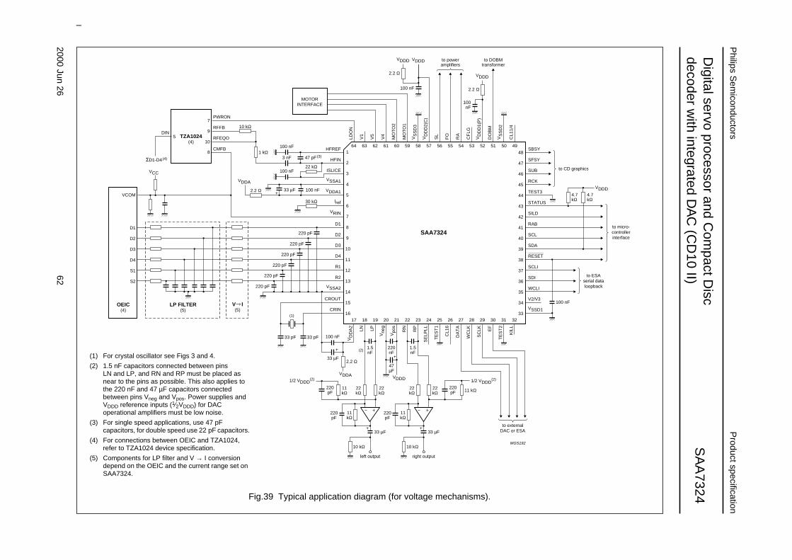
2000Jun
2662
Philips S
emiconductors
Product specification
Digital servo processor and C
ompact D
iscdecoder w
ith integrated DA
C (C
D10 II)
SA
A7324
This text is here in white to force landscape pages to be rotated correctly when browsing through the pdf in the Acrobat reader.This text is here in_white to force landscape pages to be rotated correctly when browsing through the pdf in the Acrobat reader.This text is here inThis text is here inwhite to force landscape pages to be rotated correctly when browsing through the pdf in the Acrobat reader. white to force landscape pages to be ...
ook, full pagewidth
MGS192
22 kΩ
10 kΩ
1 kΩ
30 kΩ
2.2 Ω
SAA7324
LP FILTER(5)
V I(5)
OEIC(4)
TZA1024(4)
1
RFEQO
2
3
4
5
6
7
8
9
10
11
12
13
14
15
16
48
47
46
45
44
43
42
41
40
39
38
37
36
35
34
SBSY
SFSY
SUB
RCK
TEST3
STATUS
SILD
RAB
SCL
SDA
SCLI
SDI
WCLI
V2/V3
VSSD1
HFREF
HFIN
ISLICE
VSSA1
VDDA1
VDDA
Iref
VRIN
D1
D2
D3
D4
R1
R2
VSSA2
CROUT
CRIN33
17 18 19 20
left output
21 22 23 24 25 26 27 28 29
to externalDAC or ESA
30 31 32
64 63 62 61 60 59 58 57 56 55
to poweramplifiers
54 53 52 51
to DOBMtransformer
to CD graphics
50
LDO
N
V1
V5
V4
MO
TO
2
MO
TO
1
VS
SD
3
VD
DD
2(C
)
SL
FO
RA
CF
LG
VD
DD
1(P
)
DO
BM
VS
SD
2
CL1
1/4
VD
DA
2
LN LP
Vne
g
Vpo
s
RN
RP
SE
LPLL
TE
ST
1
CL1
6
DA
TA
WC
LK
SC
LK EF
TE
ST
2
KIL
L
49
RESET
33 µF
33 pF 33 pF
100 nF
100 nF
220 pF
220 pF
220 pF
220 pF
220 pF
220 pFS2
S1
D4
D3
D2
D1
VCOM
10
CMFB8
DIN
ΣD1-D4(4)
RFFB9
PWRON7
5
47 pF(3)
(1)
100 nF
1.5nF
220nF
1.5nF
(2)
100 nF
3 nF
100 nF
VDDA VDDD 1/2 VDDD(2)1/2 VDDD
(2)
MOTORINTERFACE
to micro-controllerinterface
to ESAserial dataloopback
VCC
VDDD
VDDD
2.2 Ω
VDDD
2.2 Ω
4.7kΩ
VDDD4.7kΩ
100nF
100 nF
47µF
33 µF 33 µF
33 µF2.2 Ω
22kΩ
11kΩ
22kΩ
220pF
11kΩ
10 kΩ
right output
22kΩ
22kΩ 11 kΩ
220pF
220pF
220pF
11kΩ
10 kΩ
Fig.39 Typical application diagram (for voltage mechanisms).
(1) For crystal oscillator see Figs 3 and 4.
(2) 1.5 nF capacitors connected between pinsLN and LP, and RN and RP must be placed asnear to the pins as possible. This also applies tothe 220 nF and 47 µF capacitors connectedbetween pins Vneg and Vpos. Power supplies andVDDD reference inputs (1⁄2VDDD) for DACoperational amplifiers must be low noise.
(3) For single speed applications, use 47 pFcapacitors, for double speed use 22 pF capacitors.
(4) For connections between OEIC and TZA1024,refer to TZA1024 device specification.
(5) Components for LP filter and V → I conversiondepend on the OEIC and the current range set onSAA7324.
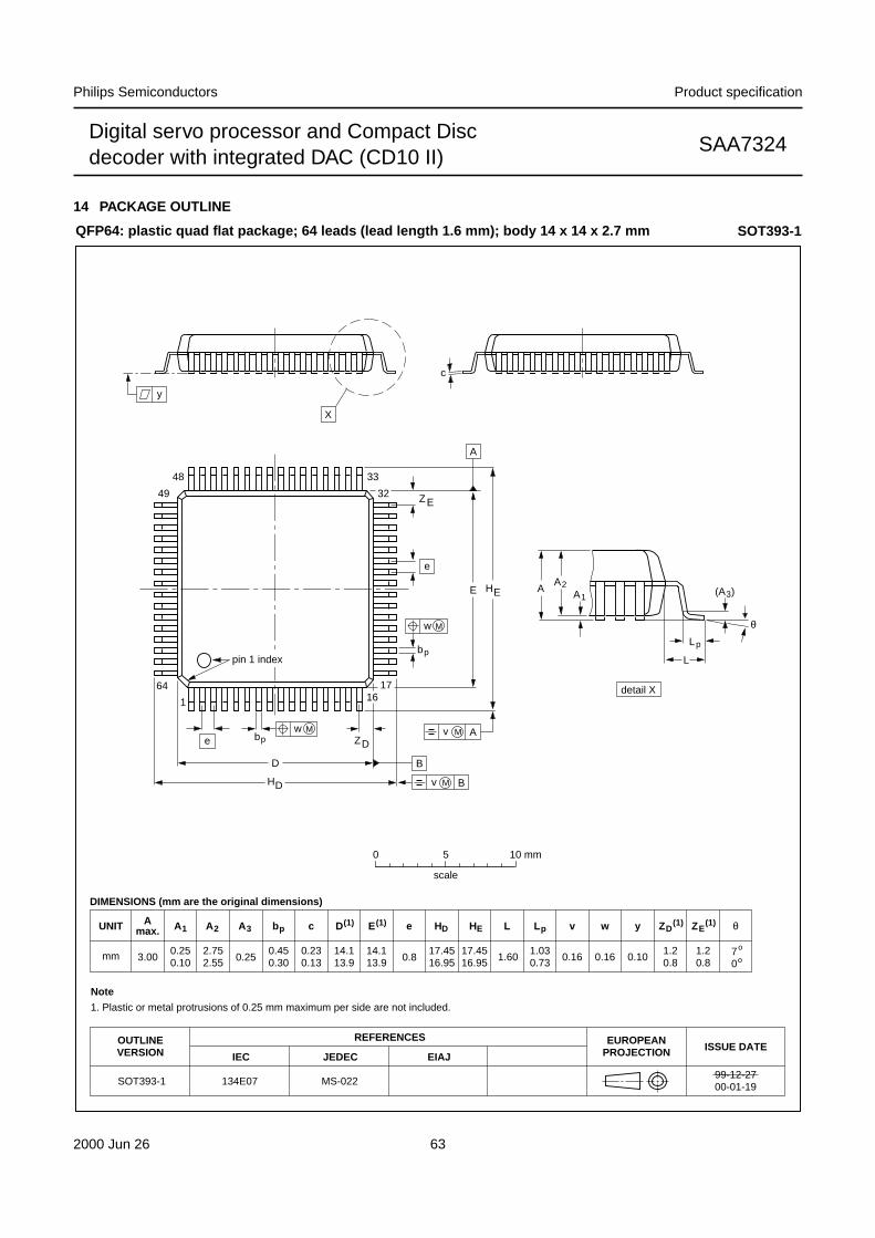
2000 Jun 26 63
Philips Semiconductors Product specification
Digital servo processor and Compact Discdecoder with integrated DAC (CD10 II)
SAA7324
14 PACKAGE OUTLINE
UNIT A1 A2 A3 bp c E(1) e HE L Lp Zywv θ
REFERENCESOUTLINEVERSION
EUROPEANPROJECTION ISSUE DATE
IEC JEDEC EIAJ
mm 0.250.10
2.752.55 0.25
0.450.30
0.230.13
14.113.9 0.8
17.4516.95
1.20.8
70
o
o0.16 0.100.161.60
DIMENSIONS (mm are the original dimensions)
Note
1. Plastic or metal protrusions of 0.25 mm maximum per side are not included.
1.030.73
SOT393-1 134E07 MS-02299-12-2700-01-19
D(1) (1)(1)
14.113.9
HD
17.4516.95
EZ
1.20.8
D
e
θ
E A1A
Lp
detail X
L
(A )3
B
16
y
c
EHA2
D
ZD
A
ZE
e
v M A
1
64
49
48 33
32
17
X
bp
DH
bp
v M B
w M
w M
0 5 10 mm
scale
pin 1 index
QFP64: plastic quad flat package; 64 leads (lead length 1.6 mm); body 14 x 14 x 2.7 mm SOT393-1
Amax.
3.00
2000 Jun 26 64
Philips Semiconductors Product specification
Digital servo processor and Compact Discdecoder with integrated DAC (CD10 II)
SAA7324
15 SOLDERING
15.1 Introduction to soldering surface mountpackages
This text gives a very brief insight to a complex technology.A more in-depth account of soldering ICs can be found inour “Data Handbook IC26; Integrated Circuit Packages”(document order number 9398 652 90011).
There is no soldering method that is ideal for all surfacemount IC packages. Wave soldering is not always suitablefor surface mount ICs, or for printed-circuit boards withhigh population densities. In these situations reflowsoldering is often used.
15.2 Reflow soldering
Reflow soldering requires solder paste (a suspension offine solder particles, flux and binding agent) to be appliedto the printed-circuit board by screen printing, stencilling orpressure-syringe dispensing before package placement.
Several methods exist for reflowing; for example,infrared/convection heating in a conveyor type oven.Throughput times (preheating, soldering and cooling) varybetween 100 and 200 seconds depending on heatingmethod.
Typical reflow peak temperatures range from215 to 250 °C. The top-surface temperature of thepackages should preferable be kept below 230 °C.
15.3 Wave soldering
Conventional single wave soldering is not recommendedfor surface mount devices (SMDs) or printed-circuit boardswith a high component density, as solder bridging andnon-wetting can present major problems.
To overcome these problems the double-wave solderingmethod was specifically developed.
If wave soldering is used the following conditions must beobserved for optimal results:
• Use a double-wave soldering method comprising aturbulent wave with high upward pressure followed by asmooth laminar wave.
• For packages with leads on two sides and a pitch (e):
– larger than or equal to 1.27 mm, the footprintlongitudinal axis is preferred to be parallel to thetransport direction of the printed-circuit board;
– smaller than 1.27 mm, the footprint longitudinal axismust be parallel to the transport direction of theprinted-circuit board.
The footprint must incorporate solder thieves at thedownstream end.
• For packages with leads on four sides, the footprint mustbe placed at a 45° angle to the transport direction of theprinted-circuit board. The footprint must incorporatesolder thieves downstream and at the side corners.
During placement and before soldering, the package mustbe fixed with a droplet of adhesive. The adhesive can beapplied by screen printing, pin transfer or syringedispensing. The package can be soldered after theadhesive is cured.
Typical dwell time is 4 seconds at 250 °C.A mildly-activated flux will eliminate the need for removalof corrosive residues in most applications.
15.4 Manual soldering
Fix the component by first soldering twodiagonally-opposite end leads. Use a low voltage (24 V orless) soldering iron applied to the flat part of the lead.Contact time must be limited to 10 seconds at up to300 °C.
When using a dedicated tool, all other leads can besoldered in one operation within 2 to 5 seconds between270 and 320 °C.
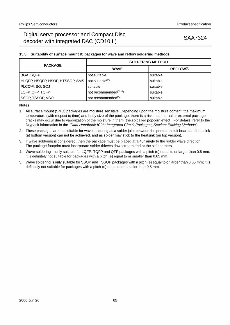
2000 Jun 26 65
Philips Semiconductors Product specification
Digital servo processor and Compact Discdecoder with integrated DAC (CD10 II)
SAA7324
15.5 Suitability of surface mount IC packages for wave and reflow soldering methods
Notes
1. All surface mount (SMD) packages are moisture sensitive. Depending upon the moisture content, the maximumtemperature (with respect to time) and body size of the package, there is a risk that internal or external packagecracks may occur due to vaporization of the moisture in them (the so called popcorn effect). For details, refer to theDrypack information in the “Data Handbook IC26; Integrated Circuit Packages; Section: Packing Methods”.
2. These packages are not suitable for wave soldering as a solder joint between the printed-circuit board and heatsink(at bottom version) can not be achieved, and as solder may stick to the heatsink (on top version).
3. If wave soldering is considered, then the package must be placed at a 45° angle to the solder wave direction.The package footprint must incorporate solder thieves downstream and at the side corners.
4. Wave soldering is only suitable for LQFP, TQFP and QFP packages with a pitch (e) equal to or larger than 0.8 mm;it is definitely not suitable for packages with a pitch (e) equal to or smaller than 0.65 mm.
5. Wave soldering is only suitable for SSOP and TSSOP packages with a pitch (e) equal to or larger than 0.65 mm; it isdefinitely not suitable for packages with a pitch (e) equal to or smaller than 0.5 mm.
PACKAGESOLDERING METHOD
WAVE REFLOW (1)
BGA, SQFP not suitable suitable
HLQFP, HSQFP, HSOP, HTSSOP, SMS not suitable(2) suitable
PLCC(3), SO, SOJ suitable suitable
LQFP, QFP, TQFP not recommended(3)(4) suitable
SSOP, TSSOP, VSO not recommended(5) suitable
2000 Jun 26 66
Philips Semiconductors Product specification
Digital servo processor and Compact Discdecoder with integrated DAC (CD10 II)
SAA7324
16 DATA SHEET STATUS
Note
1. Please consult the most recently issued data sheet before initiating or completing a design.
DATA SHEET STATUSPRODUCTSTATUS
DEFINITIONS (1)
Objective specification Development This data sheet contains the design target or goal specifications forproduct development. Specification may change in any manner withoutnotice.
Preliminary specification Qualification This data sheet contains preliminary data, and supplementary data will bepublished at a later date. Philips Semiconductors reserves the right tomake changes at any time without notice in order to improve design andsupply the best possible product.
Product specification Production This data sheet contains final specifications. Philips Semiconductorsreserves the right to make changes at any time without notice in order toimprove design and supply the best possible product.
17 DEFINITIONS
Short-form specification The data in a short-formspecification is extracted from a full data sheet with thesame type number and title. For detailed information seethe relevant data sheet or data handbook.
Limiting values definition Limiting values given are inaccordance with the Absolute Maximum Rating System(IEC 60134). Stress above one or more of the limitingvalues may cause permanent damage to the device.These are stress ratings only and operation of the deviceat these or at any other conditions above those given in theCharacteristics sections of the specification is not implied.Exposure to limiting values for extended periods mayaffect device reliability.
Application information Applications that aredescribed herein for any of these products are forillustrative purposes only. Philips Semiconductors makeno representation or warranty that such applications will besuitable for the specified use without further testing ormodification.
18 DISCLAIMERS
Life support applications These products are notdesigned for use in life support appliances, devices, orsystems where malfunction of these products canreasonably be expected to result in personal injury. PhilipsSemiconductors customers using or selling these productsfor use in such applications do so at their own risk andagree to fully indemnify Philips Semiconductors for anydamages resulting from such application.
Right to make changes Philips Semiconductorsreserves the right to make changes, without notice, in theproducts, including circuits, standard cells, and/orsoftware, described or contained herein in order toimprove design and/or performance. PhilipsSemiconductors assumes no responsibility or liability forthe use of any of these products, conveys no licence or titleunder any patent, copyright, or mask work right to theseproducts, and makes no representations or warranties thatthese products are free from patent, copyright, or maskwork right infringement, unless otherwise specified.
19 PURCHASE OF PHILIPS I2C COMPONENTS
Purchase of Philips I2C components conveys a license under the Philips’ I2C patent to use thecomponents in the I2C system provided the system conforms to the I2C specification defined byPhilips. This specification can be ordered using the code 9398 393 40011.
2000 Jun 26 67
Philips Semiconductors Product specification
Digital servo processor and Compact Discdecoder with integrated DAC (CD10 II)
SAA7324
NOTES

© Philips Electronics N.V. SCA
All rights are reserved. Reproduction in whole or in part is prohibited without the prior written consent of the copyright owner.
The information presented in this document does not form part of any quotation or contract, is believed to be accurate and reliable and may be changedwithout notice. No liability will be accepted by the publisher for any consequence of its use. Publication thereof does not convey nor imply any licenseunder patent- or other industrial or intellectual property rights.
Internet: http://www.semiconductors.philips.com
2000 70
Philips Semiconductors – a worldwide company
For all other countries apply to: Philips Semiconductors,Marketing Communications, Building BE-p, P.O. Box 218, 5600 MD EINDHOVEN,The Netherlands, Fax. +31 40 27 24825
Argentina: see South America
Australia: 3 Figtree Drive, HOMEBUSH, NSW 2140,Tel. +61 2 9704 8141, Fax. +61 2 9704 8139
Austria: Computerstr. 6, A-1101 WIEN, P.O. Box 213,Tel. +43 1 60 101 1248, Fax. +43 1 60 101 1210
Belarus: Hotel Minsk Business Center, Bld. 3, r. 1211, Volodarski Str. 6,220050 MINSK, Tel. +375 172 20 0733, Fax. +375 172 20 0773
Belgium: see The Netherlands
Brazil: see South America
Bulgaria: Philips Bulgaria Ltd., Energoproject, 15th floor,51 James Bourchier Blvd., 1407 SOFIA,Tel. +359 2 68 9211, Fax. +359 2 68 9102
Canada: PHILIPS SEMICONDUCTORS/COMPONENTS,Tel. +1 800 234 7381, Fax. +1 800 943 0087
China/Hong Kong: 501 Hong Kong Industrial Technology Centre,72 Tat Chee Avenue, Kowloon Tong, HONG KONG,Tel. +852 2319 7888, Fax. +852 2319 7700
Colombia: see South America
Czech Republic: see Austria
Denmark: Sydhavnsgade 23, 1780 COPENHAGEN V,Tel. +45 33 29 3333, Fax. +45 33 29 3905
Finland: Sinikalliontie 3, FIN-02630 ESPOO,Tel. +358 9 615 800, Fax. +358 9 6158 0920
France: 51 Rue Carnot, BP317, 92156 SURESNES Cedex,Tel. +33 1 4099 6161, Fax. +33 1 4099 6427
Germany: Hammerbrookstraße 69, D-20097 HAMBURG,Tel. +49 40 2353 60, Fax. +49 40 2353 6300
Hungary: see Austria
India: Philips INDIA Ltd, Band Box Building, 2nd floor,254-D, Dr. Annie Besant Road, Worli, MUMBAI 400 025,Tel. +91 22 493 8541, Fax. +91 22 493 0966
Indonesia: PT Philips Development Corporation, Semiconductors Division,Gedung Philips, Jl. Buncit Raya Kav.99-100, JAKARTA 12510,Tel. +62 21 794 0040 ext. 2501, Fax. +62 21 794 0080
Ireland: Newstead, Clonskeagh, DUBLIN 14,Tel. +353 1 7640 000, Fax. +353 1 7640 200
Israel: RAPAC Electronics, 7 Kehilat Saloniki St, PO Box 18053,TEL AVIV 61180, Tel. +972 3 645 0444, Fax. +972 3 649 1007
Italy: PHILIPS SEMICONDUCTORS, Via Casati, 23 - 20052 MONZA (MI),Tel. +39 039 203 6838, Fax +39 039 203 6800
Japan: Philips Bldg 13-37, Kohnan 2-chome, Minato-ku,TOKYO 108-8507, Tel. +81 3 3740 5130, Fax. +81 3 3740 5057
Korea: Philips House, 260-199 Itaewon-dong, Yongsan-ku, SEOUL,Tel. +82 2 709 1412, Fax. +82 2 709 1415
Malaysia: No. 76 Jalan Universiti, 46200 PETALING JAYA, SELANGOR,Tel. +60 3 750 5214, Fax. +60 3 757 4880
Mexico: 5900 Gateway East, Suite 200, EL PASO, TEXAS 79905,Tel. +9-5 800 234 7381, Fax +9-5 800 943 0087
Middle East: see Italy
Netherlands: Postbus 90050, 5600 PB EINDHOVEN, Bldg. VB,Tel. +31 40 27 82785, Fax. +31 40 27 88399
New Zealand: 2 Wagener Place, C.P.O. Box 1041, AUCKLAND,Tel. +64 9 849 4160, Fax. +64 9 849 7811
Norway: Box 1, Manglerud 0612, OSLO,Tel. +47 22 74 8000, Fax. +47 22 74 8341
Pakistan: see Singapore
Philippines: Philips Semiconductors Philippines Inc.,106 Valero St. Salcedo Village, P.O. Box 2108 MCC, MAKATI,Metro MANILA, Tel. +63 2 816 6380, Fax. +63 2 817 3474
Poland : Al.Jerozolimskie 195 B, 02-222 WARSAW,Tel. +48 22 5710 000, Fax. +48 22 5710 001
Portugal: see Spain
Romania: see Italy
Russia: Philips Russia, Ul. Usatcheva 35A, 119048 MOSCOW,Tel. +7 095 755 6918, Fax. +7 095 755 6919
Singapore: Lorong 1, Toa Payoh, SINGAPORE 319762,Tel. +65 350 2538, Fax. +65 251 6500
Slovakia: see Austria
Slovenia: see Italy
South Africa: S.A. PHILIPS Pty Ltd., 195-215 Main Road Martindale,2092 JOHANNESBURG, P.O. Box 58088 Newville 2114,Tel. +27 11 471 5401, Fax. +27 11 471 5398
South America: Al. Vicente Pinzon, 173, 6th floor,04547-130 SÃO PAULO, SP, Brazil,Tel. +55 11 821 2333, Fax. +55 11 821 2382
Spain: Balmes 22, 08007 BARCELONA,Tel. +34 93 301 6312, Fax. +34 93 301 4107
Sweden: Kottbygatan 7, Akalla, S-16485 STOCKHOLM,Tel. +46 8 5985 2000, Fax. +46 8 5985 2745
Switzerland: Allmendstrasse 140, CH-8027 ZÜRICH,Tel. +41 1 488 2741 Fax. +41 1 488 3263
Taiwan: Philips Semiconductors, 5F, No. 96, Chien Kuo N. Rd., Sec. 1,TAIPEI, Taiwan Tel. +886 2 2134 2451, Fax. +886 2 2134 2874
Thailand: PHILIPS ELECTRONICS (THAILAND) Ltd.,60/14 MOO 11, Bangna Trad Road KM. 3, Bagna, BANGKOK 10260,Tel. +66 2 361 7910, Fax. +66 2 398 3447
Turkey: Yukari Dudullu, Org. San. Blg., 2.Cad. Nr. 28 81260 Umraniye,ISTANBUL, Tel. +90 216 522 1500, Fax. +90 216 522 1813
Ukraine : PHILIPS UKRAINE, 4 Patrice Lumumba str., Building B, Floor 7,252042 KIEV, Tel. +380 44 264 2776, Fax. +380 44 268 0461
United Kingdom: Philips Semiconductors Ltd., 276 Bath Road, Hayes,MIDDLESEX UB3 5BX, Tel. +44 208 730 5000, Fax. +44 208 754 8421
United States: 811 East Arques Avenue, SUNNYVALE, CA 94088-3409,Tel. +1 800 234 7381, Fax. +1 800 943 0087
Uruguay: see South America
Vietnam: see Singapore
Yugoslavia: PHILIPS, Trg N. Pasica 5/v, 11000 BEOGRAD,Tel. +381 11 3341 299, Fax.+381 11 3342 553
Printed in The Netherlands 753503/02/pp68 Date of release: 2000 Jun 26 Document order number: 9397 750 06991