Embed Size (px)
Citation preview
Page 1 of 44
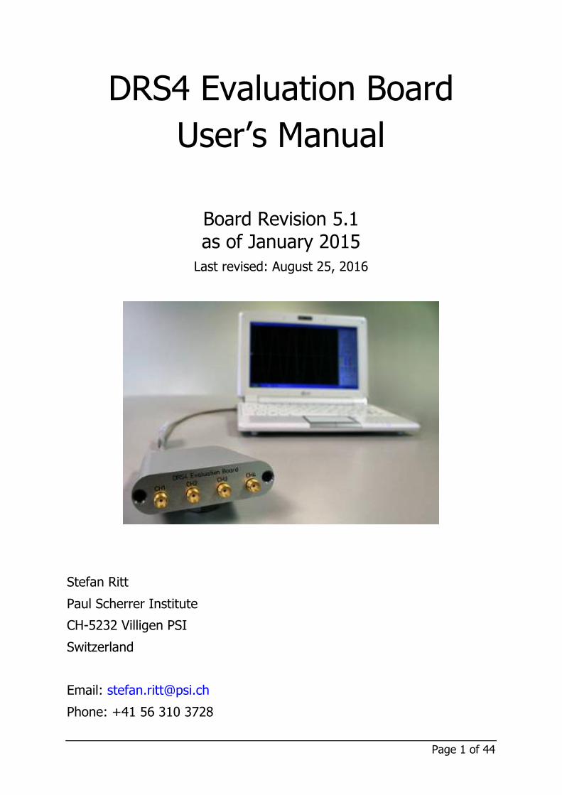
DRS4 Evaluation Board User’s Manual
Board Revision 5.1 as of January 2015
Last revised: August 25, 2016
Stefan Ritt
Paul Scherrer Institute
CH-5232 Villigen PSI
Switzerland
Email: [email protected]
Phone: +41 56 310 3728
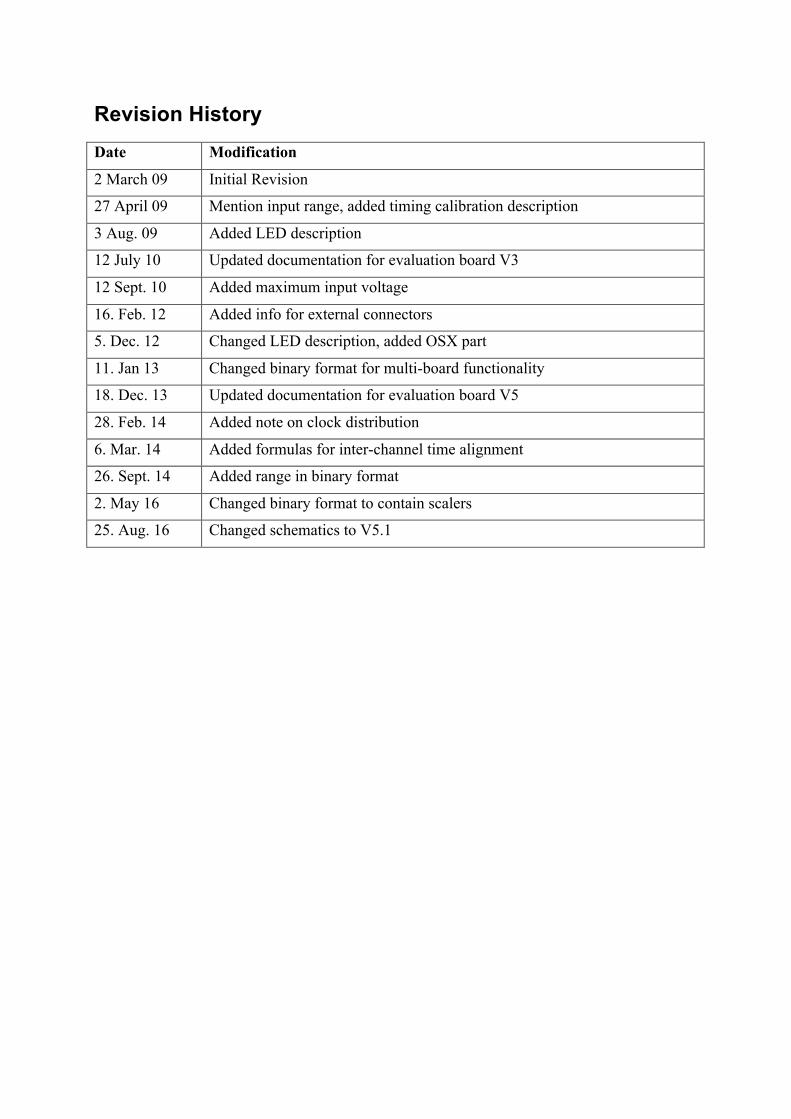
Revision History Date Modification
2 March 09 Initial Revision
27 April 09 Mention input range, added timing calibration description
3 Aug. 09 Added LED description
12 July 10 Updated documentation for evaluation board V3
12 Sept. 10 Added maximum input voltage
16. Feb. 12 Added info for external connectors
5. Dec. 12 Changed LED description, added OSX part
11. Jan 13 Changed binary format for multi-board functionality
18. Dec. 13 Updated documentation for evaluation board V5
28. Feb. 14 Added note on clock distribution
6. Mar. 14 Added formulas for inter-channel time alignment
26. Sept. 14 Added range in binary format
2. May 16 Changed binary format to contain scalers
25. Aug. 16 Changed schematics to V5.1
Page 3 of 44
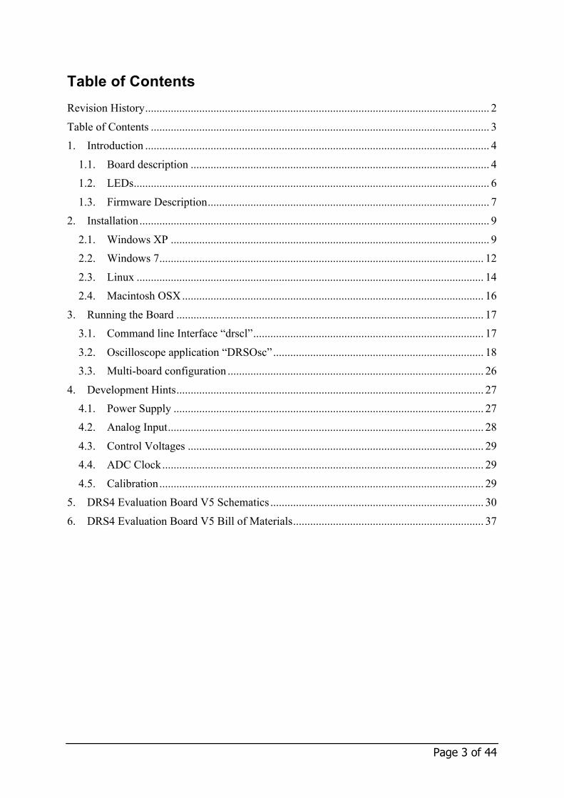
Table of Contents Revision History ......................................................................................................................... 2Table of Contents ....................................................................................................................... 31. Introduction ......................................................................................................................... 4
1.1. Board description ......................................................................................................... 41.2. LEDs ............................................................................................................................. 61.3. Firmware Description ................................................................................................... 7
2. Installation ........................................................................................................................... 92.1. Windows XP ................................................................................................................ 92.2. Windows 7 .................................................................................................................. 122.3. Linux .......................................................................................................................... 142.4. Macintosh OSX .......................................................................................................... 16
3. Running the Board ............................................................................................................ 173.1. Command line Interface “drscl” ................................................................................. 173.2. Oscilloscope application “DRSOsc” .......................................................................... 183.3. Multi-board configuration .......................................................................................... 26
4. Development Hints ............................................................................................................ 274.1. Power Supply ............................................................................................................. 274.2. Analog Input ............................................................................................................... 284.3. Control Voltages ........................................................................................................ 294.4. ADC Clock ................................................................................................................. 294.5. Calibration .................................................................................................................. 29
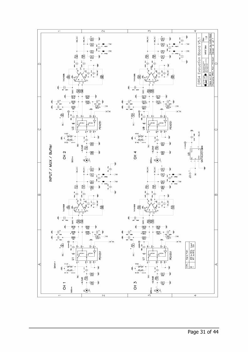
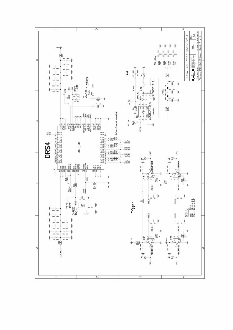
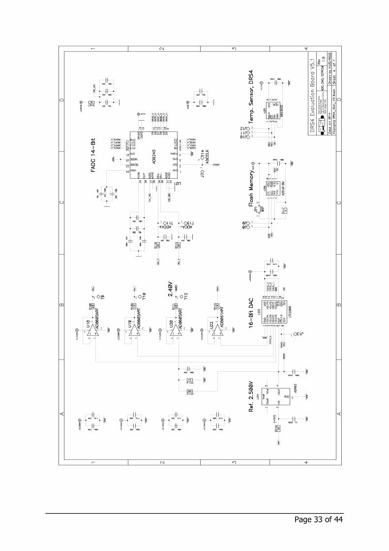
5. DRS4 Evaluation Board V5 Schematics ........................................................................... 306. DRS4 Evaluation Board V5 Bill of Materials ................................................................... 37
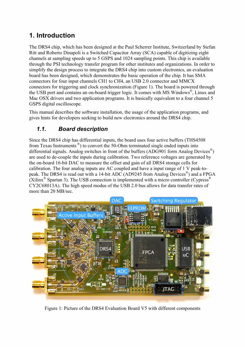
1. Introduction The DRS4 chip, which has been designed at the Paul Scherrer Institute, Switzerland by Stefan Ritt and Roberto Dinapoli is a Switched Capacitor Array (SCA) capable of digitizing eight channels at sampling speeds up to 5 GSPS and 1024 sampling points. This chip is available through the PSI technology transfer program for other institutes and organizations. In order to simplify the design process to integrate the DRS4 chip into custom electronics, an evaluation board has been designed, which demonstrates the basic operation of the chip. It has SMA connectors for four input channels CH1 to CH4, an USB 2.0 connector and MMCX connectors for triggering and clock synchronization (Figure 1). The board is powered through the USB port and contains an on-board trigger logic. It comes with MS Windows®, Linux and Mac OSX drivers and two application programs. It is basically equivalent to a four channel 5 GSPS digital oscilloscope.
This manual describes the software installation, the usage of the application programs, and gives hints for developers seeking to build new electronics around the DRS4 chip.
1.1. Board description
Since the DRS4 chip has differential inputs, the board uses four active buffers (THS4508 from Texas Instruments ®) to convert the 50-Ohm terminated single ended inputs into differential signals. Analog switches in front of the buffers (ADG901 form Analog Devices®) are used to de-couple the inputs during calibration. Two reference voltages are generated by the on-board 16-bit DAC to measure the offset and gain of all DRS4 storage cells for calibration. The four analog inputs are AC coupled and have a input range of 1 V peak-to-peak. The DRS4 is read out with a 14-bit ADC (AD9245 from Analog Devices®) and a FPGA (Xilinx® Spartan 3). The USB connection is implemented with a micro controller (Cypress® CY2C68013A). The high speed modus of the USB 2.0 bus allows for data transfer rates of more than 20 MB/sec.
Figure 1: Picture of the DRS4 Evaluation Board V5 with different components
Page 5 of 44
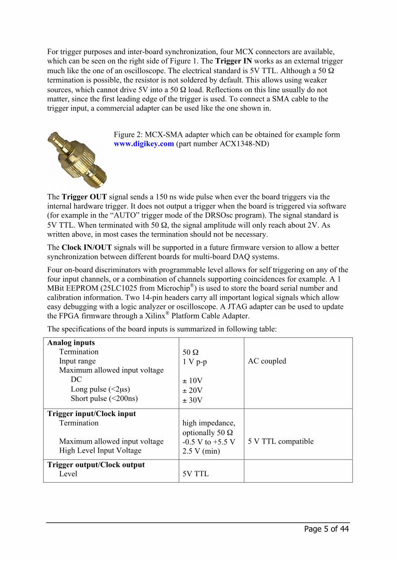
For trigger purposes and inter-board synchronization, four MCX connectors are available, which can be seen on the right side of Figure 1. The Trigger IN works as an external trigger much like the one of an oscilloscope. The electrical standard is 5V TTL. Although a 50 Ω termination is possible, the resistor is not soldered by default. This allows using weaker sources, which cannot drive 5V into a 50 Ω load. Reflections on this line usually do not matter, since the first leading edge of the trigger is used. To connect a SMA cable to the trigger input, a commercial adapter can be used like the one shown in.
Figure 2: MCX-SMA adapter which can be obtained for example form www.digikey.com (part number ACX1348-ND)
The Trigger OUT signal sends a 150 ns wide pulse when ever the board triggers via the internal hardware trigger. It does not output a trigger when the board is triggered via software (for example in the “AUTO” trigger mode of the DRSOsc program). The signal standard is 5V TTL. When terminated with 50 Ω, the signal amplitude will only reach about 2V. As written above, in most cases the termination should not be necessary. The Clock IN/OUT signals will be supported in a future firmware version to allow a better synchronization between different boards for multi-board DAQ systems. Four on-board discriminators with programmable level allows for self triggering on any of the four input channels, or a combination of channels supporting coincidences for example. A 1 MBit EEPROM (25LC1025 from Microchip®) is used to store the board serial number and calibration information. Two 14-pin headers carry all important logical signals which allow easy debugging with a logic analyzer or oscilloscope. A JTAG adapter can be used to update the FPGA firmware through a Xilinx® Platform Cable Adapter. The specifications of the board inputs is summarized in following table:
Analog inputs Termination Input range Maximum allowed input voltage DC Long pulse (<2µs) Short pulse (<200ns)
50 Ω 1 V p-p ± 10V ± 20V ± 30V
AC coupled
Trigger input/Clock input Termination Maximum allowed input voltage High Level Input Voltage
high impedance, optionally 50 Ω -0.5 V to +5.5 V 2.5 V (min)
5 V TTL compatible
Trigger output/Clock output Level
5V TTL
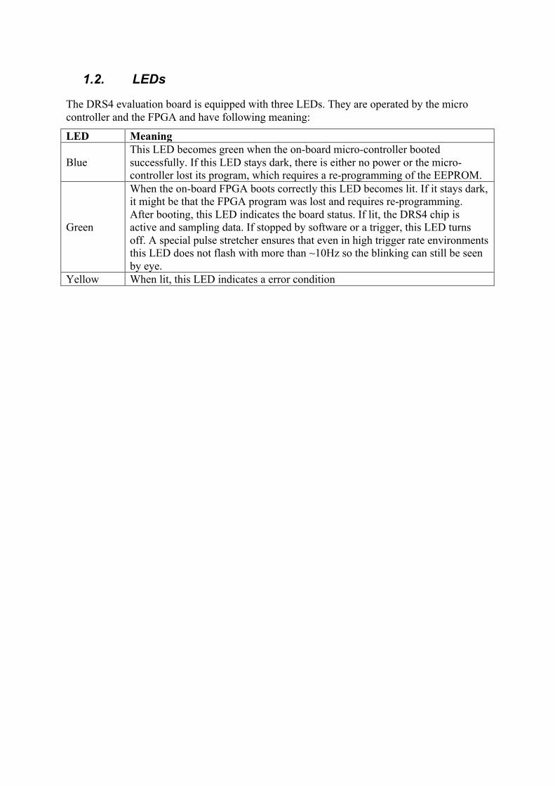
1.2. LEDs
The DRS4 evaluation board is equipped with three LEDs. They are operated by the micro controller and the FPGA and have following meaning:
LED Meaning
Blue This LED becomes green when the on-board micro-controller booted successfully. If this LED stays dark, there is either no power or the micro-controller lost its program, which requires a re-programming of the EEPROM.
Green
When the on-board FPGA boots correctly this LED becomes lit. If it stays dark, it might be that the FPGA program was lost and requires re-programming. After booting, this LED indicates the board status. If lit, the DRS4 chip is active and sampling data. If stopped by software or a trigger, this LED turns off. A special pulse stretcher ensures that even in high trigger rate environments this LED does not flash with more than ~10Hz so the blinking can still be seen by eye.
Yellow When lit, this LED indicates a error condition
Page 7 of 44
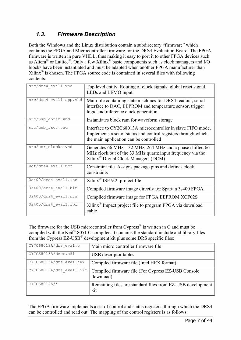
1.3. Firmware Description
Both the Windows and the Linux distribution contain a subdirectory “firmware” which contains the FPGA and Microcontroller firmware for the DRS4 Evaluation Board. The FPGA firmware is written in pure VHDL, thus making it easy to port it to other FPGA devices such as Altera® or Lattice®. Only a few Xilinx® basic components such as clock managers and I/O blocks have been instantiated and must be adapted when another FPGA manufacturer than Xilinx® is chosen. The FPGA source code is contained in several files with following contents: src/drs4_eval1.vhd Top level entity. Routing of clock signals, global reset signal,
LEDs and LEMO input src/drs4_eval1_app.vhd Main file containing state machines for DRS4 readout, serial
interface to DAC, EEPROM and temperature sensor, trigger logic and reference clock generation
src/usb_dpram.vhd Instantiates block ram for waveform storage src/usb_racc.vhd Interface to CY2C68013A microcontroller in slave FIFO mode.
Implements a set of status and control registers through which the main application can be controlled
src/usr_clocks.vhd Generates 66 MHz, 132 MHz, 264 MHz and a phase shifted 66 MHz clock out of the 33 MHz quartz input frequency via the Xilinx® Digital Clock Managers (DCM)
ucf/drs4_eval1.ucf Constraint file. Assigns package pins and defines clock constraints
3s400/drs4_eval1.ise Xilinx® ISE 9.2i project file 3s400/drs4_eval1.bit Compiled firmware image directly for Spartan 3s400 FPGA 3s400/drs4_eval1.mcs Compiled firmware image for FPGA EEPROM XCF02S 3s400/drs4_eval1.ipf Xilinx® Impact project file to program FPGA via download
cable
The firmware for the USB microcontroller from Cypress® is written in C and must be compiled with the Keil® 8051 C compiler. It contains the standard include and library files from the Cypress EZ-USB® development kit plus some DRS specific files: CY7C68013A/drs_eval.c Main micro controller firmware file CY7C68013A/dscr.a51 USB descriptor tables CY7C68013A/drs_eval.hex Compiled firmware file (Intel HEX format) CY7C68013A/drs_eval1.iic Compiled firmware file (For Cypress EZ-USB Console
download) CY7C68014A/* Remaining files are standard files from EZ-USB development
kit
The FPGA firmware implements a set of control and status registers, through which the DRS4 can be controlled and read out. The mapping of the control registers is as follows:
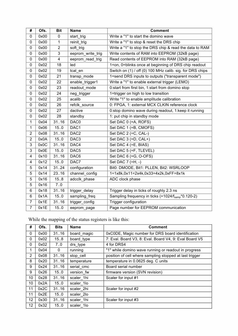
# Ofs. Bit Name Comment 0 0x00 0 start_trig Write a "1" to start the domino wave 0 0x00 1 reinit_trig Write a "1" to stop & reset the DRS chip 0 0x00 2 soft_trig Write a "1" to stop the DRS chip & read the data to RAM 0 0x00 3 eeprom_write_trig Write contents of RAM into EEPROM (32kB page) 0 0x00 4 eeprom_read_trig Read contents of EEPROM into RAM (32kB page) 0 0x02 18 led 1=on, 0=blinks once at beginning of DRS chip readout 0 0x02 19 tcal_en Switch on (1) / off (0) 100 MHz calib. sig. for DRS chips 0 0x02 21 transp_mode 1=send DRS inputs to outputs ("transparent mode") 0 0x02 22 enable_trigger1 Write a "1" to enable external trigger (LEMO) 0 0x02 23 readout_mode 0:start from first bin, 1:start from domino stop 0 0x02 24 neg_trigger 1=trigger on high to low transition 0 0x02 25 acalib Write "1" to enable amplitude calibration 0 0x02 26 refclk_source 0: FPGA, 1: external MCX CLKIN reference clock 0 0x02 27 dactive 0:stop domino wave during readout, 1:keep it running 0 0x02 28 standby 1: put chip in standby mode 1 0x04 31..16 DAC0 Set DAC 0 (=A, ROFS) 1 0x06 15..0 DAC1 Set DAC 1 (=B, CMOFS) 2 0x08 31..16 DAC2 Set DAC 2 (=C, CAL-) 2 0x0A 15..0 DAC3 Set DAC 3 (=D, CAL+) 3 0x0C 31..16 DAC4 Set DAC 4 (=E, BIAS) 3 0x0E 15..0 DAC5 Set DAC 5 (=F, TLEVEL) 4 0x10 31..16 DAC6 Set DAC 6 (=G, O-OFS) 4 0x12 15..0 DAC7 Set DAC 7 (=H, -) 5 0x14 31..24 configuration Bit0: DMODE, Bit1: PLLEN, Bit2: WSRLOOP 5 0x14 23..16 channel_config 1=1x8k,0x11=2x4k,0x33=4x2k,0xFF=8x1k 5 0x16 15..8 adcclk_phase ADC clock phase 5 0x16 7..0 6 0x18 31..16 trigger_delay Trigger delay in ticks of roughly 2.3 ns 6 0x1A 15..0 sampling_freq Sampling frequency in ticks (=1024/fsamp*0.120-2) 7 0x1E 31..16 trigger_config Trigger configuration 7 0x1E 15..0 eeprom_page Page number for EEPROM communication
While the mapping of the status registers is like this: # Ofs. Bits Name Comment 0 0x00 31..16 board_magic 0xC0DE, Magic number for DRS board identification 0 0x02 15..8 board_type 7: Eval. Board V3, 8: Eval. Board V4, 9: Eval Board V5 0 0x02 7..0 drs_type 4 for DRS4 1 0x04 0 running "1" while domino wave running or readout in progress 2 0x08 31..16 stop_cell position of cell where sampling stopped at last trigger 8 0x20 31..16 temperature temperature in 0.0625 deg. C units 9 0x24 31..16 serial_cmc Board serial number 9 0x26 15..0 version_fw firmware version (SVN revision)
10 0x28 31..16 scaler_1hi Scaler for input #1 10 0x2A 15..0 scaler_1lo 11 0x2C 31..16 scaler_2hi Scaler for input #2 11 0x2E 15..0 scaler_2lo 12 0x30 31..16 scaler_1hi Scaler for input #3 12 0x32 15..0 scaler_1lo
Page 9 of 44
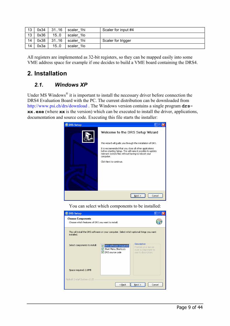
13 0x34 31..16 scaler_1hi Scaler for input #4 13 0x36 15..0 scaler_1lo 14 0x38 31..16 scaler_1hi Scaler for trigger 14 0x3a 15..0 scaler_1lo All registers are implemented as 32-bit registers, so they can be mapped easily into some VME address space for example if one decides to build a VME board containing the DRS4.
2. Installation
2.1. Windows XP
Under MS Windows® it is important to install the necessary driver before connection the DRS4 Evaluation Board with the PC. The current distribution can be downloaded from http://www.psi.ch/drs/download . The Windows version contains a single program drs-xx.exe (where xx is the version) which can be executed to install the driver, applications, documentation and source code. Executing this file starts the installer:
You can select which components to be installed:
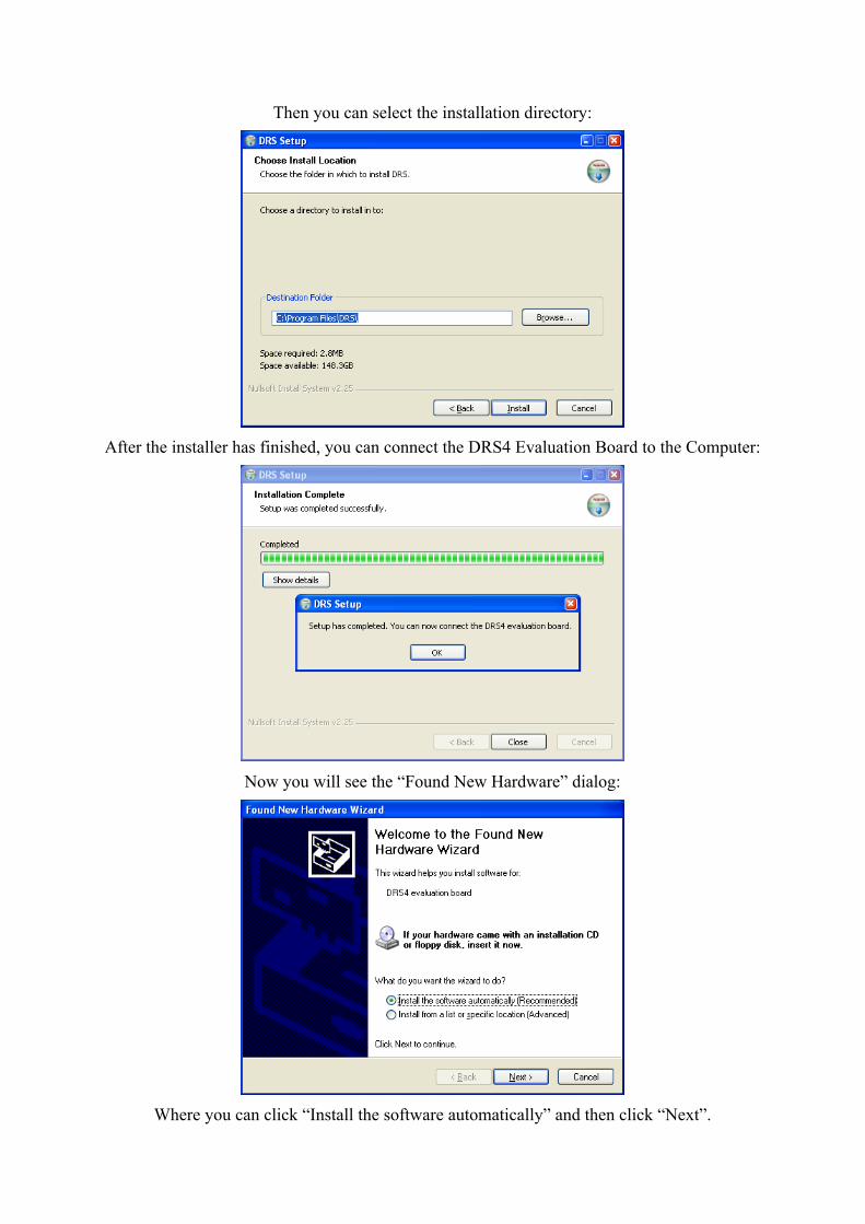
Then you can select the installation directory:
After the installer has finished, you can connect the DRS4 Evaluation Board to the Computer:
Now you will see the “Found New Hardware” dialog:
Where you can click “Install the software automatically” and then click “Next”.
Page 11 of 44
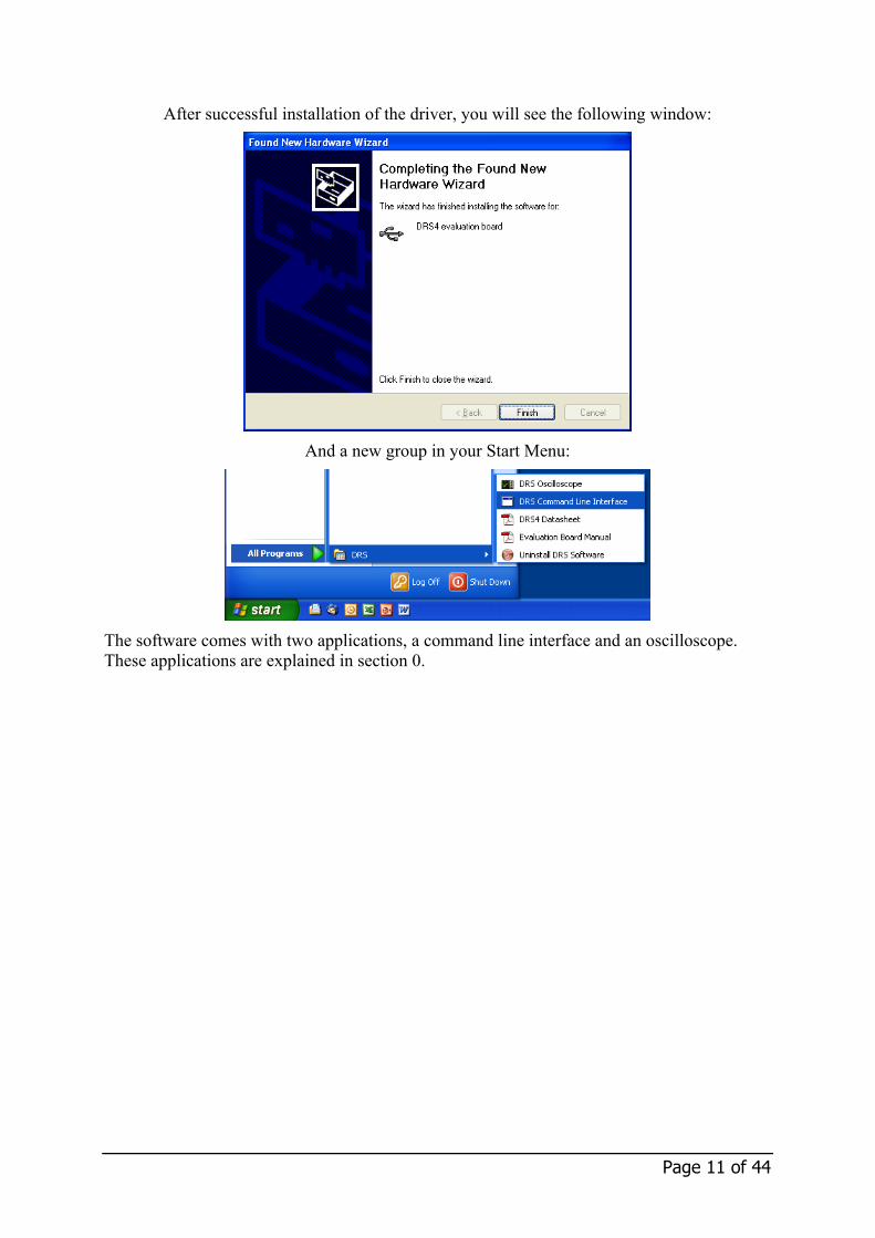
After successful installation of the driver, you will see the following window:
And a new group in your Start Menu:
The software comes with two applications, a command line interface and an oscilloscope. These applications are explained in section 0.
2.2. Windows 7
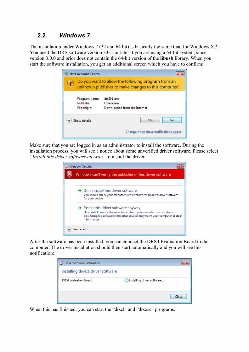
The installation under Windows 7 (32 and 64 bit) is basically the same than for Windows XP. You need the DRS software version 3.0.1 or later if you are using a 64-bit system, since version 3.0.0 and prior does not contain the 64-bit version of the libusb library. When you start the software installation, you get an additional screen which you have to confirm:
Make sure that you are logged in as an administrator to install the software. During the installation process, you will see a notice about some unverified driver software. Please select “Install this driver software anyway” to install the driver.
After the software has been installed, you can connect the DRS4 Evaluation Board to the computer. The driver installation should then start automatically and you will see this notification:
When this has finished, you can start the “drscl” and “drsosc” programs.
Page 13 of 44
2.3. Upgrading from software
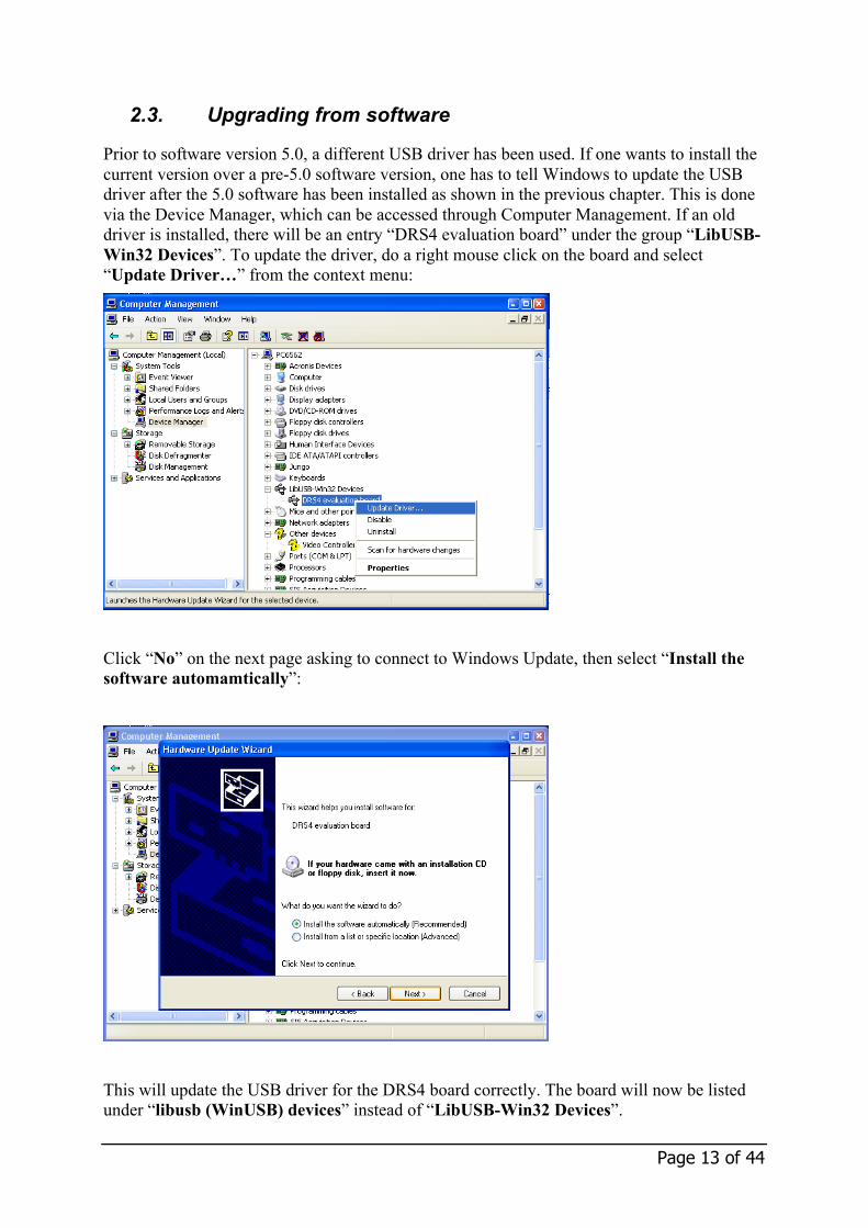
Prior to software version 5.0, a different USB driver has been used. If one wants to install the current version over a pre-5.0 software version, one has to tell Windows to update the USB driver after the 5.0 software has been installed as shown in the previous chapter. This is done via the Device Manager, which can be accessed through Computer Management. If an old driver is installed, there will be an entry “DRS4 evaluation board” under the group “LibUSB-Win32 Devices”. To update the driver, do a right mouse click on the board and select “Update Driver…” from the context menu:
Click “No” on the next page asking to connect to Windows Update, then select “Install the software automamtically”:
This will update the USB driver for the DRS4 board correctly. The board will now be listed under “libusb (WinUSB) devices” instead of “LibUSB-Win32 Devices”.
2.4. Linux
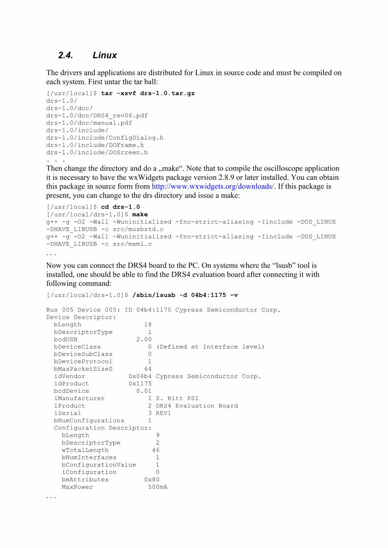
The drivers and applications are distributed for Linux in source code and must be compiled on each system. First untar the tar ball: [/usr/local]$ tar -xzvf drs-1.0.tar.gz drs-1.0/ drs-1.0/doc/ drs-1.0/doc/DRS4_rev06.pdf drs-1.0/doc/manual.pdf drs-1.0/include/ drs-1.0/include/ConfigDialog.h drs-1.0/include/DOFrame.h drs-1.0/include/DOScreen.h . . .
Then change the directory and do a „make“. Note that to compile the oscilloscope application it is necessary to have the wxWidgets package version 2.8.9 or later installed. You can obtain this package in source form from http://www.wxwidgets.org/downloads/. If this package is present, you can change to the drs directory and issue a make: [/usr/local]$ cd drs-1.0 [/usr/local/drs-1.0]$ make g++ -g -O2 -Wall -Wuninitialized -fno-strict-aliasing -Iinclude -DOS_LINUX -DHAVE_LIBUSB -c src/musbstd.c g++ -g -O2 -Wall -Wuninitialized -fno-strict-aliasing -Iinclude -DOS_LINUX -DHAVE_LIBUSB -c src/mxml.c
. . . Now you can connect the DRS4 board to the PC. On systems where the “lsusb” tool is installed, one should be able to find the DRS4 evaluation board after connecting it with following command: [/usr/local/drs-1.0]$ /sbin/lsusb -d 04b4:1175 –v Bus 005 Device 005: ID 04b4:1175 Cypress Semiconductor Corp. Device Descriptor: bLength 18 bDescriptorType 1 bcdUSB 2.00 bDeviceClass 0 (Defined at Interface level) bDeviceSubClass 0 bDeviceProtocol 1 bMaxPacketSize0 64 idVendor 0x04b4 Cypress Semiconductor Corp. idProduct 0x1175 bcdDevice 0.01 iManufacturer 1 S. Ritt PSI iProduct 2 DRS4 Evaluation Board iSerial 3 REV1 bNumConfigurations 1 Configuration Descriptor: bLength 9 bDescriptorType 2 wTotalLength 46 bNumInterfaces 1 bConfigurationValue 1 iConfiguration 0 bmAttributes 0x80 MaxPower 500mA
. . .
Page 15 of 44
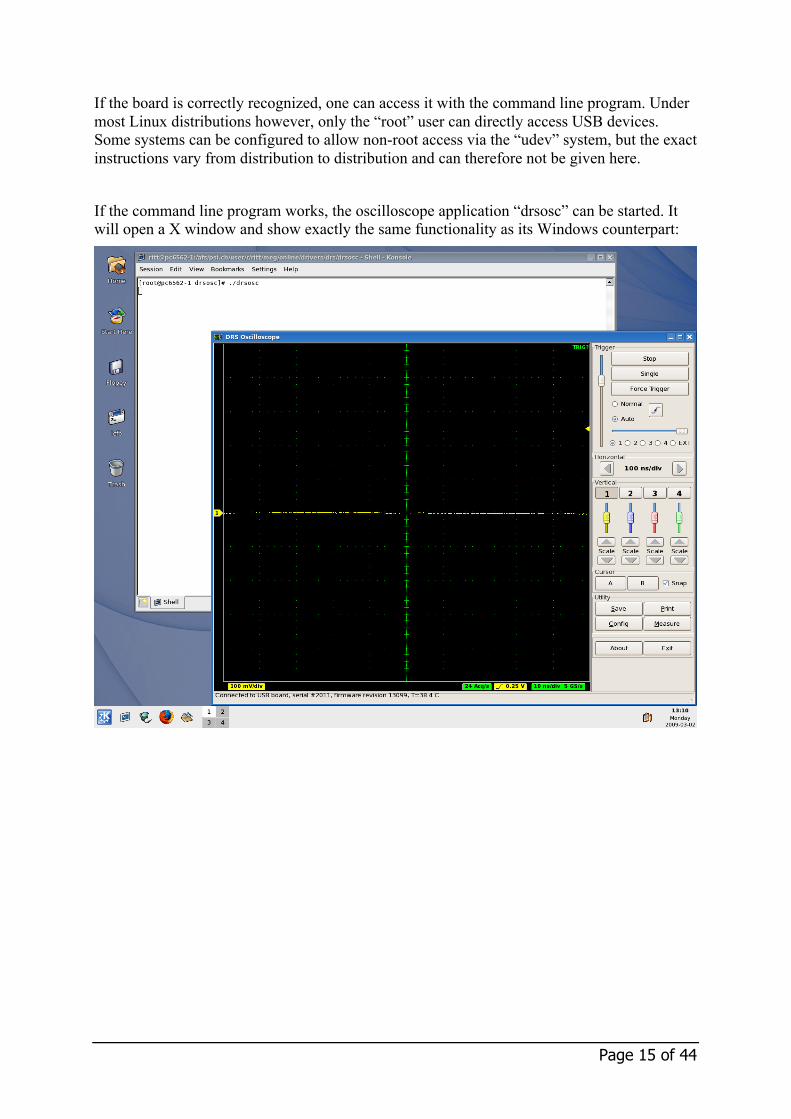
If the board is correctly recognized, one can access it with the command line program. Under most Linux distributions however, only the “root” user can directly access USB devices. Some systems can be configured to allow non-root access via the “udev” system, but the exact instructions vary from distribution to distribution and can therefore not be given here.
If the command line program works, the oscilloscope application “drsosc” can be started. It will open a X window and show exactly the same functionality as its Windows counterpart:
2.5. Macintosh OSX
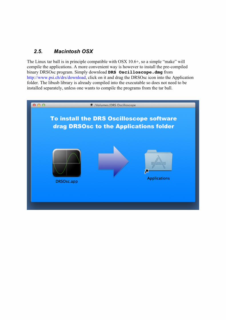
The Linux tar ball is in principle compatible with OSX 10.6+, so a simple “make” will compile the applications. A more convenient way is however to install the pre-compiled binary DRSOsc program. Simply download DRS Oscilloscope.dmg from http://www.psi.ch/drs/download, click on it and drag the DRSOsc icon into the Application folder. The libusb library is already compiled into the executable so does not need to be installed separately, unless one wants to compile the programs from the tar ball.
Page 17 of 44
3. Running the Board
3.1. Command line Interface “drscl”
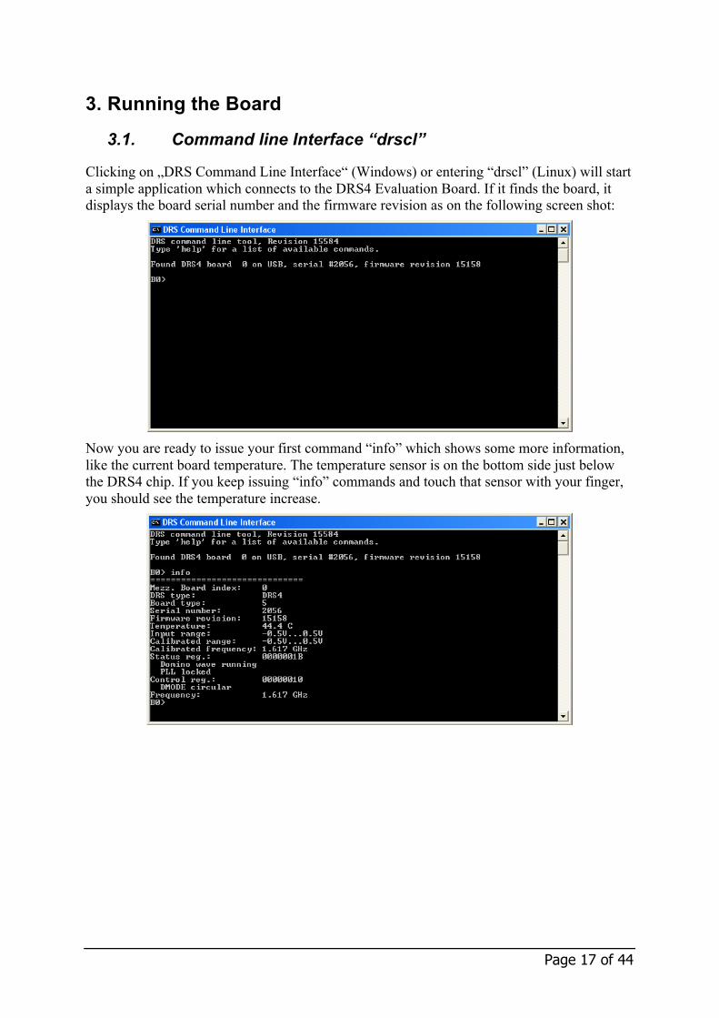
Clicking on „DRS Command Line Interface“ (Windows) or entering “drscl” (Linux) will start a simple application which connects to the DRS4 Evaluation Board. If it finds the board, it displays the board serial number and the firmware revision as on the following screen shot:
Now you are ready to issue your first command “info” which shows some more information, like the current board temperature. The temperature sensor is on the bottom side just below the DRS4 chip. If you keep issuing “info” commands and touch that sensor with your finger, you should see the temperature increase.
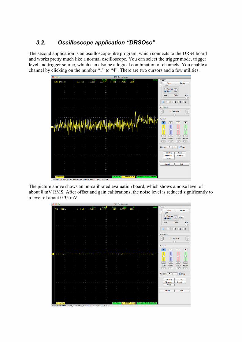
3.2. Oscilloscope application “DRSOsc”
The second application is an oscilloscope-like program, which connects to the DRS4 board and works pretty much like a normal oscilloscope. You can select the trigger mode, trigger level and trigger source, which can also be a logical combination of channels. You enable a channel by clicking on the number “1” to “4”. There are two cursors and a few utilities.
The picture above shows an un-calibrated evaluation board, which shows a noise level of about 8 mV RMS. After offset and gain calibrations, the noise level is reduced significantly to a level of about 0.35 mV:
Page 19 of 44
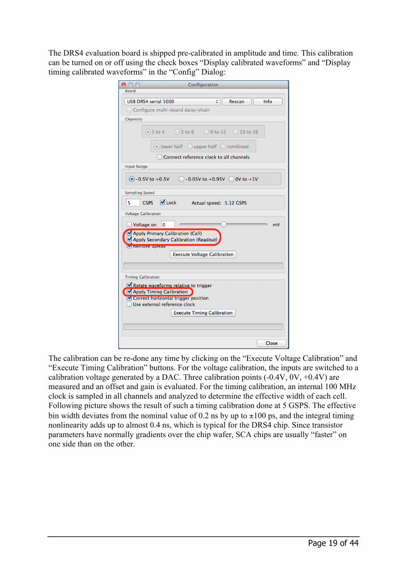
The DRS4 evaluation board is shipped pre-calibrated in amplitude and time. This calibration can be turned on or off using the check boxes “Display calibrated waveforms” and “Display timing calibrated waveforms” in the “Config” Dialog:
The calibration can be re-done any time by clicking on the “Execute Voltage Calibration” and “Execute Timing Calibration” buttons. For the voltage calibration, the inputs are switched to a calibration voltage generated by a DAC. Three calibration points (-0.4V, 0V, +0.4V) are measured and an offset and gain is evaluated. For the timing calibration, an internal 100 MHz clock is sampled in all channels and analyzed to determine the effective width of each cell. Following picture shows the result of such a timing calibration done at 5 GSPS. The effective bin width deviates from the nominal value of 0.2 ns by up to ±100 ps, and the integral timing nonlinearity adds up to almost 0.4 ns, which is typical for the DRS4 chip. Since transistor parameters have normally gradients over the chip wafer, SCA chips are usually “faster” on one side than on the other.
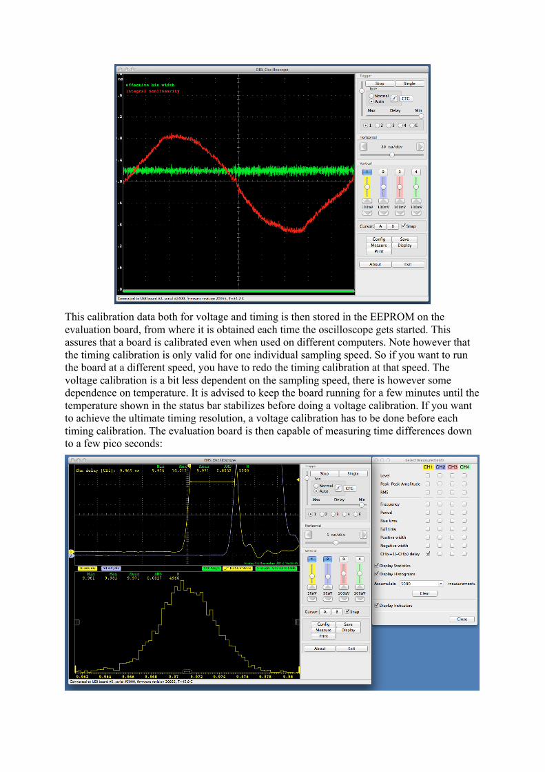
This calibration data both for voltage and timing is then stored in the EEPROM on the evaluation board, from where it is obtained each time the oscilloscope gets started. This assures that a board is calibrated even when used on different computers. Note however that the timing calibration is only valid for one individual sampling speed. So if you want to run the board at a different speed, you have to redo the timing calibration at that speed. The voltage calibration is a bit less dependent on the sampling speed, there is however some dependence on temperature. It is advised to keep the board running for a few minutes until the temperature shown in the status bar stabilizes before doing a voltage calibration. If you want to achieve the ultimate timing resolution, a voltage calibration has to be done before each timing calibration. The evaluation board is then capable of measuring time differences down to a few pico seconds:
Page 21 of 44
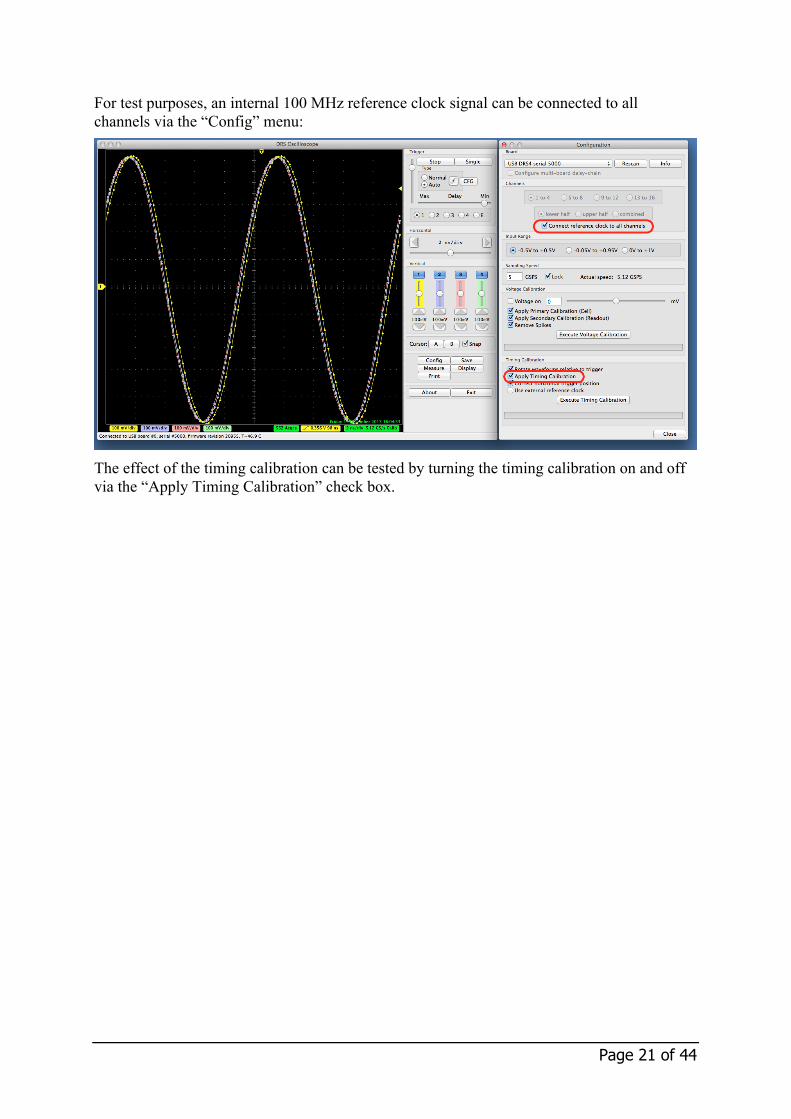
For test purposes, an internal 100 MHz reference clock signal can be connected to all channels via the “Config” menu:
The effect of the timing calibration can be tested by turning the timing calibration on and off via the “Apply Timing Calibration” check box.
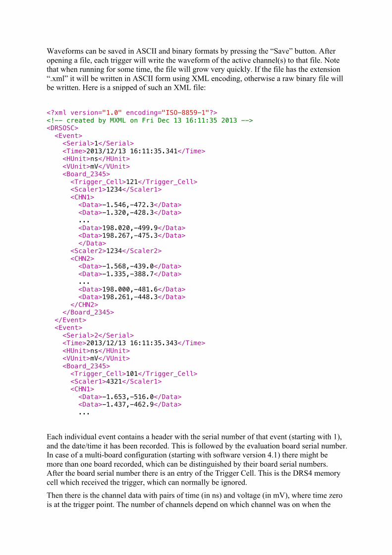
Waveforms can be saved in ASCII and binary formats by pressing the “Save” button. After opening a file, each trigger will write the waveform of the active channel(s) to that file. Note that when running for some time, the file will grow very quickly. If the file has the extension “.xml” it will be written in ASCII form using XML encoding, otherwise a raw binary file will be written. Here is a snipped of such an XML file:
<?xml version="1.0" encoding="ISO-8859-1"?> <!-- created by MXML on Fri Dec 13 16:11:35 2013 --> <DRSOSC> <Event> <Serial>1</Serial> <Time>2013/12/13 16:11:35.341</Time> <HUnit>ns</HUnit> <VUnit>mV</VUnit> <Board_2345> <Trigger_Cell>121</Trigger_Cell> <Scaler1>1234</Scaler1> <CHN1> <Data>-1.546,-472.3</Data> <Data>-1.320,-428.3</Data> ... <Data>198.020,-499.9</Data> <Data>198.267,-475.3</Data> </Data> <Scaler2>1234</Scaler2> <CHN2> <Data>-1.568,-439.0</Data> <Data>-1.335,-388.7</Data> ... <Data>198.000,-481.6</Data> <Data>198.261,-448.3</Data> </CHN2> </Board_2345> </Event> <Event> <Serial>2</Serial> <Time>2013/12/13 16:11:35.343</Time> <HUnit>ns</HUnit> <VUnit>mV</VUnit> <Board_2345> <Trigger_Cell>101</Trigger_Cell> <Scaler1>4321</Scaler1> <CHN1> <Data>-1.653,-516.0</Data> <Data>-1.437,-462.9</Data> ...
Each individual event contains a header with the serial number of that event (starting with 1), and the date/time it has been recorded. This is followed by the evaluation board serial number. In case of a multi-board configuration (starting with software version 4.1) there might be more than one board recorded, which can be distinguished by their board serial numbers. After the board serial number there is an entry of the Trigger Cell. This is the DRS4 memory cell which received the trigger, which can normally be ignored. Then there is the channel data with pairs of time (in ns) and voltage (in mV), where time zero is at the trigger point. The number of channels depend on which channel was on when the
Page 23 of 44
data was recorded. It might be a single channel (CHN1) or all four channels (CHN1-CHN4). Please note that the XML format requires more hard disk space compared to the binary format and takes also more CPU power to be written, so the maximum data rate is limited.
The binary format requires less space and can be written faster, but it requires a special program to read and analyze the data afterwards. Depending on the number of channels that are “on” during data acquisition, the file contains up to four channels for each evaluation board, which can be identified by their channel headers. In a multi-board setup (starting with software version 4.1) there can be more than one board per event. In this case there are several board blocks with different board serial numbers.
At the beginning of each file there is a section that contains the timing calibration of one or more boards. In the DRS4 chip, the “width” of each sampling bin is different, and therefore needs to be measured and calibrated. This timing calibration is stored inside the EEPROM of each evaluation board. The timing section at the beginning of the binary file contains a copy of this timing calibration. Since it is constant over time, it is valid for all events in the file and is not repeated for each event in order to save space. Starting with the V5 board, each channel has its own calibration. Depending which channels were turned on during acquisition, there might be 1-4 timing calibration arrays, which can be seen from the channel headers.
One problem however is that in each event the readout starts at a different position of the DRS4 chip (the so-called “trigger cell”). Unlike in the XML format, the voltage/time pairs have to be calculated for each event individually. If the array dtch[1024] contains the effective bin widths of a channel ch of the DRS4 chip obtained from the binary file, the time tch[i] belonging to sample i can be calculated using the trigger cell tcell as follows:
tch[i]= dtch[( j + tcell)%1024]j=0
i−1
∑
where % is the modulo operator. The time array starts with tch[0]=0. Another complication comes from the fact that the timing of the channels in a DRS chip is different. So a given cell i has a different absolute time in each channel. The only common point in time is cell #0 (the first cell in the capacitor array), which has the same absolute time in all DRS channels. To obtain best timing, it is therefore necessary to align all channels such that their cell #0 has the same time tch,0 as given by
tch,0 = tch[(1024− tcell)%1024]
If channel 1 is used as the reference point, the time arrays of the other channels can be shifted so that their cell #0 aligns:
tch[i]corrected = tch[i]− (tch,0 − t0,0 )
The distribution contains a file read_binary.cpp, which reads the binary data format produced by DRSOsc and calculates the correct times as described above. It can be used as an example program to analyze binary waveform data. The timing calibration section is followed by the actual waveform data. Each event can be identified by the event header ‘EHDR’, which is followed by one or more arrays of sampling values, depending on what channel was enabled during the acquisition. The voltage values are encoded as 2-byte integers, were 0 corresponds to -0.5V and 65535 corresponds to +0.5V. All multi-byte data is encoded with LSB first, as in all Intel PC systems.
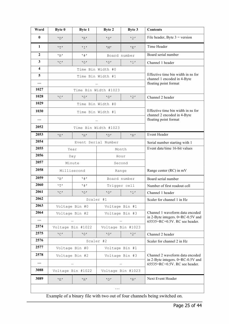
Page 25 of 44
Word Byte 0 Byte 1 Byte 2 Byte 3 Contents
0 ‘D’ ‘R’ ‘S’ ‘2’ File header, Byte 3 = version
1 ‘T’ ‘I’ ‘M’ ‘E’ Time Header
2 ‘B’ ‘#’ Board number Board serial number
3 ‘C’ ‘0’ ‘0’ ‘1’ Channel 1 header 4 Time Bin Width #0
Effective time bin width in ns for channel 1 encoded in 4-Byte floating point format
5 Time Bin Width #1
… …
1027 Time Bin Width #1023
1028 ‘C’ ‘0’ ‘0’ ‘2’ Channel 2 header 1029 Time Bin Width #0
Effective time bin width in ns for channel 2 encoded in 4-Byte floating point format
1030 Time Bin Width #1
… …
2052 Time Bin Width #1023
2053 ‘E’ ‘H’ ‘D’ ‘R’ Event Header
2054 Event Serial Number Serial number starting with 1 2055 Year Month Event date/time 16-bit values
Range center (RC) in mV
2056 Day Hour
2057 Minute Second
2058 Millisecond Range
2059 ‘B’ ‘#’ Board number Board serial number 2060 ‘T’ ‘#’ Trigger cell Number of first readout cell 2061 ‘C’ ‘0’ ‘0’ ‘1’ Channel 1 header 2062 Scaler #1 Scaler for channel 1 in Hz 2063 Voltage Bin #0 Voltage Bin #1
Channel 1 waveform data encoded in 2-Byte integers. 0=RC-0.5V and 65535=RC+0.5V. RC see header.
2064 Voltage Bin #2 Voltage Bin #3
… … …
2574 Voltage Bin #1022 Voltage Bin #1023
2575 ‘C’ ‘0’ ‘0’ ‘2’ Channel 2 header 2576 Scaler #2 Scaler for channel 2 in Hz 2577 Voltage Bin #0 Voltage Bin #1
Channel 2 waveform data encoded in 2-Byte integers. 0=RC-0.5V and 65535=RC+0.5V. RC see header.
2578 Voltage Bin #2 Voltage Bin #3
… … …
3088 Voltage Bin #1022 Voltage Bin #1023
3089 ‘E’ ‘H’ ‘D’ ‘R’ Next Event Header
…
Example of a binary file with two out of four channels being switched on.
3.3. Multi-board configuration
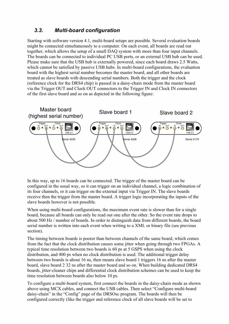
Starting with software version 4.1, multi-board setups are possible. Several evaluation boards might be connected simultaneously to a computer. On each event, all boards are read out together, which allows the setup of a small DAQ system with more than four input channels. The boards can be connected to individual PC USB ports, or an external USB hub can be used. Please make sure that the USB hub is externally powered, since each board draws 2.5 Watts, which cannot be satisfied by passive USB hubs. In multi-board configurations, the evaluation board with the highest serial number becomes the master board, and all other boards are treated as slave boards with descending serial numbers. Both the trigger and the clock (reference clock for the DRS4 chip) is passed in a daisy-chain mode from the master board via the Trigger OUT and Clock OUT connectors to the Trigger IN and Clock IN connectors of the first slave board and so on as depicted in the following figure:
TriggerIN OUT IN OUT
Clock
USB 2.0
TriggerIN OUT IN OUT
Clock
USB 2.0
TriggerIN OUT IN OUT
Clock
USB 2.0
Master board(highest serial number) Slave board 1 Slave board 2
Serial 4230 Serial 4228 Serial 4170
In this way, up to 16 boards can be connected. The trigger of the master board can be configured in the usual way, so it can trigger on an individual channel, a logic combination of its four channels, or it can trigger on the external input via Trigger IN. The slave boards receive then the trigger from the master board. A trigger logic incorporating the inputs of the slave boards however is not possible.
When using multi-board configurations, the maximum event rate is slower than for a single board, because all boards can only be read out one after the other. So the event rate drops to about 500 Hz / number of boards. In order to distinguish data from different boards, the board serial number is written into each event when writing to a XML or binary file (see previous section). The timing between boards is poorer than between channels of the same board, which comes from the fact that the clock distribution causes some jitter when going through two FPGAs. A typical time resolution between two boards is 60 ps at 5 GSPS when using the clock distribution, and 400 ps when no clock distribution is used. The additional trigger delay between two boards is about 16 ns, then means slave board 1 triggers 16 ns after the master board, slave board 2 32 ns after the master board and so on. When building dedicated DRS4 boards, jitter-cleaner chips and differential clock distribution schemes can be used to keep the time resolution between boards also below 10 ps. To configure a multi-board system, first connect the boards in the daisy-chain mode as shown above using MCX cables, and connect the USB cables. Then select “Configure multi-board daisy-chain” in the “Config” page of the DRSOsc program. The boards will then be configured correctly (like the trigger and reference clock of all slave boards will be set to
Page 27 of 44
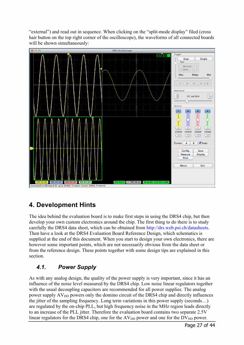
“external”) and read out in sequence. When clicking on the “split-mode display” filed (cross hair button on the top right corner of the oscilloscope), the waveforms of all connected boards will be shown simultaneously:
4. Development Hints The idea behind the evaluation board is to make first steps in using the DRS4 chip, but then develop your own custom electronics around the chip. The first thing to do there is to study carefully the DRS4 data sheet, which can be obtained from http://drs.web.psi.ch/datasheets. Then have a look at the DRS4 Evaluation Board Reference Design, which schematics is supplied at the end of this document. When you start to design your own electronics, there are however some important points, which are not necessarily obvious from the data sheet or from the reference design. These points together with some design tips are explained in this section.
4.1. Power Supply
As with any analog design, the quality of the power supply is very important, since it has an influence of the noise level measured by the DRS4 chip. Low noise linear regulators together with the usual decoupling capacitors are recommended for all power supplies. The analog power supply AVDD powers only the domino circuit of the DRS4 chip and directly influences the jitter of the sampling frequency. Long term variations in this power supply (seconds…) are regulated by the on-chip PLL, but high frequency noise in the MHz region leads directly to an increase of the PLL jitter. Therefore the evaluation board contains two separate 2.5V linear regulators for the DRS4 chip, one for the AVDD power and one for the DVDD power.
Although the DVDD power is called “digital power”, it powers also the analog output buffers of the DRS4 chip and needs the same good quality than the AVDD power in order to minimize the noise of the board.
The DRS4 chip also contains two grounds AGND and DGND. They can be either routed separately on the board and be connected at the power source, or they can be directly connected to an overall dedicated ground plane of the PCB. Tests have been shown that the latter choice gives slightly less noise.
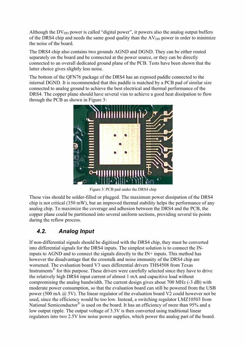
The bottom of the QFN76 package of the DRS4 has an exposed paddle connected to the internal DGND. It is recommended that this paddle is matched by a PCB pad of similar size connected to analog ground to achieve the best electrical and thermal performance of the DRS4. The copper plane should have several vias to achieve a good heat dissipation to flow through the PCB as shown in Figure 3:
Figure 3: PCB pad under the DRS4 chip
These vias should be solder-filled or plugged. The maximum power dissipation of the DRS4 chip is not critical (350 mW), but an improved thermal stability helps the performance of any analog chip. To maximize the coverage and adhesion between the DRS4 and the PCB, the copper plane could be partitioned into several uniform sections, providing several tie points during the reflow process.
4.2. Analog Input
If non-differential signals should be digitized with the DRS4 chip, they must be converted into differential signals for the DRS4 inputs. The simplest solution is to connect the IN- inputs to AGND and to connect the signals directly to the IN+ inputs. This method has however the disadvantage that the crosstalk and noise immunity of the DRS4 chip are worsened. The evaluation board V3 uses differential drivers THS4508 from Texas Instruments® for this purpose. These drivers were carefully selected since they have to drive the relatively high DRS4 input current of almost 1 mA and capacitive load without compromising the analog bandwidth. The current design gives about 700 MHz (-3 dB) with moderate power consumption, so that the evaluation board can still be powered from the USB power (500 mA @ 5V). The linear regulator of the evaluation board V2 could however not be used, since the efficiency would be too low. Instead, a switching regulator LMZ10503 from National Semiconductor® is used on the board. It has an efficiency of more than 95% and a low output ripple. The output voltage of 3.3V is then converted using traditional linear regulators into two 2.5V low noise power supplies, which power the analog part of the board.
Page 29 of 44
Other designs are possible which push the analog bandwidth to 800 or 900 MHz, close to the theoretical limit of 950 MHz of the DRS4 chip, but they require more power. The usual design rules like proper termination, matched impedance PCB traces and separate power supply PCB planes apply as in any high frequency analog design.
4.3. Control Voltages
The DRS4 chip requires certain control voltages: ROFS, O-OFS and BIAS. The latter two are generated internally with some default voltage, but can be “overwritten” by an external low impedance source. It is recommended to connect these lines to an external 16-bit DAC, so that the DRS4 input range can be fine-tuned on a board-by-board basis, to compensate for chip variations. The ROFS signal should be driven by a high speed low noise buffer. If this signal would be directly connected to the DAC output, the signal height would change slightly during the chip readout and the measurement would show a varying baseline level.
4.4. ADC Clock
There is a very strict relation between the DRS4 output shift register clock SRCLK and the ADC clock (see DRS4 data sheet WAVEFORM READOUT). In order to reduce the noise due to aperture jitter, the phase shift between these two clocks must be fixed and contain very small jitter (~10ps). The easiest way to generate this phase shift is to use the digital clock managers (DCM) in the FPGA, as it is done on the evaluation board. Since the DCMs have however an inherent phase jitter of up to 150ps, this introduces some noise in form of a baseline variation when sampling a DC signal in the order of up to a few mV. If this becomes a problem, it is recommended to generate the phase shift between these two clocks with a low jitter delay circuit.
4.5. Calibration
In order to perform a proper voltage calibration of the DRS4 chip, a well-defined DC voltage needs to be connected to all DRS4 inputs and measured. The evaluation board uses the on-board 16-bit DAC connected to all inputs for that purpose. Since the DRS4 chip draws quite some current on its inputs, the DAC is buffered via a low noise OpAmp AD8605.
For the timing calibration, a low jitter 100 MHz sine wave needs to be connected to all channels. In evaluation boards previous to version 5, only one DRS4 channel was connected to the clock, which allows timing calibrations good for about 10-15 ps. To achieve the ultimate resolution below 3 ps, the clock needs to be connected to all DRS4 channels via analog switches. The sine wave is obtained from a low jitter quartz oscillator with a passive 3rd order low pass filter. Since the oscillator would cause some noise during normal operation, it can be disabled through the FPGA.
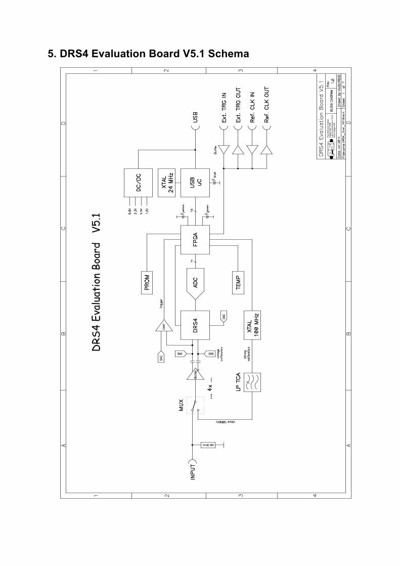
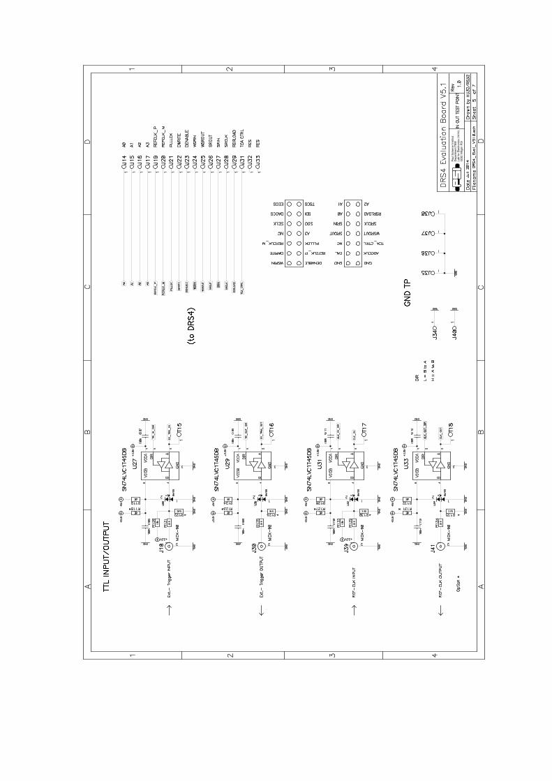
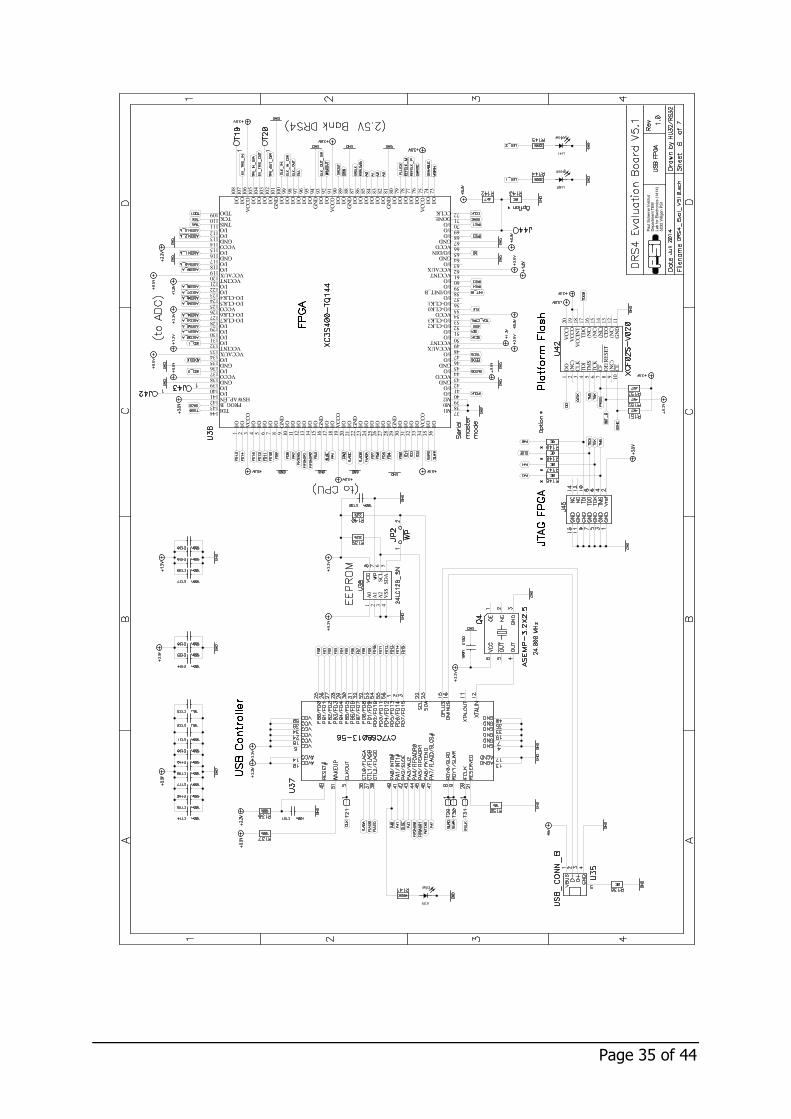
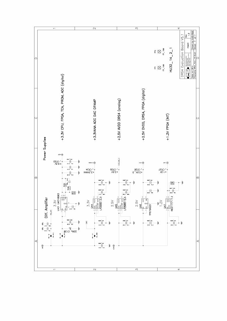
5. DRS4 Evaluation Board V5.1 Schema
Depa
rtmen
t TEM
Lab
for E
lect
roni
cs (1
414)
5232
Villi
gen
PSI
Paul
Sch
erre
r Ins
titut
DRS
4 Ev
alua
tion
Boa
rd
V5.1
Page 31 of 44
Depa
rtmen
t TEM
Lab
for E
lect
roni
cs (1
414)
5232
Villi
gen
PSI
Paul
Sch
erre
r Ins
titut
35 4
BAV99S
621
621
35 4
BAV99S
621
621
35 4
BAV99S3
5 4
BAV99S
4Y
3GND
5VCC
2A
1NC
Depa
rtmen
t TEM
Lab
for E
lect
roni
cs (1
414)
5232
Villi
gen
PSI
Paul
Sch
erre
r Ins
titut
4 3
6 2
1
4 3
6 2
1
4 3
6 2
1
4 3
6 2
14
Y3GND
5VCC
2A
1NC
Page 33 of 44
Depa
rtmen
t TEM
Lab
for E
lect
roni
cs (1
414)
5232
Villi
gen
PSI
Paul
Sch
erre
r Ins
titut
3WP
2SO
4VSS
1CS
6SCK
5SI
5
4
2
31
5
4
23
15
4
2
31
5
4
2
31
Depa
rtmen
t TEM
Lab
for E
lect
roni
cs (1
414)
5232
Villi
gen
PSI
Paul
Sch
erre
r Ins
titut
Page 35 of 44
Depa
rtmen
t TEM
Lab
for E
lect
roni
cs (1
414)
5232
Villi
gen
PSI
Paul
Sch
erre
r Ins
titut
3A2
4VSS
1A0
2A1
6SCL
5SDA
11GND
14(NC)
17TDO
20VCCJ
13CEO12
(NC)
19VCCO
18VCCINT16
(NC)
15(NC)
10CE
7CF
4TDI
1DO
8OE/RESET
9(NC)
2(NC)
3CLK
5TMS
6TCK
39M2
42GND139 GND
45GND136 GND
51I/O130 I/O
57I/O
60I/O
63I/O118 I/O
69I/O112 I/O
109 TDO
142 HSWAP_EN
48VCCAUX133 VCCINT
54VCCO127 I/O-CLK6
124 I/O-CLK4
121 VCCINT
66VCCO115 VCCO
72CCLK
31I/O
28I/O
25I/O
13I/O
10I/O
7I/O
4I/O
1I/O
75VCCO
78I/O
81GND
84I/O
87I/O
90I/O
93I/O
96I/O
99I/O
102
I/O
105
I/O
108
I/O
33I/O
30I/O
27I/O
32I/O
26I/O
35I/O
21I/O
18I/O
15I/O
20I/O
17I/O
14I/O
23I/O
6I/O
8I/O
5I/O
2I/O
11I/O
37M1
40I/O
46I/O
41I/O
44I/O
38M0141 I/O
135 I/O
144 TDI
137 I/O
140 I/O
50I/O132 I/O
129 I/O
123 I/O
131 I/O
64GND
67GND
70I/O
68I/O
117 GND
114 GND
111 TMS
113 I/O
119 I/O
116 I/O
76I/O
79I/O
82I/O
77I/O
80I/O
83I/O
74I/O
88GND
94GND
89I/O
92I/O
95I/O
86I/O
91VCCO
100
I/O
103
I/O101
GND
104
I/O
107
I/O
98I/O
106
VCCO
36I/O
24I/O
12I/O
43VCCO138 VCCO
143 PROG_B
49VCCINT
52I/O-CLK2
55I/O-CLK0
58I/O/INIT_B
56I/O-CLK1
53I/O-CLK3126 VCCO125
I/O-CLK5
128 I/O-CLK7
61VCCINT62VCCAUX
65I/O/DIN
120 VCCAUX
73I/O
85I/O
97I/O
34VCCO
22GND
19VCCO
16GND
47I/O
29GND
9GND
3VCCO
59I/O122 I/O
110 TCK
134 VCCAUX
71DONE
Depa
rtmen
t TEM
Lab
for E
lect
roni
cs (1
414)
5232
Villi
gen
PSI
Paul
Sch
erre
r Ins
titut
1VIN
5VOUT
3ON/OFF
2GND
4BYP
1VIN
5VOUT
3ON/OFF
2GND
4BYP
3GND
2IN
1EN
4OUT
5NR
2OUT
4OUT
3IN
1GND3SS
4GND
6OUT
7OUT
5FB
2EN
1IN
Page 37 of 44
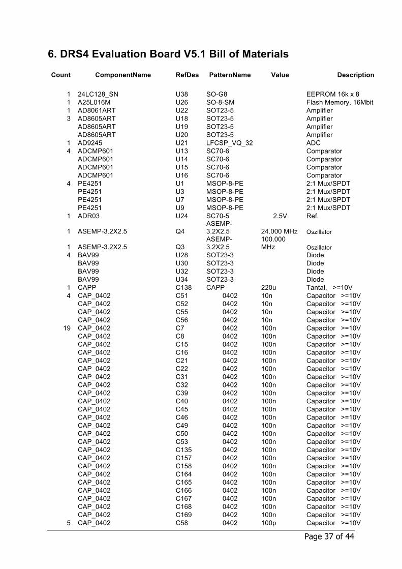
6. DRS4 Evaluation Board V5.1 Bill of Materials
Count ComponentName RefDes PatternName Value Description
1 24LC128_SN U38 SO-G8 EEPROM 16k x 8 1 A25L016M U26 SO-8-SM Flash Memory, 16Mbit 1 AD8061ART U22 SOT23-5 Amplifier 3 AD8605ART U18 SOT23-5 Amplifier
AD8605ART U19 SOT23-5 Amplifier AD8605ART U20 SOT23-5 Amplifier
1 AD9245 U21 LFCSP_VQ_32 ADC 4 ADCMP601 U13 SC70-6 Comparator
ADCMP601 U14 SC70-6 Comparator ADCMP601 U15 SC70-6 Comparator ADCMP601 U16 SC70-6 Comparator
4 PE4251 U1 MSOP-8-PE 2:1 Mux/SPDT PE4251 U3 MSOP-8-PE 2:1 Mux/SPDT PE4251 U7 MSOP-8-PE 2:1 Mux/SPDT PE4251 U9 MSOP-8-PE 2:1 Mux/SPDT
1 ADR03 U24 SC70-5 2.5V Ref.
1 ASEMP-3.2X2.5 Q4 ASEMP-3.2X2.5 24.000 MHz Oszillator
1 ASEMP-3.2X2.5 Q3 ASEMP-3.2X2.5
100.000 MHz Oszillator
4 BAV99 U28 SOT23-3 Diode BAV99 U30 SOT23-3 Diode BAV99 U32 SOT23-3 Diode BAV99 U34 SOT23-3 Diode
1 CAPP C138 CAPP 220u Tantal, >=10V 4 CAP_0402 C51 0402 10n Capacitor >=10V
CAP_0402 C52 0402 10n Capacitor >=10V CAP_0402 C55 0402 10n Capacitor >=10V CAP_0402 C56 0402 10n Capacitor >=10V
19 CAP_0402 C7 0402 100n Capacitor >=10V CAP_0402 C8 0402 100n Capacitor >=10V CAP_0402 C15 0402 100n Capacitor >=10V CAP_0402 C16 0402 100n Capacitor >=10V CAP_0402 C21 0402 100n Capacitor >=10V CAP_0402 C22 0402 100n Capacitor >=10V CAP_0402 C31 0402 100n Capacitor >=10V CAP_0402 C32 0402 100n Capacitor >=10V CAP_0402 C39 0402 100n Capacitor >=10V CAP_0402 C40 0402 100n Capacitor >=10V CAP_0402 C45 0402 100n Capacitor >=10V CAP_0402 C46 0402 100n Capacitor >=10V CAP_0402 C49 0402 100n Capacitor >=10V CAP_0402 C50 0402 100n Capacitor >=10V CAP_0402 C53 0402 100n Capacitor >=10V CAP_0402 C135 0402 100n Capacitor >=10V CAP_0402 C157 0402 100n Capacitor >=10V CAP_0402 C158 0402 100n Capacitor >=10V CAP_0402 C164 0402 100n Capacitor >=10V CAP_0402 C165 0402 100n Capacitor >=10V CAP_0402 C166 0402 100n Capacitor >=10V CAP_0402 C167 0402 100n Capacitor >=10V CAP_0402 C168 0402 100n Capacitor >=10V CAP_0402 C169 0402 100n Capacitor >=10V
5 CAP_0402 C58 0402 100p Capacitor >=10V
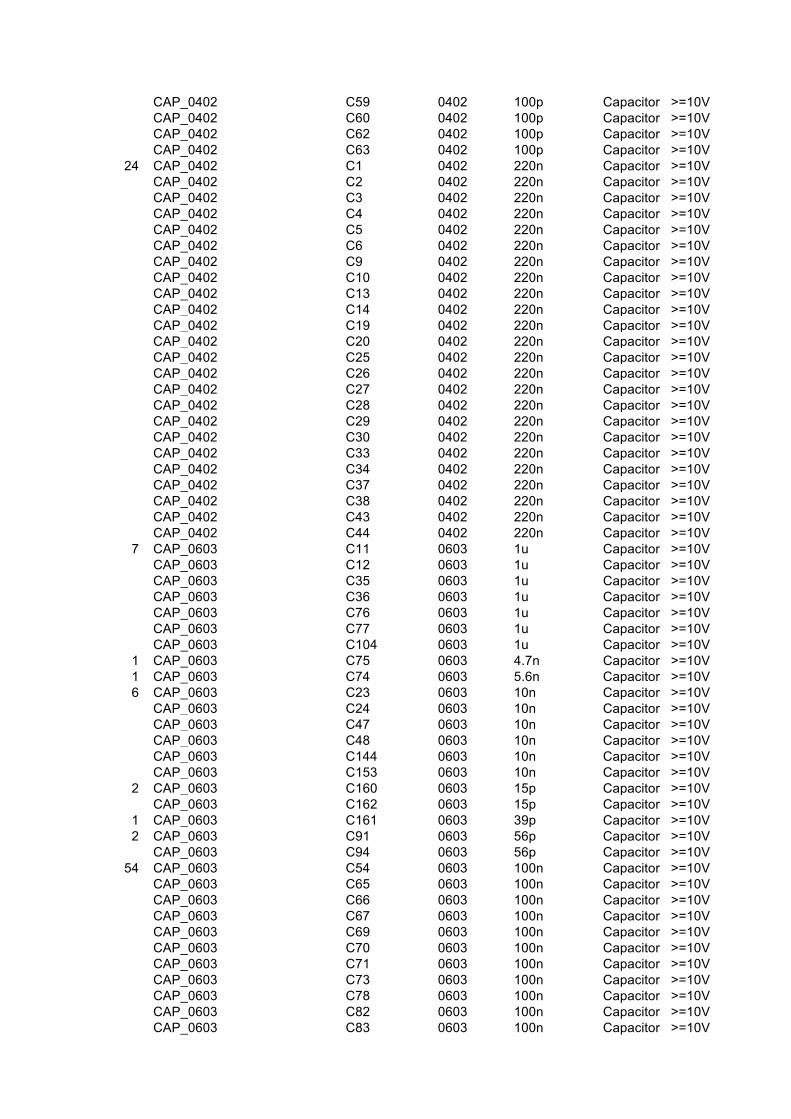
CAP_0402 C59 0402 100p Capacitor >=10V CAP_0402 C60 0402 100p Capacitor >=10V CAP_0402 C62 0402 100p Capacitor >=10V CAP_0402 C63 0402 100p Capacitor >=10V
24 CAP_0402 C1 0402 220n Capacitor >=10V CAP_0402 C2 0402 220n Capacitor >=10V CAP_0402 C3 0402 220n Capacitor >=10V CAP_0402 C4 0402 220n Capacitor >=10V CAP_0402 C5 0402 220n Capacitor >=10V CAP_0402 C6 0402 220n Capacitor >=10V CAP_0402 C9 0402 220n Capacitor >=10V CAP_0402 C10 0402 220n Capacitor >=10V CAP_0402 C13 0402 220n Capacitor >=10V CAP_0402 C14 0402 220n Capacitor >=10V CAP_0402 C19 0402 220n Capacitor >=10V CAP_0402 C20 0402 220n Capacitor >=10V CAP_0402 C25 0402 220n Capacitor >=10V CAP_0402 C26 0402 220n Capacitor >=10V CAP_0402 C27 0402 220n Capacitor >=10V CAP_0402 C28 0402 220n Capacitor >=10V CAP_0402 C29 0402 220n Capacitor >=10V CAP_0402 C30 0402 220n Capacitor >=10V CAP_0402 C33 0402 220n Capacitor >=10V CAP_0402 C34 0402 220n Capacitor >=10V CAP_0402 C37 0402 220n Capacitor >=10V CAP_0402 C38 0402 220n Capacitor >=10V CAP_0402 C43 0402 220n Capacitor >=10V CAP_0402 C44 0402 220n Capacitor >=10V
7 CAP_0603 C11 0603 1u Capacitor >=10V CAP_0603 C12 0603 1u Capacitor >=10V CAP_0603 C35 0603 1u Capacitor >=10V CAP_0603 C36 0603 1u Capacitor >=10V CAP_0603 C76 0603 1u Capacitor >=10V CAP_0603 C77 0603 1u Capacitor >=10V CAP_0603 C104 0603 1u Capacitor >=10V
1 CAP_0603 C75 0603 4.7n Capacitor >=10V 1 CAP_0603 C74 0603 5.6n Capacitor >=10V 6 CAP_0603 C23 0603 10n Capacitor >=10V
CAP_0603 C24 0603 10n Capacitor >=10V CAP_0603 C47 0603 10n Capacitor >=10V CAP_0603 C48 0603 10n Capacitor >=10V CAP_0603 C144 0603 10n Capacitor >=10V CAP_0603 C153 0603 10n Capacitor >=10V
2 CAP_0603 C160 0603 15p Capacitor >=10V CAP_0603 C162 0603 15p Capacitor >=10V
1 CAP_0603 C161 0603 39p Capacitor >=10V 2 CAP_0603 C91 0603 56p Capacitor >=10V
CAP_0603 C94 0603 56p Capacitor >=10V 54 CAP_0603 C54 0603 100n Capacitor >=10V
CAP_0603 C65 0603 100n Capacitor >=10V CAP_0603 C66 0603 100n Capacitor >=10V CAP_0603 C67 0603 100n Capacitor >=10V CAP_0603 C69 0603 100n Capacitor >=10V CAP_0603 C70 0603 100n Capacitor >=10V CAP_0603 C71 0603 100n Capacitor >=10V CAP_0603 C73 0603 100n Capacitor >=10V CAP_0603 C78 0603 100n Capacitor >=10V CAP_0603 C82 0603 100n Capacitor >=10V CAP_0603 C83 0603 100n Capacitor >=10V
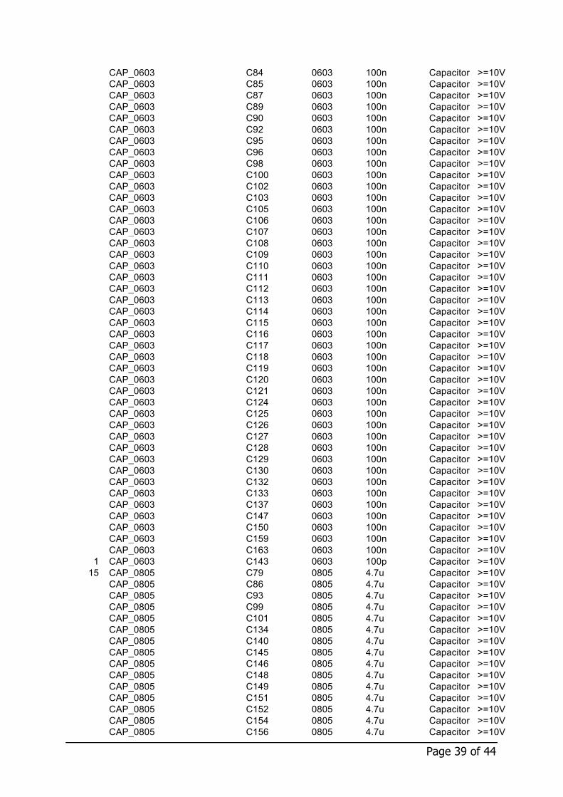
Page 39 of 44
CAP_0603 C84 0603 100n Capacitor >=10V CAP_0603 C85 0603 100n Capacitor >=10V CAP_0603 C87 0603 100n Capacitor >=10V CAP_0603 C89 0603 100n Capacitor >=10V CAP_0603 C90 0603 100n Capacitor >=10V CAP_0603 C92 0603 100n Capacitor >=10V CAP_0603 C95 0603 100n Capacitor >=10V CAP_0603 C96 0603 100n Capacitor >=10V CAP_0603 C98 0603 100n Capacitor >=10V CAP_0603 C100 0603 100n Capacitor >=10V CAP_0603 C102 0603 100n Capacitor >=10V CAP_0603 C103 0603 100n Capacitor >=10V CAP_0603 C105 0603 100n Capacitor >=10V CAP_0603 C106 0603 100n Capacitor >=10V CAP_0603 C107 0603 100n Capacitor >=10V CAP_0603 C108 0603 100n Capacitor >=10V CAP_0603 C109 0603 100n Capacitor >=10V CAP_0603 C110 0603 100n Capacitor >=10V CAP_0603 C111 0603 100n Capacitor >=10V CAP_0603 C112 0603 100n Capacitor >=10V CAP_0603 C113 0603 100n Capacitor >=10V CAP_0603 C114 0603 100n Capacitor >=10V CAP_0603 C115 0603 100n Capacitor >=10V CAP_0603 C116 0603 100n Capacitor >=10V CAP_0603 C117 0603 100n Capacitor >=10V CAP_0603 C118 0603 100n Capacitor >=10V CAP_0603 C119 0603 100n Capacitor >=10V CAP_0603 C120 0603 100n Capacitor >=10V CAP_0603 C121 0603 100n Capacitor >=10V CAP_0603 C124 0603 100n Capacitor >=10V CAP_0603 C125 0603 100n Capacitor >=10V CAP_0603 C126 0603 100n Capacitor >=10V CAP_0603 C127 0603 100n Capacitor >=10V CAP_0603 C128 0603 100n Capacitor >=10V CAP_0603 C129 0603 100n Capacitor >=10V CAP_0603 C130 0603 100n Capacitor >=10V CAP_0603 C132 0603 100n Capacitor >=10V CAP_0603 C133 0603 100n Capacitor >=10V CAP_0603 C137 0603 100n Capacitor >=10V CAP_0603 C147 0603 100n Capacitor >=10V CAP_0603 C150 0603 100n Capacitor >=10V CAP_0603 C159 0603 100n Capacitor >=10V CAP_0603 C163 0603 100n Capacitor >=10V
1 CAP_0603 C143 0603 100p Capacitor >=10V 15 CAP_0805 C79 0805 4.7u Capacitor >=10V
CAP_0805 C86 0805 4.7u Capacitor >=10V CAP_0805 C93 0805 4.7u Capacitor >=10V CAP_0805 C99 0805 4.7u Capacitor >=10V CAP_0805 C101 0805 4.7u Capacitor >=10V CAP_0805 C134 0805 4.7u Capacitor >=10V CAP_0805 C140 0805 4.7u Capacitor >=10V CAP_0805 C145 0805 4.7u Capacitor >=10V CAP_0805 C146 0805 4.7u Capacitor >=10V CAP_0805 C148 0805 4.7u Capacitor >=10V CAP_0805 C149 0805 4.7u Capacitor >=10V CAP_0805 C151 0805 4.7u Capacitor >=10V CAP_0805 C152 0805 4.7u Capacitor >=10V CAP_0805 C154 0805 4.7u Capacitor >=10V CAP_0805 C156 0805 4.7u Capacitor >=10V
16 CAP_1206 C17 1206 10u Capacitor >=10V CAP_1206 C18 1206 10u Capacitor >=10V CAP_1206 C41 1206 10u Capacitor >=10V CAP_1206 C42 1206 10u Capacitor >=10V CAP_1206 C64 1206 10u Capacitor >=10V CAP_1206 C68 1206 10u Capacitor >=10V CAP_1206 C72 1206 10u Capacitor >=10V CAP_1206 C80 1206 10u Capacitor >=10V CAP_1206 C81 1206 10u Capacitor >=10V CAP_1206 C88 1206 10u Capacitor >=10V CAP_1206 C97 1206 10u Capacitor >=10V CAP_1206 C122 1206 10u Capacitor >=10V CAP_1206 C123 1206 10u Capacitor >=10V CAP_1206 C136 1206 10u Capacitor >=10V CAP_1206 C141 1206 10u Capacitor >=10V CAP_1206 C155 1206 10u Capacitor >=10V
1 CAP_1206 C139 1206 22u Capacitor >=10V 1 CAP_1206 C131 1206 100n Capacitor >=10V 1 CAP_1210 C142 1210 47u Capacitor >=10V 2 CAP_1210 C57 1210 100u Capacitor >=10V
CAP_1210 C61 1210 100u Capacitor >=10V 1 CONN_MOLEX_JTAG_FPGA J45 DIL14P_2MM JTAG 1 CY7C68013-56 U37 SSO-G56 Microcontroller 1 DRS4_76 U17 QFN-76 DRS4 2 IND_0603 L14 0603 82nH Inductor
IND_0603 L15 0603 82nH Inductor 8 IND_0603 L1 0603 220nH Inductor
IND_0603 L2 0603 220nH Inductor IND_0603 L3 0603 220nH Inductor IND_0603 L4 0603 220nH Inductor IND_0603 L5 0603 220nH Inductor IND_0603 L6 0603 220nH Inductor IND_0603 L7 0603 220nH Inductor IND_0603 L8 0603 220nH Inductor
1 IND_1008 L11 1008 10uH Inductor 2 IND_1812 L9 1812 10uH Inductor
IND_1812 L10 1812 10uH Inductor 2 JMP2MM JP1 TP50MIL ~WP Jumper
JMP2MM JP2 TP50MIL ~WP Jumper 1 LED_PLCC-4 U39 PLCC-4 blue 1 LED_PLCC-4 U40 PLCC-4 green 1 LED_PLCC-4 U41 PLCC-4 yellow 1 LMZ10503 U43 TO-PMOD-7 TO-PMOD-7 1 LP2985-2.5 U45 SOT23-5 SOT23-5 1 LP2985-3.3 U44 SOT23-5 SOT23-5 1 LTC2600 U23 SSOP16 SSOP16 1 MAX6662 U25 SO-G8 SO-G8 4 MCX-90 J18 MCX-90
MCX-90 J30 MCX-90 MCX-90 J39 MCX-90 MCX-90 J41 MCX-90
4 BAV99s D1 SOT363 switching diodes BAV99s D2 SOT363 switching diodes BAV99s D3 SOT363 switching diodes BAV99s D4 SOT363 switching diodes
1 REG1117-1.2 U47 SOT223 REG 1117A Low Dropout 20 RES_0402 R1 0402 0E Resistor
RES_0402 R3 0402 0E Resistor RES_0402 R37 0402 0E Resistor
Page 41 of 44
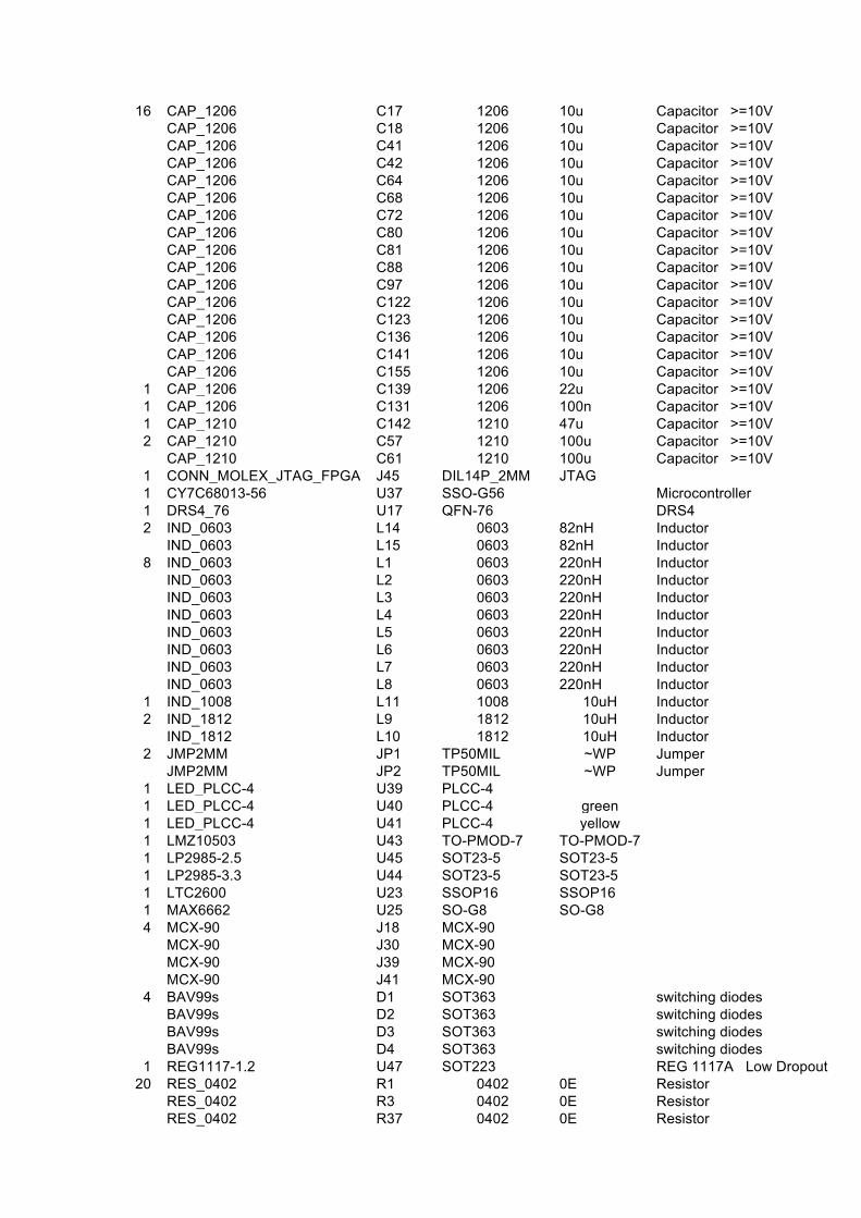
RES_0402 R38 0402 0E Resistor RES_0402 R41 0402 0E Resistor RES_0402 R43 0402 0E Resistor RES_0402 R77 0402 0E Resistor RES_0402 R78 0402 0E Resistor RES_0402 R99 0402 0E Resistor RES_0402 R100 0402 0E Resistor RES_0402 R101 0402 0E Resistor RES_0402 R102 0402 0E Resistor RES_0402 R103 0402 0E Resistor RES_0402 R104 0402 0E Resistor RES_0402 R105 0402 0E Resistor RES_0402 R106 0402 0E Resistor RES_0402 R146 0402 0E Resistor RES_0402 R147 0402 0E Resistor RES_0402 R148 0402 0E Resistor RES_0402 R159 0402 0E Resistor
8 RES_0402 R11 0402 15E Resistor RES_0402 R12 0402 15E Resistor RES_0402 R19 0402 15E Resistor RES_0402 R20 0402 15E Resistor RES_0402 R51 0402 15E Resistor RES_0402 R52 0402 15E Resistor RES_0402 R59 0402 15E Resistor RES_0402 R60 0402 15E Resistor
4 RES_0402 R160 0402 16E Resistor RES_0402 R161 0402 16E Resistor RES_0402 R162 0402 16E Resistor RES_0402 R163 0402 16E Resistor
16 RES_0402 R29 0402 22E Resistor RES_0402 R30 0402 22E Resistor RES_0402 R31 0402 22E Resistor RES_0402 R32 0402 22E Resistor RES_0402 R33 0402 22E Resistor RES_0402 R34 0402 22E Resistor RES_0402 R35 0402 22E Resistor RES_0402 R36 0402 22E Resistor RES_0402 R69 0402 22E Resistor RES_0402 R70 0402 22E Resistor RES_0402 R71 0402 22E Resistor RES_0402 R72 0402 22E Resistor RES_0402 R73 0402 22E Resistor RES_0402 R74 0402 22E Resistor RES_0402 R75 0402 22E Resistor RES_0402 R76 0402 22E Resistor
4 RES_0402 R5 0402 49.9E Resistor RES_0402 R8 0402 49.9E Resistor RES_0402 R45 0402 49.9E Resistor RES_0402 R48 0402 49.9E Resistor
8 RES_0402 R7 0402 61.9E Resistor RES_0402 R10 0402 61.9E Resistor RES_0402 R24 0402 61.9E Resistor RES_0402 R28 0402 61.9E Resistor RES_0402 R47 0402 61.9E Resistor RES_0402 R50 0402 61.9E Resistor RES_0402 R64 0402 61.9E Resistor RES_0402 R68 0402 61.9E Resistor
8 RES_0402 R6 0402 64.9E Resistor RES_0402 R9 0402 64.9E Resistor
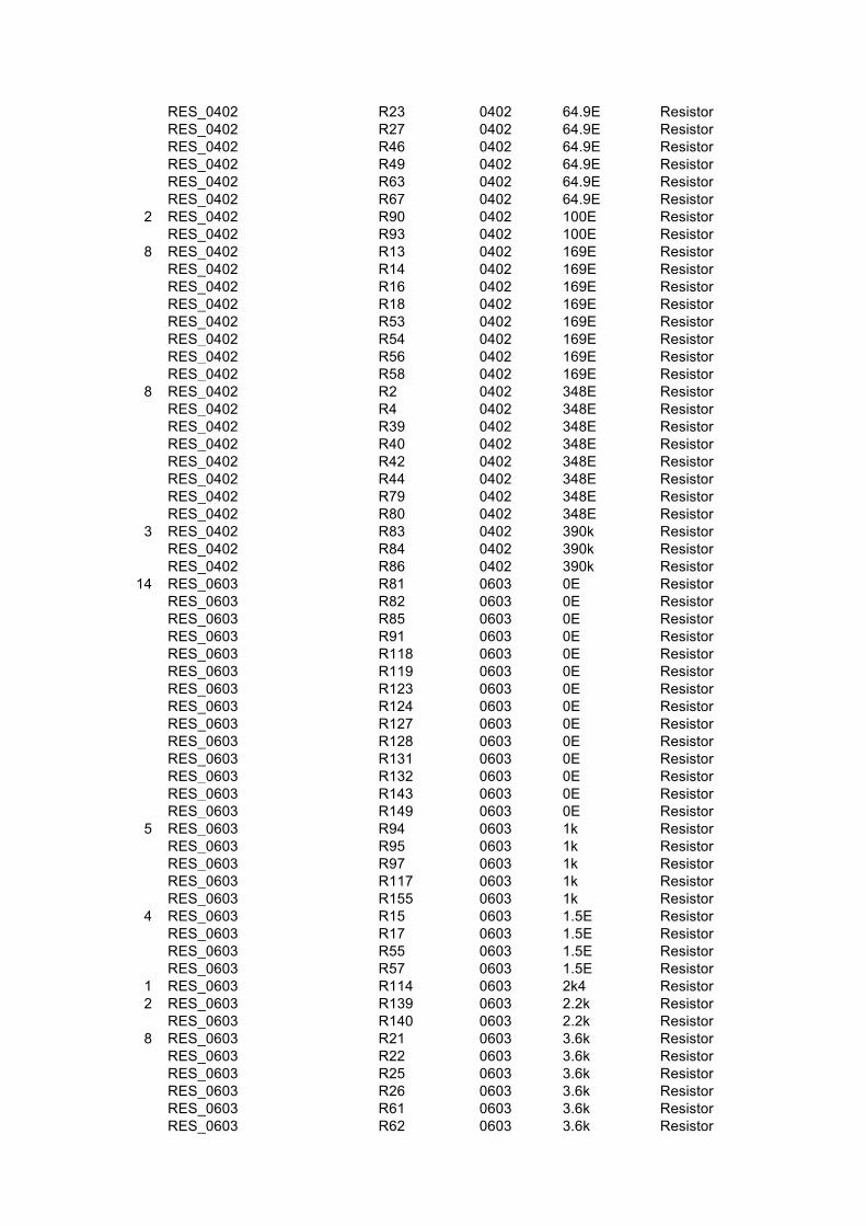
RES_0402 R23 0402 64.9E Resistor RES_0402 R27 0402 64.9E Resistor RES_0402 R46 0402 64.9E Resistor RES_0402 R49 0402 64.9E Resistor RES_0402 R63 0402 64.9E Resistor RES_0402 R67 0402 64.9E Resistor
2 RES_0402 R90 0402 100E Resistor RES_0402 R93 0402 100E Resistor
8 RES_0402 R13 0402 169E Resistor RES_0402 R14 0402 169E Resistor RES_0402 R16 0402 169E Resistor RES_0402 R18 0402 169E Resistor RES_0402 R53 0402 169E Resistor RES_0402 R54 0402 169E Resistor RES_0402 R56 0402 169E Resistor RES_0402 R58 0402 169E Resistor
8 RES_0402 R2 0402 348E Resistor RES_0402 R4 0402 348E Resistor RES_0402 R39 0402 348E Resistor RES_0402 R40 0402 348E Resistor RES_0402 R42 0402 348E Resistor RES_0402 R44 0402 348E Resistor RES_0402 R79 0402 348E Resistor RES_0402 R80 0402 348E Resistor
3 RES_0402 R83 0402 390k Resistor RES_0402 R84 0402 390k Resistor RES_0402 R86 0402 390k Resistor
14 RES_0603 R81 0603 0E Resistor RES_0603 R82 0603 0E Resistor RES_0603 R85 0603 0E Resistor RES_0603 R91 0603 0E Resistor RES_0603 R118 0603 0E Resistor RES_0603 R119 0603 0E Resistor RES_0603 R123 0603 0E Resistor RES_0603 R124 0603 0E Resistor RES_0603 R127 0603 0E Resistor RES_0603 R128 0603 0E Resistor RES_0603 R131 0603 0E Resistor RES_0603 R132 0603 0E Resistor RES_0603 R143 0603 0E Resistor RES_0603 R149 0603 0E Resistor
5 RES_0603 R94 0603 1k Resistor RES_0603 R95 0603 1k Resistor RES_0603 R97 0603 1k Resistor RES_0603 R117 0603 1k Resistor RES_0603 R155 0603 1k Resistor
4 RES_0603 R15 0603 1.5E Resistor RES_0603 R17 0603 1.5E Resistor RES_0603 R55 0603 1.5E Resistor RES_0603 R57 0603 1.5E Resistor
1 RES_0603 R114 0603 2k4 Resistor 2 RES_0603 R139 0603 2.2k Resistor
RES_0603 R140 0603 2.2k Resistor 8 RES_0603 R21 0603 3.6k Resistor
RES_0603 R22 0603 3.6k Resistor RES_0603 R25 0603 3.6k Resistor RES_0603 R26 0603 3.6k Resistor RES_0603 R61 0603 3.6k Resistor RES_0603 R62 0603 3.6k Resistor
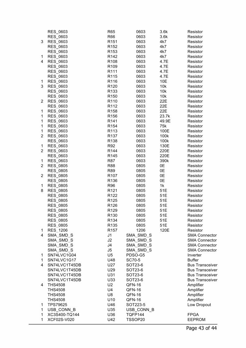
Page 43 of 44
RES_0603 R65 0603 3.6k Resistor RES_0603 R66 0603 3.6k Resistor
3 RES_0603 R151 0603 4k7 Resistor RES_0603 R152 0603 4k7 Resistor RES_0603 R153 0603 4k7 Resistor
1 RES_0603 R142 0603 4k7 Resistor 4 RES_0603 R108 0603 4.7E Resistor
RES_0603 R109 0603 4.7E Resistor RES_0603 R111 0603 4.7E Resistor RES_0603 R115 0603 4.7E Resistor
1 RES_0603 R116 0603 10E Resistor 3 RES_0603 R120 0603 10k Resistor
RES_0603 R133 0603 10k Resistor RES_0603 R150 0603 10k Resistor
2 RES_0603 R110 0603 22E Resistor RES_0603 R112 0603 22E Resistor
1 RES_0603 R158 0603 22E Resistor 1 RES_0603 R156 0603 23.7k Resistor 1 RES_0603 R141 0603 49.9E Resistor 1 RES_0603 R154 0603 75k Resistor 1 RES_0603 R113 0603 100E Resistor 2 RES_0603 R137 0603 100k Resistor
RES_0603 R138 0603 100k Resistor 1 RES_0603 R92 0603 130E Resistor 2 RES_0603 R144 0603 220E Resistor
RES_0603 R145 0603 220E Resistor 1 RES_0603 R87 0603 390k Resistor 2 RES_0805 R88 0805 0E Resistor
RES_0805 R89 0805 0E Resistor 2 RES_0805 R107 0805 0E Resistor
RES_0805 R136 0805 0E Resistor 1 RES_0805 R96 0805 1k Resistor 8 RES_0805 R121 0805 51E Resistor
RES_0805 R122 0805 51E Resistor RES_0805 R125 0805 51E Resistor RES_0805 R126 0805 51E Resistor RES_0805 R129 0805 51E Resistor RES_0805 R130 0805 51E Resistor RES_0805 R134 0805 51E Resistor RES_0805 R135 0805 51E Resistor
1 RES_1206 R157 1206 120E Resistor 4 SMA_SMD_S J1 SMA_SMD_S SMA Connector
SMA_SMD_S J2 SMA_SMD_S SMA Connector SMA_SMD_S J4 SMA_SMD_S SMA Connector SMA_SMD_S J5 SMA_SMD_S SMA Connector
1 SN74LVC1G04 U5 PDSO-G5 Inverter 1 SN74LVC1G17 U48 SC70-5 Buffer 4 SN74LVC1T45DB U27 SOT23-6 Bus Transceiver
SN74LVC1T45DB U29 SOT23-6 Bus Transceiver SN74LVC1T45DB U31 SOT23-6 Bus Transceiver SN74LVC1T45DB U33 SOT23-6 Bus Transceiver
4 THS4508 U2 QFN-16 Amplifier THS4508 U4 QFN-16 Amplifier THS4508 U8 QFN-16 Amplifier THS4508 U10 QFN-16 Amplifier
1 TPS79625 U46 SOT223-5 Low Dropout 1 USB_CONN_B U35 USB_CONN_B 1 XC3S400-TQ144 U36 TQFP144 FPGA 1 XCF02S-V020 U42 TSSOP20 EEPROM