Embed Size (px)
Citation preview
For use in
ECE 212
Electrical Engineering Laboratory II
a companion laboratory for ECE 262, Electric Circuits II
January 2010
Dr. J. E. Harriss
ECE 212
ELECTRICAL ENGINEERING LABORATORY II
ECE 212 ii January 2010
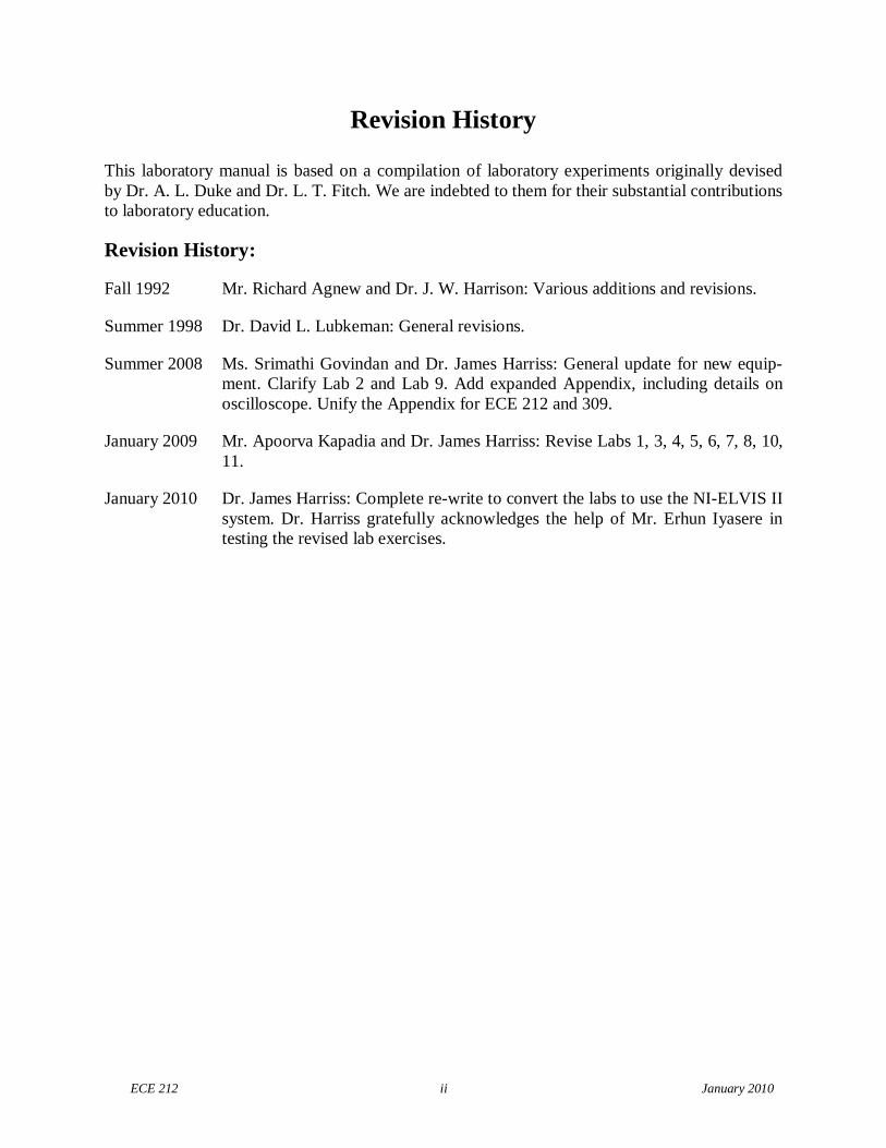
Revision History
This laboratory manual is based on a compilation of laboratory experiments originally devisedby Dr. A. L. Duke and Dr. L. T. Fitch. We are indebted to them for their substantial contributionsto laboratory education.
Revision History:
Fall 1992 Mr. Richard Agnew and Dr. J. W. Harrison: Various additions and revisions.
Summer 1998 Dr. David L. Lubkeman: General revisions.
Summer 2008 Ms. Srimathi Govindan and Dr. James Harriss: General update for new equip-ment. Clarify Lab 2 and Lab 9. Add expanded Appendix, including details onoscilloscope. Unify the Appendix for ECE 212 and 309.
January 2009 Mr. Apoorva Kapadia and Dr. James Harriss: Revise Labs 1, 3, 4, 5, 6, 7, 8, 10,11.
January 2010 Dr. James Harriss: Complete re-write to convert the labs to use the NI-ELVIS IIsystem. Dr. Harriss gratefully acknowledges the help of Mr. Erhun Iyasere intesting the revised lab exercises.
ECE 212 iii January 2010
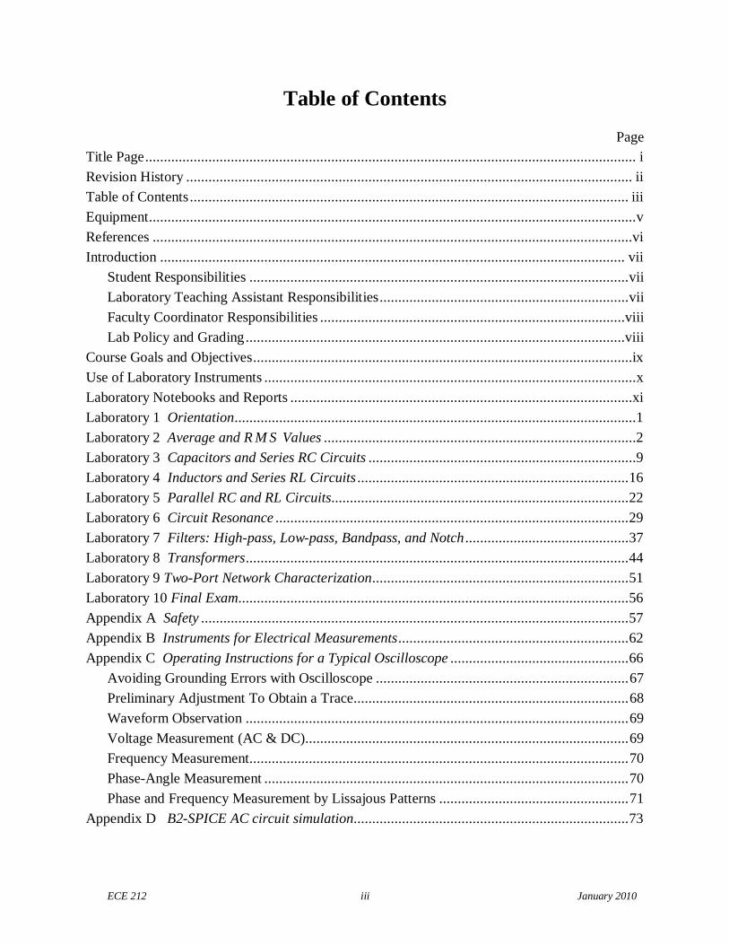
Table of Contents
Page
Title Page.................................................................................................................................... i
Revision History ........................................................................................................................ ii
Table of Contents...................................................................................................................... iii
Equipment...................................................................................................................................v
References .................................................................................................................................vi
Introduction ............................................................................................................................. vii
Student Responsibilities ......................................................................................................vii
Laboratory Teaching Assistant Responsibilities...................................................................vii
Faculty Coordinator Responsibilities ..................................................................................viii
Lab Policy and Grading......................................................................................................viii
Course Goals and Objectives......................................................................................................ix
Use of Laboratory Instruments ....................................................................................................x
Laboratory Notebooks and Reports ............................................................................................xi
Laboratory 1 Orientation............................................................................................................1
Laboratory 2 Average and R M S Values ....................................................................................2
Laboratory 3 Capacitors and Series RC Circuits ........................................................................9
Laboratory 4 Inductors and Series RL Circuits .........................................................................16
Laboratory 5 Parallel RC and RL Circuits................................................................................22
Laboratory 6 Circuit Resonance ...............................................................................................29
Laboratory 7 Filters: High-pass, Low-pass, Bandpass, and Notch ............................................37
Laboratory 8 Transformers.......................................................................................................44
Laboratory 9 Two-Port Network Characterization.....................................................................51
Laboratory 10 Final Exam.........................................................................................................56
Appendix A Safety ...................................................................................................................57
Appendix B Instruments for Electrical Measurements..............................................................62
Appendix C Operating Instructions for a Typical Oscilloscope ................................................66
Avoiding Grounding Errors with Oscilloscope ....................................................................67
Preliminary Adjustment To Obtain a Trace..........................................................................68
Waveform Observation .......................................................................................................69
Voltage Measurement (AC & DC).......................................................................................69
Frequency Measurement......................................................................................................70
Phase-Angle Measurement ..................................................................................................70
Phase and Frequency Measurement by Lissajous Patterns ...................................................71
Appendix D B2-SPICE AC circuit simulation..........................................................................73

ECE 212 iv January 2010
ECE 212 v January 2010
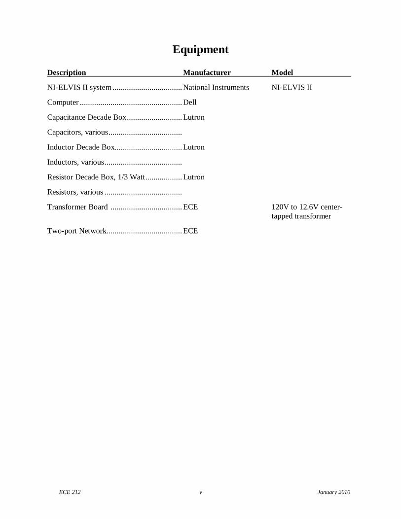
Equipment
Description Manufacturer Model
NI-ELVIS II system.................................. National Instruments NI-ELVIS II
Computer .................................................. Dell
Capacitance Decade Box........................... Lutron
Capacitors, various....................................
Inductor Decade Box................................. Lutron
Inductors, various......................................
Resistor Decade Box, 1/3 Watt.................. Lutron
Resistors, various ......................................
Transformer Board ................................... ECE 120V to 12.6V center-tapped transformer
Two-port Network..................................... ECE
ECE 212 vi January 2010
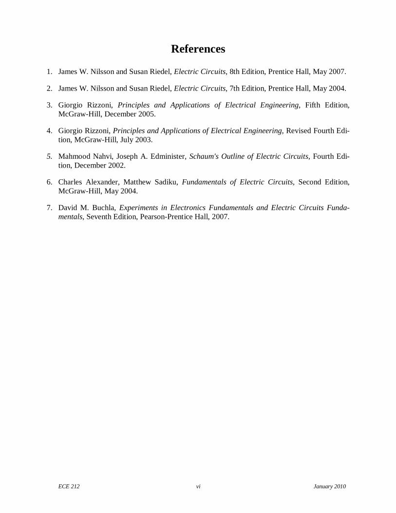
References
1. James W. Nilsson and Susan Riedel, Electric Circuits, 8th Edition, Prentice Hall, May 2007.
2. James W. Nilsson and Susan Riedel, Electric Circuits, 7th Edition, Prentice Hall, May 2004.
3. Giorgio Rizzoni, Principles and Applications of Electrical Engineering, Fifth Edition,McGraw-Hill, December 2005.
4. Giorgio Rizzoni, Principles and Applications of Electrical Engineering, Revised Fourth Edi-tion, McGraw-Hill, July 2003.
5. Mahmood Nahvi, Joseph A. Edminister, Schaum's Outline of Electric Circuits, Fourth Edi-tion, December 2002.
6. Charles Alexander, Matthew Sadiku, Fundamentals of Electric Circuits, Second Edition,McGraw-Hill, May 2004.
7. David M. Buchla, Experiments in Electronics Fundamentals and Electric Circuits Funda-mentals, Seventh Edition, Pearson-Prentice Hall, 2007.
ECE 212 vii January 2010
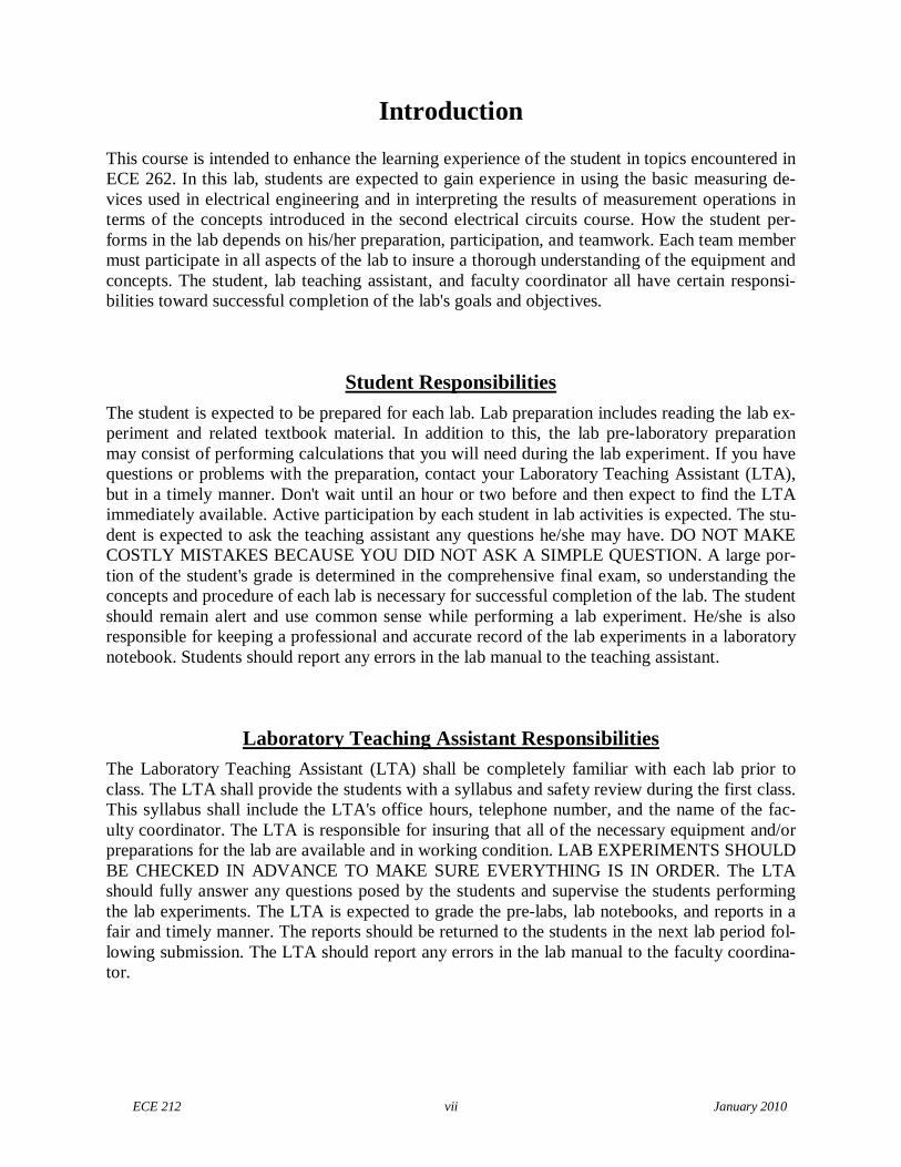
Introduction
This course is intended to enhance the learning experience of the student in topics encountered inECE 262. In this lab, students are expected to gain experience in using the basic measuring de-vices used in electrical engineering and in interpreting the results of measurement operations interms of the concepts introduced in the second electrical circuits course. How the student per-forms in the lab depends on his/her preparation, participation, and teamwork. Each team membermust participate in all aspects of the lab to insure a thorough understanding of the equipment andconcepts. The student, lab teaching assistant, and faculty coordinator all have certain responsi-bilities toward successful completion of the lab's goals and objectives.
Student Responsibilities
The student is expected to be prepared for each lab. Lab preparation includes reading the lab ex-periment and related textbook material. In addition to this, the lab pre-laboratory preparationmay consist of performing calculations that you will need during the lab experiment. If you havequestions or problems with the preparation, contact your Laboratory Teaching Assistant (LTA),but in a timely manner. Don't wait until an hour or two before and then expect to find the LTAimmediately available. Active participation by each student in lab activities is expected. The stu-dent is expected to ask the teaching assistant any questions he/she may have. DO NOT MAKECOSTLY MISTAKES BECAUSE YOU DID NOT ASK A SIMPLE QUESTION. A large por-tion of the student's grade is determined in the comprehensive final exam, so understanding theconcepts and procedure of each lab is necessary for successful completion of the lab. The studentshould remain alert and use common sense while performing a lab experiment. He/she is alsoresponsible for keeping a professional and accurate record of the lab experiments in a laboratorynotebook. Students should report any errors in the lab manual to the teaching assistant.
Laboratory Teaching Assistant Responsibilities
The Laboratory Teaching Assistant (LTA) shall be completely familiar with each lab prior toclass. The LTA shall provide the students with a syllabus and safety review during the first class.This syllabus shall include the LTA's office hours, telephone number, and the name of the fac-ulty coordinator. The LTA is responsible for insuring that all of the necessary equipment and/orpreparations for the lab are available and in working condition. LAB EXPERIMENTS SHOULDBE CHECKED IN ADVANCE TO MAKE SURE EVERYTHING IS IN ORDER. The LTAshould fully answer any questions posed by the students and supervise the students performingthe lab experiments. The LTA is expected to grade the pre-labs, lab notebooks, and reports in afair and timely manner. The reports should be returned to the students in the next lab period fol-lowing submission. The LTA should report any errors in the lab manual to the faculty coordina-tor.
ECE 212 viii January 2010
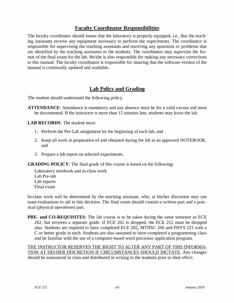
Faculty Coordinator Responsibilities
The faculty coordinator should insure that the laboratory is properly equipped, i.e., that the teach-ing assistants receive any equipment necessary to perform the experiments. The coordinator isresponsible for supervising the teaching assistants and resolving any questions or problems thatare identified by the teaching assistants or the students. The coordinator may supervise the for-mat of the final exam for the lab. He/she is also responsible for making any necessary correctionsto this manual. The faculty coordinator is responsible for insuring that the software version of themanual is continually updated and available.
Lab Policy and Grading
The student should understand the following policy.
ATTENDANCE: Attendance is mandatory and any absence must be for a valid excuse and mustbe documented. If the instructor is more than 15 minutes late, students may leave the lab.
LAB RECORDS: The student must:
1. Perform the Pre-Lab assignment by the beginning of each lab, and
2. Keep all work in preparation of and obtained during the lab in an approved NOTEBOOK,and
3. Prepare a lab report on selected experiments.
GRADING POLICY: The final grade of this course is based on the following:
Laboratory notebook and in-class workLab Pre-labLab reportsFinal exam
In-class work will be determined by the teaching assistant, who, at his/her discretion may useteam evaluations to aid in this decision. The final exam should contain a written part and a prac-tical (physical operations) part.
PRE- and CO-REQUISITES: The lab course is to be taken during the same semester as ECE262, but receives a separate grade. If ECE 262 is dropped, the ECE 212 must be droppedalso. Students are required to have completed ECE 202, MTHSC 206 and PHYS 221 with aC or better grade in each. Students are also assumed to have completed a programming classand be familiar with the use of a computer-based word processor application program.
THE INSTRUCTOR RESERVES THE RIGHT TO ALTER ANY PART OF THIS INFORMA-TION AT HIS/HER DISCRETION IF CIRCUMSTANCES SHOULD DICTATE. Any changesshould be announced in class and distributed in writing to the students prior to their effect.

ECE 212 ix January 2010
Course Goals and Objectives
The Electrical Circuits Laboratory II is designed to provide the student with the knowledge touse basic measuring instruments and techniques with proficiency. These techniques are designedto complement the concepts introduced in ECE 262. In addition, the student should learn how toeffectively record experimental results and present these results in a written report. More explic-itly, the class objectives are:
1. To gain proficiency in the use of common measuring instruments;
2. To enhance understanding of advanced electric circuit analysis concepts.
Inductance, Capacitance, and reactance
AC voltage and current addition. Phasors
AC power (real and reactive, instantaneous and average)
Series and parallel resonant circuit behavior
Passive Filters
Transfer functions
Transformers
Two-port network analysis;
3. To develop communication skills through
a) maintenance of succinct but complete laboratory notebooks as permanent, writtendescriptions of procedures, results, and analyses,
b) verbal interchanges with the Laboratory Instructor and other students, and
c) preparation of succinct but complete laboratory reports;
4. To compare theoretical predictions with experimental results and to resolve any ap-parent differences.
ECE 212 x January 2010
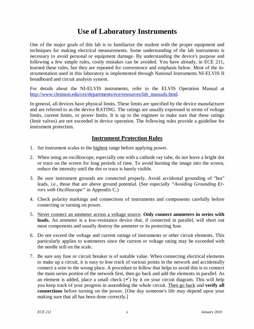
Use of Laboratory Instruments
One of the major goals of this lab is to familiarize the student with the proper equipment andtechniques for making electrical measurements. Some understanding of the lab instruments isnecessary to avoid personal or equipment damage. By understanding the device's purpose andfollowing a few simple rules, costly mistakes can be avoided. You have already, in ECE 211,learned these rules, but they are repeated for convenience and emphasis below. Most of the in-strumentation used in this laboratory is implemented through National Instruments NI-ELVIS IIbreadboard and circuit analysis system.
For details about the NI-ELVIS instruments, refer to the ELVIS Operation Manual athttp://www.clemson.edu/ces/departments/ece/resources/lab_manuals.html.
In general, all devices have physical limits. These limits are specified by the device manufacturerand are referred to as the device RATING. The ratings are usually expressed in terms of voltagelimits, current limits, or power limits. It is up to the engineer to make sure that these ratings(limit valves) are not exceeded in device operation. The following rules provide a guideline forinstrument protection.
Instrument Protection Rules
1. Set instrument scales to the highest range before applying power.
2. When using an oscilloscope, especially one with a cathode ray tube, do not leave a bright dotor trace on the screen for long periods of time. To avoid burning the image into the screen,reduce the intensity until the dot or trace is barely visible.
3. Be sure instrument grounds are connected properly. Avoid accidental grounding of "hot"leads, i.e., those that are above ground potential. (See especially “Avoiding Grounding Er-rors with Oscilloscope” in Appendix C.)
4. Check polarity markings and connections of instruments and components carefully beforeconnecting or turning on power.
5. Never connect an ammeter across a voltage source. Only connect ammeters in series withloads. An ammeter is a low-resistance device that, if connected in parallel, will short outmost components and usually destroy the ammeter or its protecting fuse.
6. Do not exceed the voltage and current ratings of instruments or other circuit elements. Thisparticularly applies to wattmeters since the current or voltage rating may be exceeded withthe needle still on the scale.
7. Be sure any fuse or circuit breaker is of suitable value. When connecting electrical elementsto make up a circuit, it is easy to lose track of various points in the network and accidentallyconnect a wire to the wrong place. A procedure to follow that helps to avoid this is to connectthe main series portion of the network first, then go back and add the elements in parallel. Asan element is added, place a small check () by it on your circuit diagram. This will helpyou keep track of your progress in assembling the whole circuit. Then go back and verify allconnections before turning on the power. [One day someone's life may depend upon yourmaking sure that all has been done correctly.]
ECE 212 xi January 2010
Laboratory Notebooks and Reports
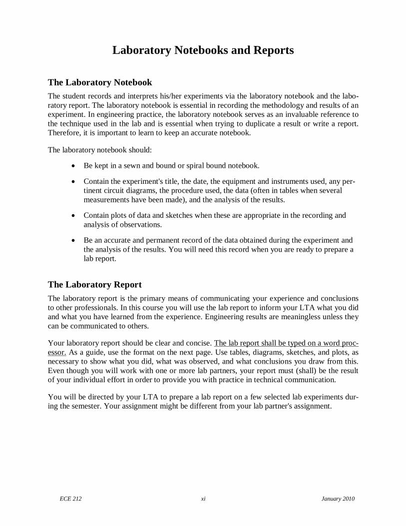
The Laboratory Notebook
The student records and interprets his/her experiments via the laboratory notebook and the labo-ratory report. The laboratory notebook is essential in recording the methodology and results of anexperiment. In engineering practice, the laboratory notebook serves as an invaluable reference tothe technique used in the lab and is essential when trying to duplicate a result or write a report.Therefore, it is important to learn to keep an accurate notebook.
The laboratory notebook should:
Be kept in a sewn and bound or spiral bound notebook.
Contain the experiment's title, the date, the equipment and instruments used, any per-tinent circuit diagrams, the procedure used, the data (often in tables when severalmeasurements have been made), and the analysis of the results.
Contain plots of data and sketches when these are appropriate in the recording andanalysis of observations.
Be an accurate and permanent record of the data obtained during the experiment andthe analysis of the results. You will need this record when you are ready to prepare alab report.
The Laboratory Report
The laboratory report is the primary means of communicating your experience and conclusionsto other professionals. In this course you will use the lab report to inform your LTA what you didand what you have learned from the experience. Engineering results are meaningless unless theycan be communicated to others.
Your laboratory report should be clear and concise. The lab report shall be typed on a word proc-essor. As a guide, use the format on the next page. Use tables, diagrams, sketches, and plots, asnecessary to show what you did, what was observed, and what conclusions you draw from this.Even though you will work with one or more lab partners, your report must (shall) be the resultof your individual effort in order to provide you with practice in technical communication.
You will be directed by your LTA to prepare a lab report on a few selected lab experiments dur-ing the semester. Your assignment might be different from your lab partner's assignment.
ECE 212 xii January 2010
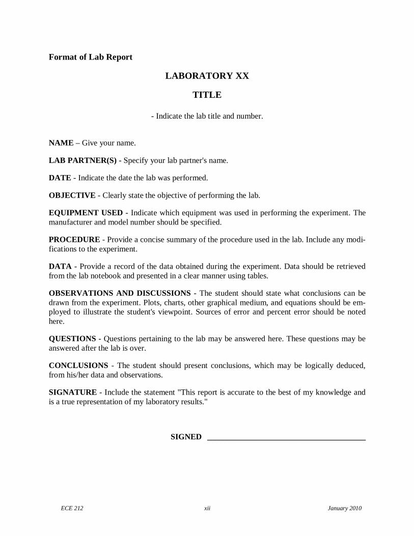
Format of Lab Report
LABORATORY XX
TITLE
- Indicate the lab title and number.
NAME – Give your name.
LAB PARTNER(S) - Specify your lab partner's name.
DATE - Indicate the date the lab was performed.
OBJECTIVE - Clearly state the objective of performing the lab.
EQUIPMENT USED - Indicate which equipment was used in performing the experiment. Themanufacturer and model number should be specified.
PROCEDURE - Provide a concise summary of the procedure used in the lab. Include any modi-fications to the experiment.
DATA - Provide a record of the data obtained during the experiment. Data should be retrievedfrom the lab notebook and presented in a clear manner using tables.
OBSERVATIONS AND DISCUSSIONS - The student should state what conclusions can bedrawn from the experiment. Plots, charts, other graphical medium, and equations should be em-ployed to illustrate the student's viewpoint. Sources of error and percent error should be notedhere.
QUESTIONS - Questions pertaining to the lab may be answered here. These questions may beanswered after the lab is over.
CONCLUSIONS - The student should present conclusions, which may be logically deduced,from his/her data and observations.
SIGNATURE - Include the statement "This report is accurate to the best of my knowledge andis a true representation of my laboratory results."
SIGNED _______________________________________
ECE 212 1 January 2010
Laboratory 1
Orientation
INTRODUCTION: In the first lab period, the students should become familiar with the locationof equipment and components in the lab, the course requirements, and the teaching instructor.Students should also make sure that they have all of the co- and pre-requisites for the course atthis time.
OBJECTIVE: To familiarize the students with the lab facilities, equipment, standard operatingprocedures, lab safety, and the course requirements.
PRE-LAB: Read the introduction and Appendix A (Safety) of this manual.
EQUIPMENT NEEDED: Lab Manual.
PROCEDURE: During the first laboratory period, the instructor will provide the students with ageneral idea of what is expected from them in this course. Each student will receive a copy of thesyllabus, stating the instructor's office hours and contact information. In addition, the instructorwill review the safety concepts of the course. The instructor will indicate which word processorshould be used for the lab reports. The students should familiarize themselves with the preferredword processor software.
During this period the Instructor will briefly review the measuring instruments and other equip-ment that will be used. The location of instruments, equipment, and components (e.g. resistors,capacitors, connecting wiring) will be indicated. The guidelines for instrument use will be re-viewed. Most of the instrumentation used in this laboratory is implemented through National In-struments NI-ELVIS II breadboard and circuit analysis system.
You should record in your notebook the information from your LTA.
REPORT: No report is due next time.
ECE 212 2 January 2010
Laboratory 2
Average and RMS Values
INTRODUCTION: Waveforms of voltage and current that vary periodically with time may becharacterized by their average value or their root mean square (r m s) value. The latter is usedto determine the power supplied, dissipated, or stored by a circuit element. Some of themeasuring instruments you will use respond to average values of voltage or current, whileothers respond to r m s values.
EDUCATIONAL OBJECTIVE:
(1) Learn how to determine the values of r m s voltage for three types of waveforms: a sinu-soid, a square wave, and a triangular wave.
(2) Understand the difference between a true-r ms and a conventional multimeter.
EXPERIMENTAL OBJECTIVE:
Determine whether the voltage metering function of the NI-ELVIS’s Digital Multimeter(DMM) measures true RMS voltage for three types of waveforms: a sinusoid, a square wave,and a triangular wave.
PRE-LAB:
Reading:
Read Appendix B and Appendix C of this manual, paying particular attention to themethods of using measurement instruments.
Written:
(a) Using the definition of average value (equation 2.1) and r m s value (equation 2.2), calcu-late the average voltage, the average absolute voltage, and the r m s voltage values for thesymmetrical sine, square, and triangular waveforms, assuming that the peak value of eachwaveform is 2 V.
(b) Compute the voltage values that would be reported by non-true r m s voltmeters. Youmay use the equations derived in the Background section for these calculations. Show allof your calculations in your lab notebook and summarize the results in a table.
(c) After you have done these calculations, review the laboratory exercise procedures andplan how you will use the experience gained in these calculations to find the valuessought.
EQUIPMENT NEEDED:
NI-ELVIS II, including
Function Generator
Digital Multimeter (DMM)
Oscilloscope
Resistance Decade Box
ECE 212 3 January 2010
BACKGROUND
Measurements of AC signal:
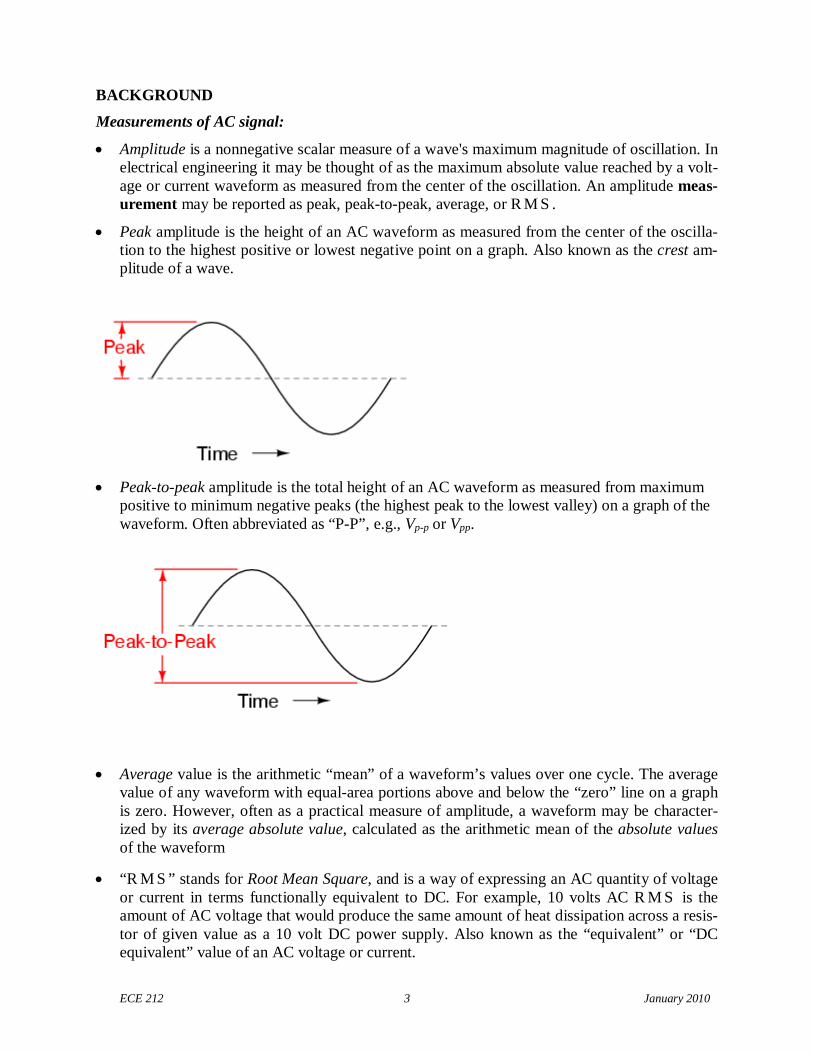
Amplitude is a nonnegative scalar measure of a wave's maximum magnitude of oscillation. Inelectrical engineering it may be thought of as the maximum absolute value reached by a volt-age or current waveform as measured from the center of the oscillation. An amplitude meas-urement may be reported as peak, peak-to-peak, average, or R M S .
Peak amplitude is the height of an AC waveform as measured from the center of the oscilla-tion to the highest positive or lowest negative point on a graph. Also known as the crest am-plitude of a wave.
Peak-to-peak amplitude is the total height of an AC waveform as measured from maximumpositive to minimum negative peaks (the highest peak to the lowest valley) on a graph of thewaveform. Often abbreviated as “P-P”, e.g., Vp-p or Vpp.
Average value is the arithmetic “mean” of a waveform’s values over one cycle. The averagevalue of any waveform with equal-area portions above and below the “zero” line on a graphis zero. However, often as a practical measure of amplitude, a waveform may be character-ized by its average absolute value, calculated as the arithmetic mean of the absolute valuesof the waveform
“R M S ” stands for Root Mean Square, and is a way of expressing an AC quantity of voltageor current in terms functionally equivalent to DC. For example, 10 volts AC R M S is theamount of AC voltage that would produce the same amount of heat dissipation across a resis-tor of given value as a 10 volt DC power supply. Also known as the “equivalent” or “DCequivalent” value of an AC voltage or current.
ECE 212 4 January 2010
Analog, electromechanical meter movements respond proportionally to the average absolutevalue of an AC voltage or current. When R M S indication is desired, the meter's calibrationmust be adjusted accordingly, usually by applying a constant multiplicative factor assumedfor a sinusoidal wave. This means that the accuracy of an electromechanical meter's RMSindication is dependent on the purity of the waveform and whether it is the same wave shapeas the waveform used in calibrating.
In this experiment, we will work with periodic waveforms having period T and amplitude Vm.Specifically, we will work with the following three types of waveforms:
1. A sinusoidal wave voltage: v(t) = Vm cos(2πt/T) .
2. A square-wave voltage:
3( ) 0 ; ;
2 2
3( ) ; 2 ;
2 2
m
m
T Tv t V for t T t etc
T Tv t V for t T t T etc
3. A triangular-wave voltage:
( ) 4 [( ) / ] ¼ ¼
( ) ¼ ¼ ¾
0,1,2,3,
m
m
v t V t nT T for n T t n T
v t V t n T T for n T t n T
where n
AC voltage and current waveforms are further depicted in a number of ways. Two of the mostcommon and useful are the average and the root-mean-square (r m s ) values.
The average value of a time-varying waveform x(t) with period T is given by:
0
1( )
T
aveX x t dtT
(2.1)
The root-mean-square value, useful for power calculations, is defined by:
2
0
1( )
T
rmsX x t dtT
(2.2)
Since the sine, square, and triangular waveforms are symmetrical about the time axis, they allhave mathematical average voltages of zero. However, each waveform will have an r m s value,and a summary of the calculation steps for relating the voltage magnitude to the r m s value foreach waveform is shown below:
ECE 212 5 January 2010
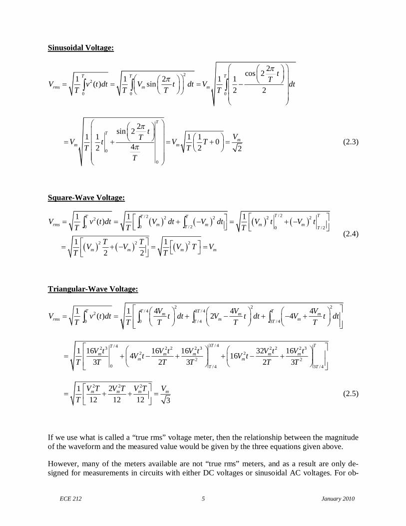
Sinusoidal Voltage:
2
2
0 0 0
2cos 2
1 1 2 1 1( ) sin
2 2
T T T
rms m m
tT
V v t dt V t dt V dtT T T T
0
0
2sin 2
1 1 1 10
42 2 2
T
T
mm m
tVT
V t V TT T
T
(2.3)
Square-Wave Voltage:
/ 2/ 2 2 2 2 22
0 0 / 2 0 / 2
2 2 2
1 1 1( )
1 1
2 2
T TT T T
rms m m m mT T
m m m m
V v t dt V dt V dt V t V tT T T
T TV V V T V
T T
(2.4)
Triangular-Wave Voltage:
2 2 2/ 4 3 / 4
2
0 0 / 4 3 / 4
4 4 41 1( ) 2 4
T T T Tm m m
rms m mT T
V V VV v t dt t dt V t dt V t dt
T T T T T
3 / 4/ 42 3 2 2 2 3 2 2 2 32 2
2 2
0 / 4 3 / 4
16 16 16 32 1614 16
3 2 3 2 3
T TT
m m m m mm m
T T
V t V t V t V t V tV t V t
T T T T T T
2 2 221
12 12 12 3m m m mV T V T V T V
T
(2.5)
If we use what is called a “true rms” voltage meter, then the relationship between the magnitudeof the waveform and the measured value would be given by the three equations given above.
However, many of the meters available are not “true rms” meters, and as a result are only de-signed for measurements in circuits with either DC voltages or sinusoidal AC voltages. For ob-
ECE 212 6 January 2010
taining the AC voltage, most digital meters effectively perform a full-wave rectification of thewaveform and compute the average absolute value. A constant factor is then applied to computean RMS value. Often the constant factor is chosen to give a correct result for a sinusoidal wave-form.
For a sinusoidal waveform, the average value for the rectified voltage is calculated as follows:
/ 2
0 0 0 / 2
1 1 2 2 2( ) sin sin sin
T T T Tm
ave rect m m mT
VV v t dt V t dt V t dt V t dt
T T T T T T
/ 2/ 2
00
2 2 22 2sin cos
2
TT
m m mm
V V VTV t dt t
T T T T
(2.6)
Since the rms value for a sinusoidal waveform should be related to the amplitude by 2 , weneed to apply a conversion factor to get the correct rms value on the meter readout. In this casethe conversion factor would be:
11.111*
22rms avg rectified avg rectifiedV V V
(2.7)
Now what happens when we measure a square wave with 50% duty cycle? To find out, we com-pute the average of the rectified square-wave waveform:
/ 2
0 0 / 2
1 1( )
T T T
avg rectified m m mTV v t dt V dt V dt V
T T (2.8)
The non-true-rms meter will apply the same conversion factor it applied to the sine wave. Hence,what we will see on the meter readout for a square wave is:
1.111*meter mV V (2.9)
This meter will report a rms value that is 11% higher than the actual rms value we should havefor a square wave.
Finally, for a triangular waveform, the average rectified voltage is:
/ 4 / 2 3 / 4
0 0 / 4 / 2 3 / 4
4 4 4 41 1( ) 2 2 4
T T T T Tm m m m
avg rectified m m mT T T
V V V VV v t dt t dt V t dt V t dt V t dt
T T T T T T
/ 4 / 2 3 / 42 2 2 2
0 / 4 / 2 3 / 4
4 4 4 412 2 4
2 2 2 2 2
T T T T
m m m m m
m m m
T T T
V t V t V t V t VV t V t V t
T T T T T
(2.10)
So for a triangular waveform the rms voltage indicated on the non-true-rms meter will be
ECE 212 7 January 2010
1.111* 0.555*2m
meter m
VV V (2.11)
while it should be registering 3mV = 0.577*Vm. This meter gives a reading only 96% of what
we should actually get, and so will under-report the rms voltage for a triangular wave.
In practice you will not get the exact results predicted by the equations, due to a number of er-rors, such as inability to set the peak voltage to the exact value, slight errors in the meter reading,and inaccuracies in the shape of the waveform produced by the function generator. Also, wehave assumed that the duty cycle of the square wave is exactly 50% in these calculations, whichmight not actually be the case for your waveform generator.
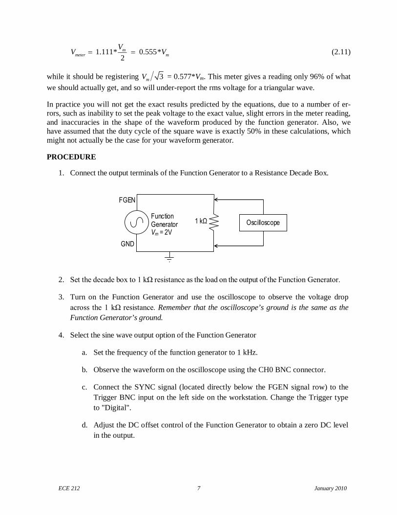
PROCEDURE
1. Connect the output terminals of the Function Generator to a Resistance Decade Box.
2. Set the decade box to 1 kΩ resistance as the load on the output of the Function Generator.
3. Turn on the Function Generator and use the oscilloscope to observe the voltage drop
across the 1 kΩ resistance. Remember that the oscilloscope’s ground is the same as the
Function Generator’s ground.
4. Select the sine wave output option of the Function Generator
a. Set the frequency of the function generator to 1 kHz.
b. Observe the waveform on the oscilloscope using the CH0 BNC connector.
c. Connect the SYNC signal (located directly below the FGEN signal row) to the
Trigger BNC input on the left side on the workstation. Change the Trigger type
to "Digital".
d. Adjust the DC offset control of the Function Generator to obtain a zero DC level
in the output.
Oscilloscope1 kΩFunctionGeneratorVm = 2V
FGEN
GND
ECE 212 8 January 2010
e. Use the Function Generator’s output level control (Amplitude control
knob/numerical input) to obtain a 2.0 Volt peak value (4.0 Vpp) on the scope
measurement.
f. Use the digital multimeter (DMM) AC Voltage [V~] function to measure the
Function Generator [FGEN] voltage by connecting the VΩ and COM banana
jacks to FGEN and GND respectively. Make sure to include DC offset values in
the RMS calculation.
5. Repeat the steps from 4a to 4f using a triangular wave output from the Function Generator.
6. Repeat the steps from 4a to 4f using a square wave (50% duty factor) output from the Func-
tion Generator.
7. Adjust the DC offset control to add a 2 Volt DC offset to the original 1 kHz sine wave.
Now the waveform should vary from 0 to 4 Volts. Sketch this waveform in your lab
notebook. Use the DMM to measure the AC RMS voltage and the DC voltage across the
resistance. Record the values. Repeat this same step for triangular wave and square wave.
PROBING FURTHER
1. Compare the RMS voltage value calculations you made for the Pre-Lab to the AC voltagemeasurements made in 4th, 5th, and 6th steps in the Procedure. Do your measured valuesagree with the calculated values in all cases? If not, why?
2. Determine the theoretical RMS voltage value and DC voltage value you should havemeasured in Step 7 of the Procedure and compare this to what you actually measured.Show all of your math calculations. Do your measured values agree with the calculatedvalues? If not, why?
3. Summarize your comparisons: Does the digital multimeter (DMM) in the NI-ELVIS pro-vide true RMS measurements of voltage for all three waveforms? Justify your conclusion.
REPORT: Your Laboratory Teaching Assistant will inform you when a report is due, and onwhich experiments you will report. Make sure that you have recorded all necessary informationand data in your laboratory notebook to enable you to prepare a report on this experiment, if sodirected, at some time in the future.
ECE 212 9 January 2010
Laboratory 3
Capacitors and Series RC Circuits
INTRODUCTION: Linear circuit elements — resistors, capacitors, and inductors — are thebackbone of electrical and electronic circuits. These three types of elements respond to elec-trical voltages in different ways, variously consuming, storing, or supplying electrical energy.Understanding these behaviors and learning to calculate the result of combining elements iscritical for designing and working with electric circuits. While a resistor consumes electricalenergy, converting it to heat, capacitors and inductors vary their responses according to thefrequency of the voltage or current applied to them. This laboratory will explore those re-sponses for series-connected capacitors.
EDUCATIONAL OBJECTIVES:(1) Learn to avoid oscilloscope grounding errors when measuring voltages. Learn the two-channel
difference method and the interchanging-components method (Appendix C).(2) Learn to measure capacitive reactance.(3) Learn to measure phase angles between voltages.(4) Learn to draw impedance and voltage phasor diagrams for resistors and capacitors in series.(5) Understand how impedance and voltage phasors add (i.e., like vectors).(6) Learn to simulate AC series circuit in B2-SPICE.
EXPERIMENTAL OBJECTIVES:(1) Confirm how capacitances add when two capacitors are connected in parallel; in series.(2) Determine the reactance of a capacitor in a series RC circuit by measuring voltages.(3) Draw impedance and voltage phasor diagrams for a series RC circuit.(4) Explain the effect of frequency on the impedance and voltage phasors for a series RC circuit.
PRE-LAB:
Reading: (1) Read and study the Background section of this Laboratory. (2) Read AppendixC, especially Avoiding Grounding Errors with Oscilloscope, Voltage Measurement, andPhase-Angle Measurement for an oscilloscope with two vertical inputs.
Written: (1) In your lab notebook sketch the circuit diagram to be used in the procedure andprepare Tables 3.1 and 3.2 to record data. (2) Sketch the impedance and voltage phasorsdiagrams (as in Figure 3.2) you would get at 500 Hz for the circuit in Figure 3.3. (3)Make a table of the magnitudes and phase angles. You will use this to check that yourexperimental setup is correct.
EQUIPMENT NEEDED:
NI-ELVIS II
Function generator
Oscilloscope
Digital Multimeter
Resistor decade box
Capacitors, 0.01 µf, qty 2 (discrete capacitors)
ECE 212 10 January 2010
BACKGROUND
A capacitor is formed whenever two conductors are separated by an insulating material. Considerthe simple example of two parallel conducting plates separated by a small gap that is filled withan insulating material (vacuum, air, glass, or other dielectric). If a potential difference exists be-tween the two plates, then an electric field exists between them, and opposite electric chargeswill be attracted to the two plates. The ability to store that electric charge is a fundamental prop-erty of capacitors. The larger the plates, the more charge can be stored. The closer the plates, themore charge can be stored…at least until the charges leap the gap and the dielectric breaks down.
If a voltage source is connected across a capacitor, charge will flow in the external circuit untilthe voltage across the capacitor is equal to the applied voltage. The charge that flows is propor-tional to the size of the capacitor (its “capacitance”) and to the applied voltage. The relationshipis given by the equation
Q = CV
where Q is the charge in coulombs, C is the capacitance in farads, and V is the applied voltage involts.
Capacitors in SeriesElectric current I is the amount of charge that flows per unit time; that is, I = Q/T. Thus, the totalcharge that flows through a circuit (or a capacitor) is Q = IT. So, if two capacitors are connectedin series and a voltage is applied across the pair, the same current, and therefore the same charge,must flow through both capacitors, and the total voltage VT must be divided across both capaci-tors:
1 2
1 2 1 2
1 1T
T
Q Q QV V V Q
C C C C C
where V1 and V2 are the voltages across the capacitors with capacitances C1 and C2. Thus, CT,the total capacitance of two capacitors in series, is found by
1 2
1 2 1 2
1 1 1T
T
C Cor C
C C C C C
.
Capacitors in ParallelConnecting capacitors in parallel is effectively the same as making a single capacitor’s plateslarger, and therefore able to hold more charge for a given applied voltage. This simple view isborne out if one analyzes the flow of charge through a parallel array of capacitors connected to avoltage source. The result of such analysis is that capacitances in parallel add directly:
CT = C1 + C2 + C3 +….
ECE 212 11 January 2010
Time ConstantIf a voltage V0 is applied to a capacitor C connected in series with a resistor R, the voltage acrossthe capacitor gradually increases. The rate at which the capacitor’s voltage changes is character-ized by a “time constant”, τ:
τ = RC
τ is the time required for the voltage on the capacitor to rise from 0 to 0.632 V0.
τ is also the time required for the voltage of a fully charged capacitor to fall from V0 to 0.368 V0.The number 0.368 = e–1 and the number 0.632 = (1– e–1 ).
Capacitive ReactanceReactance is a characteristic exhibited by capacitors and inductors in circuits with time-varyingvoltages and currents, such as common sinusoidal AC circuits. Like resistance, reactance op-poses the flow of electric current and is measured in ohms. Capacitive reactance XC can be foundby the equation:
1
2CX
f C
where f is the frequency of the applied voltage or current and C is the capacitance in farads. Aswith resistance, reactance obeys Ohm’s law:
CC C C C
C
VV I X or X
I
If a sinusoidal voltage is applied across a resistor, the current through the resistor is in phasewith the voltage. That is not true for a capacitor. If we connect a capacitor across a sinusoidalvoltage, the maximum current flows through the capacitor when the voltage’s rate of change ismaximum (i.e., at V=0), and diminishes as the voltage on the capacitor increases, until finally thecurrent is zero when the voltage is at maximum and its derivative is zero. At that instant, themaximum possible charge for the applied voltage is stored in the capacitor, and so the flow ofcharge (i.e., the current) stops.
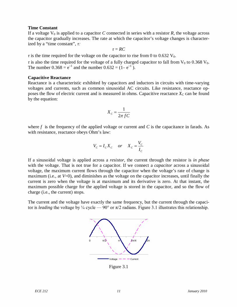
The current and the voltage have exactly the same frequency, but the current through the capaci-tor is leading the voltage by ¼ cycle — 90° or π/2 radians. Figure 3.1 illustrates this relationship.
0 π/2 π 3π/4 2π
Voltage Current
Figure 3.1
ECE 212 12 January 2010
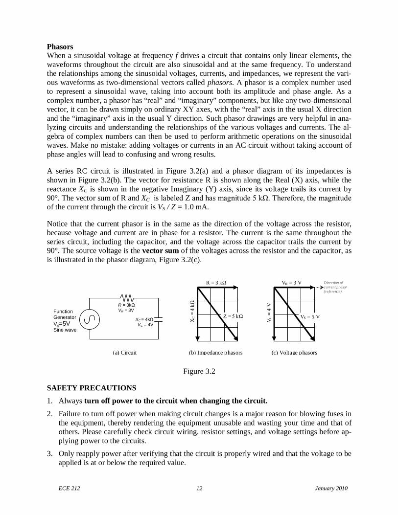
PhasorsWhen a sinusoidal voltage at frequency f drives a circuit that contains only linear elements, thewaveforms throughout the circuit are also sinusoidal and at the same frequency. To understandthe relationships among the sinusoidal voltages, currents, and impedances, we represent the vari-ous waveforms as two-dimensional vectors called phasors. A phasor is a complex number usedto represent a sinusoidal wave, taking into account both its amplitude and phase angle. As acomplex number, a phasor has “real” and “imaginary” components, but like any two-dimensionalvector, it can be drawn simply on ordinary XY axes, with the “real” axis in the usual X directionand the “imaginary” axis in the usual Y direction. Such phasor drawings are very helpful in ana-lyzing circuits and understanding the relationships of the various voltages and currents. The al-gebra of complex numbers can then be used to perform arithmetic operations on the sinusoidalwaves. Make no mistake: adding voltages or currents in an AC circuit without taking account ofphase angles will lead to confusing and wrong results.
A series RC circuit is illustrated in Figure 3.2(a) and a phasor diagram of its impedances isshown in Figure 3.2(b). The vector for resistance R is shown along the Real (X) axis, while thereactance XC is shown in the negative Imaginary (Y) axis, since its voltage trails its current by90°. The vector sum of R and XC is labeled Z and has magnitude 5 kΩ. Therefore, the magnitude of the current through the circuit is VS / Z = 1.0 mA.
Notice that the current phasor is in the same as the direction of the voltage across the resistor,because voltage and current are in phase for a resistor. The current is the same throughout theseries circuit, including the capacitor, and the voltage across the capacitor trails the current by90°. The source voltage is the vector sum of the voltages across the resistor and the capacitor, asis illustrated in the phasor diagram, Figure 3.2(c).
Figure 3.2
SAFETY PRECAUTIONS
1. Always turn off power to the circuit when changing the circuit.
2. Failure to turn off power when making circuit changes is a major reason for blowing fuses inthe equipment, thereby rendering the equipment unusable and wasting your time and that ofothers. Please carefully check circuit wiring, resistor settings, and voltage settings before ap-plying power to the circuits.
3. Only reapply power after verifying that the circuit is properly wired and that the voltage to beapplied is at or below the required value.
R = 3kΩ VR = 3VFunction
Generator
Vs=5VSine wave
XC = 4kΩVC = 4V
(a) Circuit
Z = 5 kΩ
R = 3 kΩ
XC
=4
kΩ
(b) Impedance phasors
VS = 5 V
Direction ofcurrent phasor(reference)
VR = 3 V
VC
=4
V
(c) Voltage phasors
ECE 212
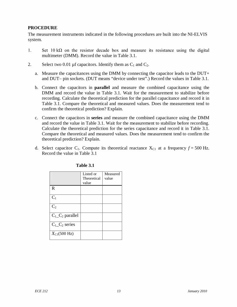
PROCEDURE
The measurement instruments indicated in the following procedures are built into the NI-ELVISsystem.
1. Set 10 kΩ on the resistor decade box and measure its resistance using the digital multimeter (DMM). Record the value in Table 3.1.
2. Select two 0.01 µf capacitors. Identify them as C1 and C2.
a. Measure the capacitances using the DMM by connecting the capacitor leads to the DUT+and DUT– pin sockets. (DUT means “device under test”.) Record the values in Table 3.1.
b. Connect the capacitors in parallel and measure the combined capacitance using theDMM and record the value in Table 3.1. Wait for the measurement to stabilize beforerecording. Calculate the theoretical prediction for the parallel capacitance and record it inTable 3.1. Compare the theoretical and measured values. Does the measurement tend toconfirm the theoretical prediction? Explain.
c. Connect the capacitors in series and measure the combined capacitance using the DMMand record the value in Table 3.1. Wait for the measurement to stabilize before recording.Calculate the theoretical prediction for the series capacitance and record it in Table 3.1.Compare the theoretical and measured values. Does the measurement tend to confirm thetheoretical prediction? Explain.
d. Select capacitor C1. Compute its theoretical reactance XC1 at a frequency f = 500 Hz.Record the value in Table 3.1
R
C1
C2
C1_C2 paral
C1_C2 series
XC1(500 Hz)
Table 3.1
Listed orTheoreticalvalue
Measuredvalue
lel
13 January 2010
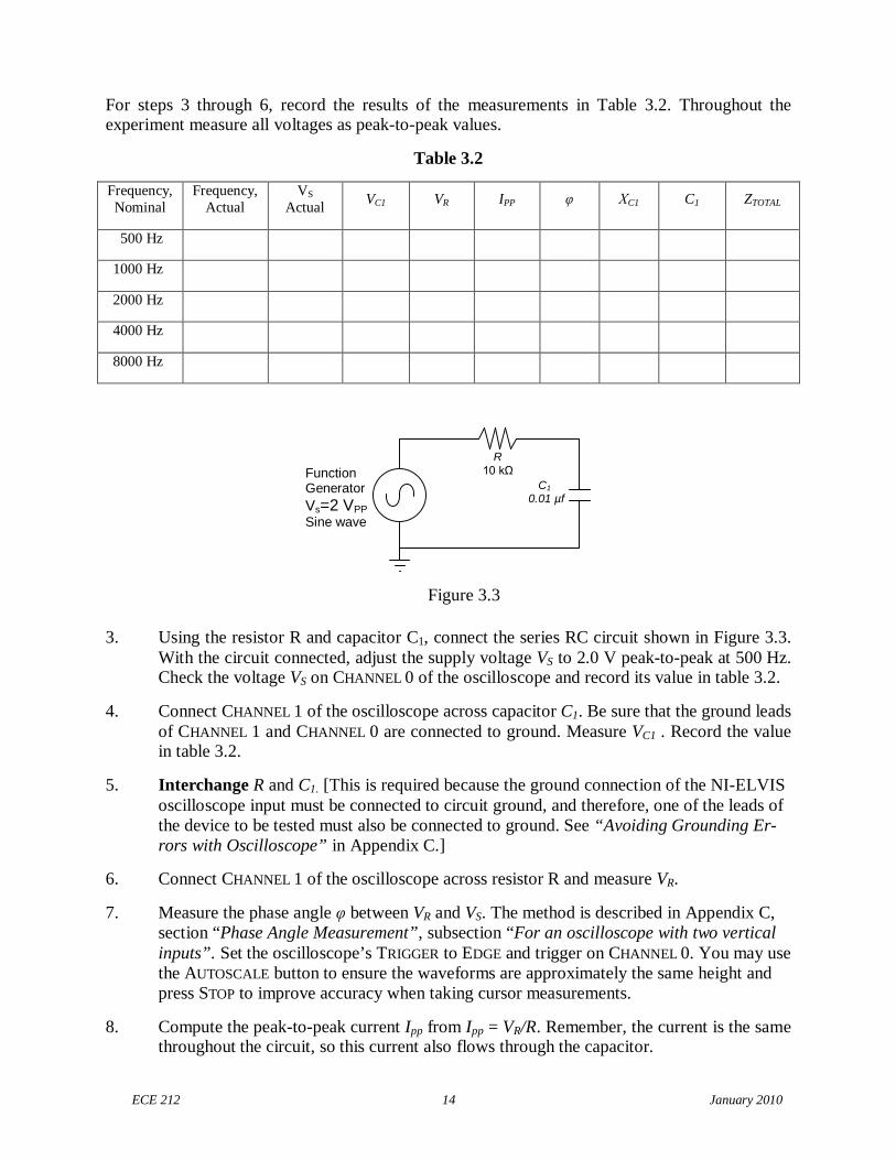
ECE 212 14 January 2010
For steps 3 through 6, record the results of the measurements in Table 3.2. Throughout theexperiment measure all voltages as peak-to-peak values.
Table 3.2
Frequency,Nominal
Frequency,Actual
VS
ActualVC1 VR IPP φ XC1 C1 ZTOTAL
500 Hz
1000 Hz
2000 Hz
4000 Hz
8000 Hz
3. Using the resistor R and capacitor C1, connect the series RC circuit shown in Figure 3.3.With the circuit connected, adjust the supply voltage VS to 2.0 V peak-to-peak at 500 Hz.Check the voltage VS on CHANNEL 0 of the oscilloscope and record its value in table 3.2.
4. Connect CHANNEL 1 of the oscilloscope across capacitor C1. Be sure that the ground leadsof CHANNEL 1 and CHANNEL 0 are connected to ground. Measure VC1 . Record the valuein table 3.2.
5. Interchange R and C1. [This is required because the ground connection of the NI-ELVISoscilloscope input must be connected to circuit ground, and therefore, one of the leads ofthe device to be tested must also be connected to ground. See “Avoiding Grounding Er-rors with Oscilloscope” in Appendix C.]
6. Connect CHANNEL 1 of the oscilloscope across resistor R and measure VR.
7. Measure the phase angle φ between VR and VS. The method is described in Appendix C,section “Phase Angle Measurement”, subsection “For an oscilloscope with two verticalinputs”. Set the oscilloscope’s TRIGGER to EDGE and trigger on CHANNEL 0. You may usethe AUTOSCALE button to ensure the waveforms are approximately the same height andpress STOP to improve accuracy when taking cursor measurements.
8. Compute the peak-to-peak current Ipp from Ipp = VR/R. Remember, the current is the samethroughout the circuit, so this current also flows through the capacitor.
Figure 3.3
R10 kΩ Function
Generator
Vs=2 VPP
Sine wave
C1
0.01 µf
ECE 212 15 January 2010
9. Compute the capacitor’s reactance XC1 from XC1 = VC1/IPP. Compute C1 from themeasured XC1 and compare to your earlier measurement.
10. Compute the total impedance ZTotal by applying Ohm’s law to the circuit. Use the supplyvoltage set in step 3 and the current found in step 4. Remember, the impedance has both amagnitude and a phase angle (measured relative to the resistor).
11. Repeat steps 3 to 10 (resetting VS if necessary) for the following frequencies: 1000, 2000,4000, 8000 Hz.
12. Draw impedance and voltage phasors (as in Figure 3.2) for frequency f = 1000 Hz.
13. Draw impedance and voltage phasors for frequency f = 4000 Hz.
14. The phasor diagrams at various frequencies show how the impedances, and therefore thevoltages, change with frequency. To better see the net effect on the circuit, graph VC1 andVR versus frequency for the values in Table 3.2. Label the curves.
PROBING FURTHER
1. Describe what happens to the current in this RC series circuit as the frequency increases.Explain in general terms why the observed change should occur.
2. Simulate the circuit in B2-SPICE and graph VC1 and VR versus frequency over the rangeof values in Table 3.2. Compare to your manually drawn curves. [Instructions for settingup the necessary AC simulation in B2-SPICE are shown in Appendix D.]
3. In this experiment it was shown that the voltage phasor diagram can be obtained by mul-tiplying each of the impedance phasors by the current in the circuit. If each of the voltagephasors in the voltage phasor diagram is again multiplied by the current, the resultingdiagram is the power phasor diagram. Using the data in Table 3.2 convert the current Iand source voltage VS to RMS values. Then draw a plot of the power phasor diagrams at afrequency of 1000 Hz and another at a frequency of 4000 Hz. Determine the real power,the reactive power, and the apparent power in the RC circuit at those frequencies.
REPORT: Your Laboratory Teaching Assistant will inform you when a report is due, and onwhich experiment you will report. Make sure that you have recorded all necessary informationand data in your laboratory notebook to enable you to prepare a report on this experiment, if sodirected, at some time in the future.
ECE 212 16 January 2010
Laboratory 4
Inductors and Series RL Circuits
INTRODUCTION: This laboratory continues the study of series linear circuits, this time look-ing at the effect of inductors in series linear circuits. Besides studying the behavior of induc-tors, you will use measurements of magnitude and phase to construct phasor diagrams for si-nusoidal voltages in a series circuit, and thereby validate Kirchhoff’s Voltage Law evenwhen the current varies with time.
EDUCATIONAL OBJECTIVES:(1) Learn to predict and to measure inductive reactance.(2) Learn to apply Ohm’s law to reactances of impedances.(3) Learn to measure phase angles between voltages.(4) Learn to draw impedance and voltage phasor diagrams for resistors and inductors in series.(5) Gain experience in the construction and use of phasor diagrams.
EXPERIMENTAL OBJECTIVES:(1) Determine the reactance of an inductor in a series RL circuit by measuring voltages.(2) Draw impedance and voltage phasor diagrams for a series RL circuit.(3) Determine the real, reactive, and apparent power for a series RL circuit.(4) Explain the effect of frequency on the impedance and voltage phasors for a series RL circuit.
PRE-LAB:
Reading:(1) Study the Background section of this Laboratory experiment.(2) Review Appendix C, especially Avoiding Grounding Errors with Oscilloscope, and
Phase-Angle Measurement for an oscilloscope with two vertical inputs.
Written:(1) In your lab notebook sketch the circuit diagram to be used in the procedure.(2) Prepare tables to record the data.(3) Sketch the impedance and voltage phasors diagrams (as in Figure 4.2) you would get at
10 kHz for the circuit in Figure 4.3, using nominal values for the components. Make a ta-ble of the magnitudes and phase angles. You will use this to check that your experimentalsetup is correct.
EQUIPMENT NEEDED:
NI-ELVIS II
Function generator
Oscilloscope
Digital Multimeter
Resistor, 5 kΩ
Inductor, 50 mHComponents may be discrete or via decade substitution boxes.
ECE 212 17 January 2010
BACKGROUND
When a current passes through a wire, a magnetic field is generated around the wire. The mag-netic field results from the movement of electric charge and is proportional to the magnitude ofthe current. Turning the wire into a coil concentrates that magnetic field, with the field of oneturn of the coil reinforcing another. Such a coil is called an inductor. From an electrical point ofview the especially interesting fact is that if the current in the wire changes, the magnetic fieldwill react to try to keep the current constant. This property of inductors is described by Lenz’slaw.
An inductor’s response to changes of current is called inductance. Inductance opposes changes incurrent, just as capacitance opposes changes in voltage. Inductance is the electric current equiva-lent of inertia in mechanical systems.
Inductance is measured in henries. One henry is the amount of inductance present when one voltis generated as a result of a current changing at the rate of one ampere per second.
When inductors are connected in series, the total inductance is the sum of the individual induc-tors. This is similar to the way resistors in series add. When inductors are connected in parallel,the inductances add in the same way that parallel resistors add. However, an additional effect canappear in inductance circuits that is not present with resistors. This effect is called mutual induc-tance and is caused by the interaction of the magnetic fields of neighboring inductors. Mutualinductance can either increase or decrease the total inductance, depending on the orientation ofthe interacting inductors.
Inductance circuits have a time constant associated with them, just as do capacitance circuits,except that the curve of interest for inductors is the current, rather than the voltage. The timeconstant τ for inductors is
L
R .
where τ is in seconds; L is in henries; R is in ohms.
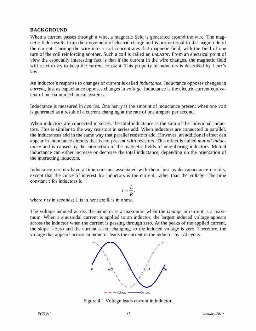
The voltage induced across the inductor is a maximum when the change in current is a maxi-mum. When a sinusoidal current is applied to an inductor, the largest induced voltage appearsacross the inductor when the current is passing through zero. At the peaks of the applied current,the slope is zero and the current is not changing, so the induced voltage is zero. Therefore, thevoltage that appears across an inductor leads the current in the inductor by 1/4 cycle.
0 π/2 π 3π/4 2π
Voltage Current
Figure 4.1 Voltage leads current in inductor.
ECE 212 18 January 2010
Inductive reactance
As the frequency of the sine wave increases, the rate of change of the current also increases, andso the induced (reacting) voltage across the inductor increases. As a result, the net currentthrough the inductor decreases. That means, the inductor’s reactance increases with frequency.The inductive reactance is given by
2LX f L
As with capacitors and resistors, Ohm’s law can be applied to inductive circuits:
LL
L
VX
I .
Series RL circuits
When a sine wave is applied to a series circuit of linear components (resistors, capacitors, andinductors), the phase relationships between current and voltage depend on the types of compo-nents. The current and voltage are always in phase across an ideal resistor. The current through acapacitor leads the voltage across the capacitor by 90°. The voltage across an ideal inductor leadsthe current through the inductor by 90°.
A common memory aid for these relationships is “ELI the ICE man”, where E represents volt-age (E is short for “electromotive force”, which is another term for voltage), I represents current,L represents inductance, and C represents capacitance.
From Kirchhoff’s current law (KCL), we know that the current is the same throughout a seriescircuit. Since the current and voltage are in phase for a resistor, we can determine the phase ofthe current by measuring the phase of the voltage across the resistor. This is commonly done byusing an oscilloscope to compare the voltage from the source to the voltage across the resistor.
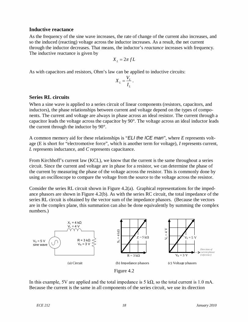
Consider the series RL circuit shown in Figure 4.2(a). Graphical representations for the imped-ance phasors are shown in Figure 4.2(b). As with the series RC circuit, the total impedance of theseries RL circuit is obtained by the vector sum of the impedance phasors. (Because the vectorsare in the complex plane, this summation can also be done equivalently by summing the complexnumbers.)
Figure 4.2
In this example, 5V are applied and the total impedance is 5 kΩ, so the total current is 1.0 mA. Because the current is the same in all components of the series circuit, we use its direction
VS = 5 Vsine wave
XL = 4 kΩ VL = 4 V
R = 3 kΩ VR = 3 V
VR = 3 V
Direction ofcurrent phasor(reference)
VS = 5 VVL
=4
V
Z = 5 kΩ
R = 3 kΩ
XL
=4
kΩ
(a) Circuit (b) Impedance phasors (c) Voltage phasors
ECE 212 19 January 2010
through the resistor for the phase reference direction. Multiplying the impedance phasors by thecurrent gives the voltage phasors, as shown in Figure 4.2(c).
In this experiment you will use an oscilloscope to measure the phase angles in the circuit. Be-cause of the resistance of the wires in an inductor, actual inductors may have enough resistanceto affect the phase angle. To minimize that effect in this experiment, we will use a series resistorthat is large compared to the inductor’s resistance.
SAFETY PRECAUTIONS
1. Always turn off power to the circuit when changing the circuit.
2. Only reapply power after verifying that the circuit is properly wired and that the voltage to beapplied is at or below the required value.
3. Failure to turn off power when making circuit changes is a major reason for blowing fuses inthe equipment, thereby rendering the equipment unusable and wasting your time and that ofothers. Please carefully check circuit wiring, resistor settings, and voltage settings before ap-plying power to the circuits.
PROCEDURE
The measurement instruments indicated in the following procedures are built into the NI-ELVISsystem. Use peak-to-peak readings for all voltage and current measurements in this experiment.
1. Construct a table for recording experimental data:
R L f VS (gen) VS (Osc) VR VL I XL ZT
φmeas φcalc
2. Select a 5 kΩ resistor or set that value on the resistor decade box. Measure its resistance using the digital multimeter (DMM) and record the measured value.
3. Select a 50 mH inductor or set that value on the inductor decade box. Measure its induc-tance L and winding resistance RW using the DMM and record the value. To measure in-ductance requires connecting the leads to DUT+ and DUT–, as you did for the capacitor.
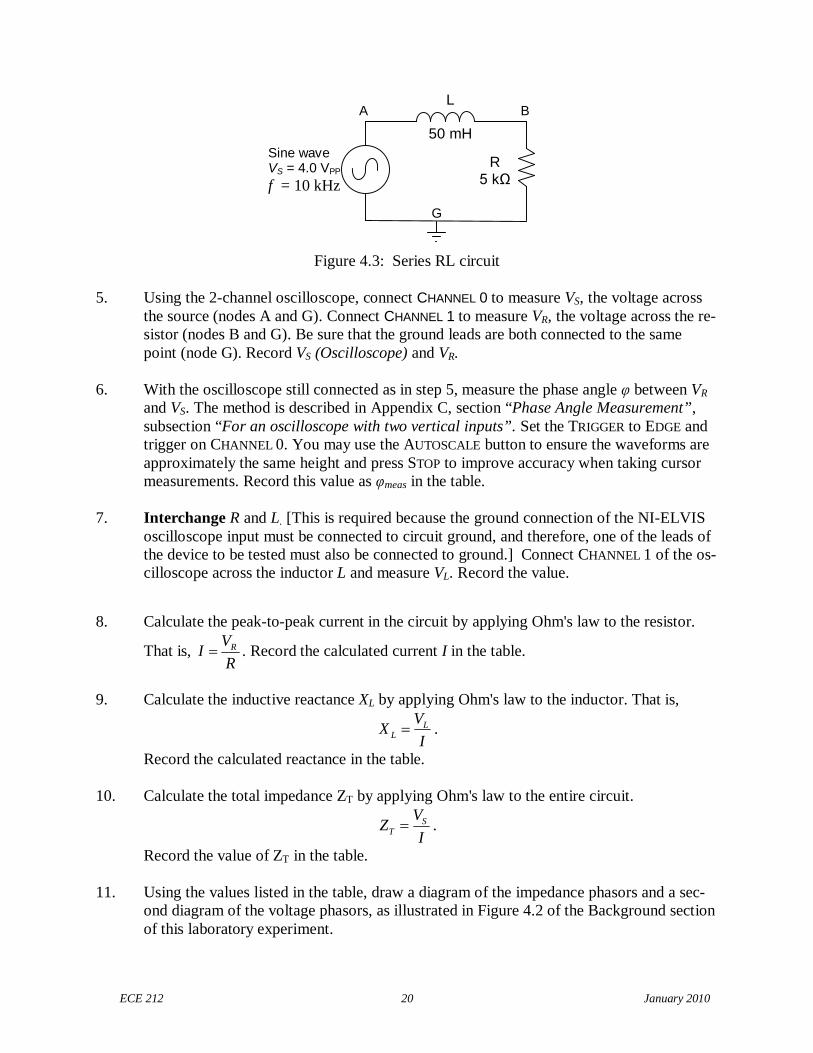
4. Construct the circuit shown in Figure 4.3. With the circuit connected, adjust the functiongenerator’s frequency f to 10 kHz with an output voltage of 4.0 VPP. Record the actualvalues of f and VS (generator).
ECE 212
Figure
5. Using the 2-channel oscilloscope,the source (nodes A and G). Connsistor (nodes B and G). Be sure thpoint (node G). Record VS (Oscillo
6. With the oscilloscope still connectand VS. The method is described insubsection “For an oscilloscope wtrigger on CHANNEL 0. You may uapproximately the same height andmeasurements. Record this value a
7. Interchange R and L. [This is requoscilloscope input must be connecthe device to be tested must also bcilloscope across the inductor L an
8. Calculate the peak-to-peak curren
That is, RVI
R . Record the calcul
9. Calculate the inductive reactance X
Record the calculated reactance in
10. Calculate the total impedance ZT b
Record the value of ZT in the table
11. Using the values listed in the tableond diagram of the voltage phasorof this laboratory experiment.
Sine waveVS = 4.0 VPP
f = 10 kHz
20
4.3: Series RL circuit
connect CHANNEL 0 to meect CHANNEL 1 to measureat the ground leads are boscope) and VR.
ed as in step 5, measure tAppendix C, section “P
ith two vertical inputs”. Sse the AUTOSCALE button
press STOP to improve as φmeas in the table.
ired because the groundted to circuit ground, ande connected to ground.] Cd measure VL. Record the
t in the circuit by applying
ated current I in the table
L by applying Ohm's law
LL
VX
I .
the table.
y applying Ohm's law to
ST
VZ
I .
.
, draw a diagram of the ims, as illustrated in Figure
L
50 mH
R5 kΩ
A B
G
January 2010
asure VS, the voltage acrossVR, the voltage across the re-
th connected to the same
he phase angle φ between VR
hase Angle Measurement”,et the TRIGGER to EDGE andto ensure the waveforms are
ccuracy when taking cursor
connection of the NI-ELVIStherefore, one of the leads ofonnect CHANNEL 1 of the os-value.
Ohm's law to the resistor.
.
to the inductor. That is,
the entire circuit.
pedance phasors and a sec-4.2 of the Background section
ECE 212 21 January 2010
12. Compute the phase angle φ between VS and VR. Recall that
arctan L
R
V
V
.
Record this value as φcalc in the table, and compare it to the value measured on the oscil-loscope.
13. Using the data in the table, convert the current I and source voltage VS to RMS values.Then draw plots of the power phasor diagrams at the frequency of 10k Hz. Determine thereal power, the reactive power, and the apparent power in the RL circuit at that fre-quency.
PROBING FURTHER
1. What you think would happen to the current in this RL series circuit if the frequencywere decreased, say, to 2000 Hz? Why?
2. Simulate the circuit in B2-SPICE and graph VL and VR versus frequency from 1000 Hz to20,000 Hz. Does the simulation support your prediction in question 1?
REPORT: Your Laboratory Teaching Assistant will inform you when a report is due, and onwhich experiment you will report. Make sure that you have recorded all necessary informationand data in your laboratory notebook to enable you to prepare a report on this experiment, if sodirected, at some time in the future.
ECE 212 22 January 2010
Laboratory 5
Parallel RC and RL Circuits
INTRODUCTION: This laboratory explores the behavior of parallel RC and RL circuits, andthe application of Kirchhoff’s current and voltage laws to such circuits. For series RC and RLcircuits, we saw that Kirchhoff’s voltage law applies, but that the voltages must be added asphasors. Similarly, in parallel circuits, Kirchhoff's current law applies to any junction, butagain, the currents must be added as phasors.
EDUCATIONAL OBJECTIVES:(1) Learn to apply Kirchhoff’s voltage law (KVL) and Kirchhoff’s current law (KCL) in parallel cir-
cuits.(2) Learn to draw current phasor diagrams for parallel circuits.(3) Gain experience in the construction and use of phasor diagrams.(4) Gain experience in calculating real, reactive, and apparent power.
EXPERIMENTAL OBJECTIVES:(1) Confirm Kirchhoff’s current law (KCL) in parallel circuits.(2) Draw current phasor diagrams for parallel circuits.(3) Determine the real, reactive, and apparent power for a parallel RC circuit.
PRE-LAB:
Reading:(1) Study the Background section of this Laboratory.
Written:(1) In your lab notebook sketch the circuit diagrams to be used in the procedure.(2) Prepare tables to record data.
EQUIPMENT NEEDED:
NI-ELVIS II
Function generator
Oscilloscope
Digital Multimeter
Resistor, 10 kΩ
Resistor, 2.2 kΩ
Resistor, 100 Ω, Qty. 2 (discrete)
Resistor, 22 Ω, Qty. 2 (discrete)
Inductor, 100 mH
Capacitor, 0.01 µFComponents may be discrete or via decade substitution boxes, unless otherwise indicated.
ECE 212 23 January 2010
BACKGROUND
As was seen in prior experiments, in a series circuit the same current is in all components, and socurrent is generally used as a reference in series circuits. However, in parallel circuits, the samevoltage is across all components, so voltage is the logical and appropriate reference. The currentin each branch then evolves from the circuit voltage.
For series RC and RL circuits, we saw that Kirchhoff’s voltage law applies, but that the voltagesmust be added as phasors. Similarly, in parallel circuits, Kirchhoff's current law applies to anyjunction, but again, the currents must be added as phasors. The current entering a junction is al-ways equal to the current leaving the junction.
In a parallel circuit, if the impedance of each branch is known, then the current in that branch canbe determined directly from the applied voltage and Ohm's law. The current phasor diagram canthen be constructed, and the total current can be found as the phasor sum of the currents in eachbranch.
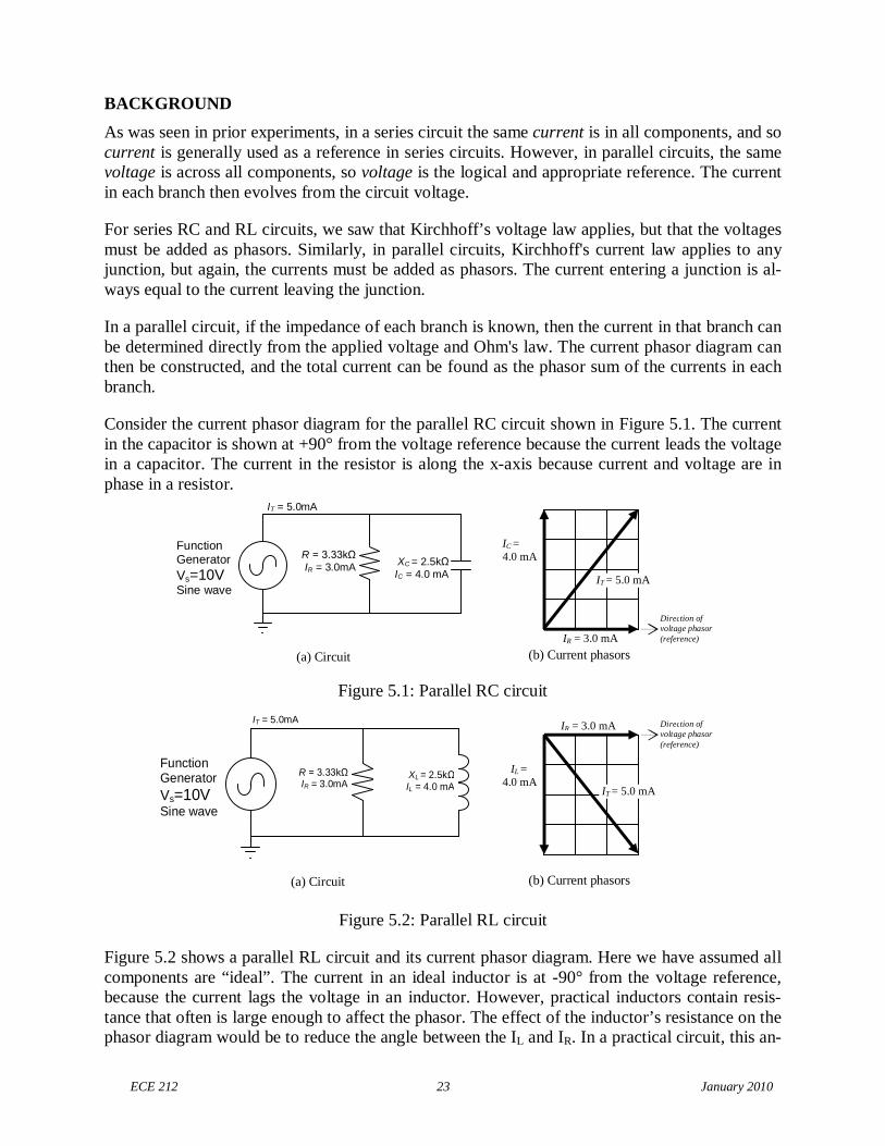
Consider the current phasor diagram for the parallel RC circuit shown in Figure 5.1. The currentin the capacitor is shown at +90° from the voltage reference because the current leads the voltagein a capacitor. The current in the resistor is along the x-axis because current and voltage are inphase in a resistor.
Figure 5.1: Parallel RC circuit
Figure 5.2: Parallel RL circuit
Figure 5.2 shows a parallel RL circuit and its current phasor diagram. Here we have assumed allcomponents are “ideal”. The current in an ideal inductor is at -90° from the voltage reference,because the current lags the voltage in an inductor. However, practical inductors contain resis-tance that often is large enough to affect the phasor. The effect of the inductor’s resistance on thephasor diagram would be to reduce the angle between the IL and IR. In a practical circuit, this an-
R = 3.33kΩIR = 3.0mA
FunctionGenerator
Vs=10VSine wave
XC = 2.5kΩIC = 4.0 mA
IT = 5.0mA
(a) Circuit
IC =4.0 mA
(b) Current phasors
Direction ofvoltage phasor(reference)IR = 3.0 mA
IT = 5.0 mA
R = 3.33kΩIR = 3.0mA
FunctionGenerator
Vs=10VSine wave
XL = 2.5kΩIL = 4.0 mA
IT = 5.0mA
(a) Circuit
IL =4.0 mA
(b) Current phasors
Direction ofvoltage phasor(reference)
IR = 3.0 mA
IT = 5.0 mA
ECE 212 24 January 2010
gle will be slightly less than the -90° of a pure inductor. This experiment will illustrate this dif-ference between the approximation of circuit performance based on ideal components and theactual measured values.
For both RC and RL circuits, the Pythagorean theorem and ordinary vector addition can be ap-plied to the current phasors to determine the magnitude of the total current, IT.
2 2 2 2T R C T R LI I I and I I I .
Recall that in series circuits, the phase angle was measured between the source voltage VS andthe resistor voltage VR using the oscilloscope. The oscilloscope is a voltage-sensitive device, soexamining those voltages and phase angles is straightforward. But in parallel circuits, the phaseangle of interest usually is between the total current, IT, and one of the branch currents. To usethe oscilloscope to measure the phase angle in a parallel circuit, we must convert the current to avoltage. This is commonly done by inserting a small resistor (a "sense" resistor) in the branchwith the current to be measured. Such a sense resistor makes it easy to determine the magnitudeand the phase of the current in that branch, but the resistor must be small enough not to have asignificant effect on the values to be measured.
PROCEDURE
Parallel RC Circuit
This part of the experiment will give you experience making the measurements with the digi-tal multimeter (DMM). Because the electrodes of this device are isolated from the circuitground and the grounds in NI-ELVIS, you may make voltage measurements directly acrossany of the components, whether or not they are grounded.
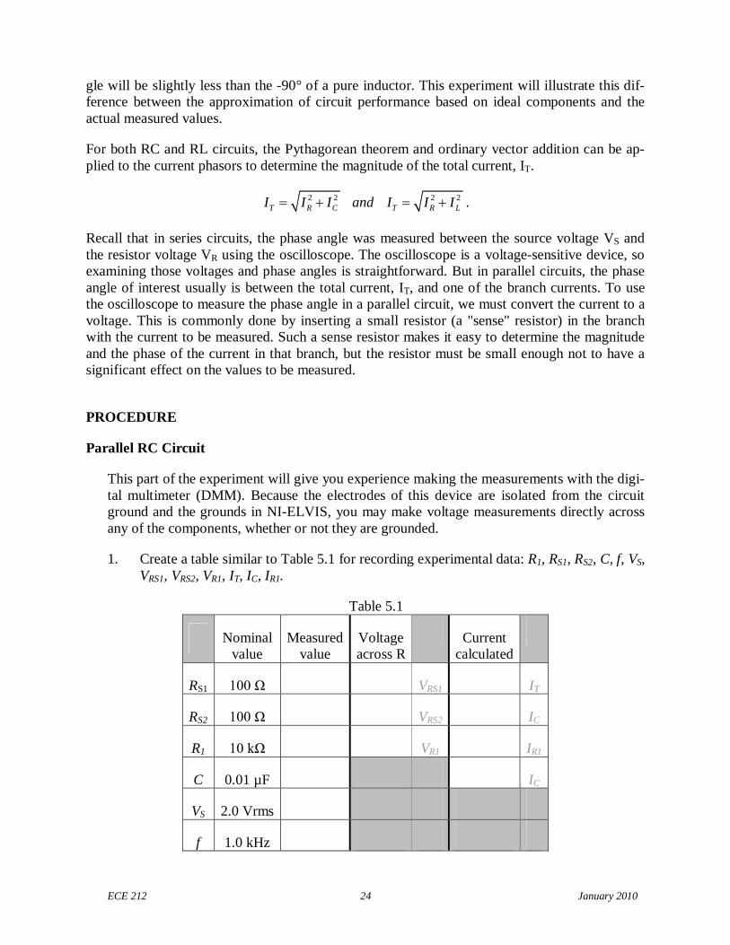
1. Create a table similar to Table 5.1 for recording experimental data: R1, RS1, RS2, C, f, VS,VRS1, VRS2, VR1, IT, IC, IR1.
Table 5.1
Nominalvalue
Measuredvalue
Voltageacross R
Currentcalculated
RS1 100 Ω VRS1 IT
RS2 100 Ω VRS2 IC
R1 10 kΩ VR1 IR1
C 0.01 µF IC
VS 2.0 Vrms
f 1.0 kHz
ECE 212 25 January 2010
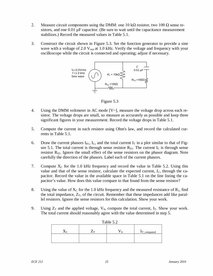
2. Measure circuit components using the DMM: one 10 kΩ resistor, two 100 Ω sense re-sistors, and one 0.01 µF capacitor. (Be sure to wait until the capacitance measurementstabilizes.) Record the measured values in Table 5.1.
3. Construct the circuit shown in Figure 5.3. Set the function generator to provide a sinewave with a voltage of 2.0 Vrms at 1.0 kHz. Verify the voltage and frequency with youroscilloscope while the circuit is connected and operating; adjust if necessary.
Figure 5.3
4. Using the DMM voltmeter in AC mode [V~], measure the voltage drop across each re-sistor. The voltage drops are small, so measure as accurately as possible and keep threesignificant figures in your measurement. Record the voltage drops in Table 5.1.
5. Compute the current in each resistor using Ohm's law, and record the calculated cur-rents in Table 5.1.
6. Draw the current phasors IR1, IC, and the total current IT in a plot similar to that of Fig-ure 5.1. The total current is through sense resistor RS1. The current IC is through senseresistor RS2. Ignore the small effect of the sense resistors on the phasor diagram. Notecarefully the direction of the phasors. Label each of the current phasors.
7. Compute XC for the 1.0 kHz frequency and record the value in Table 5.2. Using thisvalue and that of the sense resistor, calculate the expected current, IC, through the ca-pacitor. Record the value in the available space in Table 5.1 on the line listing the ca-pacitor’s value. How does this value compare to that found from the sense resistor?
8. Using the value of XC for the 1.0 kHz frequency and the measured resistance of R1, findthe total impedance, ZT, of the circuit. Remember that these impedances add like paral-lel resistors. Ignore the sense resistors for this calculation. Show your work.
9. Using ZT and the applied voltage, VS, compute the total current, IT. Show your work.The total current should reasonably agree with the value determined in step 5.
Table 5.2
XC ZT VS IT_computed
R1 = 10kΩ
Vs=2.0Vrmsf =1.0 kHzSine wave
C0.01 µF
RS1 =100Ω
RS2 =100Ω
ECE 212 26 January 2010
10. Change the frequency to 2.0 kHz at 2.0 Vrms. Repeat steps 4, 5, and 6, recording the re-sults in a separate table.
PROBING FURTHER
1. Ignoring the effect of the sense resistors, compute the real, reactive, and apparent powerof the circuit in Figure 5.3 at 1.0 kHz and at 2.0 kHz.
2. Explain how increasing the frequency affected (a) the total impedance of the circuit,and (b) the phase angle between the function generator's voltage and the function gen-erator's current.
3. If the capacitor C were made smaller, what would happen to the current phasor dia-grams?
Parallel RL Circuit
This part of the experiment will give you experience making similar measurements using theoscilloscope. Remember that the ground lead of the oscilloscope must be connected to circuitground, that is, the ground of the function generator, in this case. Do not try to make meas-urements directly across ungrounded components.
Also, in this part of the experiment, record all voltages and currents as peak-to-peak values.
1. Create a table similar to Table 5.3 for recording experimental data: R1, RS1, RS2, L, f, VS,VRS1, VRS2, VR1, IT, IL, IR1.
Table 5.3
Nominalvalue
Measuredvalue
Voltageacross R
Currentcalculated
RS1 22 Ω VRS1 IT
RS2 22 Ω VRS2 IL
R1 2.2 kΩ VR1 IR1
L 100 mH IL
VS 4.0 VPP
f 4.0 kHz
2. Using the DMM, measure the actual values of a 2.2 kΩ resistor, two 22 ohm resistors, and a 100 mH inductor.
3. Measure the winding resistance of the inductor, RW, with an ohmmeter.
ECE 212 27 January 2010
Figure 5.4
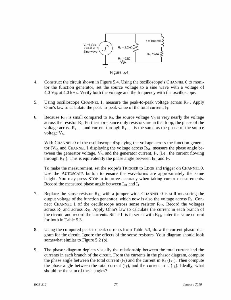
4. Construct the circuit shown in Figure 5.4. Using the oscilloscope’s CHANNEL 0 to moni-tor the function generator, set the source voltage to a sine wave with a voltage of4.0 VPP at 4.0 kHz. Verify both the voltage and the frequency with the oscilloscope.
5. Using oscilloscope CHANNEL 1, measure the peak-to-peak voltage across RS1. ApplyOhm's law to calculate the peak-to-peak value of the total current, IT.
6. Because RS1 is small compared to R1, the source voltage VS is very nearly the voltageacross the resistor R1. Furthermore, since only resistors are in that loop, the phase of thevoltage across R1 — and current through R1 — is the same as the phase of the sourcevoltage VS.
With CHANNEL 0 of the oscilloscope displaying the voltage across the function genera-tor (VS), and CHANNEL 1 displaying the voltage across RS1, measure the phase angle be-tween the generator voltage, VS, and the generator current, IT, (i.e., the current flowingthrough RS1). This is equivalently the phase angle between IR1 and IT.
To make the measurement, set the scope’s TRIGGER to EDGE and trigger on CHANNEL 0.Use the AUTOSCALE button to ensure the waveforms are approximately the sameheight. You may press STOP to improve accuracy when taking cursor measurements.Record the measured phase angle between IR1 and IT.
7. Replace the sense resistor RS1 with a jumper wire. CHANNEL 0 is still measuring theoutput voltage of the function generator, which now is also the voltage across R1. Con-nect CHANNEL 1 of the oscilloscope across sense resistor RS2. Record the voltagesacross R1 and across RS2. Apply Ohm's law to calculate the current in each branch ofthe circuit, and record the currents. Since L is in series with RS2, enter the same currentfor both in Table 5.3.
8. Using the computed peak-to-peak currents from Table 5.3, draw the current phasor dia-gram for the circuit. Ignore the effects of the sense resistors. Your diagram should looksomewhat similar to Figure 5.2 (b).
9. The phasor diagram depicts visually the relationship between the total current and thecurrents in each branch of the circuit. From the currents in the phasor diagram, computethe phase angle between the total current (IT) and the current in R1 (IR1). Then computethe phase angle between the total current (IT), and the current in L (IL). Ideally, whatshould be the sum of these angles?
R1 = 2.2kΩVs=4 Vppf =4.0 kHzSine wave
L = 100 mH
RS1 =22Ω
RS2 =22Ω

ECE 212 28 January 2010
10. On the oscilloscope, measure the angle between IL and IR1. (The oscilloscope’s leadswere already connected to do this as a result of step 7.) Ideally, this measurementshould be 90°, but resistance in the inductor, may reduce the angle. If necessary, adjustboth scope channels to have the same apparent height on the oscilloscope screen in or-der to make the measurement.
11. In step 6 you measured the phase angle ΦRT between IR1 and IT. In step 10 you meas-ured the phase angle ΦRL between IR1 and IL. Compute the phase angle ΦTL between IT
and IL by subtracting ΦRT from ΦRL. That is, ΦTL = ΦRL – ΦRT.
12. Construct a table that will allow easy comparison of the computed and measured phaseangles from steps 6, 9, 10, and 11. Compare the measured phase angles versus the com-puted phase angles. Discuss likely causes for any discrepancies.
PROBING FURTHER
1. The currents IR1 and IL were measured in step 7. If those currents are 90° apart, we can
calculate the total current IT using the Pythagorean theorem: 2 21T R LI I I .
a. Compare this calculated total current to the total current measured in step 5.
b. What factors might cause any discrepancies observed between the values?
2. What effect does the inductor’s coil resistance have on the phase angle between the cur-rents in the resistor and the inductor?
REPORT: Your Laboratory Teaching Assistant will inform you when a report is due, and onwhich experiment you will report. Make sure that you have recorded all necessary informationand data in your laboratory notebook to enable you to prepare a report on this experiment, if sodirected, at some time in the future.
ECE 212 29 January 2010
Laboratory 6
Circuit Resonance
INTRODUCTION: The response of a circuit containing both inductors and capacitors in seriesor in parallel depends on the frequency of the driving voltage or current. This laboratory willexplore one of the more dramatic effects of the interplay of capacitance and inductance,namely, resonance, when the inductive and capacitive reactances cancel each other. Reso-nance is the fundamental principle upon which most filters are based — filters that allow usto tune radios, televisions, cell phones, and a myriad of other devices deemed essential formodern living.
EDUCATIONAL OBJECTIVES:(1) Learn the definition of resonance in AC circuits.(2) Learn to calculate resonant frequencies, band widths, and quality factors for series and
parallel resonant circuits.(3) Learn to use NI-ELVIS’s Bode plot function to view circuit response.
EXPERIMENTAL OBJECTIVES:(1) Predict resonant frequencies, band widths, and quality factors for series resonant circuits.(2) Measure resonant frequencies, band widths, and quality factors for series resonant cir-
cuits, and compare them to predicted value.(3) Determine what effect changing the series resistance has on the resonance.
PRE-LAB:
Reading:(1) Study the Background section of this Laboratory exercise.
Written:(1) In your lab notebook sketch the circuit diagram to be used in the procedure.(2) Prepare tables to record data.
EQUIPMENT NEEDED:
NI-ELVIS II
Function generator
Oscilloscope
Digital Multimeter
Bode analyzer
Resistor, 100 Ω
Resistor, 10 Ω
Inductor, 100 mH
Capacitor, 0.01 µFComponents may be discrete or via decade substitution boxes, unless otherwise indicated.
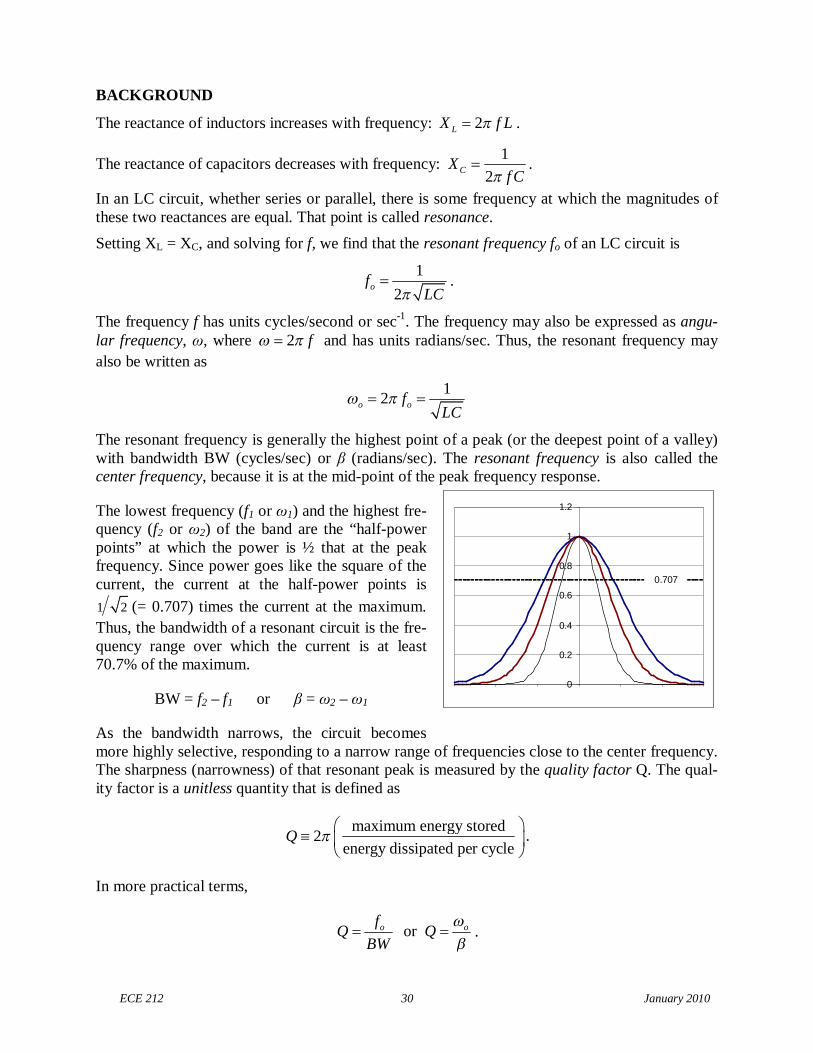
ECE 212 30 January 2010
BACKGROUND
The reactance of inductors increases with frequency: 2LX f L .
The reactance of capacitors decreases with frequency:1
2CX
f C .
In an LC circuit, whether series or parallel, there is some frequency at which the magnitudes ofthese two reactances are equal. That point is called resonance.
Setting XL = XC, and solving for f, we find that the resonant frequency fo of an LC circuit is
1
2of
LC .
The frequency f has units cycles/second or sec-1. The frequency may also be expressed as angu-lar frequency, ω, where 2 f and has units radians/sec. Thus, the resonant frequency may
also be written as
12o of
LC
The resonant frequency is generally the highest point of a peak (or the deepest point of a valley)with bandwidth BW (cycles/sec) or β (radians/sec). The resonant frequency is also called thecenter frequency, because it is at the mid-point of the peak frequency response.
The lowest frequency (f1 or ω1) and the highest fre-quency (f2 or ω2) of the band are the “half-powerpoints” at which the power is ½ that at the peakfrequency. Since power goes like the square of thecurrent, the current at the half-power points is
1 2 (= 0.707) times the current at the maximum.
Thus, the bandwidth of a resonant circuit is the fre-quency range over which the current is at least70.7% of the maximum.
BW = f2 – f1 or β = ω2 – ω1
As the bandwidth narrows, the circuit becomesmore highly selective, responding to a narrow range of frequencies close to the center frequency.The sharpness (narrowness) of that resonant peak is measured by the quality factor Q. The qual-ity factor is a unitless quantity that is defined as
maximum energy stored2
energy dissipated per cycleQ
.
In more practical terms,
oro ofQ Q
BW
.
0
0.2
0.4
0.6
0.8
1
1.2
-3 -2 -1 0 1 2 3
0.707
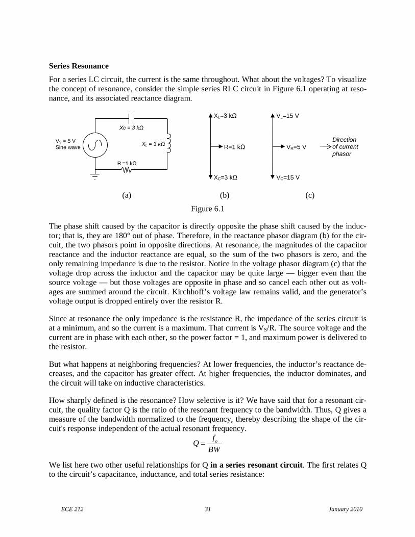
ECE 212 31
Series Resonance
For a series LC circuit, the current is the same throughout. What about the voltages? To visualizethe concept of resonance, consider the simple series RLC circuit in Figure 6.1 operating at reso-nance, and its associated reactance diagram.
(a) (b
Figure 6.1
The phase shift caused by the capacitor is directly optor; that is, they are 180° out of phase. Therefore, in tcuit, the two phasors point in opposite directions. Atreactance and the inductor reactance are equal, so thonly remaining impedance is due to the resistor. Noticvoltage drop across the inductor and the capacitor msource voltage — but those voltages are opposite in pages are summed around the circuit. Kirchhoff’s voltvoltage output is dropped entirely over the resistor R.
Since at resonance the only impedance is the resistanat a minimum, and so the current is a maximum. Thatcurrent are in phase with each other, so the power factthe resistor.
But what happens at neighboring frequencies? At lowcreases, and the capacitor has greater effect. At highethe circuit will take on inductive characteristics.
How sharply defined is the resonance? How selectivecuit, the quality factor Q is the ratio of the resonant frmeasure of the bandwidth normalized to the frequenccuit's response independent of the actual resonant freq
ofQBW
We list here two other useful relationships for Q in ato the circuit’s capacitance, inductance, and total serie
XL=3 kΩ
XC=
Xc = 3 kΩ
VS = 5 VSine wave
XL = 3 kΩ
R =1 kΩ
VL=15 V
Direction
R=1 kΩ VR=5 V of currentphasor
January 2010
) (c)
posite the phase shift caused by the induc-he reactance phasor diagram (b) for the cir-resonance, the magnitudes of the capacitore sum of the two phasors is zero, and thee in the voltage phasor diagram (c) that theay be quite large — bigger even than thehase and so cancel each other out as volt-
age law remains valid, and the generator’s
ce R, the impedance of the series circuit iscurrent is VS/R. The source voltage and theor = 1, and maximum power is delivered to
er frequencies, the inductor’s reactance de-r frequencies, the inductor dominates, and
is it? We have said that for a resonant cir-equency to the bandwidth. Thus, Q gives ay, thereby describing the shape of the cir-uency.
series resonant circuit. The first relates Qs resistance:
3 kΩ VC=15 V

ECE 212 32 January 2010
1 LQ
R C .
The value of R in this equation is the total equivalent series resistance in the circuit. This formof the equation makes it easy to see ways to optimize the Q for the desired circuit. Decreasing R,increasing inductance, or decreasing capacitance will all tend to make Q larger and increase thecircuit's selectivity.
The second useful relationship for Q can be derived from the previous equation. Recall thatXL = 2πfL and XC = 1/2πfC. Then the previous equation can be rewritten as
1L CQ X X
R
Since at resonance the inductive and capacitive reactances are equal, this equation can be re-duced to
or CL XXQ Q
R R
where R is again the total equivalent series resistance of the circuit. Usually the XL form is usedbecause the resistance of the inductor frequently is the dominant resistance in the circuit.
An equivalent form of this last equation is
2 1or
2o
o
f LQ Q
R f CR
.
Parallel Resonance
For a parallel RLC circuit, the same voltage is applied across all the branches. The current ineach branch is determined by the voltage applied to the branch and the impedance in that branch.
A parallel RLC circuit with ideal components is illustrated below, along with its current phasordiagram. Notice that the total source current at resonance is the current in the resistor. The cur-rents in the inductor and capacitor cancel out because of their opposite phase shifts. The net im-pedance of the circuit at resonance is solely determined by R, since the inductor and the capaci-tor appear to be open.
Figure 6.2
In an ideal two-branch LC circuit including an inductor and capacitor (i.e., R is removed orequivalently R=∞), the source current would be zero. In a practical two-branch LC circuit, theonly significant resistance is the inductor’s winding resistance, so that resistance often plays animportant role in the circuit’s behavior.
IC = 3 mA
IL = 3 mA
IR = 1 mA
Direction ofvoltagephasor
(reference)
IC = 3 mA
IL = 3 mA
IR = 1 mA
R = 6 kΩIR = 1 mA
Vs= 6VSine wave
XL = 2 kΩIL = 3 mA
XC = 2 kΩIC = 3 mA
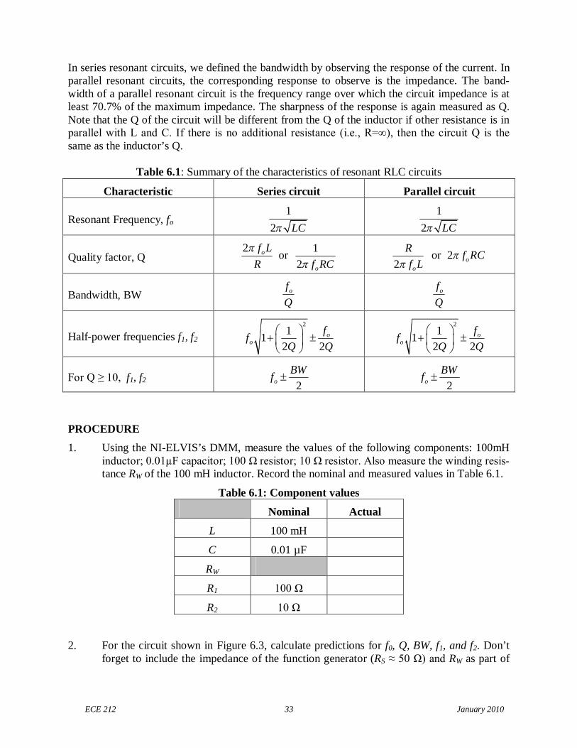
ECE 212 33 January 2010
In series resonant circuits, we defined the bandwidth by observing the response of the current. Inparallel resonant circuits, the corresponding response to observe is the impedance. The band-width of a parallel resonant circuit is the frequency range over which the circuit impedance is atleast 70.7% of the maximum impedance. The sharpness of the response is again measured as Q.Note that the Q of the circuit will be different from the Q of the inductor if other resistance is inparallel with L and C. If there is no additional resistance (i.e., R=∞), then the circuit Q is the same as the inductor’s Q.
Table 6.1: Summary of the characteristics of resonant RLC circuits
Characteristic Series circuit Parallel circuit
Resonant Frequency, fo
1
2 LC
1
2 LC
Quality factor, Q2 1
or2
o
o
f L
R f RC
or 2
2o
o
Rf RC
f L
Bandwidth, BWof
Qof
Q
Half-power frequencies f1, f2
21
12 2
oo
ff
Q Q
21
12 2
oo
ff
Q Q
For Q ≥ 10, f1, f22
o
BWf
2o
BWf
PROCEDURE
1. Using the NI-ELVIS’s DMM, measure the values of the following components: 100mHinductor; 0.01µF capacitor; 100 Ω resistor; 10 Ω resistor. Also measure the winding resis-tance RW of the 100 mH inductor. Record the nominal and measured values in Table 6.1.
Table 6.1: Component values
Nominal Actual
L 100 mH
C 0.01 µF
RW
R1 100 Ω
R2 10 Ω
2. For the circuit shown in Figure 6.3, calculate predictions for f0, Q, BW, f1, and f2. Don’tforget to include the impedance of the function generator (RS ≈ 50 Ω) and RW as part of
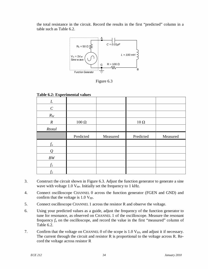
ECE 212 34 January 2010
the total resistance in the circuit. Record the results in the first “predicted” column in atable such as Table 6.2.
Figure 6.3
Table 6.2: Experimental values
L
C
RW
R 100 Ω 10 Ω
Rtotal
Predicted Measured Predicted Measured
fo
Q
BW
f1
f2
3. Construct the circuit shown in Figure 6.3. Adjust the function generator to generate a sinewave with voltage 1.0 VPP. Initially set the frequency to 1 kHz.
4. Connect oscilloscope CHANNEL 0 across the function generator (FGEN and GND) andconfirm that the voltage is 1.0 VPP.
5. Connect oscilloscope CHANNEL 1 across the resistor R and observe the voltage.
6. Using your predicted values as a guide, adjust the frequency of the function generator totune for resonance, as observed on CHANNEL 1 of the oscilloscope. Measure the resonantfrequency fo on the oscilloscope, and record the value in the first “measured” column ofTable 6.2.
7. Confirm that the voltage on CHANNEL 0 of the scope is 1.0 VPP, and adjust it if necessary.The current through the circuit and resistor R is proportional to the voltage across R. Re-cord the voltage across resistor R
C = 0.01µF
VS = 1VPP
Sine w ave
L = 100 mH
R = 100 Ω
RS = 50 Ω
Function Generator
A
G
B
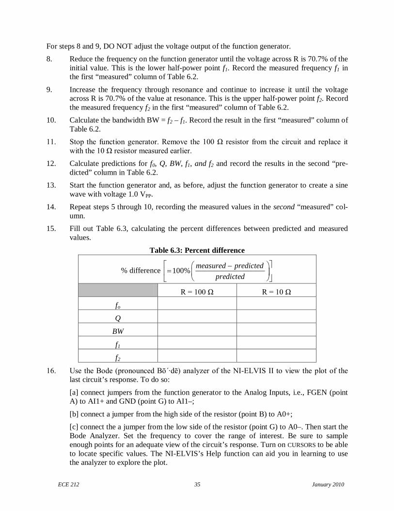
ECE 212 35 January 2010
For steps 8 and 9, DO NOT adjust the voltage output of the function generator.
8. Reduce the frequency on the function generator until the voltage across R is 70.7% of theinitial value. This is the lower half-power point f1. Record the measured frequency f1 inthe first “measured” column of Table 6.2.
9. Increase the frequency through resonance and continue to increase it until the voltageacross R is 70.7% of the value at resonance. This is the upper half-power point f2. Recordthe measured frequency f2 in the first “measured” column of Table 6.2.
10. Calculate the bandwidth BW = f2 – f1. Record the result in the first “measured” column ofTable 6.2.
11. Stop the function generator. Remove the 100 Ω resistor from the circuit and replace it with the 10 Ω resistor measured earlier.
12. Calculate predictions for f0, Q, BW, f1, and f2 and record the results in the second “pre-dicted” column in Table 6.2.
13. Start the function generator and, as before, adjust the function generator to create a sinewave with voltage 1.0 VPP.
14. Repeat steps 5 through 10, recording the measured values in the second “measured” col-umn.
15. Fill out Table 6.3, calculating the percent differences between predicted and measuredvalues.
Table 6.3: Percent difference
% difference 100%measured predicted
predicted
R = 100 Ω R = 10 Ω
fo
Q
BW
f1
f2
16. Use the Bode (pronounced Bō´·dē) analyzer of the NI-ELVIS II to view the plot of the last circuit’s response. To do so:
[a] connect jumpers from the function generator to the Analog Inputs, i.e., FGEN (pointA) to AI1+ and GND (point G) to AI1–;
[b] connect a jumper from the high side of the resistor (point B) to A0+;
[c] connect the a jumper from the low side of the resistor (point G) to A0–. Then start theBode Analyzer. Set the frequency to cover the range of interest. Be sure to sampleenough points for an adequate view of the circuit’s response. Turn on CURSORS to be ableto locate specific values. The NI-ELVIS’s Help function can aid you in learning to usethe analyzer to explore the plot.
ECE 212 36 January 2010
PROBING FURTHER
1. From the measured L, C, fo, and BW, compute the total series resistance of the circuit.Suggest and explain likely causes for any discrepancy; what might not have been takeninto account for the predictions?
2. Discuss the effect of changing the resistor R from 100 Ω to 10 Ω. How dramatic was the impact?
3. What would happen to the resonant frequency if the inductance were doubled and the ca-pacitance cut in half? What would happen to the bandwidth? What would happen to thequality factor?
4. Simulate the second circuit (with R=10Ω) in B2-SPICE, using the AC Frequency Sweep (see Appendix D). In the simulation, set up a voltmeter across R and an ammeter tomeasure the total current. Be sure to have B2-SPICE display both graphs and a table ofthe results. Select an appropriate range of frequencies to sweep and sample at least 100steps per interval. When the graph is displayed, right-click the graph and toggle the X-axis to be logarithmic. Do you see a sharp peak in the magnitude (dB) plots of voltageand current at the resonant frequency you predicted? Notice that the phase plot for thecircuit rapidly changes from positive (capacitive) to negative (inductive) as the frequencypasses through resonance. Record the resonant frequency indicated by the graph, andcompare it to your calculated and measured values.
REPORT: Your Laboratory Teaching Assistant will inform you when a report is due, and onwhich experiment you will report. Make sure that you have recorded all necessary informationand data in your laboratory notebook to enable you to prepare a report on this experiment, if sodirected, at some time in the future.
ECE 212 37 January 2010
Laboratory 7
Filters: High-pass, Low-pass, Bandpass, and Notch
INTRODUCTION: This laboratory studies the use of passive components to create filters toseparate portions of time-dependant waveforms. Filters are an essential tool in our complexworld of mixed signals — both electronic and otherwise. Passive components (resistors, ca-pacitors, and inductors) have long served as filter components for everything from selectingradio stations to filtering out electrical noise.
EDUCATIONAL OBJECTIVES:(1) Learn the four general filter types: High-pass, Low-pass, Bandpass, and Notch(2) Learn to alter filter type by changing contacts for output voltage.(3) Learn phase angle at cutoff for simple RC and RL filters.(4) Design simple filter.(5) Gain experience with Bode Analyzer and Bode Plots.
EXPERIMENTAL OBJECTIVES:(1) Calculate and measure cutoff frequency for series RC and RL filters.(2) Design simple RL low-pass filter.(3) Generate and interpret Bode plots for series filters.(4) Observe behavior of a single circuit used as a bandpass filter and as a notch filter.
PRE-LAB:
Reading:(1) Study the Background section of this Laboratory.(2) Study textbook regarding origin and meaning of “decibels”.
Written:(1) In your lab notebook sketch the circuit diagrams to be used in the procedure.(2) Perform the design calculations for the filter for Procedure 2.(3) Construct tables suitable for recording data where necessary, especially in Procedure 1.
EQUIPMENT NEEDED:
NI-ELVIS II
Function generator
Oscilloscope
Bode Analyzer
Digital MultimeterNote: Suitable Decade Substitution boxes may be used for the following components:
Resistors: 10 kΩ, 100 Ω, and a resistor to be determined
Inductor: 100 mH
Capacitor: 0.005 µF, 0.01 µF
BACKGROUND
In many circuits, a wide range of different frequencies are present, some of which are desired,while others are not. The frequency response of capacitors and inductors allows us to construct
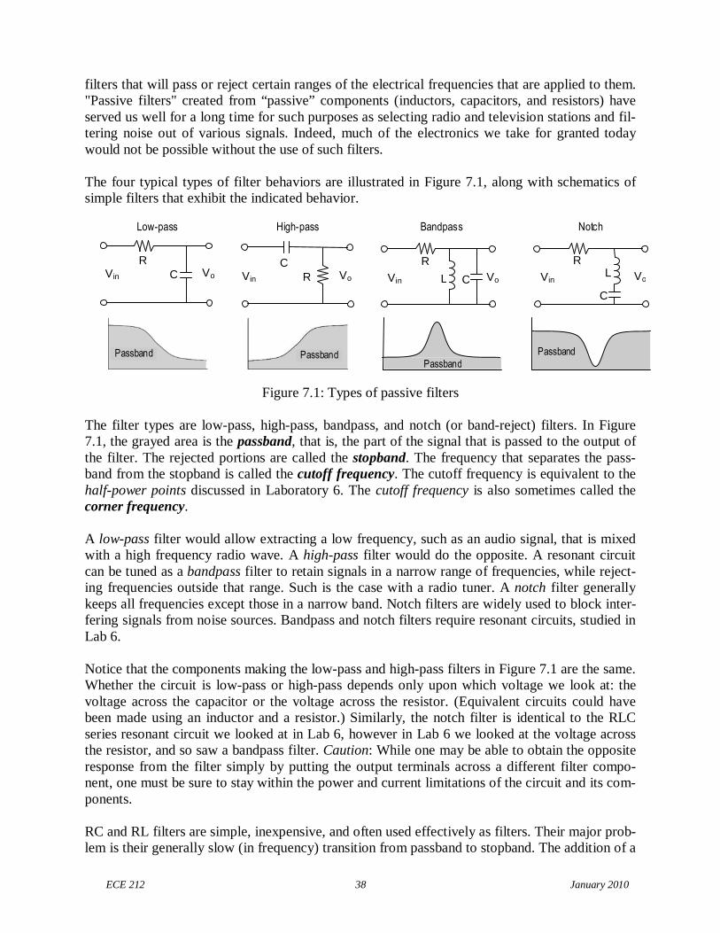
ECE 212 38 January 2010
filters that will pass or reject certain ranges of the electrical frequencies that are applied to them."Passive filters" created from “passive” components (inductors, capacitors, and resistors) haveserved us well for a long time for such purposes as selecting radio and television stations and fil-tering noise out of various signals. Indeed, much of the electronics we take for granted todaywould not be possible without the use of such filters.
The four typical types of filter behaviors are illustrated in Figure 7.1, along with schematics ofsimple filters that exhibit the indicated behavior.
Figure 7.1: Types of passive filters
The filter types are low-pass, high-pass, bandpass, and notch (or band-reject) filters. In Figure7.1, the grayed area is the passband, that is, the part of the signal that is passed to the output ofthe filter. The rejected portions are called the stopband. The frequency that separates the pass-band from the stopband is called the cutoff frequency. The cutoff frequency is equivalent to thehalf-power points discussed in Laboratory 6. The cutoff frequency is also sometimes called thecorner frequency.
A low-pass filter would allow extracting a low frequency, such as an audio signal, that is mixedwith a high frequency radio wave. A high-pass filter would do the opposite. A resonant circuitcan be tuned as a bandpass filter to retain signals in a narrow range of frequencies, while reject-ing frequencies outside that range. Such is the case with a radio tuner. A notch filter generallykeeps all frequencies except those in a narrow band. Notch filters are widely used to block inter-fering signals from noise sources. Bandpass and notch filters require resonant circuits, studied inLab 6.
Notice that the components making the low-pass and high-pass filters in Figure 7.1 are the same.Whether the circuit is low-pass or high-pass depends only upon which voltage we look at: thevoltage across the capacitor or the voltage across the resistor. (Equivalent circuits could havebeen made using an inductor and a resistor.) Similarly, the notch filter is identical to the RLCseries resonant circuit we looked at in Lab 6, however in Lab 6 we looked at the voltage acrossthe resistor, and so saw a bandpass filter. Caution: While one may be able to obtain the oppositeresponse from the filter simply by putting the output terminals across a different filter compo-nent, one must be sure to stay within the power and current limitations of the circuit and its com-ponents.
RC and RL filters are simple, inexpensive, and often used effectively as filters. Their major prob-lem is their generally slow (in frequency) transition from passband to stopband. The addition of a
Passband PassbandPassband
Passband
RC
VoVin
Low-pass High-pass
RVoVin C
R
C VoVin L
R
VoVin
C
L
Bandpass Notch
ECE 212 39 January 2010
few simple components in filter “stages” can increase the transition rate, giving the filter asharper cutoff.
The ratio of an output response to an input signal is referred to as a transfer function. The inputsignal and the output response do not need to be the same entity type. For example, a transferfunction may prescribe an output voltage resulting from an input current. Transfer functions areoften used as a tool to characterize the effect of a filter regardless of the details of the filter’sstructure. It can make the analysis of complex circuits easier. In this lab, however, we willmostly be studying the filter itself.
Cutoff Frequency for series RC and RL circuitsAs mentioned, the cutoff frequency, sometimes called the corner frequency, is equivalent to thehalf-power points discussed in Laboratory 6. Since the power is half that at the peak, the voltage(or current) will be the peak voltage (or current) multiplied by 1/√2 = 0.707. For a simple 2-component RC or RL circuit, the half-power point will occur when half the power is dropped onthe resistor and half on the capacitor or inductor. Thus, the cutoff frequency will occur when thereactance of the capacitor or inductor equals the total series resistance in the circuit. That is,
1and 2
2C L c
c
X R X f L Rf C
.
And so,1
and2 2
c c
Rf f
RC L .
Resonant frequencies for RLC circuits were discussed in Laboratory 6.
decibels (dB)As discussed in your textbook, the decibel (dB) is commonly used for the magnitude of voltagesand currents in making Bode plots. Keep in mind that a decibel is a unit created to measure thetransfer function for power gain (or loss) through a circuit module or stage:
10Number of decibels 10 logpower out
power in
.
Since power is proportional to the square of the voltage or the current, we have equivalently,
10Number of decibels 20 log out
in
V
V
and 10Number of decibels 20 log out
in
I
I
How many decibels correspond to a doubling of the power? To a halving of the power?
PROCEDURE
Note: In all cases below, you may use substitute a decade substitution box of the correct type andvalue for the specified resistor, capacitor, or inductor.
1. Low-pass filter.
a. Obtain a 10 kΩ resistor and a 0.005 µF capacitor. Measure and record the actual val-ues of the components.
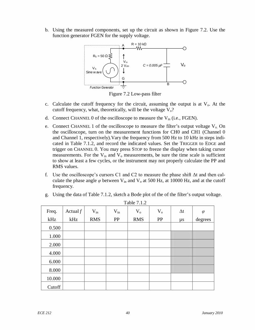
ECE 212 40 January 2010
b. Using the measured components, set up the circuit as shown in Figure 7.2. Use thefunction generator FGEN for the supply voltage.
Figure 7.2 Low-pass filter
c. Calculate the cutoff frequency for the circuit, assuming the output is at Vo. At thecutoff frequency, what, theoretically, will be the voltage Vo?
d. Connect CHANNEL 0 of the oscilloscope to measure the Vin (i.e., FGEN).
e. Connect CHANNEL 1 of the oscilloscope to measure the filter’s output voltage Vo. Onthe oscilloscope, turn on the measurement functions for CH0 and CH1 (Channel 0and Channel 1, respectively).Vary the frequency from 500 Hz to 10 kHz in steps indi-cated in Table 7.1.2, and record the indicated values. Set the TRIGGER to EDGE andtrigger on CHANNEL 0. You may press STOP to freeze the display when taking cursormeasurements. For the Vin and Vo measurements, be sure the time scale is sufficientto show at least a few cycles, or the instrument may not properly calculate the PP andRMS values.
f. Use the oscilloscope’s cursors C1 and C2 to measure the phase shift Δt and then cal-culate the phase angle φ between Vin and Vo at 500 Hz, at 10000 Hz, and at the cutofffrequency.
g. Using the data of Table 7.1.2, sketch a Bode plot of the of the filter’s output voltage.
Table 7.1.2
Freq.
kHz
Actual f
kHz
Vin
RMS
Vin
PP
Vo
RMS
Vo
PP
Δt
µs
φ
degrees
0.500
1.000
2.000
4.000
6.000
8.000
10.000
Cutoff
C = 0.005 µFVS
Sine w ave
R = 10 kΩ
RS = 50 Ω
Function Generator
A
G
B
V in
2 VPP Vo
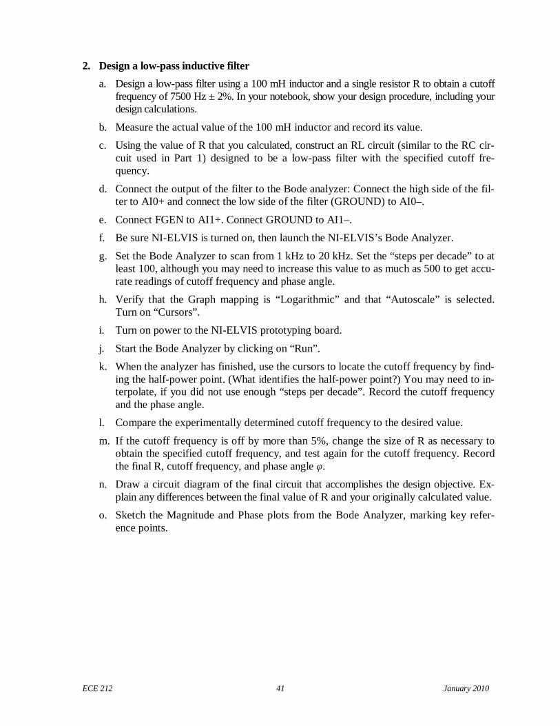
ECE 212 41 January 2010
2. Design a low-pass inductive filter
a. Design a low-pass filter using a 100 mH inductor and a single resistor R to obtain a cutofffrequency of 7500 Hz ± 2%. In your notebook, show your design procedure, including yourdesign calculations.
b. Measure the actual value of the 100 mH inductor and record its value.
c. Using the value of R that you calculated, construct an RL circuit (similar to the RC cir-cuit used in Part 1) designed to be a low-pass filter with the specified cutoff fre-quency.
d. Connect the output of the filter to the Bode analyzer: Connect the high side of the fil-ter to AI0+ and connect the low side of the filter (GROUND) to AI0–.
e. Connect FGEN to AI1+. Connect GROUND to AI1–.
f. Be sure NI-ELVIS is turned on, then launch the NI-ELVIS’s Bode Analyzer.
g. Set the Bode Analyzer to scan from 1 kHz to 20 kHz. Set the “steps per decade” to atleast 100, although you may need to increase this value to as much as 500 to get accu-rate readings of cutoff frequency and phase angle.
h. Verify that the Graph mapping is “Logarithmic” and that “Autoscale” is selected.Turn on “Cursors”.
i. Turn on power to the NI-ELVIS prototyping board.
j. Start the Bode Analyzer by clicking on “Run”.
k. When the analyzer has finished, use the cursors to locate the cutoff frequency by find-ing the half-power point. (What identifies the half-power point?) You may need to in-terpolate, if you did not use enough “steps per decade”. Record the cutoff frequencyand the phase angle.
l. Compare the experimentally determined cutoff frequency to the desired value.
m. If the cutoff frequency is off by more than 5%, change the size of R as necessary toobtain the specified cutoff frequency, and test again for the cutoff frequency. Recordthe final R, cutoff frequency, and phase angle φ.
n. Draw a circuit diagram of the final circuit that accomplishes the design objective. Ex-plain any differences between the final value of R and your originally calculated value.
o. Sketch the Magnitude and Phase plots from the Bode Analyzer, marking key refer-ence points.
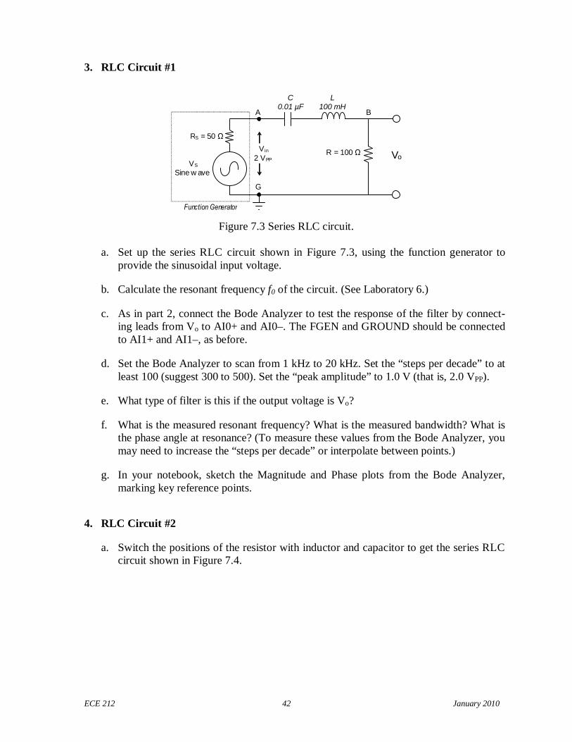
ECE 212 42 January 2010
3. RLC Circuit #1
Figure 7.3 Series RLC circuit.
a. Set up the series RLC circuit shown in Figure 7.3, using the function generator toprovide the sinusoidal input voltage.
b. Calculate the resonant frequency f0 of the circuit. (See Laboratory 6.)
c. As in part 2, connect the Bode Analyzer to test the response of the filter by connect-ing leads from Vo to AI0+ and AI0–. The FGEN and GROUND should be connectedto AI1+ and AI1–, as before.
d. Set the Bode Analyzer to scan from 1 kHz to 20 kHz. Set the “steps per decade” to atleast 100 (suggest 300 to 500). Set the “peak amplitude” to 1.0 V (that is, 2.0 VPP).
e. What type of filter is this if the output voltage is Vo?
f. What is the measured resonant frequency? What is the measured bandwidth? What isthe phase angle at resonance? (To measure these values from the Bode Analyzer, youmay need to increase the “steps per decade” or interpolate between points.)
g. In your notebook, sketch the Magnitude and Phase plots from the Bode Analyzer,marking key reference points.
4. RLC Circuit #2
a. Switch the positions of the resistor with inductor and capacitor to get the series RLCcircuit shown in Figure 7.4.
C0.01 µF
VS
Sine w ave
R = 100 Ω
RS = 50 Ω
Function Generator
A
G
B
V in
2 VPPVo
L100 mH
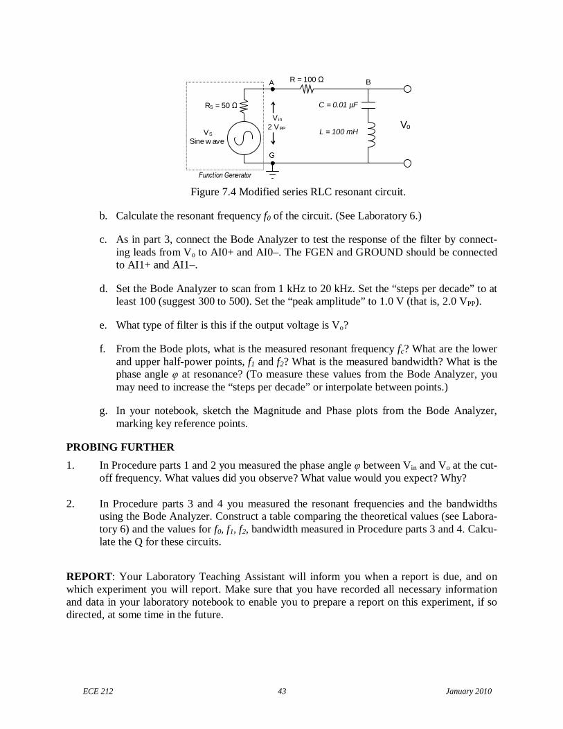
ECE 212 43 January 2010
Figure 7.4 Modified series RLC resonant circuit.
b. Calculate the resonant frequency f0 of the circuit. (See Laboratory 6.)
c. As in part 3, connect the Bode Analyzer to test the response of the filter by connect-ing leads from Vo to AI0+ and AI0–. The FGEN and GROUND should be connectedto AI1+ and AI1–.
d. Set the Bode Analyzer to scan from 1 kHz to 20 kHz. Set the “steps per decade” to atleast 100 (suggest 300 to 500). Set the “peak amplitude” to 1.0 V (that is, 2.0 VPP).
e. What type of filter is this if the output voltage is Vo?
f. From the Bode plots, what is the measured resonant frequency fc? What are the lowerand upper half-power points, f1 and f2? What is the measured bandwidth? What is thephase angle φ at resonance? (To measure these values from the Bode Analyzer, youmay need to increase the “steps per decade” or interpolate between points.)
g. In your notebook, sketch the Magnitude and Phase plots from the Bode Analyzer,marking key reference points.
PROBING FURTHER
1. In Procedure parts 1 and 2 you measured the phase angle φ between Vin and Vo at the cut-off frequency. What values did you observe? What value would you expect? Why?
2. In Procedure parts 3 and 4 you measured the resonant frequencies and the bandwidthsusing the Bode Analyzer. Construct a table comparing the theoretical values (see Labora-tory 6) and the values for f0, f1, f2, bandwidth measured in Procedure parts 3 and 4. Calcu-late the Q for these circuits.
REPORT: Your Laboratory Teaching Assistant will inform you when a report is due, and onwhich experiment you will report. Make sure that you have recorded all necessary informationand data in your laboratory notebook to enable you to prepare a report on this experiment, if sodirected, at some time in the future.
C = 0.01 µF
VS
Sine w ave
R = 100 Ω
RS = 50 Ω
Function Generator
A
G
B
V in
2 VPP VoL = 100 mH
ECE 212 44 January 2010
Laboratory 8
Transformers
INTRODUCTION: Transformers are magnetic circuit elements used in AC circuits for a varietyof applications. Transformers are often used to convert voltages from high to low values, orfrom low to high values. They are often used to isolate one AC line from another, for safetyor for equipment isolation. And they are often used to connect two components with mis-matched impedances, such as a high-impedance stereo amplifier and a low-impedancespeaker. This laboratory exercise will introduce transformer modeling concepts and explorethe characteristics of a common power transformer.
EDUCATIONAL OBJECTIVES: To teach the properties of common low-power transformers.
EXPERIMENTAL OBJECTIVES: To characterize the behavior of common power transform-ers, including concepts such as turns-ratios, impedance matching, and loading.
PRE-LAB:
Reading:
Review the sections of your ECE 262 textbook regarding transformer modeling.
Written:
In your laboratory notebook prepare for each circuit configuration (1) the circuit diagramyou will use and (2) a table in which you can record the values measured. See for exam-ple Tables 8.1, 8.2, and 8.3.
EQUIPMENT NEEDED:
Transformer Board with mounted 120V, center-tapped 12.6V transformer
NI-ELVIS II
Function generator
Oscilloscope, dual-beam
Digital Multimeter
Resistance Decade Substitution box
BACKGROUND
In its simplest form, a transformer consists of two closely coupled wire coils that share a com-mon magnetic field. If a voltage is applied to one of the coils (called the primary), then a voltagewill be induced on the second coil (called the secondary). The actual voltage induced in the sec-ondary coil is proportional to the ratio of the number of turns in the two coils. That ratio is calledthe turns ratio, for which we will use the symbol a. If the number of turns in the primary is N1
and the number of turns in the secondary is N2, the turns ratio a is
2
1
Na
N (8.1)

ECE 212 45 January 2010
and so,
2 2
1 1
N Va
N V and V2 = a · V1 . (8.2)
The two coils (also called windings) may be wound around air (an air core) or a dielectric, butmore often they are wound around a ferromagnetic material, such as steel (an iron core), in orderto concentrate the magnetic field and improve the coupling between the coils.
Transformers are most often used for three principal reasons: to change AC voltages; for electri-cal isolation; and for impedance matching.
Often we can assume that a transformer is "ideal", meaning that it has no internal power loss andall magnetic flux lines of the primary coil also pass through the secondary coil. The ideal modeloften fits large power transformers, where the losses are very small compared to the power trans-ferred. An ideal transformer delivers all of the applied power to the load. That is,
Power = I1V1 = I2V2 (8.3)
Rearranging this equation reveals an important relationship:
2 1 21 2 2
1 2 1
V I VI I I a or a
V I V . (8.4)
So, for example, if the secondary voltage is 1/10 the primary voltage, then the primary currentwill be 1/10 the secondary current. The equation further indicates that if there is no load current(I2=0), then the primary current is also zero.
Figure 8.1: Model for an ideal transformer
Impedance-MatchingBesides converting voltages, transformers are often used to match impedances between two elec-trical components, such as an audio amplifier (typically having 600Ω output impedance) and a speaker system (typically 4Ω or 8Ω impedance). The right transformer can make the load appear to have the same impedance as the source, and thereby maximize the power transferred to theload — and minimize the power lost in the source. The transformer that can perform such magi-cal matching will have the following property:
Zload~ V1 V2
+
–
+
–
I1 I2
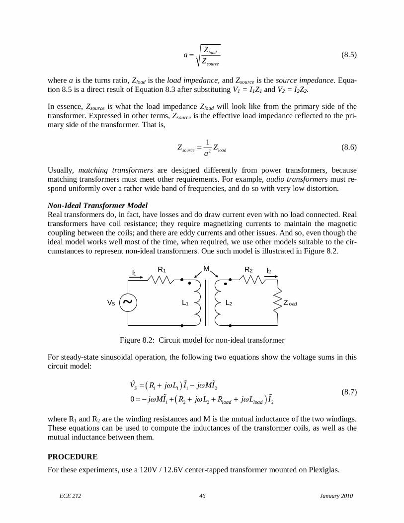
ECE 212 46 January 2010
load
source
Za
Z (8.5)
where a is the turns ratio, Zload is the load impedance, and Zsource is the source impedance. Equa-tion 8.5 is a direct result of Equation 8.3 after substituting V1 = I1Z1 and V2 = I2Z2.
In essence, Zsource is what the load impedance Zload will look like from the primary side of thetransformer. Expressed in other terms, Zsource is the effective load impedance reflected to the pri-mary side of the transformer. That is,
2
1source loadZ Z
a (8.6)
Usually, matching transformers are designed differently from power transformers, becausematching transformers must meet other requirements. For example, audio transformers must re-spond uniformly over a rather wide band of frequencies, and do so with very low distortion.
Non-Ideal Transformer ModelReal transformers do, in fact, have losses and do draw current even with no load connected. Realtransformers have coil resistance; they require magnetizing currents to maintain the magneticcoupling between the coils; and there are eddy currents and other issues. And so, even though theideal model works well most of the time, when required, we use other models suitable to the cir-cumstances to represent non-ideal transformers. One such model is illustrated in Figure 8.2.
Figure 8.2: Circuit model for non-ideal transformer
For steady-state sinusoidal operation, the following two equations show the voltage sums in thiscircuit model:
1 1 1 2
1 2 2 20
S
load load
V R j L I j MI
j MI R j L R j L I
(8.7)
where R1 and R2 are the winding resistances and M is the mutual inductance of the two windings.These equations can be used to compute the inductances of the transformer coils, as well as themutual inductance between them.
PROCEDURE
For these experiments, use a 120V / 12.6V center-tapped transformer mounted on Plexiglas.
Zload~ L1 L2
I1 I2R2R1
VS
M
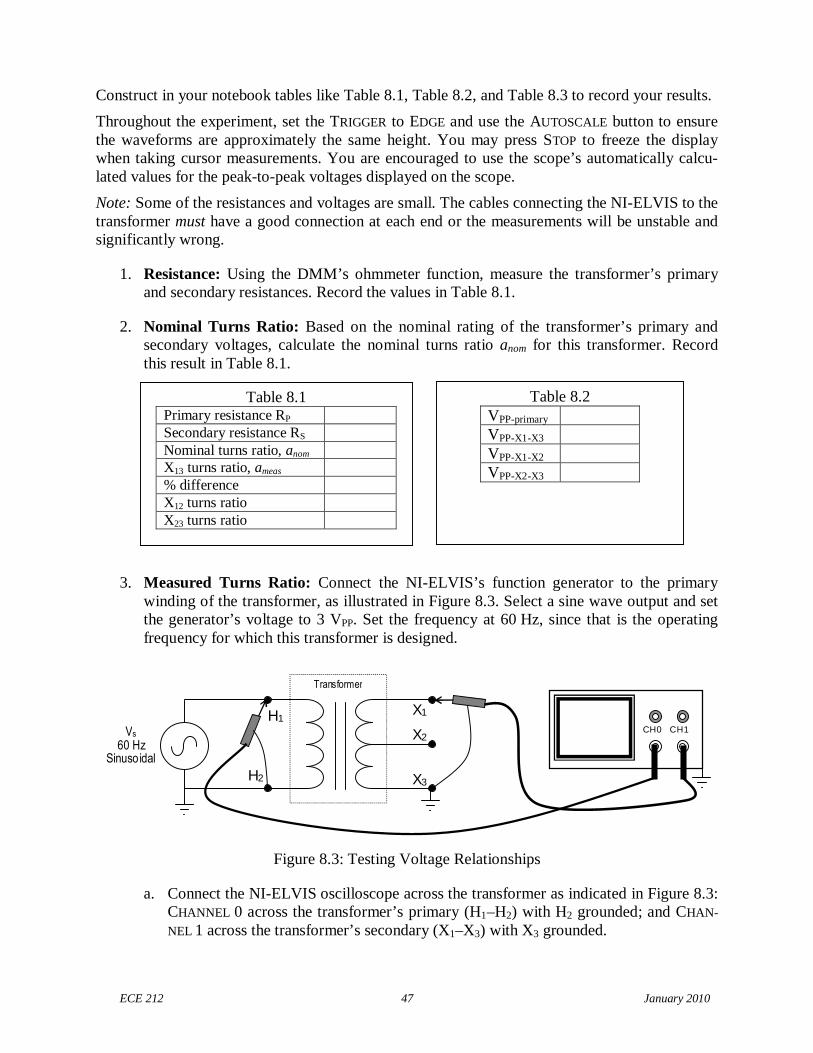
ECE 212
Construct in your notebook tables like Table 8.1, Table 8.2, and Table 8.3 to record your results.
Throughout the experiment, set the TRIGGER to EDGE and use the AUTOSCALE button to ensurethe waveforms are approximately the same height. You may press STOP to freeze the displaywhen taking cursor measurements. You are encouraged to use the scope’s automatically calcu-lated values for the peak-to-peak voltages displayed on the scope.
Note: Some of the resistances and voltages are small. The cables connecting the NI-ELVIS to thetransformer must have a good connection at each end or the measurements will be unstable andsignificantly wrong.
1. Resistance: Using the DMM’s ohmmeter function, measure the transformer’s primaryand secondary resistances. Record the values in Table 8.1.
2. Nominal Turns Ratio: Based on the nominal rating of the transformer’s primary andsecondary voltages, calculate the nominal turns ratio anom for this transformer. Recordthis result in Ta
3. Measured Tuwinding of thethe generator’sfrequency for w
a. Connect thCHANNEL 0NEL 1 acros
Vs
60 HzSinusoidal
Primary resisSecondary reNominal turnX13 turns rati% differenceX12 turns ratiX23 turns rati
Table 8.2VPP-primary
VPP-X1-X3
VPP-X1-X2
VPP-X2-X3
ble 8.1.
Table 8.1tance RP
sistance RS
s ratio, anom
o, ameas
o
47 January 2010
rns Ratio: Connect the NI-ELVIS’s function generator to the primarytransformer, as illustrated in Figure 8.3. Select a sine wave output and setvoltage to 3 VPP. Set the frequency at 60 Hz, since that is the operatinghich this transformer is designed.
Figure 8.3: Testing Voltage Relationships
e NI-ELVIS oscilloscope across the transformer as indicated in Figure 8.3:across the transformer’s primary (H1–H2) with H2 grounded; and CHAN-
s the transformer’s secondary (X1–X3) with X3 grounded.
Transformer
X1
X3
X2
H1
H2
CH0 CH1
o
ECE 212 48 January 2010
Use the oscilloscope to measure the transformer voltages indicated below and recordthe results in Table 8.2.
VPP across the primary (H1 to H2) (on CH0)
VPP across the secondary (X1 to X3) (on CH1, as illustrated in Figure 8.3)
VPP from the center tap (CT) to one side of the secondary (X1 to X2). (Move theCH1 ground lead to X2 to make the measurement.)
VPP from the center tap (CT) to the other side of the secondary (X2 to X3) (Movethe CH1 leads to X2 and X3 to make the measurement.)
b. Do you see why the connection X2 is referred to as the center tap?
c. Stop the function generator.
d. Calculate the turns ratio ameas between the primary winding and the secondary wind-ing X1–X3. Record the result in Table 8.1.
Calculate the % Difference between anom and ameas and record the result in Table 8.1:
% Difference 100%meas nom
nom
a a
a
Why are anom and ameas different? Based on your measurements, estimate what the ac-tual output voltage of the transformer (X1–X3) would be if the input voltage were120V.
e. Calculate the turns ratio ameas between the primary winding and the secondary wind-ing X1–X2. Record the result in Table 8.1.
f. Calculate the turns ratio ameas between the primary winding and the secondary wind-ing X2–X3. Record the result in Table 8.1.
4. Phase relationship between the primary and secondary voltages:
a. Connect the NI-ELVIS oscilloscope across the transformer, as indicated in Figure8.3: CHANNEL 0 across the transformer’s primary (H1–H2) with H2 grounded; andCHANNEL 1 across the transformer’s secondary (X1–X3) with X3 grounded.
b. Start the function generator (3 VPP at 60 Hz) and compare the phases of the twowaveforms. Are the voltages in phase or out of phase? In your notebook, sketch thewaveforms and record the phase shift, if any.
c. Reverse the scope leads on the secondary: that is, connect CHANNEL 1’s signal lead toX3 and the ground lead to X1. Describe the result and sketch the waveforms in yournotebook. Record the phase shift, if any.
d. Connect CHANNEL 1 of the scope to observe the secondary-side voltage from X2 (sig-nal) to X1 (ground). What is the difference from what you measured just previously inpart c?
e. Stop the function generator.
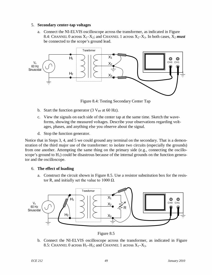
ECE 212 49 January 2010
5. Secondary center-tap voltages
a. Connect the NI-ELVIS oscilloscope across the transformer, as indicated in Figure8.4: CHANNEL 0 across X1–X2; and CHANNEL 1 across X2–X3. In both cases, X2 mustbe connected to the scope’s ground lead.
Figure 8.4: Testing Secondary Center Tap
b. Start the function generator (3 VPP at 60 Hz).
c. View the signals on each side of the center tap at the same time. Sketch the wave-forms, showing the measured voltages. Describe your observations regarding volt-ages, phases, and anything else you observe about the signal.
d. Stop the function generator.
Notice that in Steps 3, 4, and 5 we could ground any terminal on the secondary. That is a demon-stration of the third major use of the transformer: to isolate two circuits (especially the grounds)from one another. Attempting the same thing on the primary side (e.g., connecting the oscillo-scope’s ground to H1) could be disastrous because of the internal grounds on the function genera-tor and the oscilloscope.
6. The effect of loading
a. Construct the circuit shown in Figure 8.5. Use a resistor substitution box for the resis-tor R, and initially set the value to 1000 Ω.
Figure 8.5
b. Connect the NI-ELVIS oscilloscope across the transformer, as indicated in Figure8.5: CHANNEL 0 across H1–H2; and CHANNEL 1 across X1–X3.
Vs
60 HzSinusoidal
Transformer
X1
X3
X2
H1
H2
CH0 CH1
Vs
60 HzSinusoidal
Transformer
X1
X3
X2
H1
H2
CH0 CH1
R
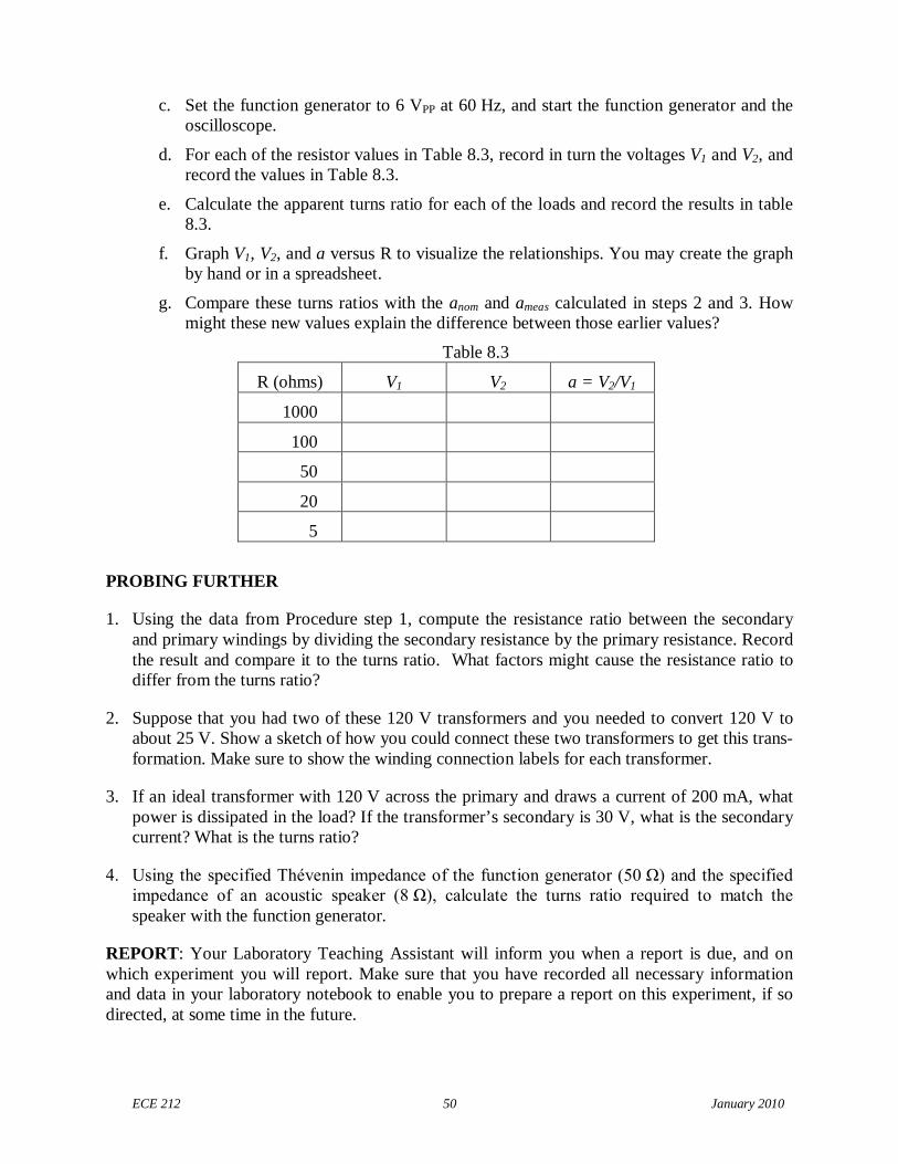
ECE 212 50 January 2010
c. Set the function generator to 6 VPP at 60 Hz, and start the function generator and theoscilloscope.
d. For each of the resistor values in Table 8.3, record in turn the voltages V1 and V2, andrecord the values in Table 8.3.
e. Calculate the apparent turns ratio for each of the loads and record the results in table8.3.
f. Graph V1, V2, and a versus R to visualize the relationships. You may create the graphby hand or in a spreadsheet.
g. Compare these turns ratios with the anom and ameas calculated in steps 2 and 3. Howmight these new values explain the difference between those earlier values?
Table 8.3
R (ohms) V1 V2 a = V2/V1
1000
100
50
20
5
PROBING FURTHER
1. Using the data from Procedure step 1, compute the resistance ratio between the secondaryand primary windings by dividing the secondary resistance by the primary resistance. Recordthe result and compare it to the turns ratio. What factors might cause the resistance ratio todiffer from the turns ratio?
2. Suppose that you had two of these 120 V transformers and you needed to convert 120 V toabout 25 V. Show a sketch of how you could connect these two transformers to get this trans-formation. Make sure to show the winding connection labels for each transformer.
3. If an ideal transformer with 120 V across the primary and draws a current of 200 mA, whatpower is dissipated in the load? If the transformer’s secondary is 30 V, what is the secondarycurrent? What is the turns ratio?
4. Using the specified Thévenin impedance of the function generator (50 Ω) and the specified impedance of an acoustic speaker (8 Ω), calculate the turns ratio required to match the speaker with the function generator.
REPORT: Your Laboratory Teaching Assistant will inform you when a report is due, and onwhich experiment you will report. Make sure that you have recorded all necessary informationand data in your laboratory notebook to enable you to prepare a report on this experiment, if sodirected, at some time in the future.
ECE 212 51 January 2010
Laboratory 9
Two-Port Network Characterization
INTRODUCTION: You have now had experience with transfer functions and the concept ofrelating output quantities to input quantities. Many circuits can be treated as modules wherean input is presented to two terminals (the "input port") and an output is taken from two ter-minals (the "output port"). Such circuits are termed two-port networks, and because they canbe treated as a unit — a block — they allow great simplification of large-scale designs.
The last chapter in your textbook is an introduction to two-port circuits and to the methodol-ogy for developing the sets of parameters that may be used to relate the output variables ofvoltage and current, typically designated as V2 and I2, respectively, to the input variables ofvoltage and current, typically designated as V1 and I1, respectively. This approach is used tocharacterize a variety of components and circuit element combinations from filters, throughtransistors, to microwave circuits.
EDUCATIONAL OBJECTIVE: The objectives of this laboratory exercise are to gain familiar-ity with three alternative two-port network parameter sets, to learn to measure the parametersets, and to demonstrate the operational definition of these parameters.
EXPERIMENTAL OBJECTIVE: To determine the impedance, admittance, and hybrid pa-rameter sets for an unknown two-port network.
PRE-LAB:
Reading:
Read the chapter in your textbook on two-port networks. Pay particular attention to theway in which the various parameters in each set (i.e., the z parameters, the y parameters,the h parameters, etc.) are defined.
Study the Background section below.
Written:
Review the steps in the procedure below and plan how you will make your measurementsto determine the required parameter values.
Sketch the test circuits you will use to make the measurements.
Construct suitable tables to record the measured values.
EQUIPMENT NEEDED:
NI-ELVIS II
Function generator
Oscilloscope, dual-beam
Digital Multimeter
Two-port Network Box
Resistor decade substitution box (1)
ECE 212 52 January 2010
BACKGROUND
A port consists of a pair of terminals; current enters through one of the terminals and the samecurrent leaves through the other terminal. A resistor is a one-port network. In this lab we willstudy two-port networks with one input port and one output port. Such networks are often treatedas “black boxes” or modules that may be plugged into a circuit to accomplish some task, such asfiltering the signal or providing a controlled voltage. Engineers need a way to characterize thebehavior of such a network and have developed several sets of parameters to do that. Each ofthese parameter sets relates the input (side 1) and output (side 2) voltages and currents.
In this lab we will use impedance, admittance, and hybrid parameter sets to characterize a simplecircuit. Impedance and admittance parameters are commonly used to characterize filters, and areoften useful in designing and characterizing impedance matching and power distribution net-works. The term immittance is often applied to the use of either impedance or admittance pa-rameters.
Be aware that because the voltages and currents are phasors with magnitude and phase angle, theparameters also have magnitude and phase angle. A simple RMS measurement will not suffice.
The impedance parameters (z parameters) relate the input and output voltages to the input andoutput currents by the following two equations:
1 11 1 12 2
2 21 1 22 2
V z I z I
V z I z I
(9.1)
or in matrix notation:
1 11 12 1
2 21 22 2
V z z I
V z z I
The z parameters have units of ohms and are most easily found by applying a set of open-circuittests on the circuit. When we apply a voltage to the input with the output open-circuited, we canmeasure the input current and output voltage and find the first two z parameters as follows:
2 2
1 211 21
1 10 0
;I I
V Vz z
I I
(9.2)
We can determine the other two z parameters by applying a similar test to the output with theinput open-circuited:
1 1
1 212 22
2 20 0
;I I
V Vz z
I I
(9.3)
Sometimes the impedance parameters do not exist because the voltages cannot be described byequation 9.1. Therefore, we need alternatives, such as the admittance parameters.
ECE 212 53 January 2010
The admittance parameters (y parameters) relate the input and output currents to the input andoutput voltages by the following two equations:
1 11 1 12 2
2 21 1 22 2
I y V y V
I y V y V
(9.4)
or in matrix notation:
1 11 12 1
2 21 22 2
I y y V
I y y V
The y parameters have units of siemens (or mhos) and are most easily found by applying a set ofshort-circuit tests on the circuit. When we apply a voltage to the inputs with the output short-circuited, we can measure the input current and output current to find the first two y parameters:
2 2
1 211 21
1 10 0
;V V
I Iy y
V V
(9.5)
We can determine the other two y parameters by applying a similar test to the output with theinput short-circuited:
1 1
1 212 22
2 20 0
;V V
I Iy y
V V
(9.6)
There are occasions where neither the impedance nor the admittance parameters exist, so there isneed for still another set of parameters.
The hybrid parameters (h parameters) are based on making V1 and I2 the dependent variables,and relating them to cross-variables V2 and I1.
. The h parameters satisfy the equations (9.7):
1 11 1 12 2
2 21 1 22 2
V h I h V
I h I h V
(9.7)
or in matrix notation:
1 11 12 1
2 21 22 2
V h h I
I h h V
The h parameters are found using a mix of short- and open-circuit tests as follows:
Short-circuit tests
2 2
1 211 21
1 10 0
;V V
V Ih h
I I
(9.8)

ECE 212 54 January 2010
Open-circuit tests
1 1
1 212 22
2 20 0
;I I
V Ih h
V V
(9.9)
PROCEDURE
Warning: Unless you are careful in your planning, in carrying out the experiment, and in re-cording your data, you are very likely to make errors. Here in this last laboratory you must figureout how to do most steps on your own.
Hint: Performing this lab is actually very straightforward, if you take it a step at a time. Thinkabout what you have learned during this semester. If you need to measure the phase angle of avoltage or current, you will need to use the oscilloscope. When necessary, insert a sense resistorof about 10 ohms and measure the voltage across it, including its phase shift, then calculate themagnitude of the current flowing through the sense resistor. Be sure that you have accuratelymeasured the resistor value, though, and not just relied on the nominal value. Use only one resis-tor decade box (it will make your life easier), and be careful where you put the resistor, so youdon’t make a grounding error on the oscilloscope. Carefully record each of the measurementsand calculations in tables that you have constructed for that purpose.
Think about what you are doing, sketch the circuits, work meticulously and methodically, andrecord your data carefully in tables.
1. Z parameters:
Use the function generator to apply a 1 kHz sine wave of about 10 VPP to the input termi-nals of the Two-port Network Box given to you by your instructor.
Make the current and voltage measurements necessary to calculate the parameters z11 andz21 for the z-parameter set. Note that you must determine not only the magnitude but alsothe phase of the voltages and currents involved. How can you do that with the instru-ments at hand?
Now apply the 10 VPP, 1 kHz sine wave to the output terminals.
Make the current and voltage measurements necessary to calculate the parameters Z12 andZ22.
Describe your procedure in your laboratory notebook and record the data necessary tocalculate the values for these parameters, including magnitude and phase.
2. Repeat Part 1 to determine the two-port parameter values for the y-parameter set.
3. Repeat Part 1, as needed, to determine the two-port parameter values for the h-parameterset.
PROBING FURTHER
1. Are the parameter values, which you have calculated for the various two-port network repre-sentations in this exercise valid for, say, 10 kHz? Why or why not?

ECE 212 55 January 2010
2. The z and y parameters should be related by a matrix inversion. Invert the 2x2 z parametermatrix and see if it matches with the y parameters you calculated in lab.
REPORT: Your Laboratory Teaching Assistant will inform you when a report is due, and onwhich experiment you will report. Make sure that you have recorded all necessary informationand data in your laboratory notebook to enable you to prepare a report on this experiment, if sodirected, at some time in the future.
ECE 212 56 January 2010
Laboratory 10
Final Exam
INTRODUCTION: This has been your second engineering circuits laboratory. Although youhave been provided with a "cookbook" (this manual), hopefully you have not just blindly fol-lowed the instructions in order to get a good grade. If you have, you have cheated only your-self. The theory, which you have learned from your textbook and lectures, is a way of look-ing at reality and thinking about how to organize experience, i.e. dealing with real, physicalthings. It is only through combining practical experience with theory that you can begin todevelop the necessary analytical skills to aid you in "taking things apart and putting them to-gether in new ways" that is the essence of the practice of engineering.
EDUCATIONAL OBJECTIVE: This examination is designed to help you and your LTA de-termine how much you have developed your knowledge, skills, and self confidence.
PRE-LAB: Review your lab manual. Think carefully of the procedures that you have followedand what you have learned from them. How do you measure voltage, current, resistance, fre-quency, etc.? How accurate are your measurements? How are your measurements affected bythe frequency response of your measuring instruments? Can you develop linear, semi-log, orlog-log plots of your data to facilitate interpretation?
EQUIPMENT NEEDED:
PencilCalculator
PROCEDURE
The final exam will consist of a written exam and a practical exam. The practical exam involvesperforming a lab procedure to obtain a desired result. The written exam will cover the applicationof theory to understand circuit behavior, based upon your laboratory experiences in this course.
PROBING FURTHER
This has been the second in a series of four (4) laboratory courses. Regardless of the LTA whomay teach your next course - what have you done to develop your expertise and skills? What willyou do differently in the next course? What have you learned from your experience?
ECE 212 57 January 2010
Appendix A
Safety
Electricity, when improperly used, is very dangerous to people and to equipment. This is espe-cially true:
in industrial environments, where large amounts of power are available, and high volt-ages are present;
in environments where people are especially susceptible to electric shock, for example,where high-voltage systems must be maintained while in operation, or in hospitals whereelectronic equipment is used to test or control physiological functions; and
in experimental or teaching laboratory environments, where inexperienced personnel mayuse electrical equipment in experimental or nonstandard configurations.
Engineers play a vital role in eliminating or alleviating the danger in all three environments.Where standard equipment is used in standard configurations, governmental agencies and insur-ance underwriters impose strict laws and regulations on the operation and use of electricalequipment, including switchgear, power lines, safety devices, etc. As a result, corporations andother organizations in turn impose strict rules and methods of operation on their employees andcontractors. Engineers who are involved in using electrical equipment, in supervising others whouse it, and in designing such systems, have a great responsibility to learn safety rules and prac-tices, to observe them, and to see that a safe environment is maintained for those they supervise.In any working environment there is always pressure to “get the job done” and take short cuts.The engineer, as one who is capable of recognizing hazardous conditions, is in a responsible po-sition both as an engineer and as a supervisor or manager and must maintain conditions to protectpersonnel and avoid damage to equipment.
Because of their non-standard activities, experimental laboratories are exempt from many ofthese rules and regulations. This puts more responsibility on the engineer in this environment toknow and enforce the safest working procedures.
The learning necessary to develop the knowledge, the habit-forming experience to work safelyaround electrical equipment, and the ability to design safe electrical equipment begins with thefirst student laboratory experience and continues throughout life. This includes learning the typesof electrical injuries and damage, the physiology of electrical injuries, ways to prevent such inju-ries, and steps to take when accidents occur.
Physiology of Electrical Injuries
Four main types of electrical injuries include the following: electric shock; electrical burns; injuries resulting from falls caused by electric shock; “sunburned” eyes from looking at a bright electric arc, such as that of an arc-welder.
While this is very painful and may cause loss of work time, it is usually temporary.
ECE 212 58 January 2010
Other injuries may be indirectly caused by electrical accidents, such as burns from exploding oil-immersed switchgear or transformers.
Although electric shock is normally associated with contact with high-voltage alternating current(AC), under some circumstances death can occur from voltages substantially less than the nomi-nal 120 volts AC found in residential systems. Electric shock is caused by an electric currentpassing through a part of the body. The human body normally has a high resistance to electriccurrents, so a high voltage is usually required to cause lethal currents. This resistance is almostall at the skin, however, and when the skin is wet its resistance is much lower. When a person ishot and sweaty or is standing in water, contact with 120 volts or less may well cause a fatalshock.
Electric shock is not a single phenomenon but is a disturbance of the nerves by an electric cur-rent. A current through a part of the body such as the arm or leg will cause pain and muscle con-traction. If a victim receives an electric shock from grasping a live conductor, a current of greaterthan 15 to 30 milliamperes through the arm will cause muscle contractions so severe that the vic-tim cannot let go. Similar currents through leg muscles may cause sudden contractions that makethe victim jump or fall, possibly resulting in further injuries or death. Prolonged contact of morethan a minute or so may cause chest muscles to contract, preventing breathing and resulting insuffocation or brain damage from lack of oxygen.
Death by electric shock is most often attributed to ventricular fibrillation, which is an uncon-trolled twitching or beating of the heart that produces no pumping action and therefore no bloodcirculation. Unless corrective action is taken, death follows quickly from lack of oxygen to thebrain. While the amount of current that will cause fibrillation depends on several variables, 0.5 to5 amperes through the body will normally cause the very small current (approximately 1 mA)through the heart that is sufficient to cause fibrillation in most people. Larger currents than thisthrough the heart cause contraction or clamping of the heart muscle, resulting in death unlesscorrective action is taken.
Electric burns may be caused by electric currents flowing in or near parts of the body. Such bumsare similar to bums from ordinary heat sources, except that those caused by high-frequency cur-rents are generally deeper and take longer to heal the other bums. Electrocution will often leavesevere burns at the points where the current entered and left the body.
Source of Electric Shock
Since electric shock is caused by an electric current flowing through a part of the body, the prob-lem may be prevented by not allowing the body to become part of any electric circuit. For thisreason, one needs to understand how a person might inadvertently become part of an electric cir-cuit, and the most likely way is through accidental grounding.
Electric circuits may be classified as either grounded or ungrounded. Grounded circuits are saferfor most conditions, since the voltages at all points in the circuit are known and it is easier to pro-tect against fault conditions. The disadvantage of a grounded circuit is that a person standing ona non-insulated floor can receive a shock by touching only one conductor.
ECE 212 59 January 2010
Almost all electric power generation, transmission, and distribution systems are grounded to pro-tect people and equipment against fault conditions caused by windstorms, lightning, etc. Resi-dential, commercial, and industrial systems, such as lighting and heating, are always groundedfor greater safety. Communication and computer systems, as well as general electronic equip-ment (e.g., DC power supplies, oscilloscopes, oscillators, and digital multimeters) are groundedfor safety and to prevent or reduce electrical noise, crosstalk, and static.
Ungrounded circuits are used in systems where isolation from other systems is necessary, wherelow voltages and low power are used, and where obtaining a suitable ground connection is diffi-cult or impractical. In an ungrounded circuit, contact with two points in the circuit that are at dif-ferent potentials is required to produce a shock. The hazard is that, with no specific ground insuch circuits, a hidden fault can cause some random point to be grounded, in which case, touch-ing a supposedly safe conductor while standing on the ground could result in an electric shock.
Protecting People and Equipment in the Laboratory
Strict adherence to several common-sense rules, summarized below, can prevent electric shockto individuals and damage to laboratory equipment.
Protecting People
1. When building a circuit, connect the power source last, while the power is OFF.
2. Before changing a circuit, turn off or disconnect the power if possible.
3. Never work alone where the potential of electric shock exists.
4. When changing an energized connection, use only one hand. A common practice is to putone hand behind your back when touching a circuit that is possibly energized. Nevertouch two points in a circuit that are at different potentials.
5. Know and check that the circuit and connections are correct before applying power.
6. Avoid touching capacitors that may have a residual charge. Stored energy in a capacitorcan cause severe shock even after a long period of time.
7. Insulate yourself from ground by standing on insulating mats where appropriate.
The above rules and the additional rules given below also serve to protect instruments and othercircuits from damage.
Protecting Equipment
1. Set the scales of measurement instrument to the highest range before applying power.
2. When using an oscilloscope, do not leave a bright spot or trace on the screen for long pe-riods of time. Doing so can burn the image into the screen.
3. Be sure instrument grounds are connected properly. Avoid ground loops and accidentalgrounding of “hot” leads.
4. Check polarity markings and connections of instruments carefully before connectingpower.
5. Never connect an ammeter across a voltage source, but only in series with a load.
ECE 212 60 January 2010
6. Do not exceed the voltage or current ratings of circuit elements or instruments. This par-ticularly applies to wattmeters, since the current or voltage rating may be exceeded withthe needle still reading on the scale.
7. Be sure any fuses and circuit breakers are of suitable value.
When connecting electrical elements to make up a network in the laboratory, it easy to lose trackof various points in the network and accidentally connect a wire to the wrong place. One proce-dure to help avoid this problem is to connect first the main series loop of the circuit, then go backand add the elements in parallel.
Types of Equipment Damage
Excessive currents and voltages can damage instruments and other circuit elements. A largeover-current for a short time or a smaller over-current for a longer time will cause overheating,resulting in insulation scorching and equipment failure.
Blown fuses are the most common equipment failure mode in this laboratory. The principalcauses for these failures include:
incorrectly wired circuits; accidental shorts; switching resistance settings while power is applied to the circuit; changing the circuit while power is applied; using the wrong scale on a meter; connecting an ammeter across a voltage source; using a low-power resistor box (limit ½ amp) when high power is required; turning on an autotransformer at too high a setting.
All of these causes are the result of carelessness by the experimenter.
Some type of insulating material, such as paper, cloth, plastic, or ceramic, separates conductorsthat are at different potentials in electrical devices. The voltage difference that this material canwithstand is determined by design (type, thickness, moisture content, temperature, etc.). Exceed-ing the voltage rating of a device by an appreciable amount can cause arcing or corona, resultinginsulation breakdown, and failure.
Some electrical devices can also be damaged mechanically by excessive currents. An example isthe D’Arsonval meter, the indicator in most analog metering instruments. A large pulse of over-current will provide mechanical torque that can cause the needle to wrap around the pin at thetop of the scale, thereby causing permanent damage even though the current may not have beenon long enough to cause failure due to overheating.
After-Accident Action
Since accidents do happen despite efforts to prevent them, preparation for an accident can savevaluable time and lives. This preparation should include immediate availability of first aid mate-rial suitable for minor injuries or for injuries that are likely because of the nature of the work.
ECE 212 61 January 2010
Knowledge of how to obtain trained assistance such as Emergency Medical Service (EMS)should be readily available for everyone.
Treating victims for electrical shock includes four basic steps, shown below, that should be takenimmediately. Step two requires qualification in CPR and step three requires knowledge ofmouth-to-mouth resuscitation. Everyone who works around voltages that can cause dangerouselectrical shock should take advantage of the many opportunities available to become qualifiedin CPR and artificial respiration.
Immediate Steps After Electric Shock
1. Shut off all power and remove victim from the electric circuit. If the power cannot be shut offimmediately, use an insulator of some sort, such as a wooden pole, to remove the victim fromthe circuit. Attempts to pull the victim from the circuit with your hands will almost alwaysresult in your joining the victim in electric shock.
2. If you are qualified in CPR, check for ventricular fibrillation or cardiac arrest. If either is de-tected, external cardiac massage should be started at once. Whether you are qualified in CPRor not, notify the EMS and the ECE Department at once, using the telephone numbers listedbelow.
3. Check for respiratory failure and take appropriate action. This may have resulted from physi-cal paralysis of respiratory muscles or from a head injury. Sometimes many hours pass be-fore normal respiration returns. Artificial respiration should be continued until trained EMSassistance arrives.
4. Check for and treat other injuries such as fractures from a fall or burns from the current’s en-try and exit sites.
Investigations are always made after accidents. As an engineer, you will be involved as a part ofthe investigating team or in providing information to an investigator. Information obtained andnotes written immediately after the emergency will aid the investigation and assist in preventingfuture accidents of a similar nature.
EMERGENCY NUMBERS
All Emergencies 911Student Health Center 656-2233ECE Department Office 656-5650Clemson Police 656-2222
References
1. W. F. Cooper, Electrical Safety Engineering. Newnes-Butterworth, London-Boston, 1978.
2. W. H. Buchsbaum and B. Goldsmith, Electrical Safety in the Hospital, Medical EconomicsCompany, Oradell, NJ, 1975.
3. J. G. Webster, Editor, Medical Instrumentation Application and Design. Houghton MifflinCompany, Boston, 1978.
ECE 212 62 January 2010
Appendix B
Instruments for Electrical Measurements
Electrical engineers measure and use a wide variety of electrical circuit variables, such as volt-age, current, frequency, power, and energy, as well as electrical circuit parameters, such as resis-tance, capacitance, and inductance. Many instruments can be used to make such measurements,but the proper use of the instruments and interpretation of the measurements depend on a funda-mental understanding of how the instruments work, their capabilities, and their limitations.
This appendix provides a brief overview of the fundamentals of the electrical equipment and in-struments that you will use in this and other laboratory courses. As you encounter more and var-ied types of electrical equipment and instruments in this and subsequent courses, you will findseveral books, in addition to your textbook, useful in developing your understanding and meas-urement skills. In addition, many commercial instrument manufacturers publish handbooks andapplication notes that provide more information on specific measurement techniques.
Measurement of Current and Voltage
The basic electrical circuit variables of current and voltage are measured with ammeters (for cur-rent) and voltmeters (for voltage). These instruments may use either analog (continuous) or digi-tal (numerical) indicators (“readouts”) to report the measurement results.
Basic facts you should keep in mind include the following:
An ammeter is a low resistance instrument to measure current. It is inserted in serieswith the with circuit branch of interest. If connected in parallel with a component, it willlikely short out the component and blow the fuse or burn out the circuit or the instrument.
A voltmeter is a high resistance instrument for measuring voltage. It is connected inparallel with the component(s) of interest. Voltage is also called “electromotive force” orEMF.
Analog Meter Instruments
Analog meter instruments were developed early in the history of electrical science and technol-ogy. Most are based on the d’Arsonval galvanometer movement. A brief description of this me-ter movement and its use in ammeters and voltmeters is given in the textbook Electric Circuitsby J. W. Nilsson and S.A. Riedel [B-1], on pages 78 through 80 in the Seventh Edition. Moreinformation is available in Reference B-2.
In the d’Arsonval galvanometer, current through a coil of fine wire develops a magnetic fieldthat opposes the field of a permanent magnet, and so rotates a needle across a scale that ismarked off in units of the measured variable. This type of movement is used extensively in DCanalog instruments. For AC measurement, however, the d’Arsonval movement is not sufficientby itself, but must be adapted in some way:
ECE 212 63 January 2010
it must be used in conjunction with a rectifier diode that converts the AC into a waveformwith a DC level to which the meter can respond, or
it must use an electromagnet instead of the permanent magnet in the standard d’Arsonvalmovement, or
it must use iron vanes [B-3].
Figure B.1 (a) shows an equivalent circuit representation of a dual-coil electrodynamometerwattmeter often used to measure 60 Hz AC power. It employs the electromagnet form of thegalvanometer. Because the meter deflection is proportional to the product of the current throughthe current-sensing coil (in series with the load) and the current through the voltage sensing coil(across the load), the response is proportional to the product of the load current and the load volt-age drop. The size of the resistance in series with the voltage coil determines the voltage range ofthe instrument.
Figure B.1 (b) shows the equivalent circuit representation of the analog voltmeter. The size ofthe resistor determines the voltmeter range.
Figure B.1 (c) shows the equivalent circuit of the analog ammeter. The size of the shunt (paral-lel) resistor determines the range of the ammeter.
Note that analog instruments often have non-linear scales.
(a) (b) (c)
Figure B.1: (a) Equivalent circuit for analog wattmeter. (b) Equivalent circuitfor analog voltmeter. (c) Equivalent circuit for analog ammeter.
Digital Multimeter
A multimeter is an electronic device that measures a multitude of electrical values, usually in-cluding at least AC and DC voltage and current, as well as resistance. Analog multimeters havean analog display and digital multimeter (DMM) have a digital display. The DMM in this labora-tory is part of the NI-ELVIS II and is used to measure voltage (DC and AC), current (DC andAC), resistance, capacitance, inductance. Additionally it may be used for diode tests and audiblecontinuity tests. For capacitance and inductance measurements you must make connections to
ECE 212 64 January 2010
the DMM/Impedance Analyzer on the prototyping board. For all other measurements make con-nections to the DMM banana jacks on the workstation.
The primary DMM instrument on NI ELVIS II Series is isolated and its terminals are the threebanana jacks on the side of the workstation. For DC Voltage, AC Voltage, Resistance, Diode,and Continuity Test modes, use the VΩ and COM connectors. For DC Current and AC Current modes, use the A and COM connectors. For easy access to circuits on the prototyping board, youcan use banana-to-banana cables to wrap the signals from the user-configurable banana jacks tothe DMM connectors on the workstation. For capacitance and inductance tests, the positive endof the device under test is connected to the pin “DUT+” on the prototyping board, and the nega-tive end of the device under test should be connected to the pin “DUT–” on the prototypingboard.
For details about the DMM and other NI-ELVIS instruments, refer to the ELVIS Operation Man-ual at http://www.clemson.edu/ces/departments/ece/resources/lab_manuals.html.
(a) (b)
Figure B.11 (a) Equivalent circuit for voltage and current measurement with the DMM.(b) Equivalent circuit for resistance measurement with the DMM.
Dual-Beam Oscilloscope
The oscilloscope is a tool to allow engineers to look at the shape of an electrical voltage versustime or versus a second signal. Until relatively recently, oscilloscopes used a cathode ray tube(CRT) to draw the waveforms onto a screen, just like an image on a television. Televisions andcomputer monitors also used cathode ray tubes until the advent of the new flat screens. Most en-gineers refer to the instrument as a “scope”.
The Dual-Beam Oscilloscope has two vertical (“y”) input channels and one horizontal (“x”)channel. The horizontal channel can be connected either to an external AC voltage signal or to aninternal time-base generator (x = time). You should become familiar with the scale options onthe y input channels, the x input channel, and the time base, since you will be using these to ob-tain values for voltage and time. The y inputs can be either direct (1X) or through a 10X probe.Figure B.12 (a) shows the equivalent input circuit for a direct input and Figure B.12 (b) shows anequivalent circuit for the 10X probe input. Note that in both configurations one side of the inputis grounded, which means that care must be used in connecting the ground clip of the probe or
ECE 212 65 January 2010
connector used to assure that these are not connected to a “hot” (|V| > 0) part of the circuit. (Seethe section “Oscilloscope Grounding Errors”.) The calibrated time base is useful when measur-ing the phase difference between two waveforms (on the y1 and y2 inputs) by carefully lining upthe zero levels for both y inputs and then using in the ac-couple mode to observe the time differ-ence between zero crossings of the two waveforms.
20 pF
Figure B.12: (a) Equivalent circuit for oscilloscope input with 1X probe (direct input).(b) Equivalent circuit for oscilloscope input with 10X probe.
Digital Storage Oscilloscope
The digital storage oscilloscope (DSO) is now the preferred type of oscilloscope for most indus-trial applications, although analog oscilloscopes are still widely used. The DSO uses digitalmemory to store data as long as required without degradation. The digital storage allows use ofan enormous array of sophisticated digital signal processing tools for the analysis of complexwaveforms in today’s circuitry.
The digital storage oscilloscopes of the NI-ELVIS are dual-beam oscilloscopes with two verticalinputs, as described above. The vertical input on the oscilloscope, instead of driving a verticalamplifier, is digitized by an analog-to-digital (A-to-D) converter to create a data set that is storedin the memory of a microprocessor. The data set is processed and then sent to the display. Thedata set can be written to a flash drive or sent over a LAN or a WAN for processing or archiving.The screen image can be directly recorded on paper by means of an attached printer or plotter,without the need for an oscilloscope camera. The scope’s own signal analysis software can ex-tract many useful time-domain features (e.g. rise time, pulse width, amplitude), frequency spec-tra, histograms and statistics, persistence maps, and a large number of parameters meaningful toengineers in specialized fields such as telecommunications, disk drive analysis, and power elec-tronics.
Digital oscilloscopes are limited principally by the performance of the analog input circuitry andthe sampling frequency. In general, the sampling frequency should be at least the Nyquist rate –double the frequency of the highest-frequency component of the observed signal – to avoid alias-ing.
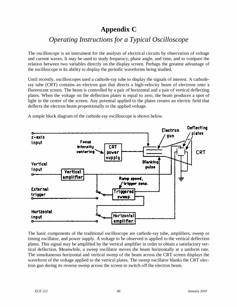
ECE 212 66 January 2010
Appendix C
Operating Instructions for a Typical Oscilloscope
The oscilloscope is an instrument for the analysis of electrical circuits by observation of voltageand current waves. It may be used to study frequency, phase angle, and time, and to compare therelation between two variables directly on the display screen. Perhaps the greatest advantage ofthe oscilloscope is its ability to display the periodic waveforms being studied.
Until recently, oscilloscopes used a cathode-ray tube to display the signals of interest. A cathode-ray tube (CRT) contains an electron gun that directs a high-velocity beam of electrons onto afluorescent screen. The beam is controlled by a pair of horizontal and a pair of vertical deflectingplates. When the voltage on the deflection plates is equal to zero, the beam produces a spot oflight in the center of the screen. Any potential applied to the plates creates an electric field thatdeflects the electron beam proportionally to the applied voltage.
A simple block diagram of the cathode-ray oscilloscope is shown below.
The basic components of the traditional oscilloscope are cathode-ray tube, amplifiers, sweep ortiming oscillator, and power supply. A voltage to be observed is applied to the vertical deflectionplates. This signal may be amplified by the vertical amplifier in order to obtain a satisfactory ver-tical deflection. Meanwhile, a sweep oscillator moves the beam horizontally at a uniform rate.The simultaneous horizontal and vertical sweep of the beam across the CRT screen displays thewaveform of the voltage applied to the vertical plates. The sweep oscillator blanks the CRT elec-tron gun during its reverse sweep across the screen to switch off the electron beam.
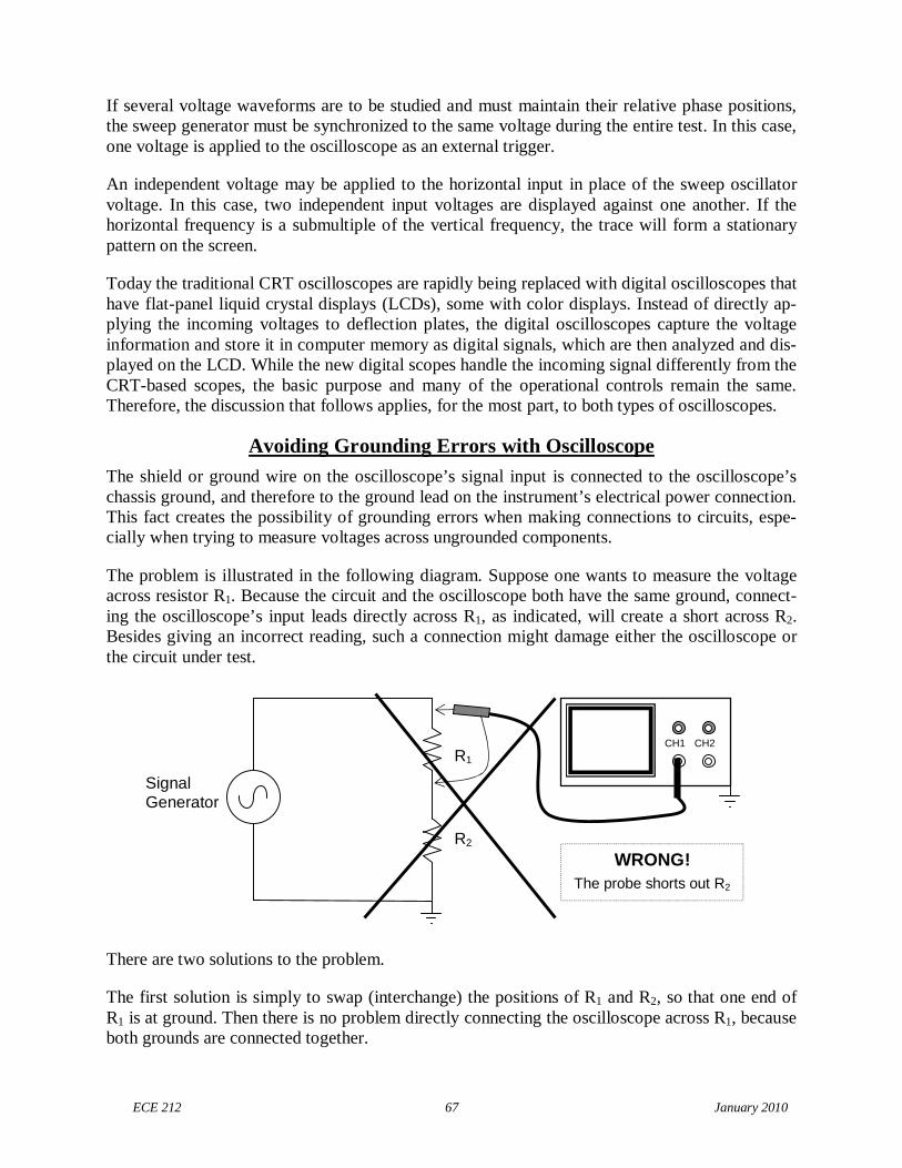
ECE 212 67 January 2010
If several voltage waveforms are to be studied and must maintain their relative phase positions,the sweep generator must be synchronized to the same voltage during the entire test. In this case,one voltage is applied to the oscilloscope as an external trigger.
An independent voltage may be applied to the horizontal input in place of the sweep oscillatorvoltage. In this case, two independent input voltages are displayed against one another. If thehorizontal frequency is a submultiple of the vertical frequency, the trace will form a stationarypattern on the screen.
Today the traditional CRT oscilloscopes are rapidly being replaced with digital oscilloscopes thathave flat-panel liquid crystal displays (LCDs), some with color displays. Instead of directly ap-plying the incoming voltages to deflection plates, the digital oscilloscopes capture the voltageinformation and store it in computer memory as digital signals, which are then analyzed and dis-played on the LCD. While the new digital scopes handle the incoming signal differently from theCRT-based scopes, the basic purpose and many of the operational controls remain the same.Therefore, the discussion that follows applies, for the most part, to both types of oscilloscopes.
Avoiding Grounding Errors with Oscilloscope
The shield or ground wire on the oscilloscope’s signal input is connected to the oscilloscope’schassis ground, and therefore to the ground lead on the instrument’s electrical power connection.This fact creates the possibility of grounding errors when making connections to circuits, espe-cially when trying to measure voltages across ungrounded components.
The problem is illustrated in the following diagram. Suppose one wants to measure the voltageacross resistor R1. Because the circuit and the oscilloscope both have the same ground, connect-ing the oscilloscope’s input leads directly across R1, as indicated, will create a short across R2.Besides giving an incorrect reading, such a connection might damage either the oscilloscope orthe circuit under test.
There are two solutions to the problem.
The first solution is simply to swap (interchange) the positions of R1 and R2, so that one end ofR1 is at ground. Then there is no problem directly connecting the oscilloscope across R1, becauseboth grounds are connected together.
SignalGenerator
R1
R2
CH1 CH2
WRONG!
The probe shorts out R2
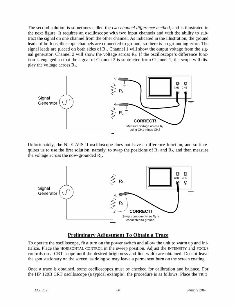
ECE 212 68 January 2010
The second solution is sometimes called the two-channel difference method, and is illustrated inthe next figure. It requires an oscilloscope with two input channels and with the ability to sub-tract the signal on one channel from the other channel. As indicated in the illustration, the groundleads of both oscilloscope channels are connected to ground, so there is no grounding error. Thesignal leads are placed on both sides of R1. Channel 1 will show the output voltage from the sig-nal generator. Channel 2 will show the voltage across R2. If the oscilloscope’s difference func-tion is engaged so that the signal of Channel 2 is subtracted from Channel 1, the scope will dis-play the voltage across R1.
Unfortunately, the NI-ELVIS II oscilloscope does not have a difference function, and so it re-quires us to use the first solution; namely, to swap the positions of R1 and R2, and then measurethe voltage across the now-grounded R1.
Preliminary Adjustment To Obtain a Trace
To operate the oscilloscope, first turn on the power switch and allow the unit to warm up and ini-tialize. Place the HORIZONTAL CONTROL in the sweep position. Adjust the INTENSITY and FOCUS
controls on a CRT scope until the desired brightness and line width are obtained. Do not leavethe spot stationary on the screen, as doing so may leave a permanent burn on the screen coating.
Once a trace is obtained, some oscilloscopes must be checked for calibration and balance. Forthe HP 120B CRT oscilloscope (a typical example), the procedure is as follows: Place the TRIG-
SignalGenerator
R2
R1
CH1 CH2
CORRECT!Swap components so R1 is
connected to ground.
SignalGenerator
R1
R2
CH1 CH2
CORRECT!Measure voltage across R1
using CH1 minus CH2

ECE 212 69 January 2010
GER LEVEL on AUTO and the TRIGGER SOURCE to INT. Turn the horizontal and vertical VERNIERS toCAL, the VERTICAL SENSITIVITY to CAL, and the HORIZONTAL DISPLAY to 1 msec/cm. With thecontrols in these positions, an internal calibrating signal is produced on the screen. Turn the CAL
adjustment until the upper and lower peaks of the square wave are 6 cm apart.
Digital oscilloscopes often have automated setup and calibration upon power-up.
Waveform Observation
After the initial adjustments are made, the oscilloscope is ready for operation. To observe thewaveform of any periodic signal, apply the signal to the vertical input terminals. Use DC cou-pling if the input is DC or very low in frequency or if you want to capture any DC offset. Nowthe signal from an oscillator, signal generator, or some component of an electrical circuit may beobserved on the screen. The best resolution of the waveform is obtained when the time scale isadjusted so one or two cycles appear on the screen and when the vertical scale is adjusted so theamplitude occupies most of the graticule. If the waveform will not stabilize, adjust the SYNC orTRIGGER just enough to cause the pattern to stop. Whenever possible, connect the oscilloscopeground to the common ground of the circuit. Exercise great care when making measurementswith both terminals above ground potential, as there may be a difference in potential betweentwo instrument cases, causing ground loop currents, faulty readings, and damaged equipment.
Voltage Measurement (AC & DC)
The oscilloscope has advantages as a voltmeter: a very high input impedance compared to ananalog voltmeter;, the ability to measure voltages over a very wide frequency range; and the abil-ity to indicate magnitude regardless of waveform. Also, scopes measure peak-to-peak values ofAC voltages, whereas standard AC voltmeters measure rms values of sine wave voltages. How-ever, the oscilloscope only has an accuracy of 2% to 5%, while the AC voltmeter’s accuracy willbe from 0.25% to 2%.
To use the oscilloscope as an AC voltmeter, apply the signal to the vertical input terminals, andadjust the calibrated VERTICAL SENSITIVITY (or VOLTS/DIV) so the amplitude is of suitable magni-tude on the graticule. Thepeak-to-peak value is then thedistance indicated multipliedby the vertical calibration. Forexample, assume that a sinewave generator is set to 1000Hz and adjusted for maximumoutput voltage. A peak-to-peakvalue of 60V is observed onthe oscilloscope. The output ofthe generator at 1000 Hz,therefore, is approximately60V peak-to-peak, and 21.2Vrms.
Note:1
2 2rms p pV V
r ms value= 21.2 V
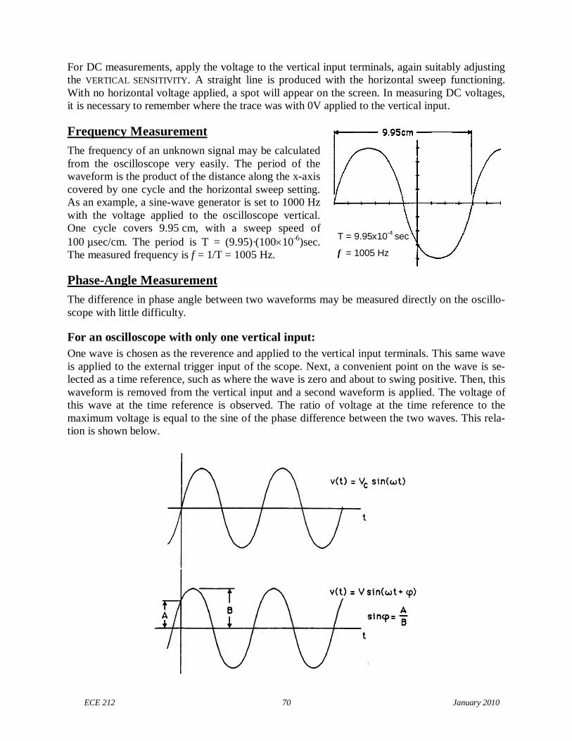
ECE 212 70 January 2010
For DC measurements, apply the voltage to the vertical input terminals, again suitably adjustingthe VERTICAL SENSITIVITY. A straight line is produced with the horizontal sweep functioning.With no horizontal voltage applied, a spot will appear on the screen. In measuring DC voltages,it is necessary to remember where the trace was with 0V applied to the vertical input.
Frequency Measurement
The frequency of an unknown signal may be calculatedfrom the oscilloscope very easily. The period of thewaveform is the product of the distance along the x-axiscovered by one cycle and the horizontal sweep setting.As an example, a sine-wave generator is set to 1000 Hzwith the voltage applied to the oscilloscope vertical.One cycle covers 9.95 cm, with a sweep speed of100 µsec/cm. The period is T = (9.95)·(10010-6)sec.The measured frequency is f = 1/T = 1005 Hz.
Phase-Angle Measurement
The difference in phase angle between two waveforms may be measured directly on the oscillo-scope with little difficulty.
For an oscilloscope with only one vertical input:
One wave is chosen as the reverence and applied to the vertical input terminals. This same waveis applied to the external trigger input of the scope. Next, a convenient point on the wave is se-lected as a time reference, such as where the wave is zero and about to swing positive. Then, thiswaveform is removed from the vertical input and a second waveform is applied. The voltage ofthis wave at the time reference is observed. The ratio of voltage at the time reference to themaximum voltage is equal to the sine of the phase difference between the two waves. This rela-tion is shown below.
T = 9.95x10⁻⁴
sec
f = 1005 Hz
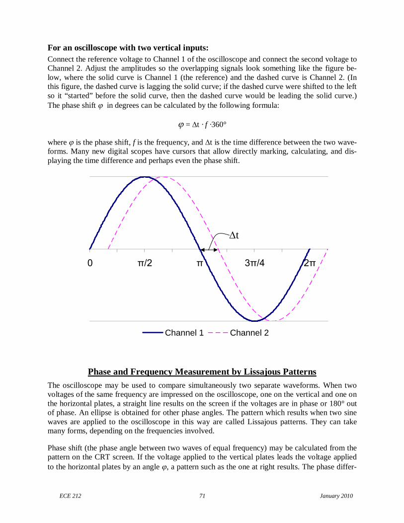
ECE 212 71 January 2010
For an oscilloscope with two vertical inputs:
Connect the reference voltage to Channel 1 of the oscilloscope and connect the second voltage toChannel 2. Adjust the amplitudes so the overlapping signals look something like the figure be-low, where the solid curve is Channel 1 (the reference) and the dashed curve is Channel 2. (Inthis figure, the dashed curve is lagging the solid curve; if the dashed curve were shifted to the leftso it “started” before the solid curve, then the dashed curve would be leading the solid curve.)The phase shift in degrees can be calculated by the following formula:
= t · f ·360°
where is the phase shift, f is the frequency, and t is the time difference between the two wave-forms. Many new digital scopes have cursors that allow directly marking, calculating, and dis-playing the time difference and perhaps even the phase shift.
0 π/2 π 3π/4 2π
Channel 1 Channel 2
Phase and Frequency Measurement by Lissajous Patterns
The oscilloscope may be used to compare simultaneously two separate waveforms. When twovoltages of the same frequency are impressed on the oscilloscope, one on the vertical and one onthe horizontal plates, a straight line results on the screen if the voltages are in phase or 180° outof phase. An ellipse is obtained for other phase angles. The pattern which results when two sinewaves are applied to the oscilloscope in this way are called Lissajous patterns. They can takemany forms, depending on the frequencies involved.
Phase shift (the phase angle between two waves of equal frequency) may be calculated from thepattern on the CRT screen. If the voltage applied to the vertical plates leads the voltage appliedto the horizontal plates by an angle , a pattern such as the one at right results. The phase differ-
t
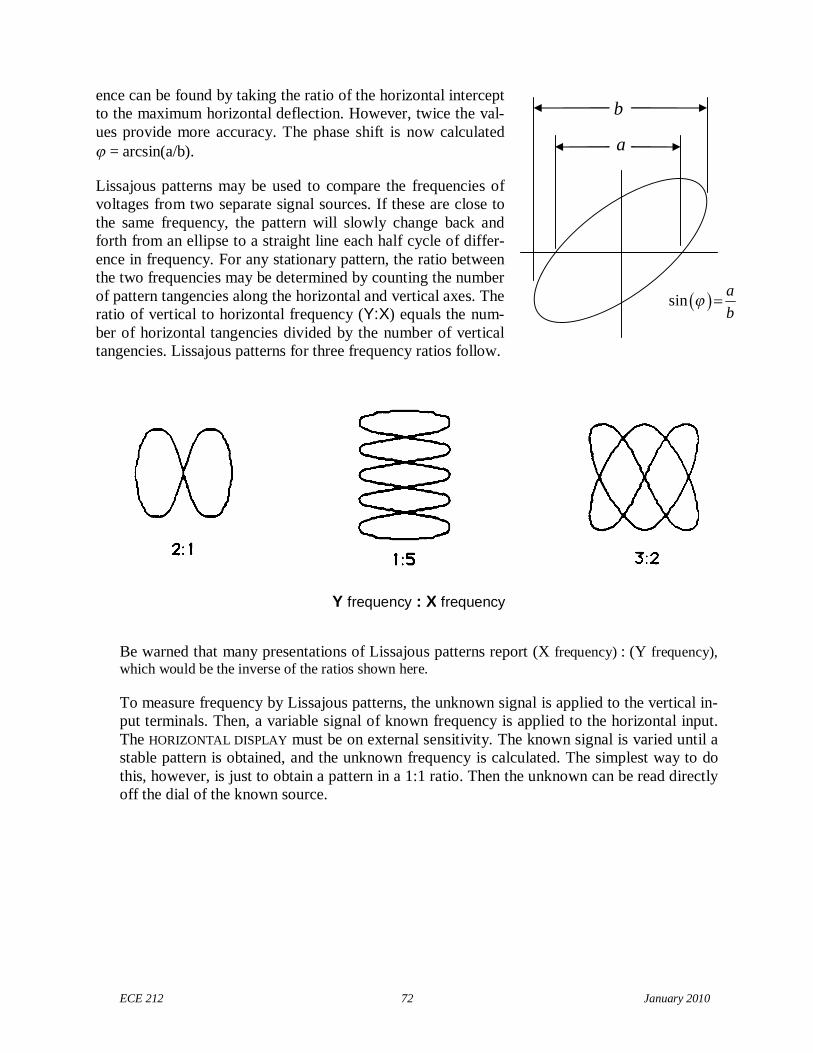
ECE 212 72 January 2010
a
b
sina
b
ence can be found by taking the ratio of the horizontal interceptto the maximum horizontal deflection. However, twice the val-ues provide more accuracy. The phase shift is now calculated = arcsin(a/b).
Lissajous patterns may be used to compare the frequencies ofvoltages from two separate signal sources. If these are close tothe same frequency, the pattern will slowly change back andforth from an ellipse to a straight line each half cycle of differ-ence in frequency. For any stationary pattern, the ratio betweenthe two frequencies may be determined by counting the numberof pattern tangencies along the horizontal and vertical axes. Theratio of vertical to horizontal frequency (Y:X) equals the num-ber of horizontal tangencies divided by the number of verticaltangencies. Lissajous patterns for three frequency ratios follow.
Be warned that many presentations of Lissajous patterns report (X frequency) : (Y frequency),which would be the inverse of the ratios shown here.
To measure frequency by Lissajous patterns, the unknown signal is applied to the vertical in-put terminals. Then, a variable signal of known frequency is applied to the horizontal input.The HORIZONTAL DISPLAY must be on external sensitivity. The known signal is varied until astable pattern is obtained, and the unknown frequency is calculated. The simplest way to dothis, however, is just to obtain a pattern in a 1:1 ratio. Then the unknown can be read directlyoff the dial of the known source.
Y frequency : X frequency
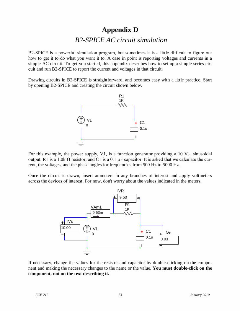
ECE 212 73 January 2010
Appendix D
B2-SPICE AC circuit simulation
B2-SPICE is a powerful simulation program, but sometimes it is a little difficult to figure outhow to get it to do what you want it to. A case in point is reporting voltages and currents in asimple AC circuit. To get you started, this appendix describes how to set up a simple series cir-cuit and run B2-SPICE to report the current and voltages in that circuit.
Drawing circuits in B2-SPICE is straightforward, and becomes easy with a little practice. Startby opening B2-SPICE and creating the circuit shown below.
0
V1
1KR1
0.1u
C1
For this example, the power supply, V1, is a function generator providing a 10 VPP sinusoidaloutput. R1 is a 1.0k Ω resistor, and C1 is a 0.1 µF capacitor. It is asked that we calculate the cur-rent, the voltages, and the phase angles for frequencies from 500 Hz to 5000 Hz.
Once the circuit is drawn, insert ammeters in any branches of interest and apply voltmetersacross the devices of interest. For now, don't worry about the values indicated in the meters.
0
V1
1KR1
0.1u
C1
9.53m
VAm1
9.53
IVR
3.03
IVc
10.00
IVs
If necessary, change the values for the resistor and capacitor by double-clicking on the compo-nent and making the necessary changes to the name or the value. You must double-click on thecomponent, not on the text describing it.
ECE 212 74 January 2010
Set the power supply voltage by double-clicking on the round icon representing the voltagesource. Change the part title to “V1” if necessary. Set the [DC VALUE] to 0.
Select the [SMALL SIGNAL AC AND DISTORTION] tab. Under [AC PROPERTIES FOR AC SMALL SIGNAL
ANALYSIS ONLY], enter magnitude 10 V and phase 0. Check [USE]. Click [OK].
Set the range of frequencies to be simulated as follows: Click in the circuit window to be sure itis selected. Click on the menu item [SIMULATION] and then choose [SET UP SIMULATIONS]. Clickon the button [AC (AC FREQUENCY SWEEP)]. Make the following entries:
Start Value 500 (the frequency at which you want to begin)
Stop Value 5000 (the frequency at which you want to stop)
Number of Each Steps per Interval 10 (the number of frequencies at which you want cal-culations, beginning at the Start Value and ending atthe Stop Value.)
Stepping interval Linear
Check (i.e., select) [SHOW APTITUDE PLOTS] and [SHOW PHASE PLOTS].
Select [USE DEGREES FOR PLOTS] and [USE MAGNITUDE FOR PLOTS].
Check [DISPLAY GRAPH].
Check [DISPLAY TABLE].
Click [OK].
Be sure that [AC (AC FREQUENCY SWEEP)] is enabled.
Then click the button marked [RUN NOW...].
Immediately a table of voltages, currents, and phase angles will be displayed from 500 Hz to5000 Hz. The phase angles may be a bit misleading for our purposes, because they force the sup-ply voltage to have a phase angle of zero (0), while our usual procedure is to require the voltageand current of the resistor to point along the real (X) axis in our phasor diagrams. Nonetheless,the simulation data show the relative phases of the voltages, and as expected, the current throughthe capacitor leads the voltage across the capacitor by 90°.
B2-SPICE will create a graph of the data, if you checked DISPLAY GRAPH, but the voltage andcurrent scales are usually so small that they require magnification. One can overcome the displayproblem in the simulation by multiplying the simulation’s supply voltage by some constant sothat it is near 100V. Be sure to correct for the multiplicative constant if you try to extract magni-tude values from the graph later.
To graph the table of data in Excel, EXPORT the table to a text file (through the File menu), andthen read that text file into Excel. Once the data is in Excel, use the search and replace functionto change units multipliers:k to E3m to E-3u to E-6n to E-9

meg to E6
Excel recognizes the E# as equivalent to 10^#, where # is an appropriate number. Be sure you donot put any blank spaces in the substitution, or Excel will think it is all text.
After the substitutions are completed, use the standard Excel commands to graph the columns ofinterest. In this case you would probably choose an XY scatterplot VC and VR magnitudes versusfrequency.
O
Tq
S
DTab
S
CcIa
Cvwo
Warning: NEVER copy the simulated values and pretend that they are your calculations oryour measurements. That is cheating. Whenever you report values from a simulation, be sure tostate that they are from the simulation and what program you used to do that simulation. To dootherwise is to be dishonest.
ECE 212 75 January 2010
scilloscope-like Display
o have B2-SPICE show an oscilloscope-like display of the circuit’s voltages and currents, re-uires only a few changes.
et up the circuit as before, and add meters for anything you want measured.
ouble-click on the voltage source. In the [TRANSIENT PROPERTIES] section select [SINUSOIDAL].o the right, click on the [PEAK AMPLITUDE OF VOLTAGE] and in the [VALUE] box, enter “10”nd click [ACCEPT NEW VALUE]. Then click on [FREQUENCY] and enter “500” in the [VALUE]ox and click [ACCEPT NEW VALUE]. Click [OK].
etting the simulation parameters
lick on the circuit drawing to be sure it is selected. From the menu click on [Simulation] andhoose [Set up Simulations]. Enable [Transient and Fourier Analyses] and then click that button.nput a reasonable STOP TIME that will show a few cycles. In this case the frequency is 500 Hz,nd so a stop time of 0.01 seconds will display five cycles. Enable [Display Graph]. Click [OK].
lick the button marked [RUN NOW...]. Immediately B2-SPICE will generate a graph of whateveroltages and currents you had meters for on the circuit layout. If [AC (AC FREQUENCY SWEEP)]as also still enabled, then B2-SPICE would also generate that graph and table of data. The bestf both worlds.