Embed Size (px)
Citation preview
ECE 2162Memory
Views of Memory
•Real machines have limited amounts of memory– 640KB? A few GB?– (This laptop = 2GB)
• Programmer doesn’t want to be bothered– Do you think, “oh, this computer only has 128MB
so I’ll write my code this way…”– What happens if you run on a different machine?
2
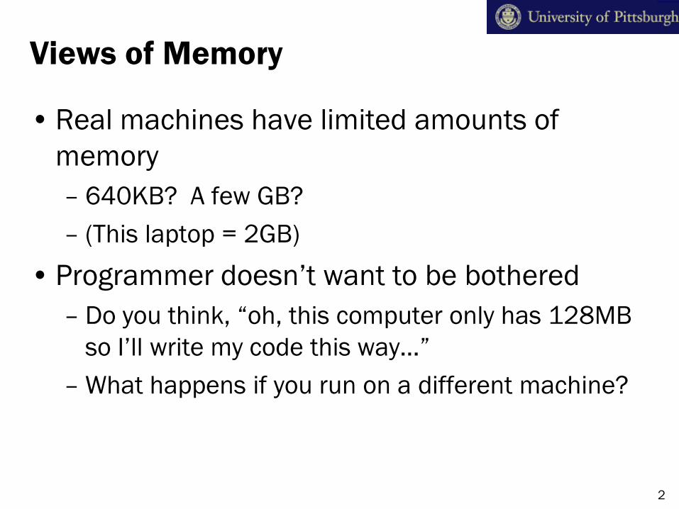
Programmer’s View
• Example 32-bit memory– When programming, you
don’t care about how much real memory there is
– Even if you use a lot, memory can always be paged to disk
Kernel
Text
Data
Heap
Stack
0-2GB
4GBAKA Virtual Addresses
3
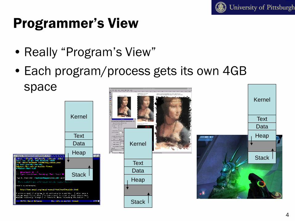
Programmer’s View
•Really “Program’s View”• Each program/process gets its own 4GB
space
Kernel
TextDataHeap
Stack
Kernel
TextDataHeap
Stack
Kernel
TextDataHeap
Stack
4
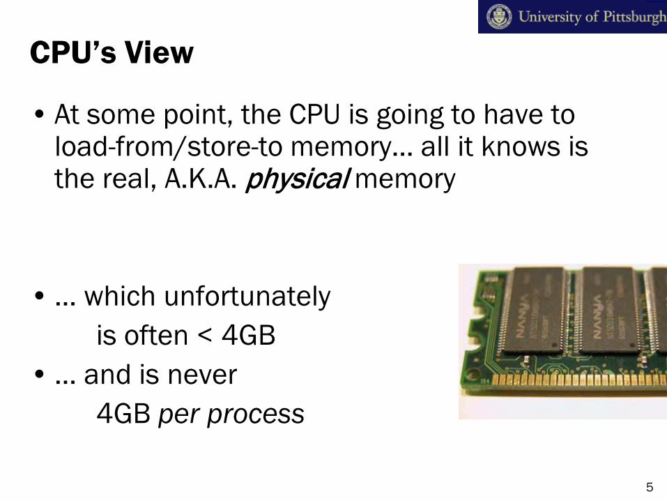
CPU’s View
• At some point, the CPU is going to have to load-from/store-to memory… all it knows is the real, A.K.A. physical memory
•… which unfortunatelyis often < 4GB
•… and is never4GB per process
5
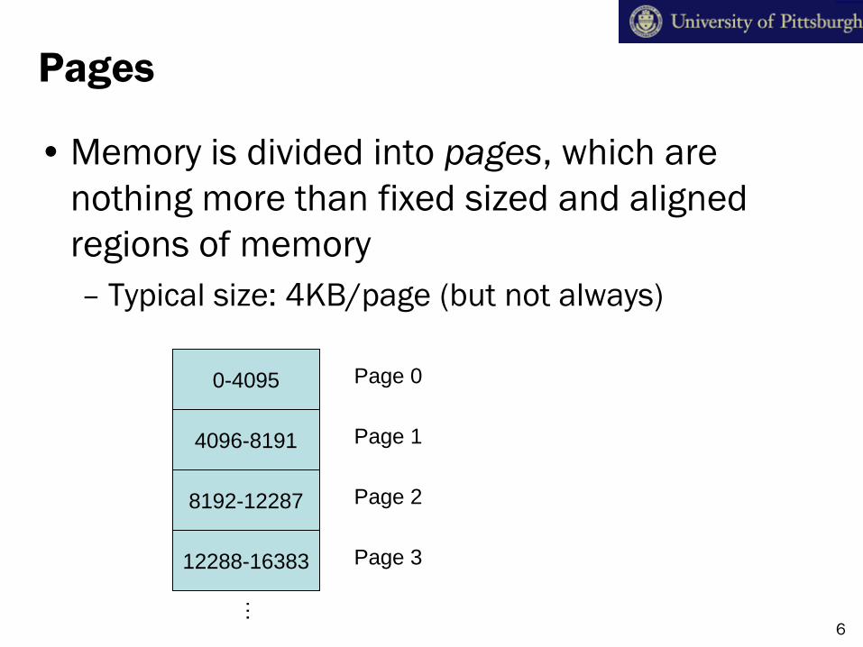
Pages
•Memory is divided into pages, which are nothing more than fixed sized and aligned regions of memory– Typical size: 4KB/page (but not always)
0-4095
4096-8191
8192-12287
12288-16383
…
Page 0
Page 1
Page 2
Page 3
6
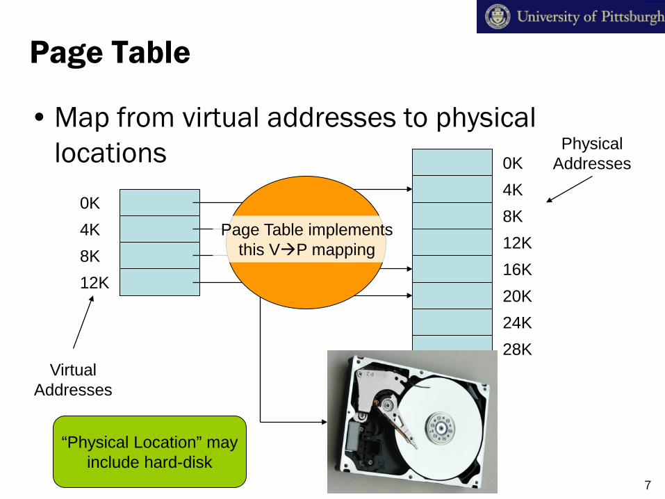
Page Table
•Map from virtual addresses to physical locations
0K4K8K12K
VirtualAddresses
0K4K8K12K16K20K24K28K
PhysicalAddresses
“Physical Location” mayinclude hard-disk
Page Table implementsthis VP mapping
7
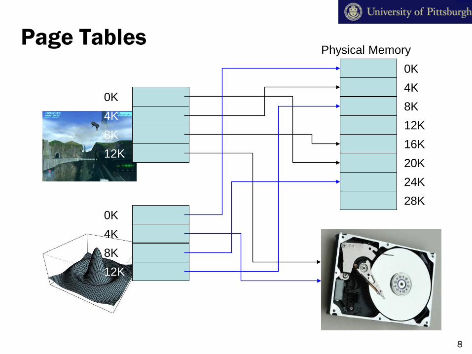
Page Tables
0K4K8K12K
0K4K8K12K16K20K24K28K
0K4K8K12K
Physical Memory
8
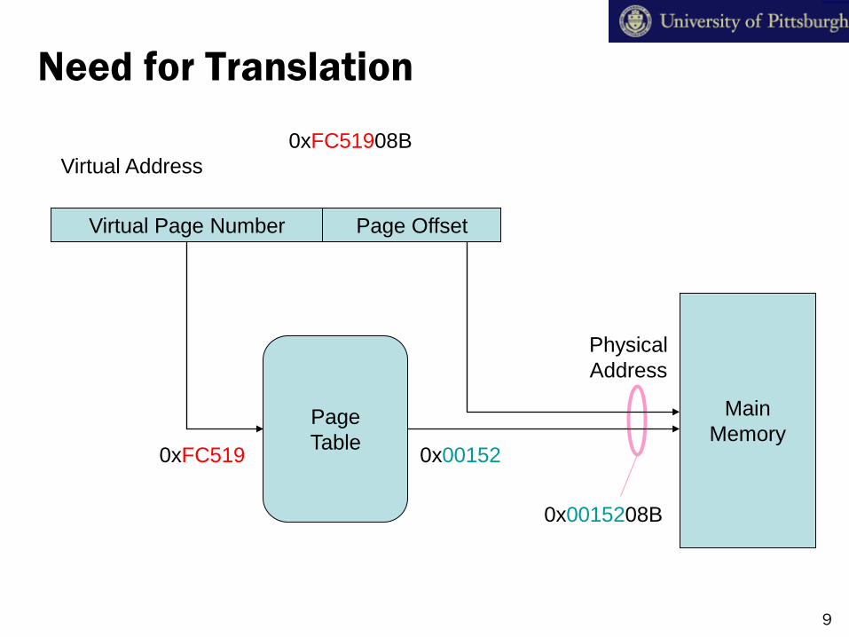
Need for Translation
Virtual Address
Virtual Page Number Page Offset
PageTable
MainMemory
PhysicalAddress
0xFC51908B
0x001520xFC519
0x0015208B
9
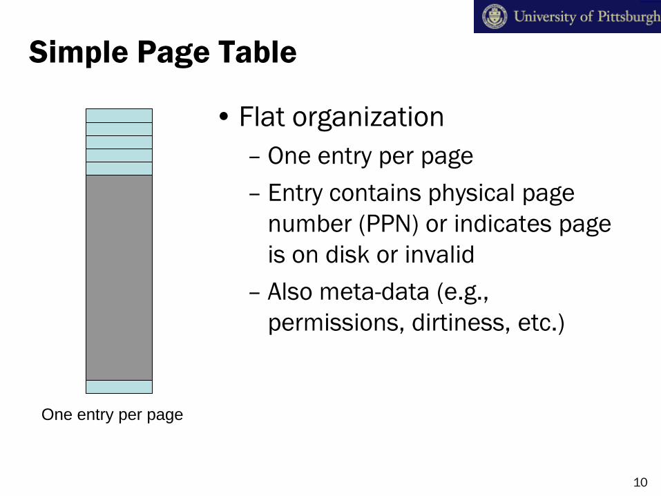
Simple Page Table
• Flat organization– One entry per page– Entry contains physical page
number (PPN) or indicates page is on disk or invalid
– Also meta-data (e.g., permissions, dirtiness, etc.)
One entry per page
10
Multi-Level Page Tables
•Break up the virtual address space into multiple page tables
• Increase the utilization and reduce the physical size of a page table
• A simple technique is a two-level page table
11
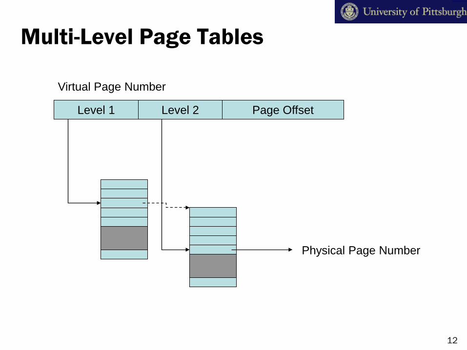
Multi-Level Page Tables
Level 1 Level 2 Page Offset
Physical Page Number
Virtual Page Number
12
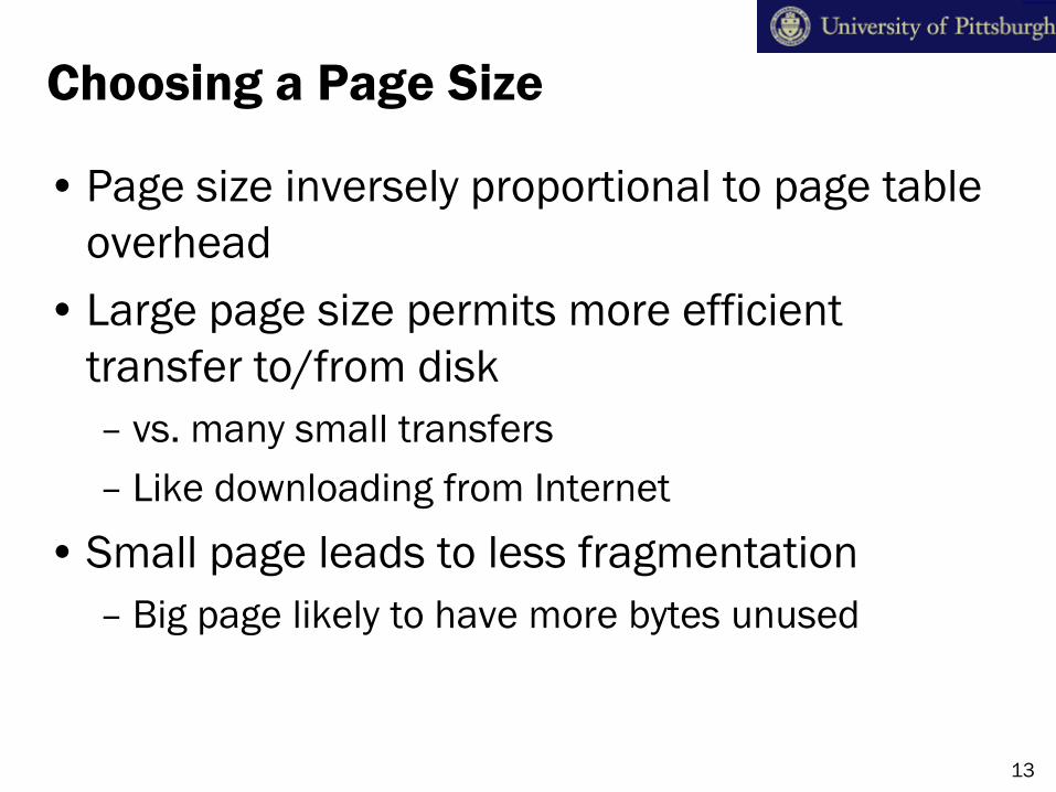
Choosing a Page Size
• Page size inversely proportional to page table overhead
• Large page size permits more efficient transfer to/from disk– vs. many small transfers– Like downloading from Internet
• Small page leads to less fragmentation– Big page likely to have more bytes unused
13
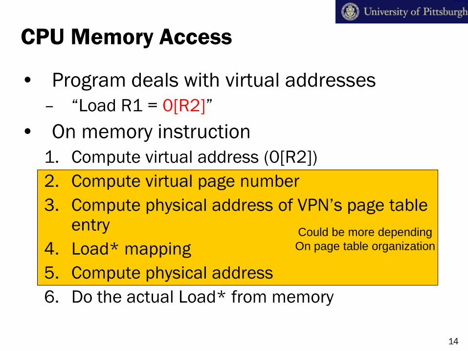
CPU Memory Access
• Program deals with virtual addresses– “Load R1 = 0[R2]”
• On memory instruction1. Compute virtual address (0[R2])2. Compute virtual page number3. Compute physical address of VPN’s page table
entry4. Load* mapping 5. Compute physical address6. Do the actual Load* from memory
Could be more dependingOn page table organization
14
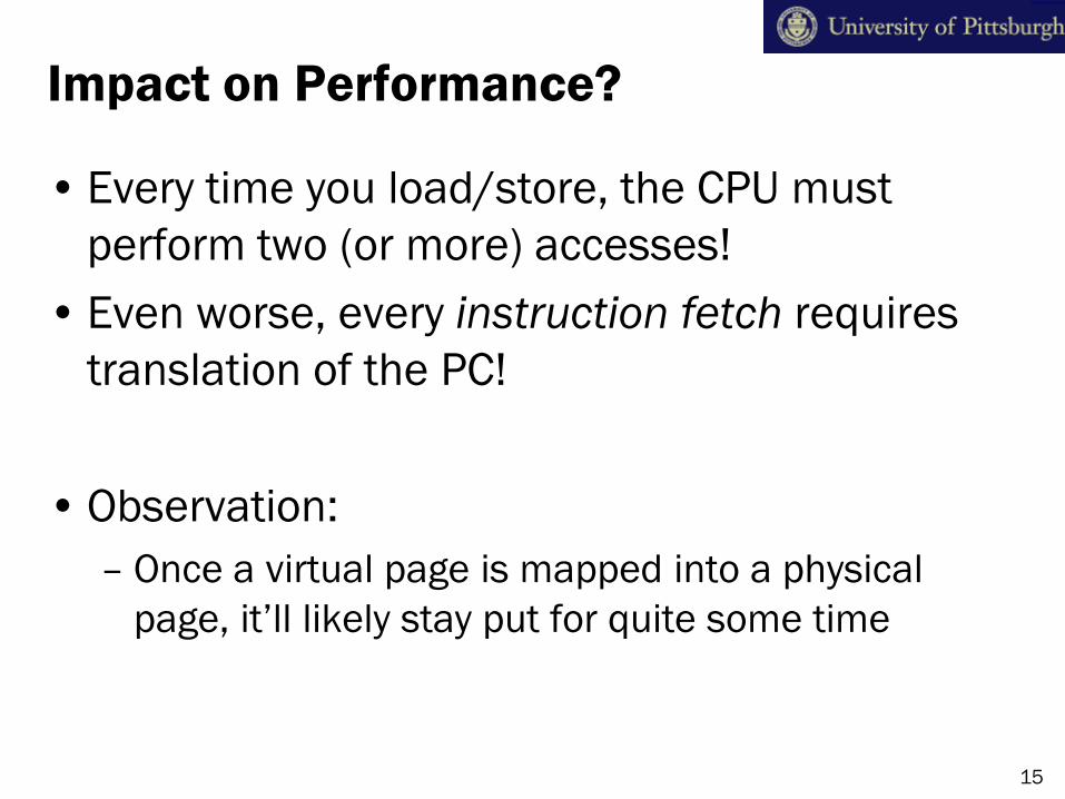
Impact on Performance?
• Every time you load/store, the CPU must perform two (or more) accesses!
• Even worse, every instruction fetch requires translation of the PC!
•Observation:– Once a virtual page is mapped into a physical
page, it’ll likely stay put for quite some time
15
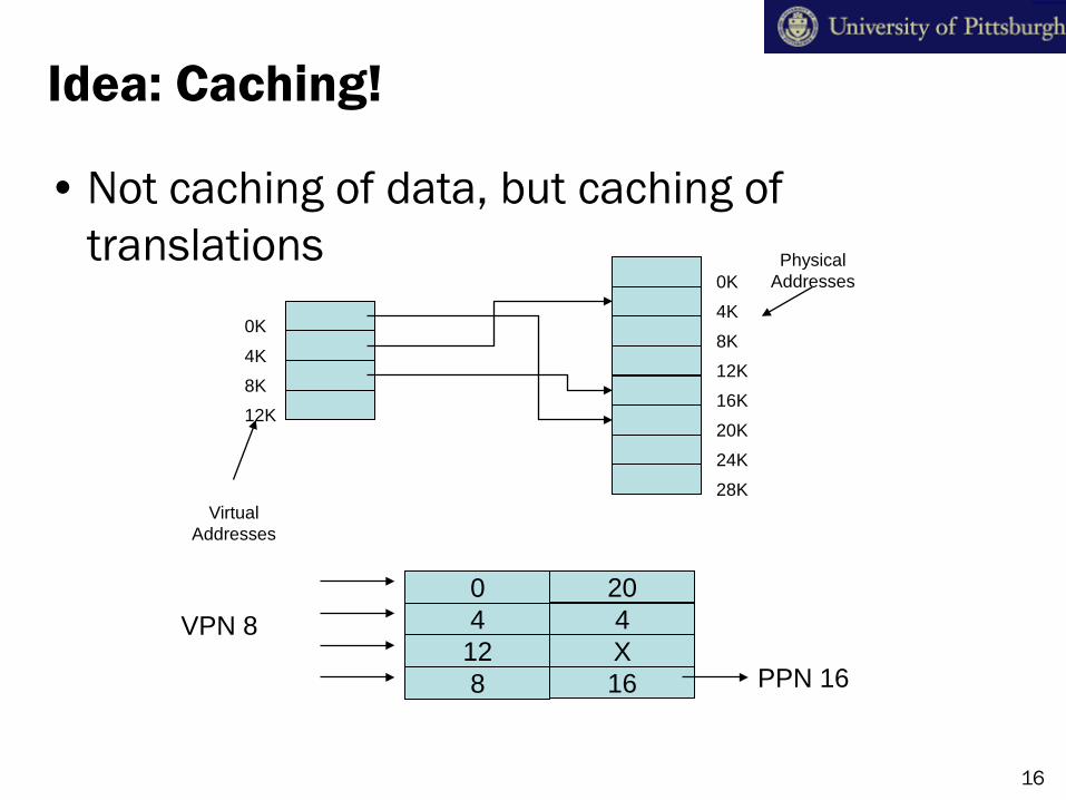
Idea: Caching!
•Not caching of data, but caching of translations
0K
4K
8K12K
VirtualAddresses
0K
4K
8K
12K
16K
20K
24K
28K
PhysicalAddresses
8 16
0 204 4
12 XVPN 8
PPN 16
16
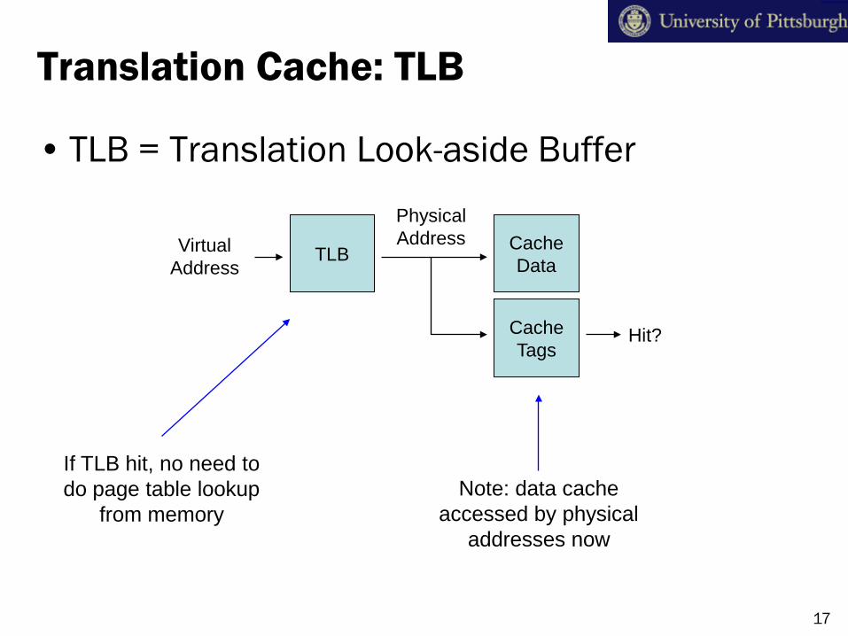
Translation Cache: TLB
• TLB = Translation Look-aside Buffer
TLBVirtualAddress
CacheData
PhysicalAddress
CacheTags
Hit?
If TLB hit, no need todo page table lookup
from memoryNote: data cache
accessed by physicaladdresses now
17
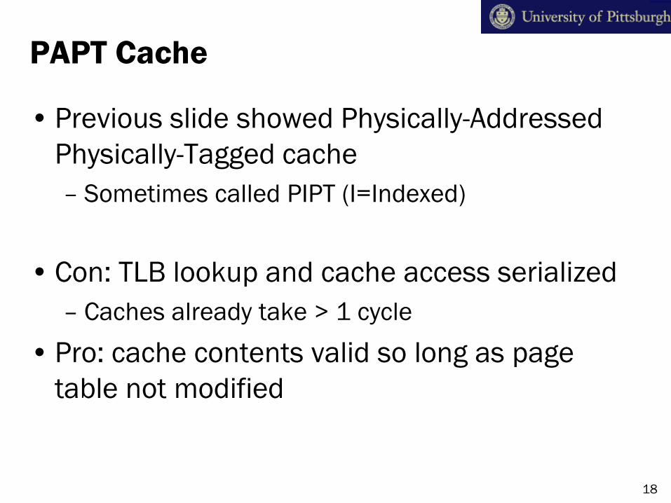
PAPT Cache
• Previous slide showed Physically-Addressed Physically-Tagged cache– Sometimes called PIPT (I=Indexed)
• Con: TLB lookup and cache access serialized– Caches already take > 1 cycle
• Pro: cache contents valid so long as page table not modified
18
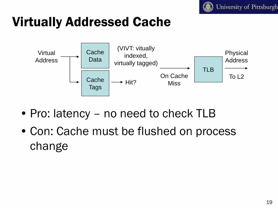
Virtually Addressed Cache
VirtualAddress
CacheData
CacheTags
Hit?
• Pro: latency – no need to check TLB• Con: Cache must be flushed on process
change
(VIVT: vituallyindexed,
virtually tagged)TLB
On CacheMiss
PhysicalAddress
To L2
19
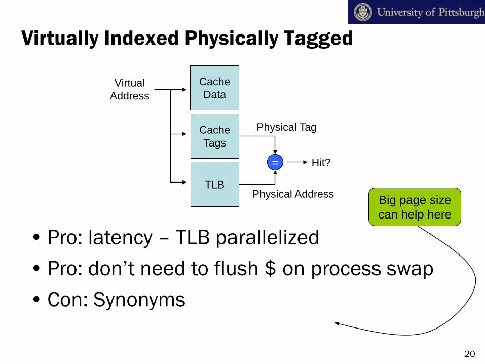
Virtually Indexed Physically Tagged
VirtualAddress
CacheData
CacheTags
Hit?
• Pro: latency – TLB parallelized• Pro: don’t need to flush $ on process swap• Con: Synonyms
TLBPhysical Address
=
Physical Tag
Big page sizecan help here
20
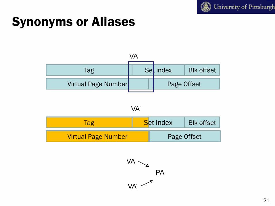
Synonyms or Aliases
Tag Set index Blk offset
VA
Virtual Page Number Page Offset
Virtual Page Number Page Offset
Tag Blk offsetSet Index
VA’
VA
VA’
PA
21
TLB Design
•Often fully-associative– For latency, this means few entries– However, each entry is for a whole page– Ex. 32-entry TLB, 4KB page… how big of working
set while avoiding TLB misses?
• If many misses:– Increase TLB size (latency problems)– Increase page size (fragmenation problems)
22
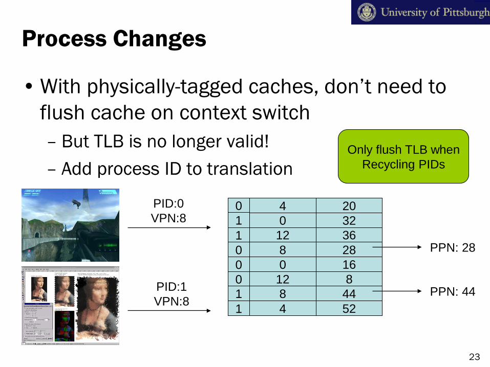
Process Changes
•With physically-tagged caches, don’t need to flush cache on context switch– But TLB is no longer valid!– Add process ID to translation
8 28
4 200 32
12 36
0110
4 52
0 1612 88 44
0011
PID:0VPN:8
PPN: 28
PID:1VPN:8
PPN: 44
Only flush TLB whenRecycling PIDs
23
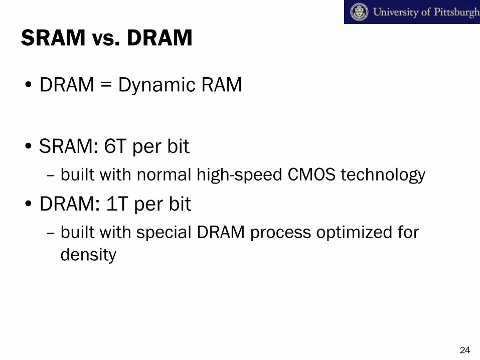
SRAM vs. DRAM
•DRAM = Dynamic RAM
• SRAM: 6T per bit– built with normal high-speed CMOS technology
•DRAM: 1T per bit– built with special DRAM process optimized for
density
24
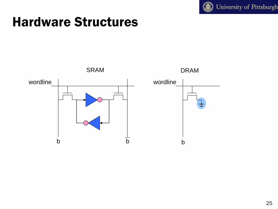
Hardware Structures
b b
SRAM
wordline
b
DRAM
wordline
25
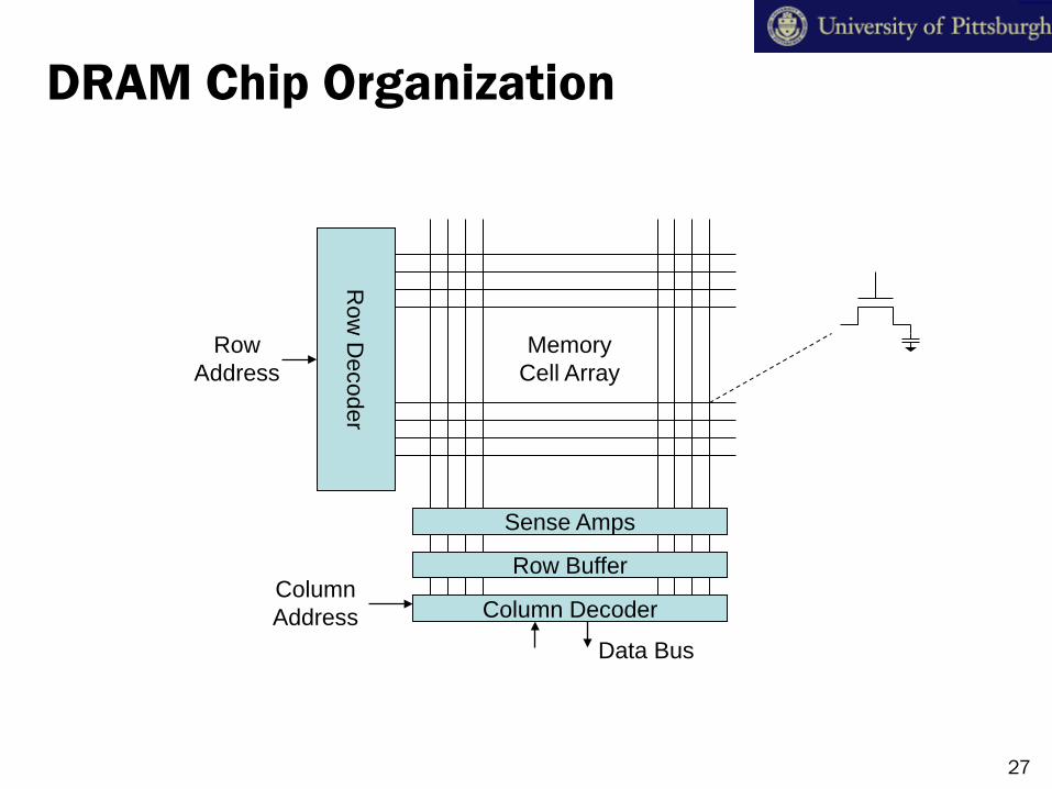
DRAM Chip Organization
Row
Decoder
Sense Amps
Column Decoder
MemoryCell Array
Row Buffer
RowAddress
ColumnAddress
Data Bus
27
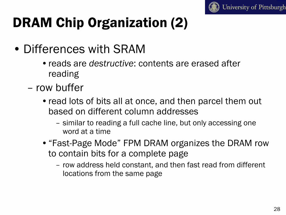
DRAM Chip Organization (2)
•Differences with SRAM•reads are destructive: contents are erased after
reading– row buffer
•read lots of bits all at once, and then parcel them out based on different column addresses
– similar to reading a full cache line, but only accessing one word at a time
•“Fast-Page Mode” FPM DRAM organizes the DRAM row to contain bits for a complete page
– row address held constant, and then fast read from different locations from the same page
28
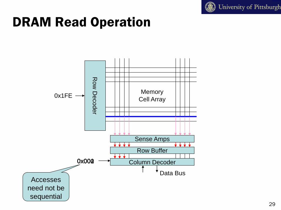
DRAM Read Operation
Row
Decoder
Sense Amps
Column Decoder
MemoryCell Array
Row Buffer
0x1FE
0x000
Data Bus
0x0010x002
Accesses need not be sequential
29
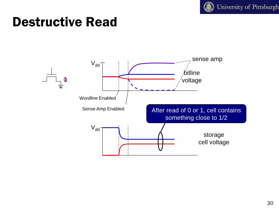
Destructive Read
1
Vdd
Wordline Enabled
Sense Amp Enabled
bitlinevoltage
Vddstorage
cell voltage
sense amp
0
After read of 0 or 1, cell containssomething close to 1/2
30
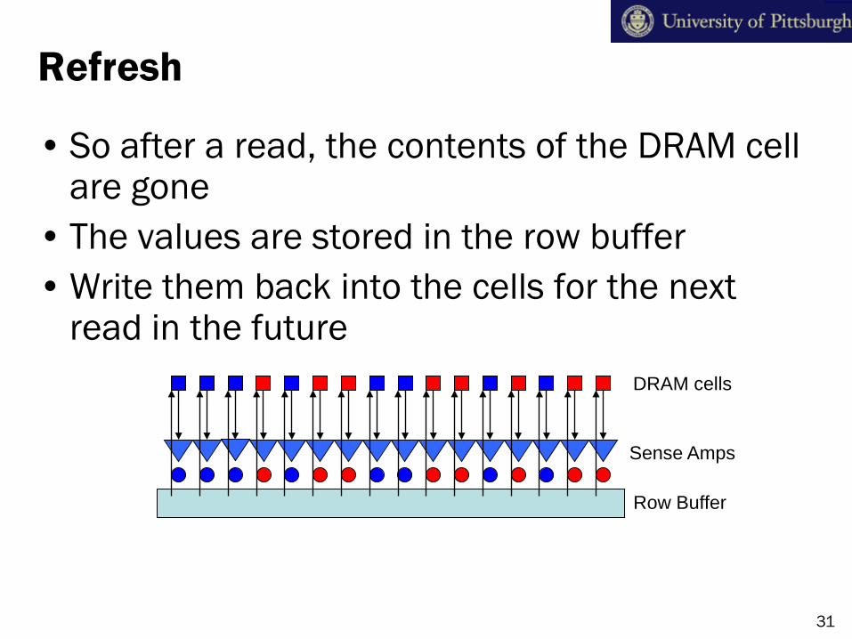
Refresh
• So after a read, the contents of the DRAM cell are gone
• The values are stored in the row buffer•Write them back into the cells for the next
read in the future
Row Buffer
Sense Amps
DRAM cells
31
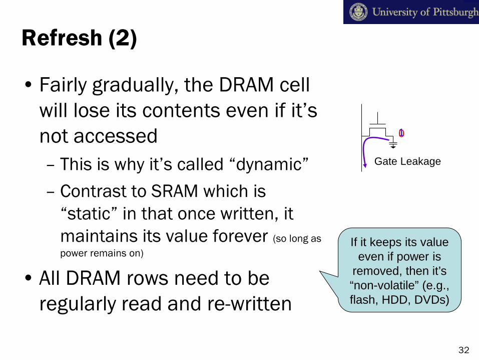
Refresh (2)
• Fairly gradually, the DRAM cell will lose its contents even if it’s not accessed– This is why it’s called “dynamic”– Contrast to SRAM which is
“static” in that once written, it maintains its value forever (so long as power remains on)
• All DRAM rows need to be regularly read and re-written
1
Gate Leakage
0
If it keeps its value even if power is
removed, then it’s “non-volatile” (e.g., flash, HDD, DVDs)
32
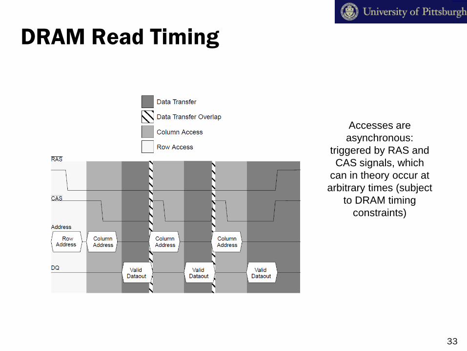
DRAM Read Timing
Accesses areasynchronous:
triggered by RAS andCAS signals, which
can in theory occur atarbitrary times (subject
to DRAM timingconstraints)
33
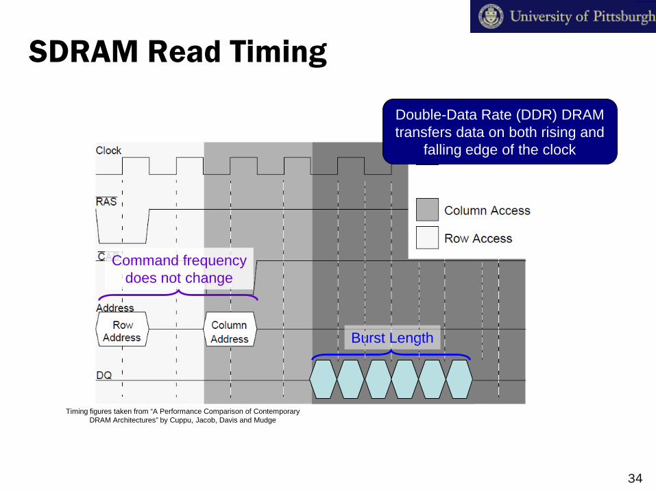
SDRAM Read Timing
Burst Length
Double-Data Rate (DDR) DRAMtransfers data on both rising and
falling edge of the clock
Timing figures taken from “A Performance Comparison of ContemporaryDRAM Architectures” by Cuppu, Jacob, Davis and Mudge
Command frequencydoes not change
34
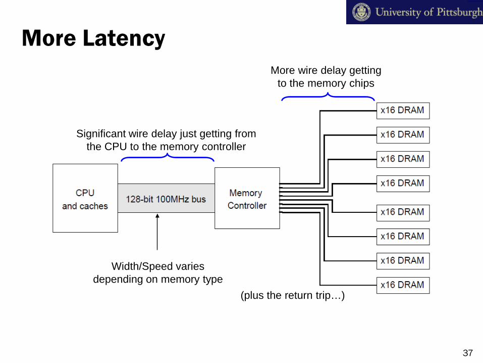
More Latency
Width/Speed variesdepending on memory type
Significant wire delay just getting fromthe CPU to the memory controller
More wire delay gettingto the memory chips
(plus the return trip…)
37
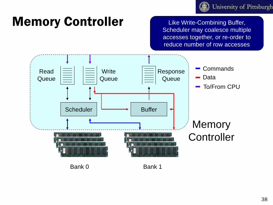
Memory Controller
MemoryController
Scheduler Buffer
Bank 0 Bank 1
CommandsData
ReadQueue
WriteQueue
ResponseQueue
To/From CPU
Like Write-Combining Buffer,Scheduler may coalesce multipleaccesses together, or re-order toreduce number of row accesses
38
Memory Reference Scheduling
• Just like registers, need to enforce RAW, WAW, WAR dependencies
•No “memory renaming” in memory controller, so enforce all three dependencies
• Like everything else, still need to maintain appearance of sequential access– Consider multiple read/write requests to the
same address
39
Faster DRAM Speed
• Clock FSB faster– DRAM chips may not be able to keep up
•Latency dominated by wire delay
– Bandwidth may be improved (DDR vs. regular) but latency doesn’t change much• Instead of 2 cycles for row access, may take 3 cycles at
a faster bus speed
•Doesn’t address latency of the memory access
42
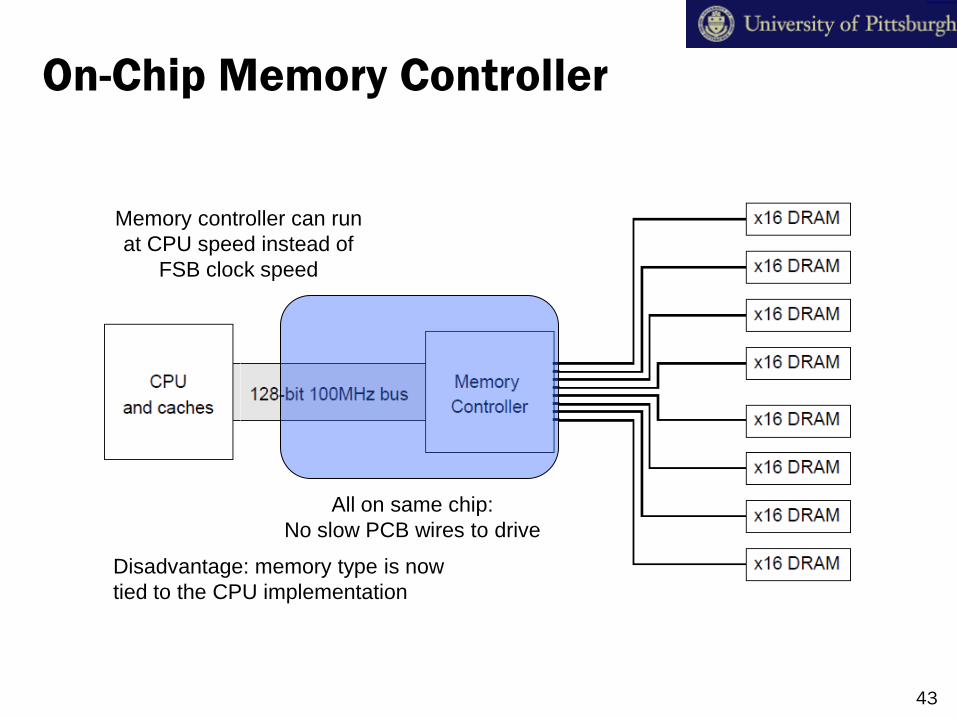
On-Chip Memory Controller
All on same chip:No slow PCB wires to drive
Memory controller can runat CPU speed instead of
FSB clock speed
Disadvantage: memory type is nowtied to the CPU implementation
43
Read 5.3 in the text
44