Embed Size (px)
Citation preview
EECS 247- Lecture 16 DAC Design (continued)- Introduction to ADCs © 2008 H.K. Page 1
EE247Lecture 16
• DAC Converters (continued)– DAC design considerations– Self calibration techniques
• Current copiers• Dynamic element matching
– DAC reconstruction filter• ADC Converters
– Sampling• Sampling switch considerations
– Thermal noise due to switch resistance– Sampling switch bandwidth limitations– Switch induced distortion
• Sampling switch conductance dependence on input voltage• Clock voltage boosters
EECS 247- Lecture 16 DAC Design (continued)- Introduction to ADCs © 2008 H.K. Page 2
2μ tech., 5Vsupply6+2 segmented8x8 array
EECS 247- Lecture 16 DAC Design (continued)- Introduction to ADCs © 2008 H.K. Page 3
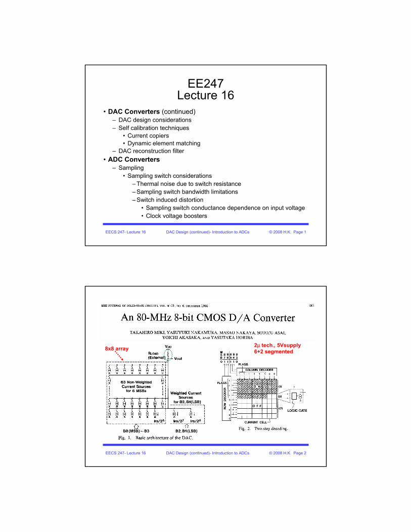
Current-Switched DACs in CMOS
Iout
Example: 5 unit element current sources
VDD
I1 I2 I3 I4
Rx4I Rx3I Rx2I
M1 M2 M3 M4 I5M5
RxI
Assumptions:RxI small compared to transistor gate-overdriveTo simplify analysis: Initially, all device currents assumed to be equal to I
( )
M 2 M 1
M 3 M 1
M 4 M 1
M 5 M 1
M 2
M 1
GS GS
GS GS
GS GS
GS GS
2GS th2
2
2 1GS th
V V 4RI
V V 7RI
V V 9RI
V V 10RI
V VI k
4RI1I IV V
⎛ ⎞⎜ ⎟⎜ ⎟⎝ ⎠
= −
= −
= −
= −
−=
−=−
VG
EECS 247- Lecture 16 DAC Design (continued)- Introduction to ADCs © 2008 H.K. Page 4
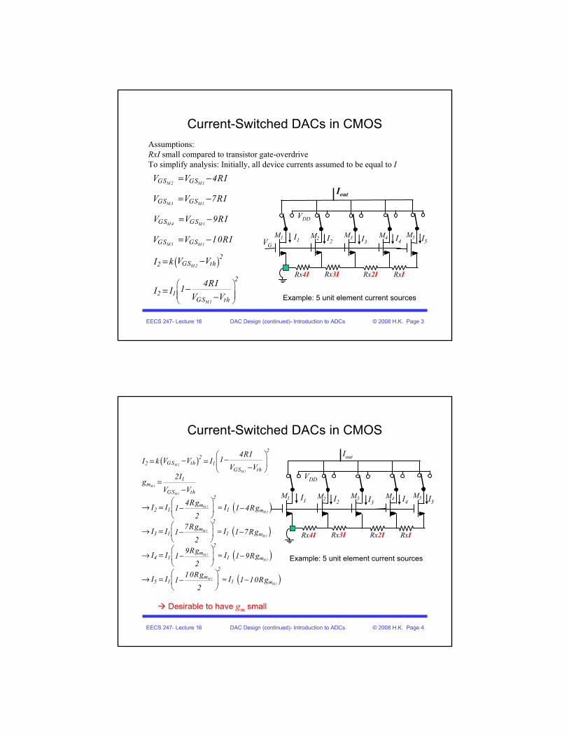
Current-Switched DACs in CMOS
Iout
Desirable to have gm small
Example: 5 unit element current sources
VDD
I1 I2 I3 I4
Rx4I Rx3I Rx2I
M1 M2 M3 M4 I5M5
RxI
( )
( )
( )
( )
( )
M 2
M 1
M 1
M 1
M 1M 1
M 1M 1
M 1M 1
M 1M 1
22
GS th2 1GS th
1m
GS th2
m2 1 1 m
2m
3 1 1 m
2m
4 1 1 m
2m
5 1 1 m
4RI1V VI k I
V V2I
gV V
4RgI I I 1 4Rg12
7RgI I I 1 7Rg12
9RgI I I 1 9Rg12
10RgI I I 1 10Rg12
⎛ ⎞−−= = ⎜ ⎟−⎝ ⎠=
−⎛ ⎞
→ = ≈ −−⎜ ⎟⎝ ⎠⎛ ⎞
→ = ≈ −−⎜ ⎟⎝ ⎠⎛ ⎞
→ = ≈ −−⎜ ⎟⎝ ⎠⎛ ⎞
→ = ≈ −−⎜ ⎟⎝ ⎠
EECS 247- Lecture 16 DAC Design (continued)- Introduction to ADCs © 2008 H.K. Page 5
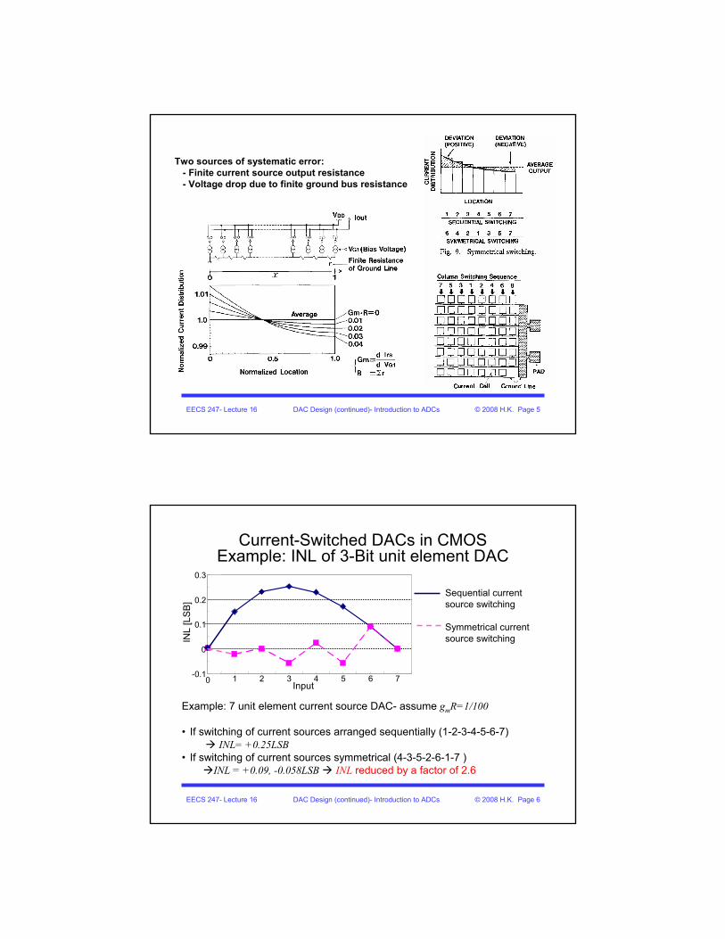
Two sources of systematic error:- Finite current source output resistance- Voltage drop due to finite ground bus resistance
EECS 247- Lecture 16 DAC Design (continued)- Introduction to ADCs © 2008 H.K. Page 6
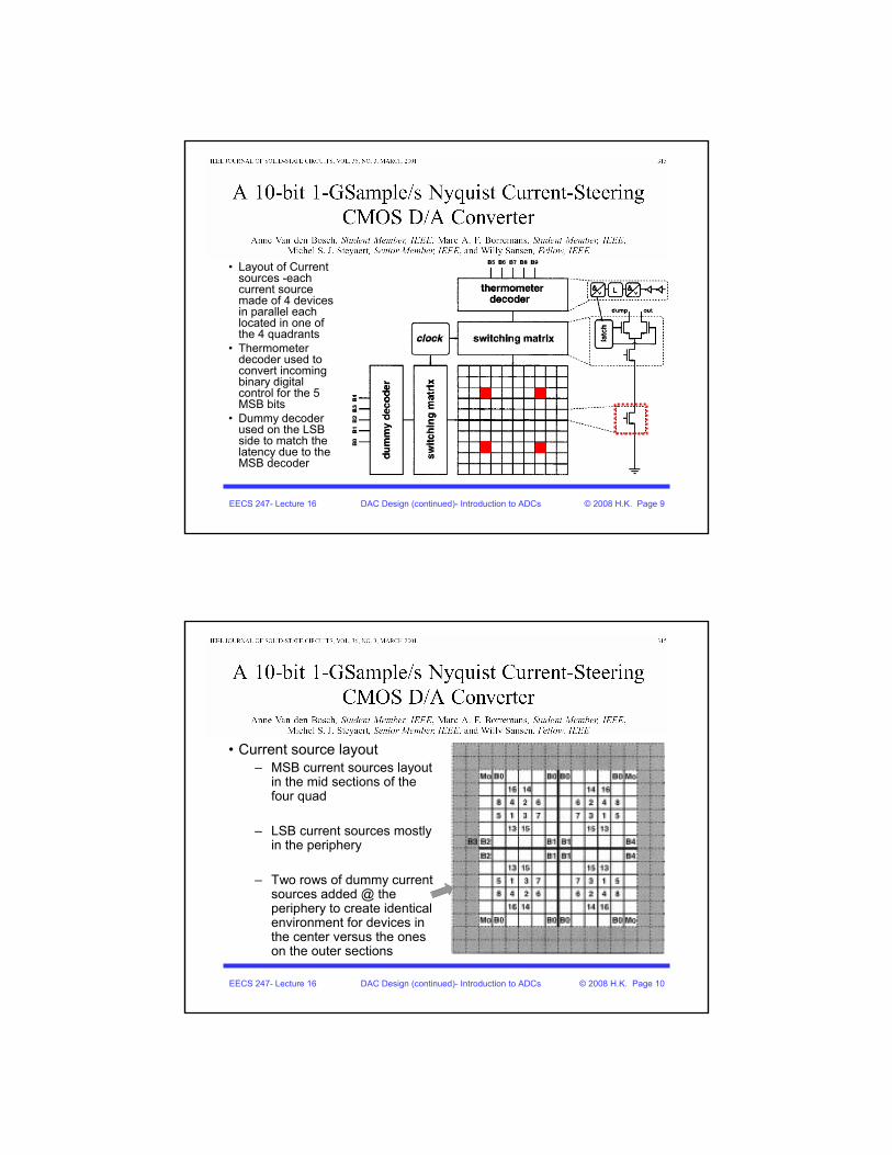
Current-Switched DACs in CMOSExample: INL of 3-Bit unit element DAC
Input
INL
[LS
B]
Example: 7 unit element current source DAC- assume gmR=1/100
• If switching of current sources arranged sequentially (1-2-3-4-5-6-7)INL= +0.25LSB
• If switching of current sources symmetrical (4-3-5-2-6-1-7 )INL = +0.09, -0.058LSB INL reduced by a factor of 2.6
-0.1
0
0.1
0.2
0.3
1 2 3 4 5 6 70
Sequential current source switching
Symmetrical current source switching

EECS 247- Lecture 16 DAC Design (continued)- Introduction to ADCs © 2008 H.K. Page 7
Current-Switched DACs in CMOSExample: DNL of 7 unit element DAC
Input
DN
L [L
SB
]
Example: 7 unit element current source DAC- assume gmR=1/100
• If switching of current sources arranged sequentially (1-2-3-4-5-6-7)DNLmax= + 0.15LSB
• If switching of current sources symmetrical (4-3-5-2-6-1-7 )
DNLmax = + 0.15LSB DNLmax unchanged
-0.2
-0.1
0
0.1
0.2
1 2 3 4 5 6 7
Sequential current source switching
Symmetrical current source switching
EECS 247- Lecture 16 DAC Design (continued)- Introduction to ADCs © 2008 H.K. Page 8
More recent published DAC using symmetrical switching built in 0.35μ/3V analog/1.9V digital, area x10 smaller compared to previous example
(5+5)
EECS 247- Lecture 16 DAC Design (continued)- Introduction to ADCs © 2008 H.K. Page 9
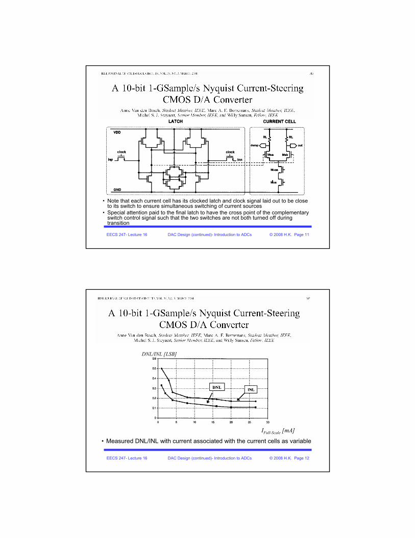
• Layout of Current sources -each current source made of 4 devices in parallel each located in one of the 4 quadrants
• Thermometer decoder used to convert incoming binary digital control for the 5 MSB bits
• Dummy decoder used on the LSB side to match the latency due to the MSB decoder
EECS 247- Lecture 16 DAC Design (continued)- Introduction to ADCs © 2008 H.K. Page 10
• Current source layout– MSB current sources layout
in the mid sections of the four quad
– LSB current sources mostly in the periphery
– Two rows of dummy current sources added @ the periphery to create identical environment for devices in the center versus the ones on the outer sections
EECS 247- Lecture 16 DAC Design (continued)- Introduction to ADCs © 2008 H.K. Page 11
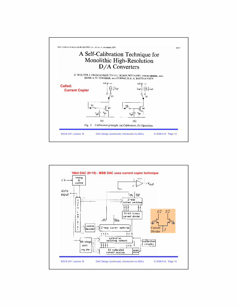
• Note that each current cell has its clocked latch and clock signal laid out to be close to its switch to ensure simultaneous switching of current sources
• Special attention paid to the final latch to have the cross point of the complementary switch control signal such that the two switches are not both turned off during transition
EECS 247- Lecture 16 DAC Design (continued)- Introduction to ADCs © 2008 H.K. Page 12
• Measured DNL/INL with current associated with the current cells as variable
DNL/INL [LSB]
IFull-Scale [mA]
EECS 247- Lecture 16 DAC Design (continued)- Introduction to ADCs © 2008 H.K. Page 13
Called: Current Copier
EECS 247- Lecture 16 DAC Design (continued)- Introduction to ADCs © 2008 H.K. Page 14
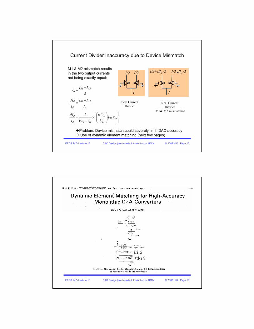
I
I/2 I/2
Current Divider
16bit DAC (6+10) - MSB DAC uses current copier technique
EECS 247- Lecture 16 DAC Design (continued)- Introduction to ADCs © 2008 H.K. Page 15
I
I/2 I/2
Ideal Current Divider
Current Divider Inaccuracy due to Device Mismatch
I
I/2+dId /2
Real Current Divider
M1& M2 mismatched
I/2-dId /2
M1 M2M1 M2
Problem: Device mismatch could severely limit DAC accuracyUse of dynamic element matching (next few pages)
M1 & M2 mismatch results in the two output currents not being exactly equal:
d1 d2d
d d1 d2
d d
WLd
thWLd GS th
I II
2
dI I I
I I
ddI 2dV
I V V
+=
−=
⎡ ⎤⎛ ⎞= × +⎢ ⎥⎜ ⎟
− ⎝ ⎠⎣ ⎦
EECS 247- Lecture 16 DAC Design (continued)- Introduction to ADCs © 2008 H.K. Page 16
EECS 247- Lecture 16 DAC Design (continued)- Introduction to ADCs © 2008 H.K. Page 17
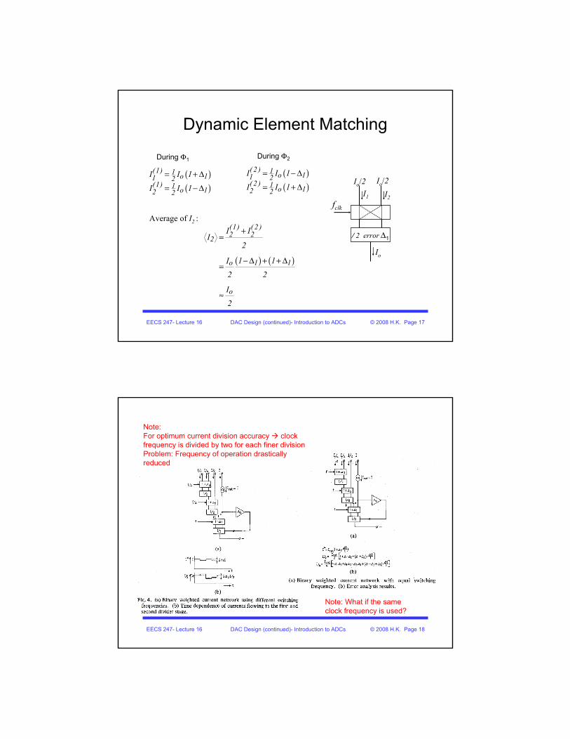
Dynamic Element Matching
( ) ( )
(1) ( 2 )2 22
1 1o
o
I II
2
1 1I2 2
I2
+=
− Δ + + Δ=
≈
( )( )
(1) 1 o 11 2(1) 1 o 12 2
I I 1
I I 1
= + Δ
= − Δ
/ 2 error Δ1
I1
During Φ1 During Φ2
I2fclk
Io
Io/2Io/2( )( )
( 2 ) 1 o 11 2( 2 ) 1 o 12 2
I I 1
I I 1
= − Δ
= + Δ
Average of I2 :
EECS 247- Lecture 16 DAC Design (continued)- Introduction to ADCs © 2008 H.K. Page 18
Note: For optimum current division accuracy clock frequency is divided by two for each finer divisionProblem: Frequency of operation drastically reduced
Note: What if the same clock frequency is used?
EECS 247- Lecture 16 DAC Design (continued)- Introduction to ADCs © 2008 H.K. Page 19
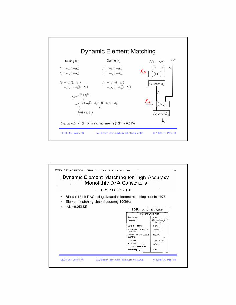
Dynamic Element Matching
( )( )
( )( )( )214
1
2)1(
121)1(
3
121)1(
2
121)1(
1
111
1
1
Δ+Δ+=Δ+=
Δ−=
Δ+=
o
o
o
III
II
II ( )( )
( )( )( )214
1
2)2(
121)2(
3
121)2(
2
121)2(
1
111
1
1
Δ−Δ−=Δ−=
Δ+=
Δ−=
o
o
o
III
II
II
During Φ1 During Φ2
( )( ) ( )( )
( )21
2121
)2(3
)1(3
3
14
21111
4
2
ΔΔ+=
Δ−Δ−+Δ+Δ+=
+=
o
o
I
I
III
E.g. Δ1 = Δ2 = 1% matching error is (1%)2 = 0.01%
/ 2 error Δ1
I1
I2
fclk
Io
Io/2
/ 2 error Δ2
I3 I4
fclk
Io/4Io/4
EECS 247- Lecture 16 DAC Design (continued)- Introduction to ADCs © 2008 H.K. Page 20
• Bipolar 12-bit DAC using dynamic element matching built in 1976• Element matching clock frequency 100kHz• INL <0.25LSB!
EECS 247- Lecture 16 DAC Design (continued)- Introduction to ADCs © 2008 H.K. Page 21
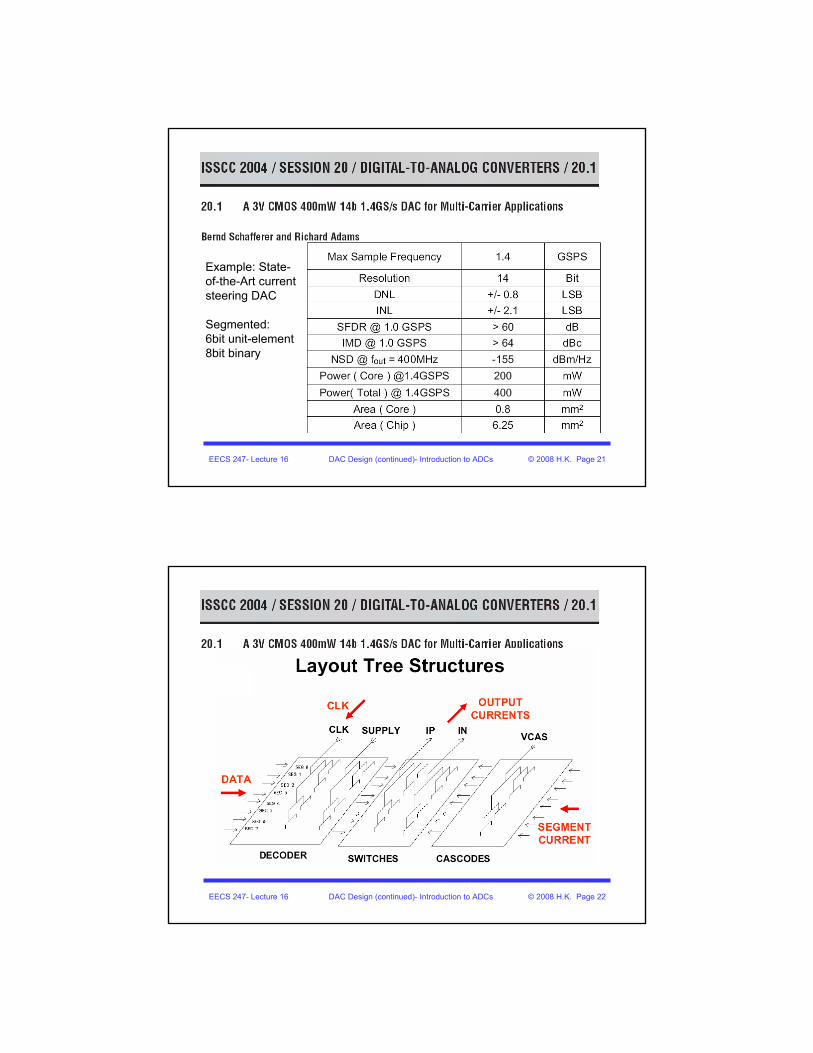
Example: State-of-the-Art current steering DAC
Segmented:6bit unit-element 8bit binary
EECS 247- Lecture 16 DAC Design (continued)- Introduction to ADCs © 2008 H.K. Page 22
EECS 247- Lecture 16 DAC Design (continued)- Introduction to ADCs © 2008 H.K. Page 23
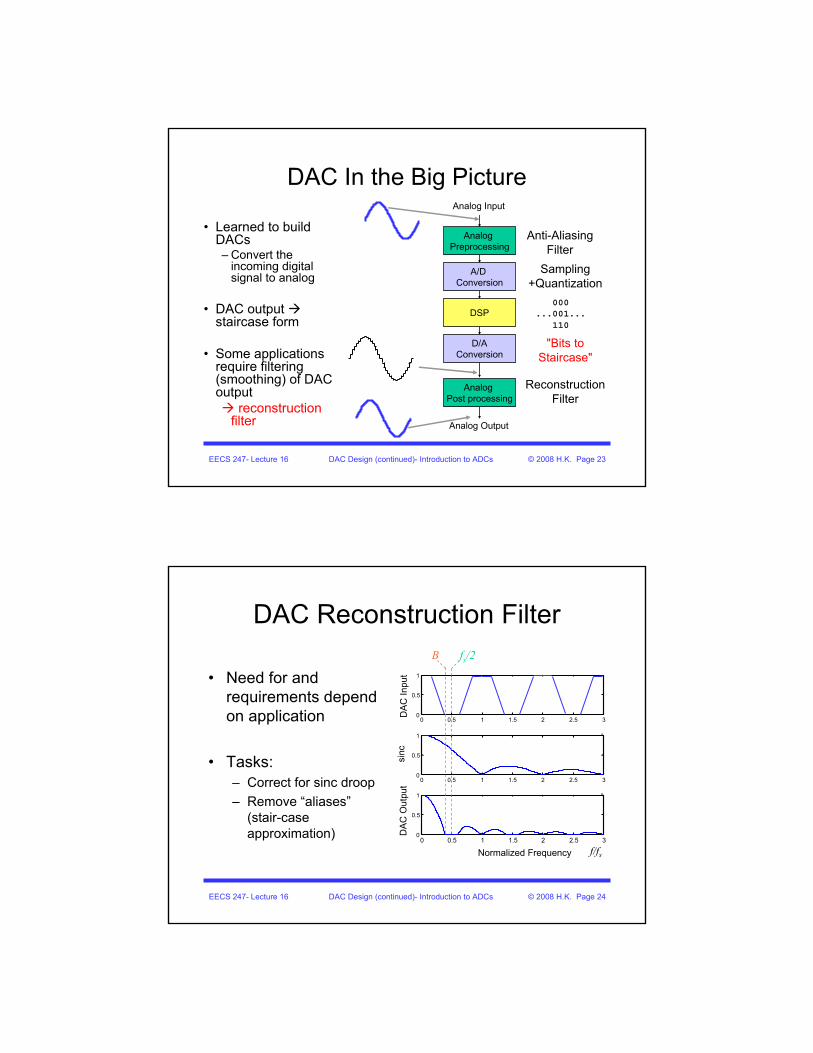
DAC In the Big Picture
• Learned to build DACs– Convert the
incoming digital signal to analog
• DAC output staircase form
• Some applications require filtering (smoothing) of DAC output
reconstruction filter
Analog Post processing
D/AConversion
DSP
A/D Conversion
Analog Preprocessing
Analog Input
Analog Output
000...001...
110
Anti-AliasingFilter
Sampling+Quantization
"Bits to Staircase"
Reconstruction Filter
EECS 247- Lecture 16 DAC Design (continued)- Introduction to ADCs © 2008 H.K. Page 24
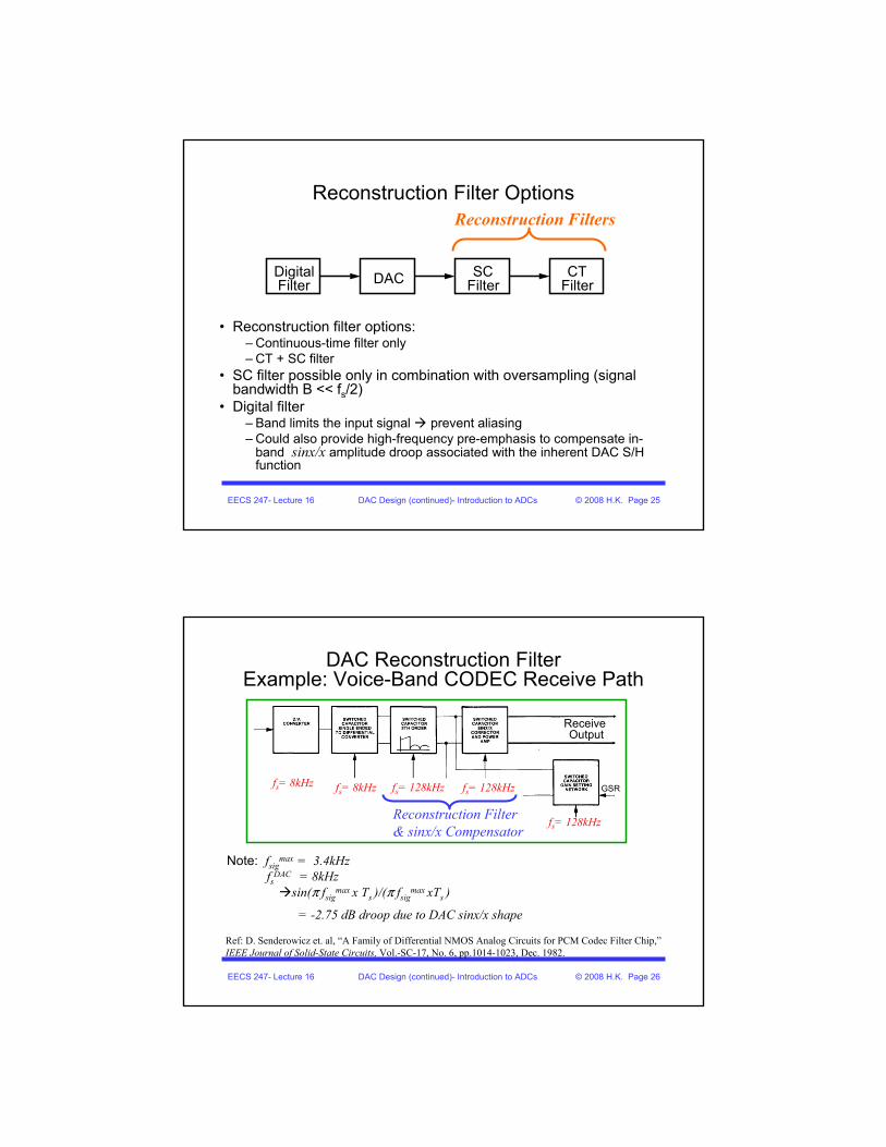
DAC Reconstruction Filter
• Need for and requirements depend on application
• Tasks:– Correct for sinc droop– Remove “aliases”
(stair-case approximation)
B fs/2
0 0.5 1 1.5 2 2.5 3
x 106
0
0.5
1
DAC
Inpu
t
0 0.5 1 1.5 2 2.5 3
x 106
0
0.5
1
sinc
0 0.5 1 1.5 2 2.5 30
0.5
1
DAC
Out
put
Normalized Frequency f/fs
EECS 247- Lecture 16 DAC Design (continued)- Introduction to ADCs © 2008 H.K. Page 25
Reconstruction Filter Options
• Reconstruction filter options:– Continuous-time filter only– CT + SC filter
• SC filter possible only in combination with oversampling (signalbandwidth B << fs/2)
• Digital filter– Band limits the input signal prevent aliasing– Could also provide high-frequency pre-emphasis to compensate in-
band sinx/x amplitude droop associated with the inherent DAC S/H function
DigitalFilter DAC SC
FilterCT
Filter
Reconstruction Filters
EECS 247- Lecture 16 DAC Design (continued)- Introduction to ADCs © 2008 H.K. Page 26
DAC Reconstruction Filter Example: Voice-Band CODEC Receive Path
Ref: D. Senderowicz et. al, “A Family of Differential NMOS Analog Circuits for PCM Codec Filter Chip,”IEEE Journal of Solid-State Circuits, Vol.-SC-17, No. 6, pp.1014-1023, Dec. 1982.
Note: fsigmax = 3.4kHz
fsDAC = 8kHz
sin(π fsigmax x Ts )/(π fsig
max xTs )
= -2.75 dB droop due to DAC sinx/x shape
Receive Output
fs= 8kHz fs= 128kHzfs= 8kHz fs= 128kHz
fs= 128kHz
GSR
Reconstruction Filter& sinx/x Compensator
EECS 247- Lecture 16 DAC Design (continued)- Introduction to ADCs © 2008 H.K. Page 27
SummaryD/A Converter
• D/A architecture – Unit element – complexity proportional to 2B- excellent DNL – Binary weighted- complexity proportional to B- poor DNL– Segmented- unit element MSB(B1)+ binary weighted LSB(B2)
Complexity proportional ((2B1-1) + B2) -DNL compromise between the two• Static performance
– Component matching• Dynamic performance
– Time constants, Glitches• DAC improvement techniques
– Symmetrical switching rather than sequential switching– Current source self calibration– Dynamic element matching
• Depending on the application, reconstruction filter may be needed
EECS 247- Lecture 16 DAC Design (continued)- Introduction to ADCs © 2008 H.K. Page 28
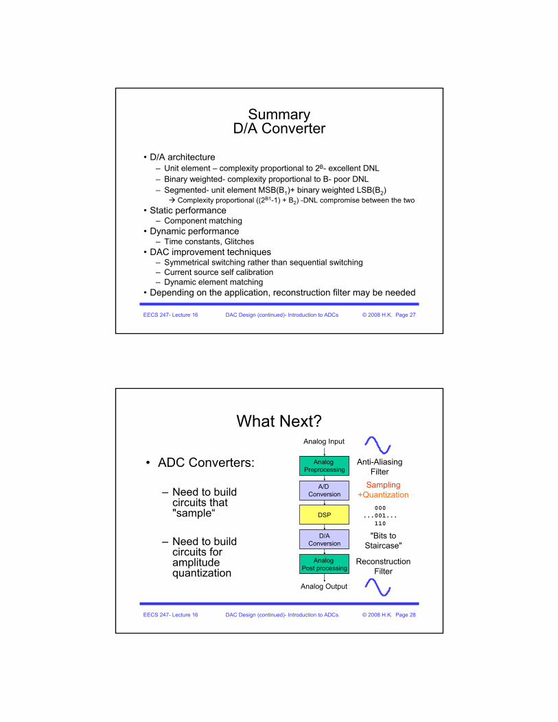
What Next?
• ADC Converters:
– Need to build circuits that "sample“
– Need to build circuits for amplitude quantization
Analog Post processing
D/AConversion
DSP
A/D Conversion
Analog Preprocessing
Analog Input
Analog Output
000...001...
110
Anti-AliasingFilter
Sampling+Quantization
"Bits to Staircase"
Reconstruction Filter
EECS 247- Lecture 16 DAC Design (continued)- Introduction to ADCs © 2008 H.K. Page 29
Analog-to-Digital Converters
• Two categories:– Nyquist rate ADCs fsig
max ~ 0.5xfsampling• Maximum achievable signal bandwidth higher compared
to oversampled type• Resolution limited to max. 12-14bits
– Oversampled ADCs fsigmax << 0.5xfsampling
• Maximum achievable signal bandwidth significantly lower compared to nyquist
• Maximum achievable resolution high (18 to 20bits!)
EECS 247- Lecture 16 DAC Design (continued)- Introduction to ADCs © 2008 H.K. Page 30
MOS Sampling Circuits
EECS 247- Lecture 16 DAC Design (continued)- Introduction to ADCs © 2008 H.K. Page 31
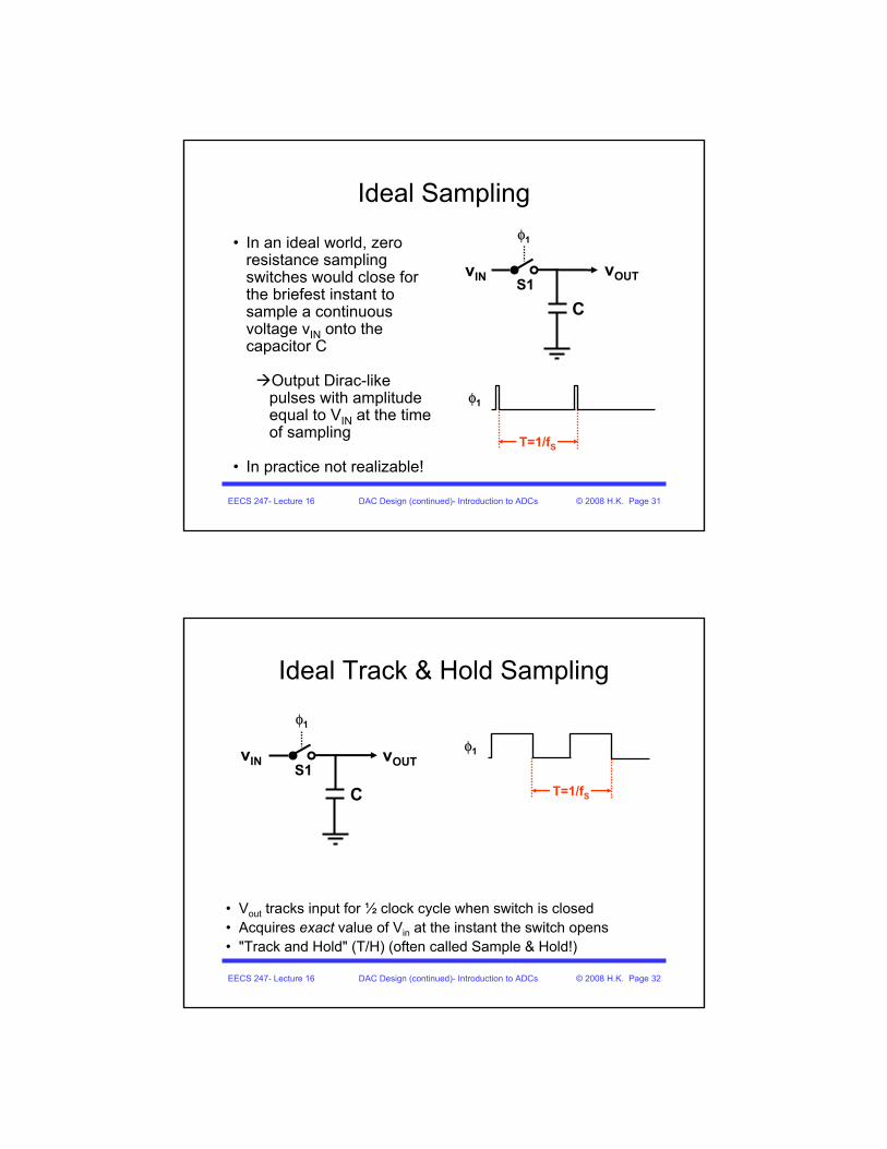
Ideal Sampling
• In an ideal world, zero resistance sampling switches would close for the briefest instant to sample a continuous voltage vIN onto the capacitor C
Output Dirac-like pulses with amplitude equal to VIN at the time of sampling
• In practice not realizable!
vIN vOUT
CS1
φ1
φ1
T=1/fS
EECS 247- Lecture 16 DAC Design (continued)- Introduction to ADCs © 2008 H.K. Page 32
Ideal Track & Hold Sampling
vIN vOUT
CS1
φ1
• Vout tracks input for ½ clock cycle when switch is closed• Acquires exact value of Vin at the instant the switch opens• "Track and Hold" (T/H) (often called Sample & Hold!)
φ1
T=1/fS
EECS 247- Lecture 16 DAC Design (continued)- Introduction to ADCs © 2008 H.K. Page 33
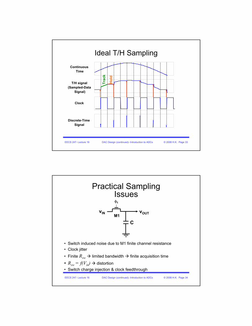
Ideal T/H Sampling
ContinuousTime
T/H signal(Sampled-Data
Signal)
Clock
Discrete-TimeSignal
time
Trac
k
Hol
d
EECS 247- Lecture 16 DAC Design (continued)- Introduction to ADCs © 2008 H.K. Page 34
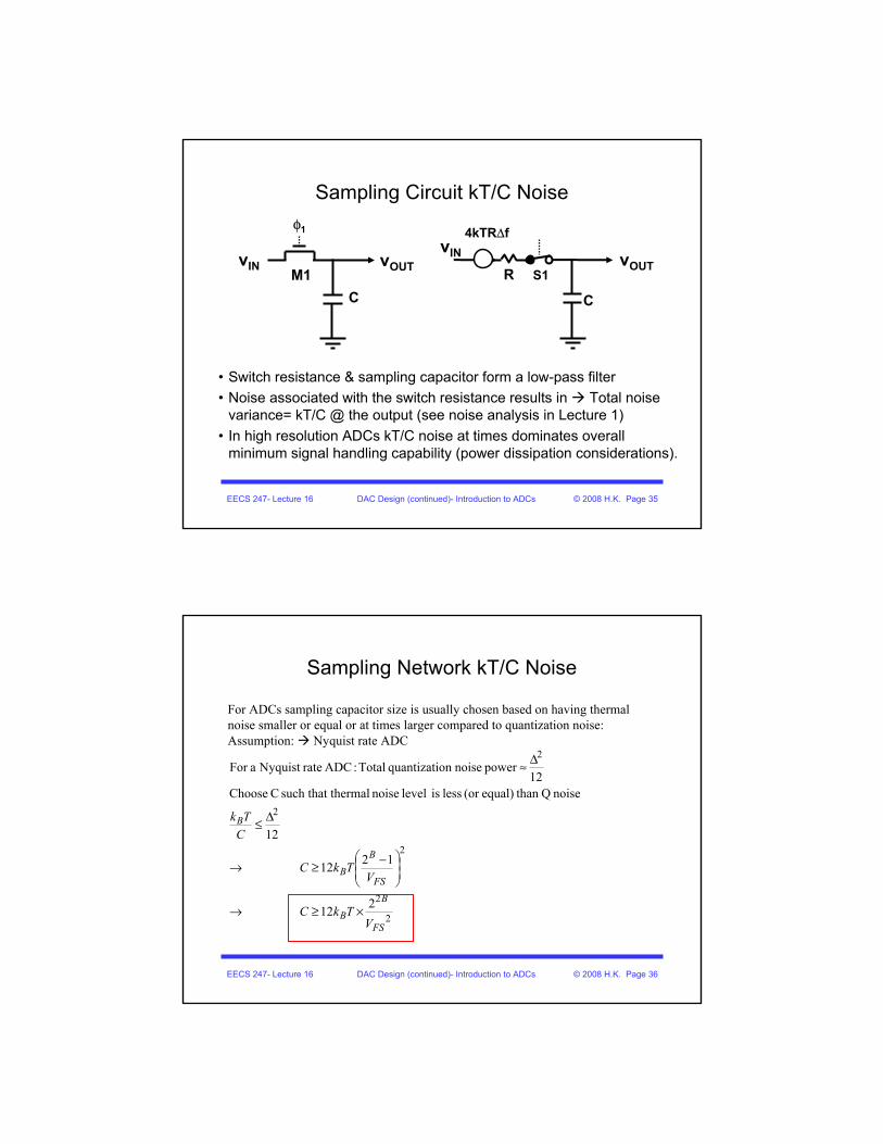
Practical SamplingIssues
vIN vOUT
CM1
φ1
• Switch induced noise due to M1 finite channel resistance• Clock jitter
• Finite Rsw limited bandwidth finite acquisition time
• Rsw = f(Vin) distortion• Switch charge injection & clock feedthrough
EECS 247- Lecture 16 DAC Design (continued)- Introduction to ADCs © 2008 H.K. Page 35
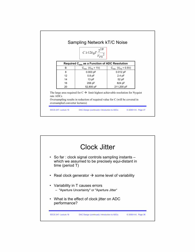
Sampling Circuit kT/C Noise
• Switch resistance & sampling capacitor form a low-pass filter • Noise associated with the switch resistance results in Total noise
variance= kT/C @ the output (see noise analysis in Lecture 1)• In high resolution ADCs kT/C noise at times dominates overall
minimum signal handling capability (power dissipation considerations).
vIN vOUT
C
S1RvIN vOUT
CM1
φ1 4kTRΔf
EECS 247- Lecture 16 DAC Design (continued)- Introduction to ADCs © 2008 H.K. Page 36
Sampling Network kT/C Noise
For ADCs sampling capacitor size is usually chosen based on having thermal noise smaller or equal or at times larger compared to quantization noise:Assumption: Nyquist rate ADC
2
2
2
2
2
212
1212
12
noise Q than equal)(or less is level noise thermalsuch that C Choose12
power noiseon quantizati Total :ADC rateNyquist aFor
FS
B
B
FS
B
B
B
VTkC
VTkC
CTk
×≥→
⎟⎟⎠
⎞⎜⎜⎝
⎛ −≥→
Δ≤
Δ≈
EECS 247- Lecture 16 DAC Design (continued)- Introduction to ADCs © 2008 H.K. Page 37
Sampling Network kT/C Noise
0.012 pF2.4 pF52 pF
824 pF211,200 pF
Cmin (VFS = 0.5V)
Required Cmin as a Function of ADC Resolution
0.003 pF0.8 pF13 pF
206 pF52,800 pF
812141620
Cmin (VFS = 1V)B
2
2212FS
BB
VTkC ≥
The large area required for C limit highest achievable resolution for Nyquist rate ADCs Oversampling results in reduction of required value for C (will be covered in oversampled converter lectures)
EECS 247- Lecture 16 DAC Design (continued)- Introduction to ADCs © 2008 H.K. Page 38
Clock Jitter• So far : clock signal controls sampling instants –
which we assumed to be precisely equi-distant in time (period T)
• Real clock generator some level of variability
• Variability in T causes errors– "Aperture Uncertainty" or "Aperture Jitter“
• What is the effect of clock jitter on ADC performance?

EECS 247- Lecture 16 DAC Design (continued)- Introduction to ADCs © 2008 H.K. Page 39
Clock Jitter
• Sampling jitter adds an error voltage proportional to the product of (tJ-t0) and the derivative of the input signal at the sampling instant
• Does jitter matter when sampling dc signals (x’ (t0 )=0)?
nominal (ideal) sampling
time t0
actualsampling
time tJ
x(t)
x’(t0)
EECS 247- Lecture 16 DAC Design (continued)- Introduction to ADCs © 2008 H.K. Page 40
Clock Jitter
• The error voltage is
nominalsampling
time t0
actualsampling
time tJ
x(t)
x’(t0)
e = x’(t0)(tJ – t0)
error
EECS 247- Lecture 16 DAC Design (continued)- Introduction to ADCs © 2008 H.K. Page 41
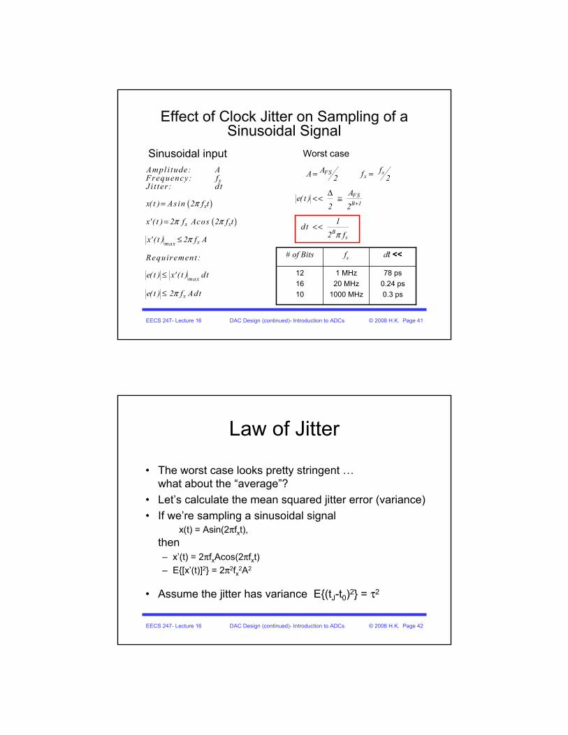
Effect of Clock Jitter on Sampling of a Sinusoidal Signal
Sinusoidal input Worst case
78 ps0.24 ps0.3 ps
1 MHz20 MHz
1000 MHz
121610
dt <<fs# of Bits
sFSx
FSB 1
Bs
fAA f2 2
Ae( t )
2 2
1dt
2 fπ
+
= =
Δ<< ≅
<<
( )
( )
x
x
x x
xmax
max
x
Ampli tude: AFrequency: f J i t ter: d t
x( t ) Asin 2 f t
x' ( t ) 2 f Acos 2 f t
x' ( t ) 2 f A
Requirement:
e( t ) x' ( t ) dt
e( t ) 2 f Adt
π
π π
π
π
=
=
≤
≤
≤
EECS 247- Lecture 16 DAC Design (continued)- Introduction to ADCs © 2008 H.K. Page 42
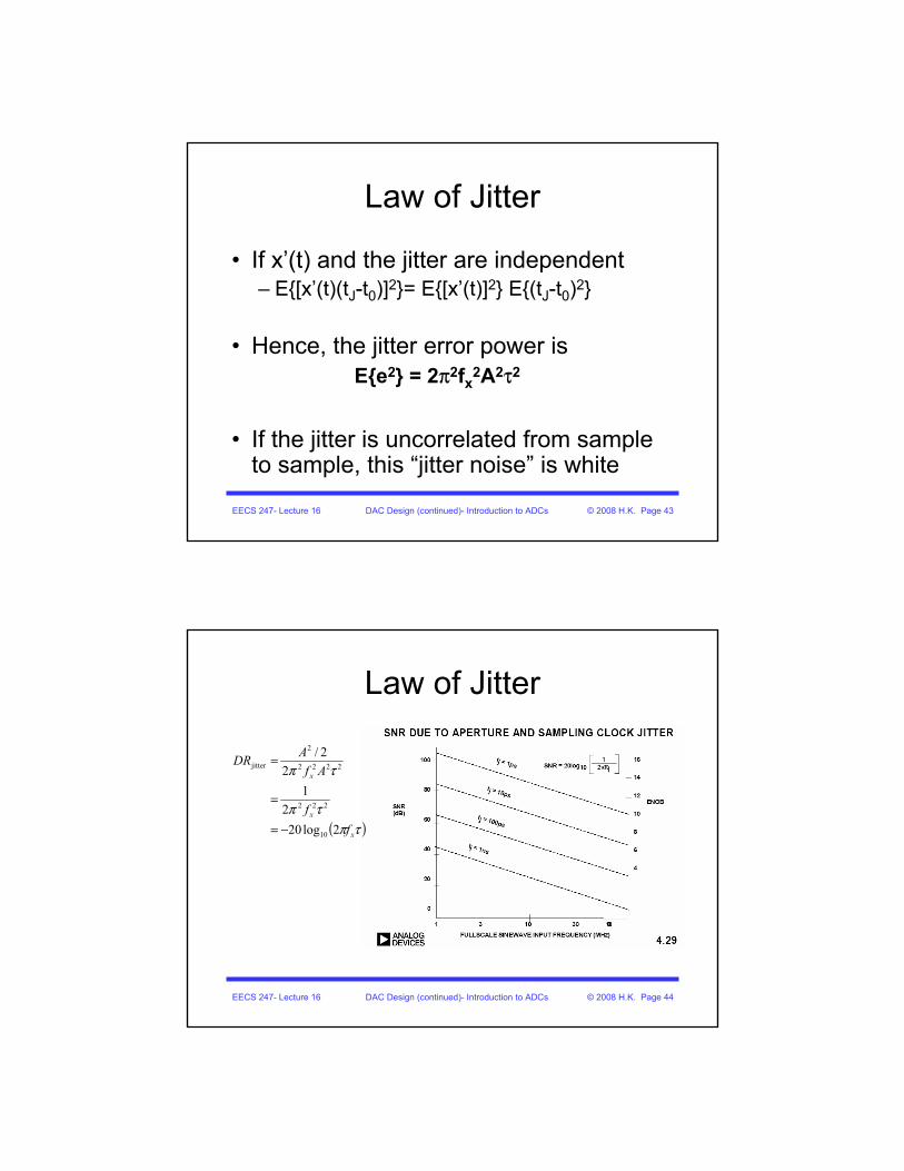
Law of Jitter
• The worst case looks pretty stringent …what about the “average”?
• Let’s calculate the mean squared jitter error (variance)• If we’re sampling a sinusoidal signal
x(t) = Asin(2πfxt), then– x’(t) = 2πfxAcos(2πfxt)– E{[x’(t)]2} = 2π2fx2A2
• Assume the jitter has variance E{(tJ-t0)2} = τ2
EECS 247- Lecture 16 DAC Design (continued)- Introduction to ADCs © 2008 H.K. Page 43
Law of Jitter
• If x’(t) and the jitter are independent– E{[x’(t)(tJ-t0)]2}= E{[x’(t)]2} E{(tJ-t0)2}
• Hence, the jitter error power is
• If the jitter is uncorrelated from sample to sample, this “jitter noise” is white
E{e2} = 2π2fx2A2τ2
EECS 247- Lecture 16 DAC Design (continued)- Introduction to ADCs © 2008 H.K. Page 44
Law of Jitter
( )τπτπ
τπ
x
x
x
ff
AfADR
2log202
12
2/
10
222
2222
2
jitter
−=
=
=
EECS 247- Lecture 16 DAC Design (continued)- Introduction to ADCs © 2008 H.K. Page 45
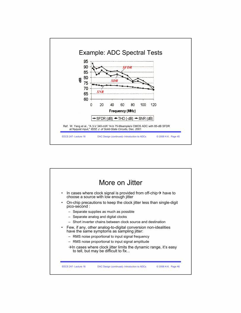
Example: ADC Spectral Tests
SFDR
SDR
SNR
Ref: W. Yang et al., "A 3-V 340-mW 14-b 75-Msample/s CMOS ADC with 85-dB SFDR at Nyquist input," IEEE J. of Solid-State Circuits, Dec. 2001
EECS 247- Lecture 16 DAC Design (continued)- Introduction to ADCs © 2008 H.K. Page 46
More on Jitter• In cases where clock signal is provided from off-chip have to
choose a source with low enough jitter• On-chip precautions to keep the clock jitter less than single-digit
pico-second :– Separate supplies as much as possible– Separate analog and digital clocks– Short inverter chains between clock source and destination
• Few, if any, other analog-to-digital conversion non-idealities have the same symptoms as sampling jitter:– RMS noise proportional to input signal frequency– RMS noise proportional to input signal amplitude
In cases where clock jitter limits the dynamic range, it’s easy to tell, but may be difficult to fix...
EECS 247- Lecture 16 DAC Design (continued)- Introduction to ADCs © 2008 H.K. Page 47
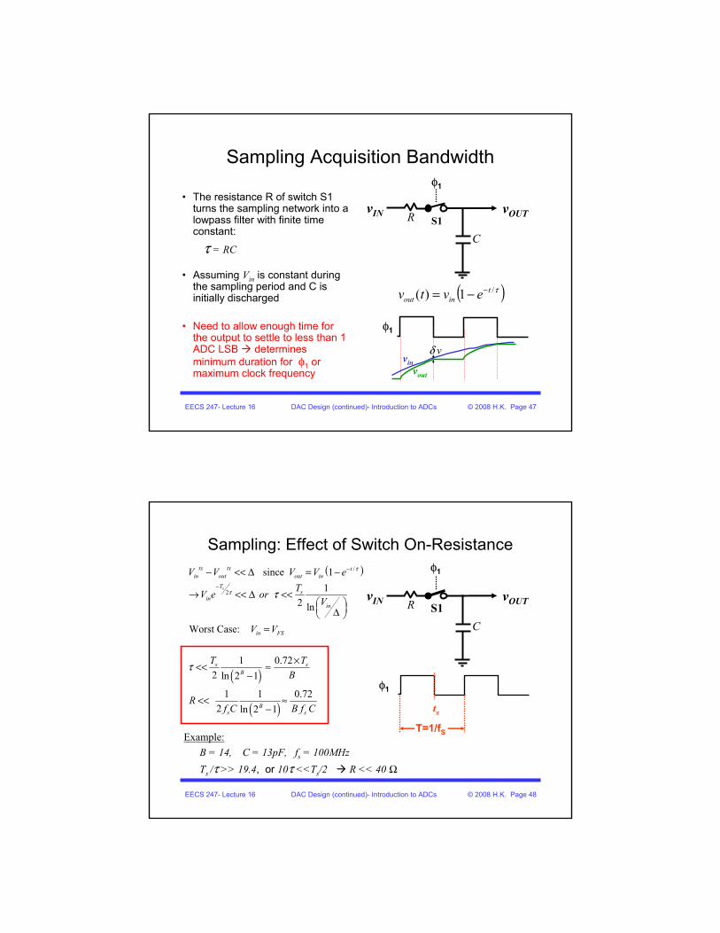
Sampling Acquisition Bandwidth
• The resistance R of switch S1 turns the sampling network into a lowpass filter with finite time constant:
τ = RC
• Assuming Vin is constant during the sampling period and C is initially discharged
• Need to allow enough time for the output to settle to less than 1 ADC LSB determines minimum duration for φ1 or maximum clock frequency
vIN vOUT
CS1
φ1
R
( )τ/1)( tinout evtv −−=
φ1
vinvout
δ v
EECS 247- Lecture 16 DAC Design (continued)- Introduction to ADCs © 2008 H.K. Page 48
Sampling: Effect of Switch On-Resistance
Example:B = 14, C = 13pF, fs = 100MHzTs /τ >> 19.4, or 10τ <<Ts/2 R << 40 Ω
φ1
T=1/fS
tx
( )
( )
( )
/
2
since 11
2 ln
Worst Case:
1 0.722 ln 2 1
1 1 0.722 ln 2 1
s
tx tx tin out out in
Ts
inin
in FS
s sB
Bs s
V V V V eTV e or
V
V V
T TB
Rf C B f C
τ
τ τ
τ
−
−
− << Δ = −
→ << Δ <<⎛ ⎞⎜ ⎟Δ⎝ ⎠
=
×<< ≈−
<< ≈−
vIN vOUT
CS1
φ1
R

EECS 247- Lecture 16 DAC Design (continued)- Introduction to ADCs © 2008 H.K. Page 49
Switch On-Resistance
( ) ( )
( )
( )( )
0
1,2
1 1
1Let us call @ =0
1
DS
D triodeDSD triode ox GS TH DS
ON DS V
ON
ox GS th ox DD th in
in o o
ox DD th
oON
in
DD th
dIVWI C V V VL R dV
R W WC V V C V V VL L
R V R then R WC V VL
RR VV V
μ
μ μ
μ
→
⎛ ⎞= − − ≅⎜ ⎟⎝ ⎠
= =− − −
=−
=− −
Switch MOS operating in triode mode:
Vin
CM1
φ1 VDDVGS =VDD - Vin
EECS 247- Lecture 16 DAC Design (continued)- Introduction to ADCs © 2008 H.K. Page 50
Sampling Distortion
in
DD th
outT V12 V V
in
v
v 1 e τ
⎛ ⎞− −⎜ ⎟⎜ ⎟−⎝ ⎠
=⎛ ⎞⎜ ⎟−⎜ ⎟⎜ ⎟⎝ ⎠
Simulated 10-Bit ADC &Ts/2 = 5τVDD – Vth = 2V VFS = 1VSampling Switch modeled:
Results in HD2=-41dBFS & HD3=-51.4dBFS
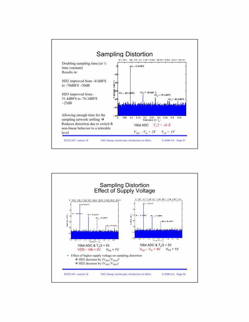
EECS 247- Lecture 16 DAC Design (continued)- Introduction to ADCs © 2008 H.K. Page 51
Sampling Distortion
10bit ADC Ts/2 = 10 τVDD – Vth = 2V VFS = 1V
Doubling sampling time (or ½time constant)Results in:
HD2 improved from -41dBFS to -70dBFS ~30dB
HD3 improved from -51.4dBFS to -76.3dBFS ~25dB
Allowing enough time for the sampling network settling Reduces distortion due to switch R non-linear behavior to a tolerable level
EECS 247- Lecture 16 DAC Design (continued)- Introduction to ADCs © 2008 H.K. Page 52
Sampling DistortionEffect of Supply Voltage
10bit ADC & Ts/2 = 5τVDD – Vth = 2V VFS = 1V
• Effect of higher supply voltage on sampling distortionHD3 decrease by (VDD1/VDD2)2
HD2 decrease by (VDD1/VDD2)
10bit ADC & Ts/2 = 5τVDD – Vth = 4V VFS = 1V
EECS 247- Lecture 16 DAC Design (continued)- Introduction to ADCs © 2008 H.K. Page 53
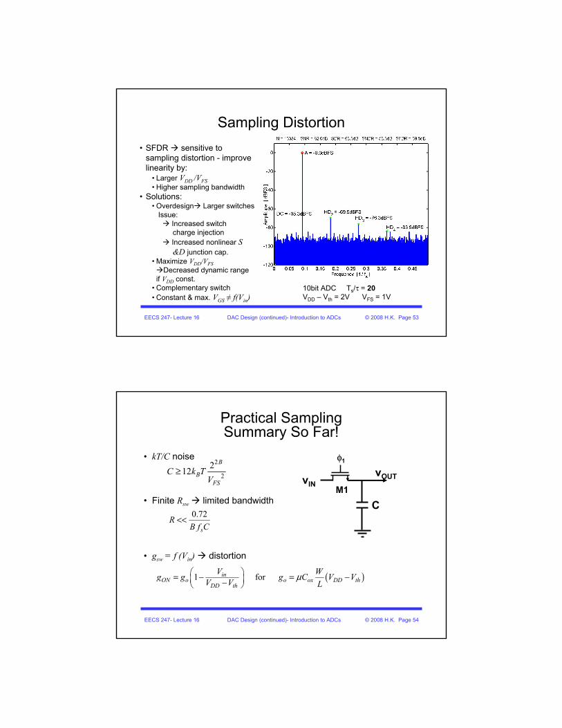
Sampling Distortion
10bit ADC Ts/τ = 20VDD – Vth = 2V VFS = 1V
• SFDR sensitive to sampling distortion - improve linearity by:
• Larger VDD /VFS• Higher sampling bandwidth
• Solutions:• Overdesign Larger switches
Issue: Increased switchcharge injectionIncreased nonlinear S &D junction cap.
• Maximize VDD/VFSDecreased dynamic range
if VDD const.• Complementary switch• Constant & max. VGS ≠ f(Vin)
EECS 247- Lecture 16 DAC Design (continued)- Introduction to ADCs © 2008 H.K. Page 54
Practical SamplingSummary So Far!
2
2212
B
BFS
C k TV
≥
( )1 for inON o o ox DD th
DD th
WVg g g C V VV V Lμ⎛ ⎞= − = −⎜ ⎟−⎝ ⎠
0.72
sR
B f C<<
• kT/C noise
• Finite Rsw limited bandwidth
• gsw = f (Vin) distortion
vINvOUT
CM1
φ1
EECS 247- Lecture 16 DAC Design (continued)- Introduction to ADCs © 2008 H.K. Page 55
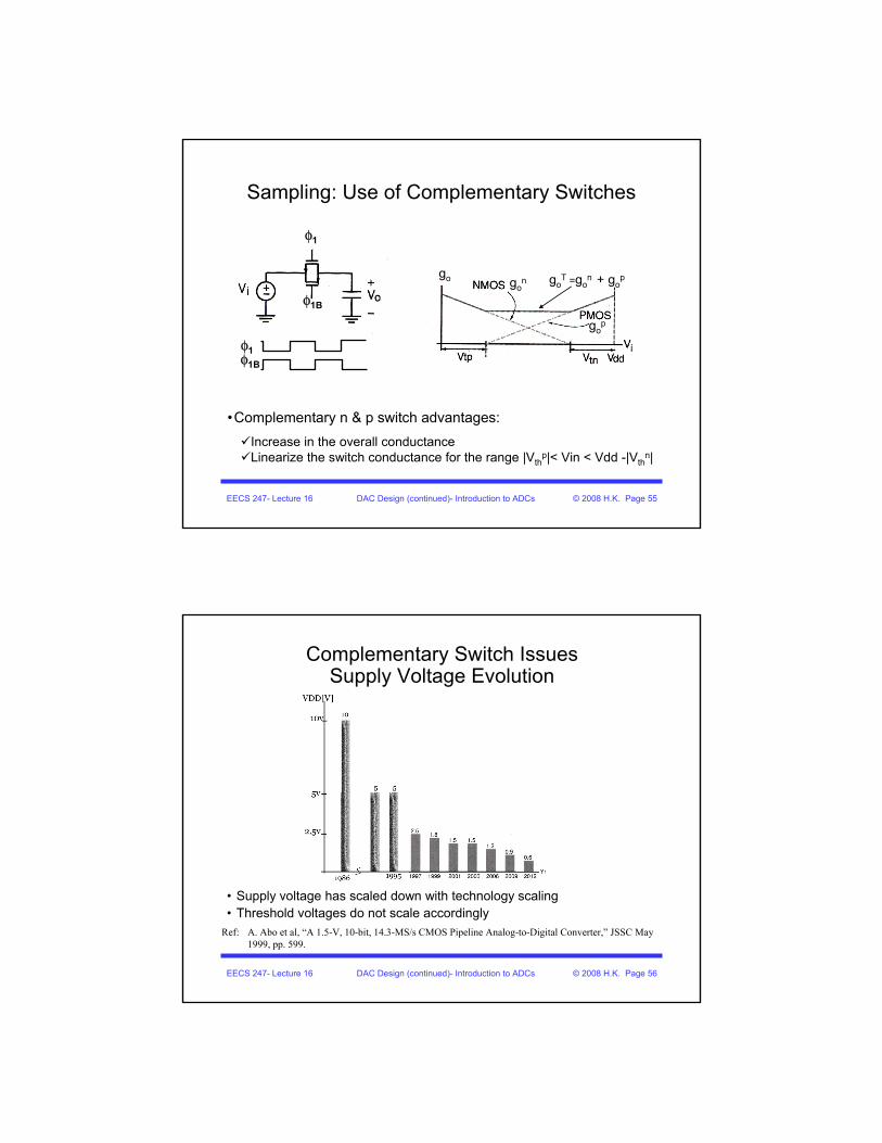
Sampling: Use of Complementary Switches
φ1φ1B
φ1
φ1B
gon
gop
goT =go
n + gopgo
•Complementary n & p switch advantages:Increase in the overall conductanceLinearize the switch conductance for the range |Vth
p|< Vin < Vdd -|Vthn|
EECS 247- Lecture 16 DAC Design (continued)- Introduction to ADCs © 2008 H.K. Page 56
Complementary Switch IssuesSupply Voltage Evolution
• Supply voltage has scaled down with technology scaling• Threshold voltages do not scale accordingly
Ref: A. Abo et al, “A 1.5-V, 10-bit, 14.3-MS/s CMOS Pipeline Analog-to-Digital Converter,” JSSC May 1999, pp. 599.
EECS 247- Lecture 16 DAC Design (continued)- Introduction to ADCs © 2008 H.K. Page 57
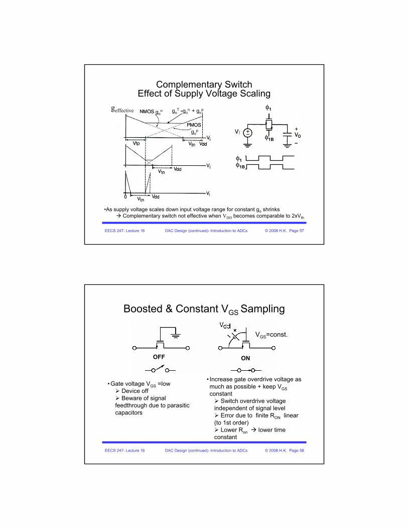
Complementary SwitchEffect of Supply Voltage Scaling
gon
gop
goT =go
n + gopgeffective
•As supply voltage scales down input voltage range for constant go shrinksComplementary switch not effective when VDD becomes comparable to 2xVth
φ1φ1B
φ1
φ1B
EECS 247- Lecture 16 DAC Design (continued)- Introduction to ADCs © 2008 H.K. Page 58
Boosted & Constant VGS Sampling
VGS=const.
OFF ON
• Increase gate overdrive voltage as much as possible + keep VGSconstant
Switch overdrive voltage independent of signal level
Error due to finite RON linear (to 1st order)
Lower Ron lower time constant
• Gate voltage VGS =lowDevice offBeware of signal
feedthrough due to parasitic capacitors
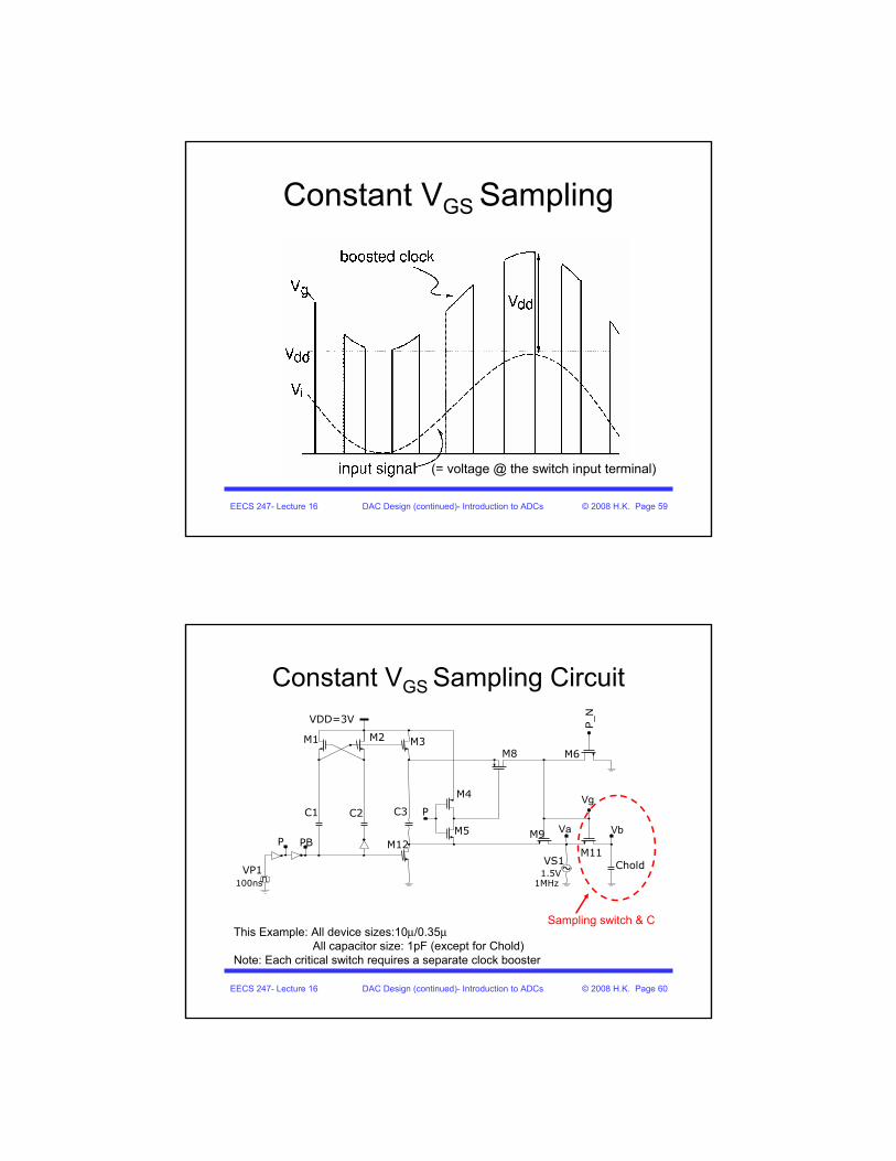
EECS 247- Lecture 16 DAC Design (continued)- Introduction to ADCs © 2008 H.K. Page 59
Constant VGS Sampling
(= voltage @ the switch input terminal)
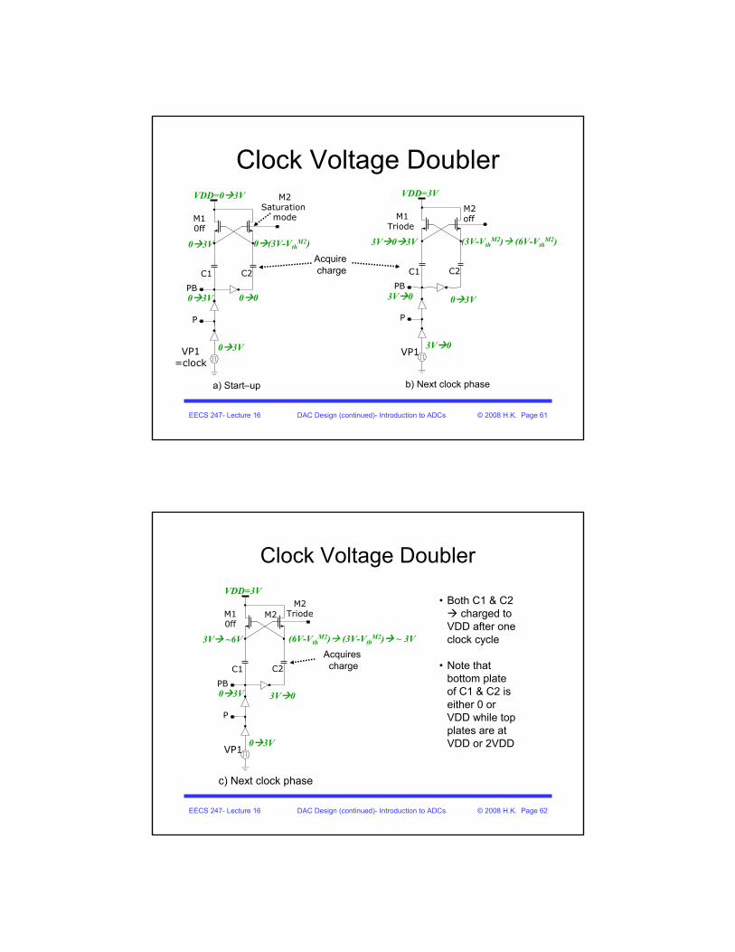
EECS 247- Lecture 16 DAC Design (continued)- Introduction to ADCs © 2008 H.K. Page 60
Constant VGS Sampling Circuit
VP1100ns
M12
M8
M9
M6
M11VS1
1.5V1MHz
Chold
P
C1 C2
M1 M2
VDD=3V
M3
C3
M5
M4
P
This Example: All device sizes:10μ/0.35μAll capacitor size: 1pF (except for Chold)
Note: Each critical switch requires a separate clock booster
P_N
Vg
Va Vb
Sampling switch & C
PB
EECS 247- Lecture 16 DAC Design (continued)- Introduction to ADCs © 2008 H.K. Page 61
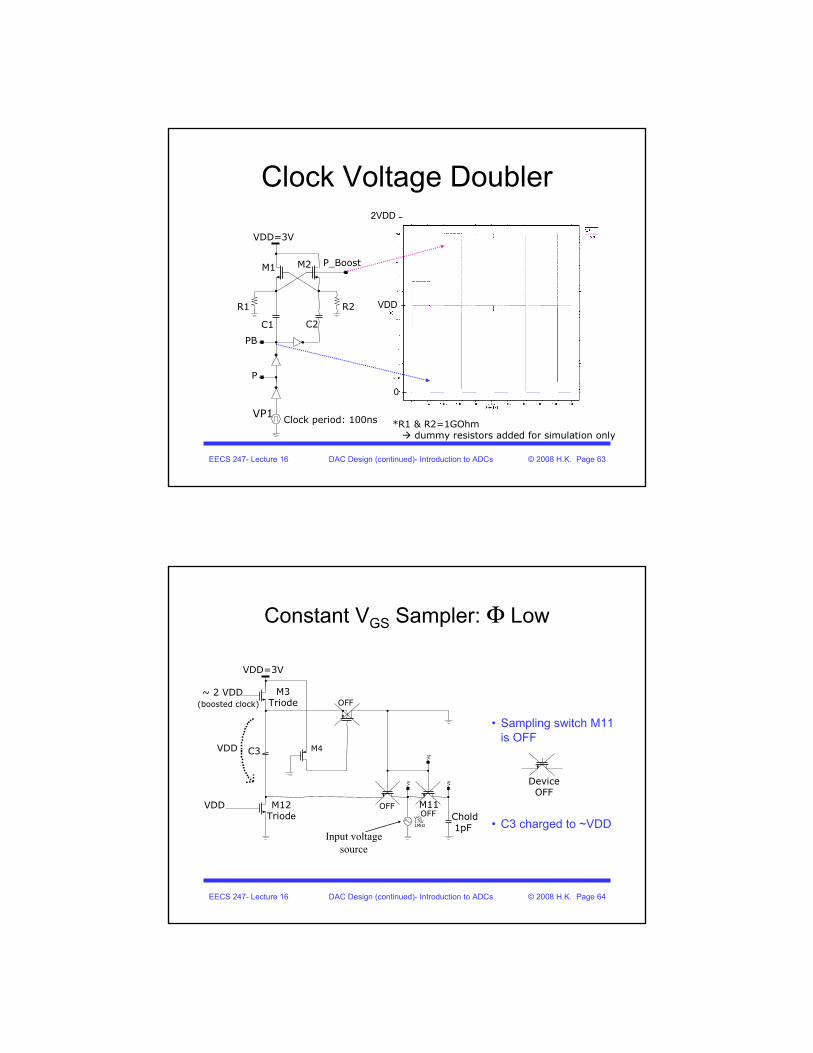
Clock Voltage Doubler
C1 C2
M10ff
M2Saturation
mode
VP1=clock
PB
VDD=0 3V
P
a) Start–up
0 3V
0 3V 0 0
0 3V 0 (3V-VthM2)
Acquire charge C1 C2
M1Triode
M2off
VP1
PB
VDD=3V
P
3V 0
3V 0
3V 0 3V (3V-VthM2) (6V-Vth
M2)
b) Next clock phase
0 3V
EECS 247- Lecture 16 DAC Design (continued)- Introduction to ADCs © 2008 H.K. Page 62
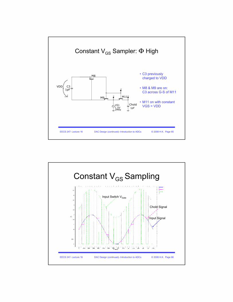
Clock Voltage Doubler
C1 C2
M10ff
M2
VP1
PB
VDD=3V
P
0 3V
0 3V
3V ~6V
3V 0
c) Next clock phase
(6V-VthM2) (3V-Vth
M2) ~ 3V
M2Triode
Acquires charge
• Both C1 & C2 charged to
VDD after one clock cycle
• Note that bottom plate of C1 & C2 is either 0 or VDD while top plates are at VDD or 2VDD
EECS 247- Lecture 16 DAC Design (continued)- Introduction to ADCs © 2008 H.K. Page 63
Clock Voltage Doubler
C1 C2
M1 M2
VP1Clock period: 100ns
PB
P_Boost
VDD
2VDD
0
VDD=3V
R1 R2
*R1 & R2=1GOhmdummy resistors added for simulation only
P
EECS 247- Lecture 16 DAC Design (continued)- Introduction to ADCs © 2008 H.K. Page 64
Constant VGS Sampler: Φ Low
• Sampling switch M11 is OFF
• C3 charged to ~VDDInput voltage
source
M3Triode
C3
M12Triode
M4
OFF
VS11.5V1MHz
Chold1pF
~ 2 VDD(boosted clock)
VDD
VDD
OFF M11OFF
DeviceOFF
VDD=3V
EECS 247- Lecture 16 DAC Design (continued)- Introduction to ADCs © 2008 H.K. Page 65
Constant VGS Sampler: Φ High
• C3 previously charged to VDD
• M8 & M9 are on:C3 across G-S of M11
• M11 on with constant VGS = VDD
C31pF
M8
M9 M11
VS11.5V1MHz
Chold1pF
VDD
EECS 247- Lecture 16 DAC Design (continued)- Introduction to ADCs © 2008 H.K. Page 66
Constant VGS Sampling
Input Switch VGate
Input Signal
Chold Signal
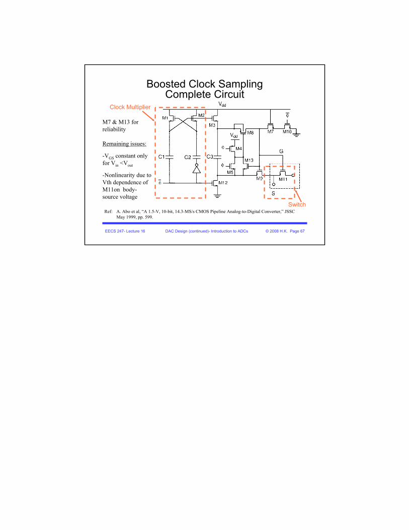
EECS 247- Lecture 16 DAC Design (continued)- Introduction to ADCs © 2008 H.K. Page 67
Boosted Clock Sampling Complete Circuit
Ref: A. Abo et al, “A 1.5-V, 10-bit, 14.3-MS/s CMOS Pipeline Analog-to-Digital Converter,” JSSC May 1999, pp. 599.
Clock Multiplier
Switch
M7 & M13 for reliability
Remaining issues:
-VGS constant only for Vin <Vout
-Nonlinearity due to Vth dependence of M11on body-source voltage