Embed Size (px)
Citation preview
1
UNESCO-NIGERIA TECHNICAL &
VOCATIONAL EDUCATION
REVITALISATION PROJECT-PHASE II
YEAR II- SEMESTER III
THEORY
Version 1: December 2008
NATIONAL DIPLOMA IN
ELECTRICAL ENGINEERING TECHNOLOGY
ELECTRICAL CIRCUITS (I)
COURSE CODE: EEC 239
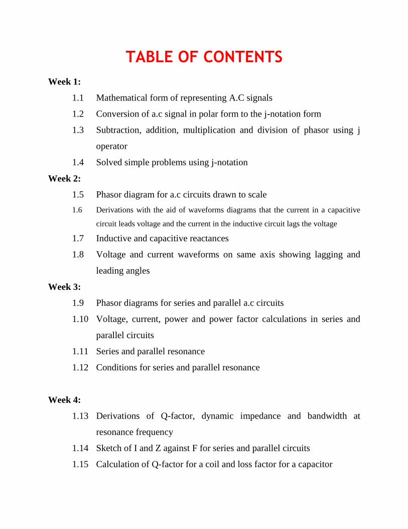
TABLE OF CONTENTS
Week 1:
1.1 Mathematical form of representing A.C signals
1.2 Conversion of a.c signal in polar form to the j-notation form
1.3 Subtraction, addition, multiplication and division of phasor using j
operator
1.4 Solved simple problems using j-notation
Week 2:
1.5 Phasor diagram for a.c circuits drawn to scale
1.6 Derivations with the aid of waveforms diagrams that the current in a capacitive
circuit leads voltage and the current in the inductive circuit lags the voltage
1.7 Inductive and capacitive reactances
1.8 Voltage and current waveforms on same axis showing lagging and
leading angles
Week 3:
1.9 Phasor diagrams for series and parallel a.c circuits
1.10 Voltage, current, power and power factor calculations in series and
parallel circuits
1.11 Series and parallel resonance
1.12 Conditions for series and parallel resonance
Week 4:
1.13 Derivations of Q-factor, dynamic impedance and bandwidth at
resonance frequency
1.14 Sketch of I and Z against F for series and parallel circuits
1.15 Calculation of Q-factor for a coil and loss factor for a capacitor
1.16 Bandwidth
1.17 Problems involving bandwidth and circuits Q-factor
Week 5:
2.1 Terms used in electric networks
WEEK 6:
2.2 Basic principles of mesh circuit analysis
2.3 Solved problems on mesh circuit analysis
Week 7:
2.4 Basic principles of nodal analysis
2.5 solved problems on nodal analysis
Week 8:
3.1 Reduction of a complex network to it series or parallel equivalent
3.2 Identification of star and delta networks
Week 9:
3.3 Derivation of formulae for the transformation of a delta to a star
network and vice versa
3.4 solved problems on delta/star transformation
Week 10:
3.5 Duality principles
3.6 Duality between resistance, conductance, inductance, capacitance,
voltage and current
Week 11:
3.7 Duality of a network
3.8 Solved network problems using duality principles
Week 12:
4.1 Thevenin’s theorem
4.2 Basic principles of Thevenin’s theorem
4.3 Solved problems on simple network using Thevenin’s theorem
4.4 Solved problems involving repeated used of Thevenin’s theorem
Week 13:
4.5 Norton’s theorem
4.6 Basic principles of Norton’s theorem
4.7 Comparison of Norton’s theorem with Thevenin’s theorem
4.8 Solved problems using Norton’s theorem
Week 14:
4.9 Millman’s theorem
4.10 Basic principles of Millman’s theorem
4.11 Solved network problems using Millman’s theorem
Week 15:
4.12 Reciprocity Theorem
4.13 Basic principles of Reciprocity theorem
4.14 Solved problems using Reciprocity theorems
A.C THEORY Week 1
1
At the end of this week, the students are expected to:
State different mathematical forms of representing a.c signals
Convert a.c signal in polar form to the j-notation
Subtract, add, multiply and divide phasor using j-operator
Solve simple problems using j-notation
1.1 MATHEMATICAL FORMS OF REPRESENTING A.C SIGNALS
Generally, A.C signal may be represented in the following mathematical form;
a) Trigonometric form, Z = r (Cos + sin ) (1.1)
b) Polar form, Z = r (1.2)
c) J – notation form, Z = x+jy (1.3)
1.2 CONVERSION OF A.C SIGNAL IN POLAR FORM TO THE
j – NOTATION FORM
Example 1.1: Express 18-56.3 in j – notation form
Solution:
Step I: Make a sketch as shown on fig 1.1 to measure = -56.30 with respect to the real axis and r =
OA = 18
Step II: Find x using trigonometric ratio,
Cos = x/18
i.e x = 18 cos = 18 Cos (-56.30)
x 10
Step III: Find y using trigonometric ratio
Sin = Y/18
i.e y = 18 sin = sin (-56.3O)
y -15
Step IV: finally obtain the required result as x + jy = 10 – j15
Example 1.2: Express 553.1o in j – notation form
Solution:
Step I: Make a sketch as shown on fig 1.2 to measure = 53.10 with respect to the real axis and r =
OA = 5
Step II: Find x using trigonometric ratio
18 A
Re
B x O
y
N
j
Fig 1.1
= -56.30
A.C THEORY Week 1
2
Cos = x/5
i.e x = 5 cos = 5 Cos (53.10)
x 3
Step III: Find y using trigonometric ratio
Sin = Y/5
i.e y = 5 sin = sin (53.1O)
y 4
Step IV: finally obtain the required result as x + jy = 3 – j4
1.3 SUBTRACTION, ADDITION, MULTIPLICATION AND DIVISION OF
PHASOR USING j- OPERATOR.
1.3.1 Addition/Subtraction of Phasor
The most convenient way to add or subtract phasor is to first convert them to j – notation form, if
they are in polar form. Once the phasor are in j – notation form, the real (x) components and the
imaginary (y) components can be algebraically added or subtracted, as may be required. The answer
(the sum or difference) can be left in j – notation form or it can be converted back to polar form if
desired.
If two phasor are Z1 and a +jb and Z2 = c+jd, then addition of phasor gives: Z1 + Z2 = (a+jb) + (c+jd)
= (a+c) + j(b+d)
Subtraction of phasor gives: Z1 – Z2 = (a-c) + j(b-d)
Example 1.3: If V1 = -10 + j20 and V2 = 20 +j30 , find the sum of V1 and V2, express the result in
polar form.
Solution
V1 = -10+j20
V2 = 20 + j30
V3 = V1 + V2 = -10+ 20+j20 + j30 = 10 +j50
Finally, V3 = 102+50
2 Tan
-1 (
50/10) = 5178.7
0
A
Re B
x
y
N
Fig 1.2
= 53.10
S
A.C THEORY Week 1
3
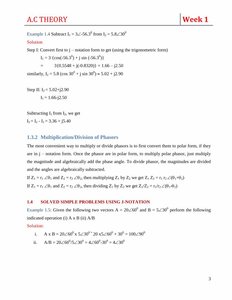
Example 1.4 Subtract I1 = 3-56.30 from I2 = 5.830
0
Solution
Step I: Convert first to j – notation form to get (using the trigonometric form)
I1 = 3 cos(-56.30) + j sin (-56.3
0)
= 30.5548 + j(-0.8320) = 1.66 – j2.50
similarly, I2 = 5.8 (cos 300 + j sin 30
0) 5.02 + j2.90
Step II: I2 = 5.02+j2.90
I1 = 1.66-j2.50
Subtracting I1 from I2, we get
I3 = I2 - I1 = 3.36 + j5.40
1.3.2 Multiplication/Division of Phasors
The most convenient way to multiply or divide phasors is to first convert them to polar form, if they
are in j – notation form. Once the phasor are in polar form, to multiply polar phasor, just multiply
the magnitude and algebraically add the phase angle. To divide phasor, the magnitudes are divided
and the angles are algebraically subtracted.
If Z1 = r1 1 and Z2 = r2 2, then multiplying Z1 by Z2 we get Z1 Z2 = r1 r2 (1+2)
If Z1 = r1 1 and Z2 = r2 2, then dividing Z1 by Z2 we get Z1/Z2 = r1/r2 (1-2)
1.4 SOLVED SIMPLE PROBLEMS USING J-NOTATION
Example 1.5: Given the following two vectors A = 20600 and B = 530
0 perform the following
indicated operation (i) A x B (ii) A/B
Solution:
i. A x B = 20600
x 5300 =
20 x5600 + 30
0 = 10090
0
ii. A/B = 20600/530
0 = 460
0-30
0 = 430
0
A.C THEORY Week 1
4
Example 1.6: perform the following operation and the final result may be given in polar for; (8
+j6)x(-10-j7.5)
Solution
(8+j6)x(-10-j7.5)= -80-j60-j60-j245=-80+45-j120
= -35-j120 = (-35)2+ (-120)
2 tan
-1(120
/35) = 12573.70
A.C THEORY Week 2
5
At the end of this week, the students are expected to:
Draw to scale phasor diagram for a.c circuits
Show with the aid of waveforms diagrams that the current in a capacitor circuit leads voltage
and the current in the inductive circuit lags the voltage.
Distinguish between inductive and capacitive reactances.
Draw voltage and current waveforms on same axis to show lagging and leading angles.
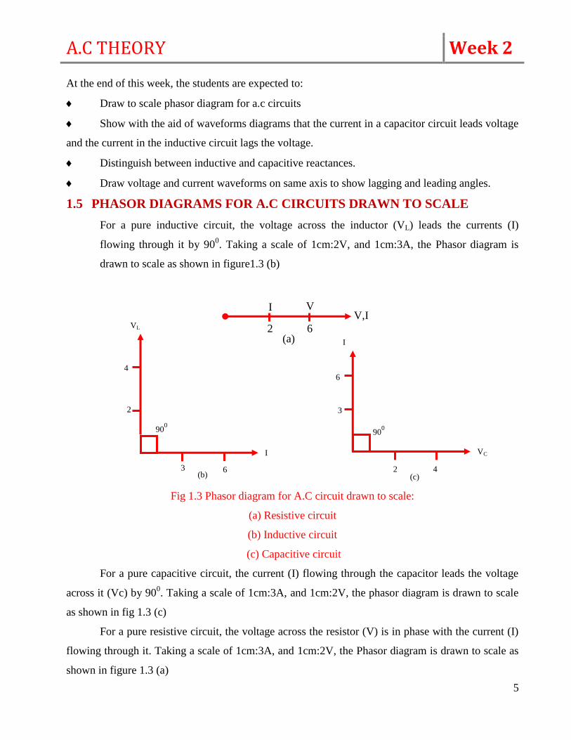
1.5 PHASOR DIAGRAMS FOR A.C CIRCUITS DRAWN TO SCALE
For a pure inductive circuit, the voltage across the inductor (VL) leads the currents (I)
flowing through it by 900. Taking a scale of 1cm:2V, and 1cm:3A, the Phasor diagram is
drawn to scale as shown in figure1.3 (b)
Fig 1.3 Phasor diagram for A.C circuit drawn to scale:
(a) Resistive circuit
(b) Inductive circuit
(c) Capacitive circuit
For a pure capacitive circuit, the current (I) flowing through the capacitor leads the voltage
across it (Vc) by 900. Taking a scale of 1cm:3A, and 1cm:2V, the phasor diagram is drawn to scale
as shown in fig 1.3 (c)
For a pure resistive circuit, the voltage across the resistor (V) is in phase with the current (I)
flowing through it. Taking a scale of 1cm:3A, and 1cm:2V, the Phasor diagram is drawn to scale as
shown in figure 1.3 (a)
I V V,I
2 6 (a)
900
6
I
VL
4
(b)
2
3 4 2
900
VC
I
6
(c)
3
A.C THEORY Week 2
6
1.6 DERIVATIONS WITH THE AID OF WAVEFORMS DIAGRAMS
THAT THE CURRENT IN A CAPACITIVE CIRCUIT LEADS
VOLTAGE AND THE CURRENT IN THE INDUCTIVE CIRCUIT
LAGS THE VOLTAGE
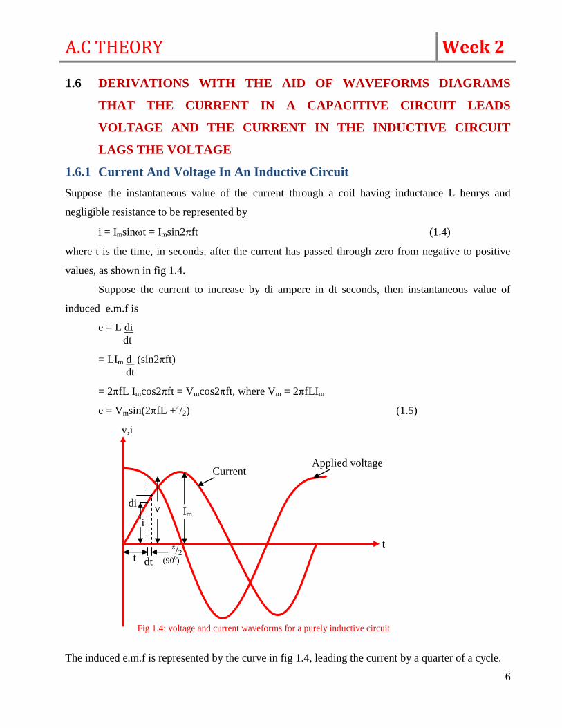
1.6.1 Current And Voltage In An Inductive Circuit
Suppose the instantaneous value of the current through a coil having inductance L henrys and
negligible resistance to be represented by
i = Imsint = Imsin2πft (1.4)
where t is the time, in seconds, after the current has passed through zero from negative to positive
values, as shown in fig 1.4.
Suppose the current to increase by di ampere in dt seconds, then instantaneous value of
induced e.m.f is
e = L di
dt
= LIm d (sin2πft)
dt
= 2πfL Imcos2πft = Vmcos2πft, where Vm = 2πfLIm
e = Vmsin(2πfL +π/2) (1.5)
The induced e.m.f is represented by the curve in fig 1.4, leading the current by a quarter of a cycle.
v,i
v
i
di Im
dt t (900)
π/2
Current Applied voltage
t
Fig 1.4: voltage and current waveforms for a purely inductive circuit
A.C THEORY Week 2
7
Since the resistance of the circuit is assumed negligible, the whole of the applied voltage is
equal to the induced e.m.f, therefore instantaneous value of applied voltage is
V = e
V = Vmsin(2πft + π/2) (1.6)
Comparism of expressions (1.4) and (1.6) shows that the applied voltage leads the current by
a quarter of a cycle.
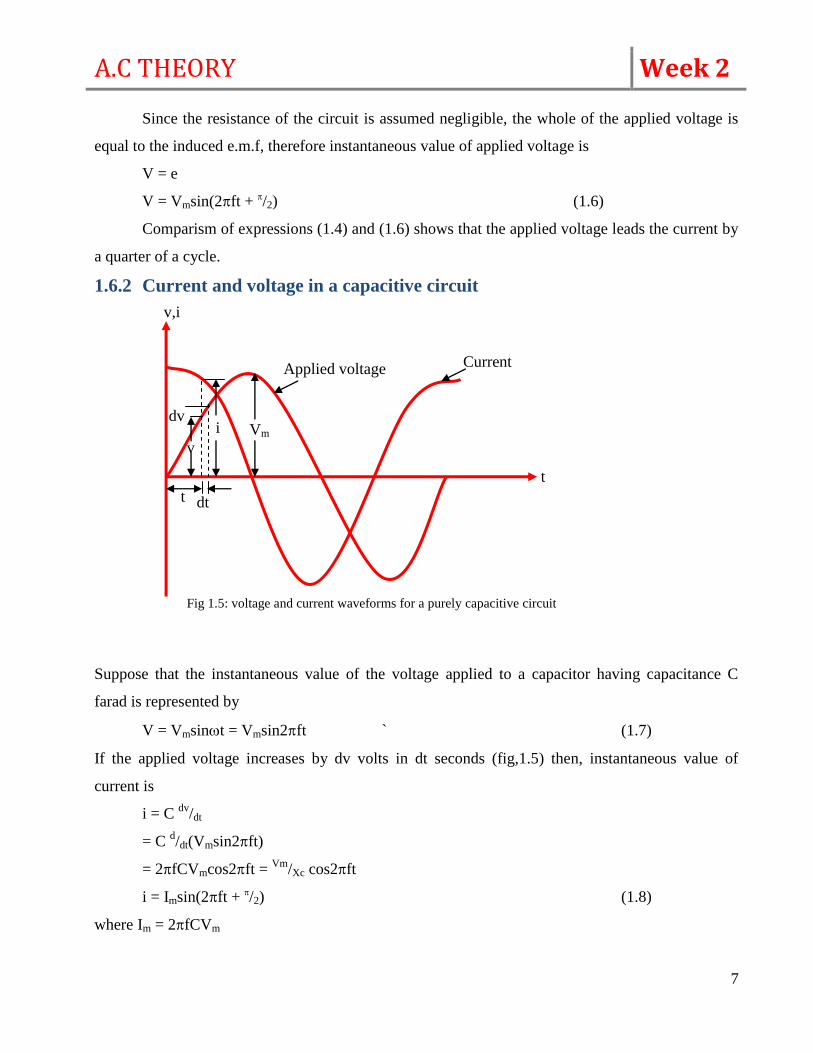
1.6.2 Current and voltage in a capacitive circuit
Suppose that the instantaneous value of the voltage applied to a capacitor having capacitance C
farad is represented by
V = Vmsint = Vmsin2πft ` (1.7)
If the applied voltage increases by dv volts in dt seconds (fig,1.5) then, instantaneous value of
current is
i = C dv
/dt
= C d/dt(Vmsin2πft)
= 2πfCVmcos2πft = Vm
/Xc cos2πft
i = Imsin(2πft + π/2) (1.8)
where Im = 2πfCVm
v,i
v
i dv
Vm
dt t
Current Applied voltage
t
Fig 1.5: voltage and current waveforms for a purely capacitive circuit
A.C THEORY Week 2
8
Comparism of expression (1.7) and (1.8) shows that the current leads the applied voltage by
a quarter of a cycle.
1.7 DISTINGUISH BETWEEN INDUCTIVE AND CAPACITIVE
REACTANCES
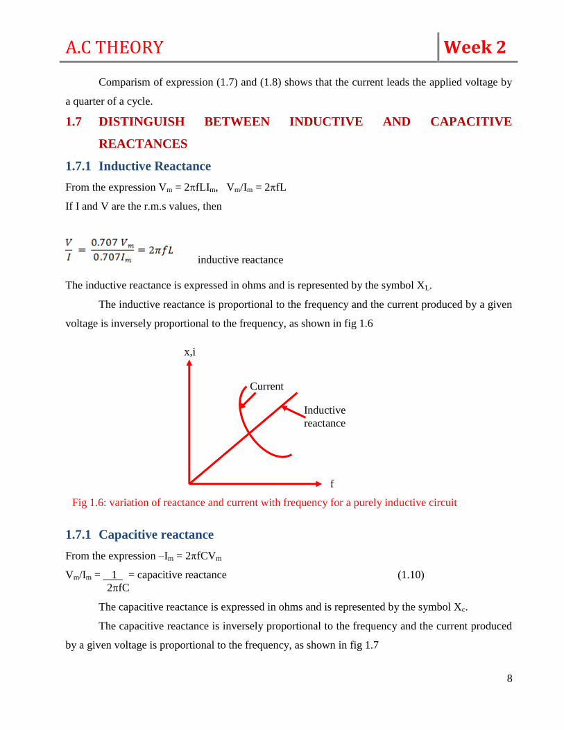
1.7.1 Inductive Reactance
From the expression Vm = 2πfLIm, Vm/Im = 2πfL
If I and V are the r.m.s values, then
inductive reactance
The inductive reactance is expressed in ohms and is represented by the symbol XL.
The inductive reactance is proportional to the frequency and the current produced by a given
voltage is inversely proportional to the frequency, as shown in fig 1.6
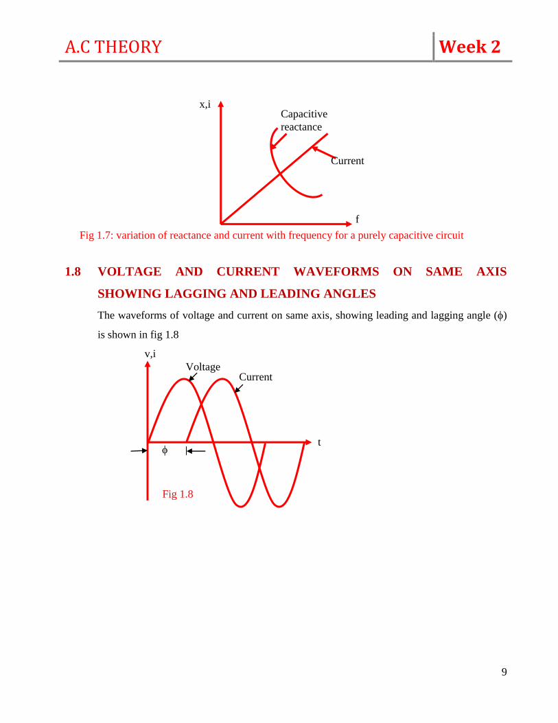
1.7.1 Capacitive reactance
From the expression –Im = 2πfCVm
Vm/Im = 1 = capacitive reactance (1.10)
2πfC
The capacitive reactance is expressed in ohms and is represented by the symbol Xc.
The capacitive reactance is inversely proportional to the frequency and the current produced
by a given voltage is proportional to the frequency, as shown in fig 1.7
f
Current
Inductive
reactance
x,i
Fig 1.6: variation of reactance and current with frequency for a purely inductive circuit
A.C THEORY Week 2
9
1.8 VOLTAGE AND CURRENT WAVEFORMS ON SAME AXIS
SHOWING LAGGING AND LEADING ANGLES
The waveforms of voltage and current on same axis, showing leading and lagging angle ()
is shown in fig 1.8
Current
Capacitive
reactance
f
x,i
Fig 1.7: variation of reactance and current with frequency for a purely capacitive circuit
Voltage Current
v,i
Fig 1.8
t
A.C THEORY Week 3
10
At the end of this week, the students are expected to:
Draw phasor diagram for series and parallel a.c circuits
Calculate voltage, current, power and power factor in series and parallel circuits
Explain series and parallel resonance
State conditions for series and parallel resonance
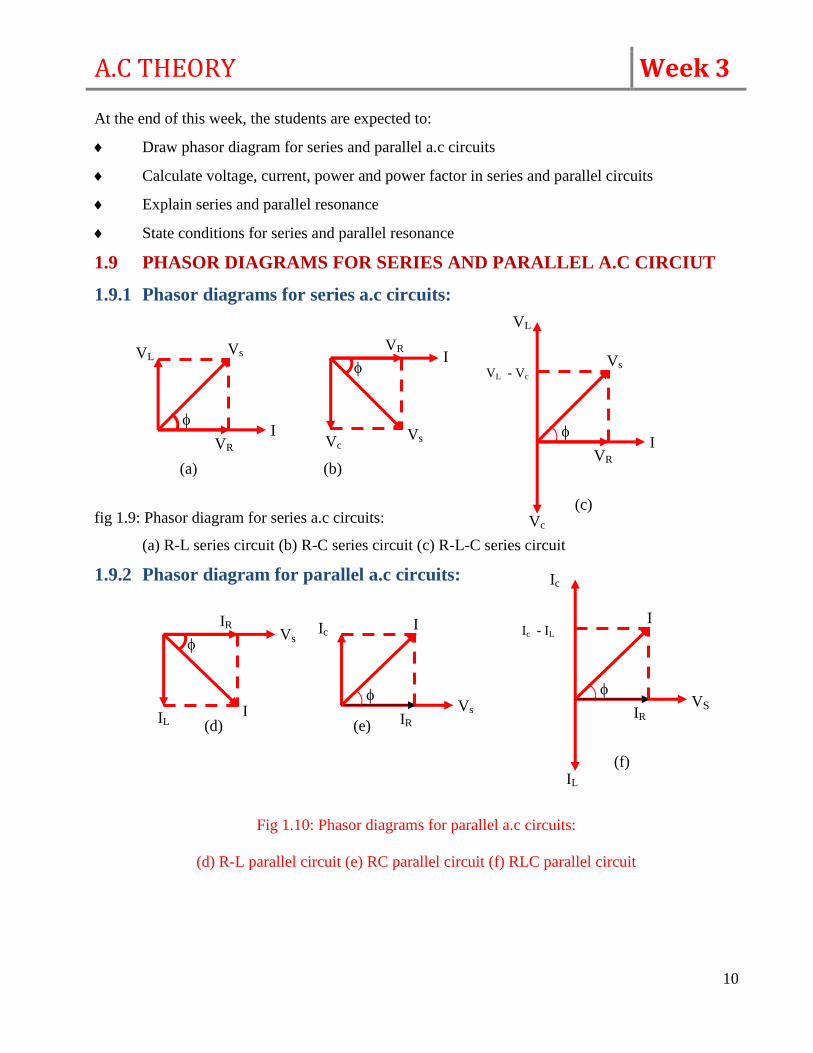
1.9 PHASOR DIAGRAMS FOR SERIES AND PARALLEL A.C CIRCIUT
1.9.1 Phasor diagrams for series a.c circuits:
fig 1.9: Phasor diagram for series a.c circuits:
(a) R-L series circuit (b) R-C series circuit (c) R-L-C series circuit
1.9.2 Phasor diagram for parallel a.c circuits:
Fig 1.10: Phasor diagrams for parallel a.c circuits:
(d) R-L parallel circuit (e) RC parallel circuit (f) RLC parallel circuit
I Vs VL
VR
I Vs
VR
Vc
(a) (b)
Vs
VL
VR
I
Vc
VL - Vc
(c)
I
IR
IL
Vs
(d)
I Ic
IR
Vs
(e)
I
Ic
IR
VS
IL
Ic - IL
(f)
A.C THEORY Week 3
11
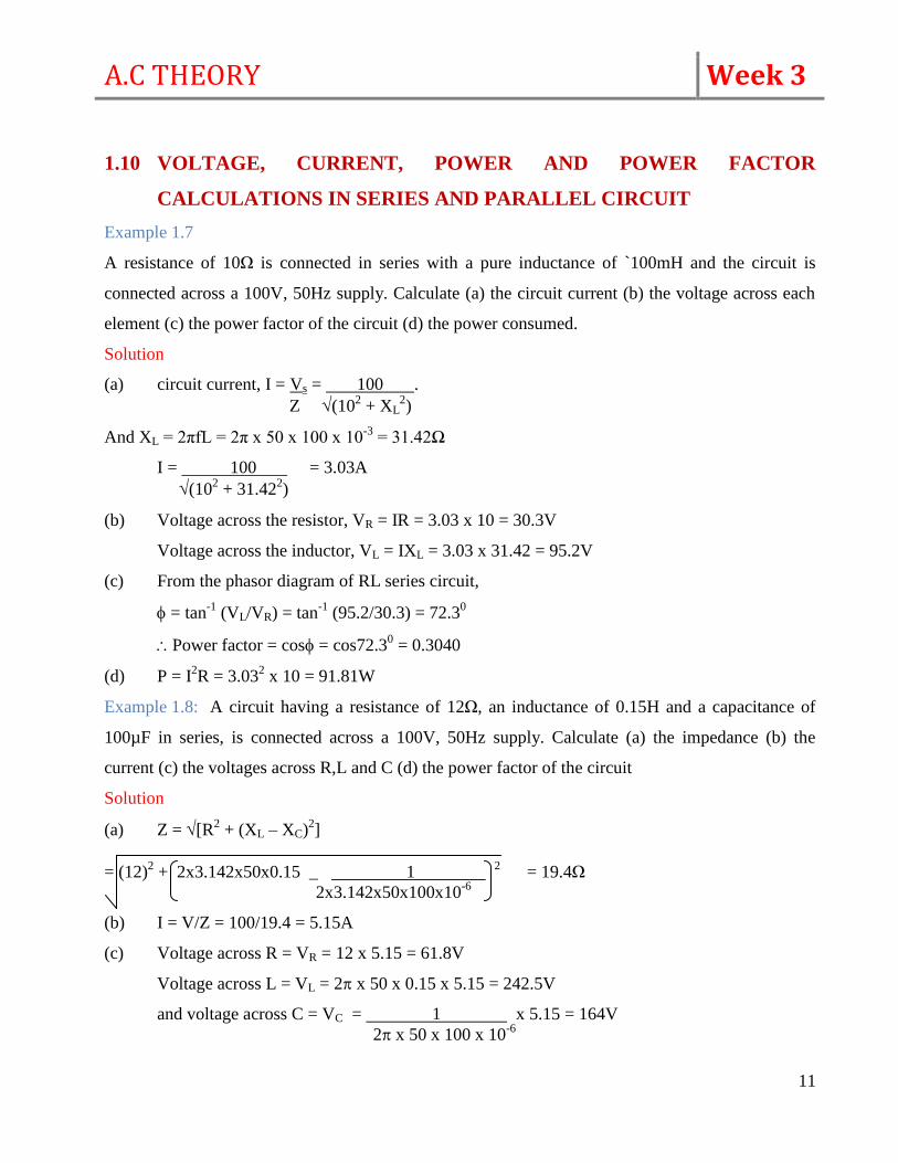
1.10 VOLTAGE, CURRENT, POWER AND POWER FACTOR
CALCULATIONS IN SERIES AND PARALLEL CIRCUIT
Example 1.7
A resistance of 10Ω is connected in series with a pure inductance of `100mH and the circuit is
connected across a 100V, 50Hz supply. Calculate (a) the circuit current (b) the voltage across each
element (c) the power factor of the circuit (d) the power consumed.
Solution
(a) circuit current, I = Vs = 100 .
Z (102 + XL
2)
And XL = 2πfL = 2π x 50 x 100 x 10-3
= 31.42Ω
I = 100 = 3.03A
(102 + 31.42
2)
(b) Voltage across the resistor, VR = IR = 3.03 x 10 = 30.3V
Voltage across the inductor, VL = IXL = 3.03 x 31.42 = 95.2V
(c) From the phasor diagram of RL series circuit,
= tan-1
(VL/VR) = tan-1
(95.2/30.3) = 72.30
Power factor = cos = cos72.30 = 0.3040
(d) P = I2R = 3.03
2 x 10 = 91.81W
Example 1.8: A circuit having a resistance of 12Ω, an inductance of 0.15H and a capacitance of
100µF in series, is connected across a 100V, 50Hz supply. Calculate (a) the impedance (b) the
current (c) the voltages across R,L and C (d) the power factor of the circuit
Solution
(a) Z = [R2 + (XL – XC)
2]
= (12)2 + 2x3.142x50x0.15 _ 1
2 = 19.4Ω
2x3.142x50x100x10-6
(b) I = V/Z = 100/19.4 = 5.15A
(c) Voltage across R = VR = 12 x 5.15 = 61.8V
Voltage across L = VL = 2π x 50 x 0.15 x 5.15 = 242.5V
and voltage across C = VC = 1 x 5.15 = 164V
2π x 50 x 100 x 10-6
A.C THEORY Week 3
12
(d) power factor = cos
Where = cos-1
(VR/VS) = cos-1
(61.8/100) = 51.80
P.f = cos51.8 = 0.6184
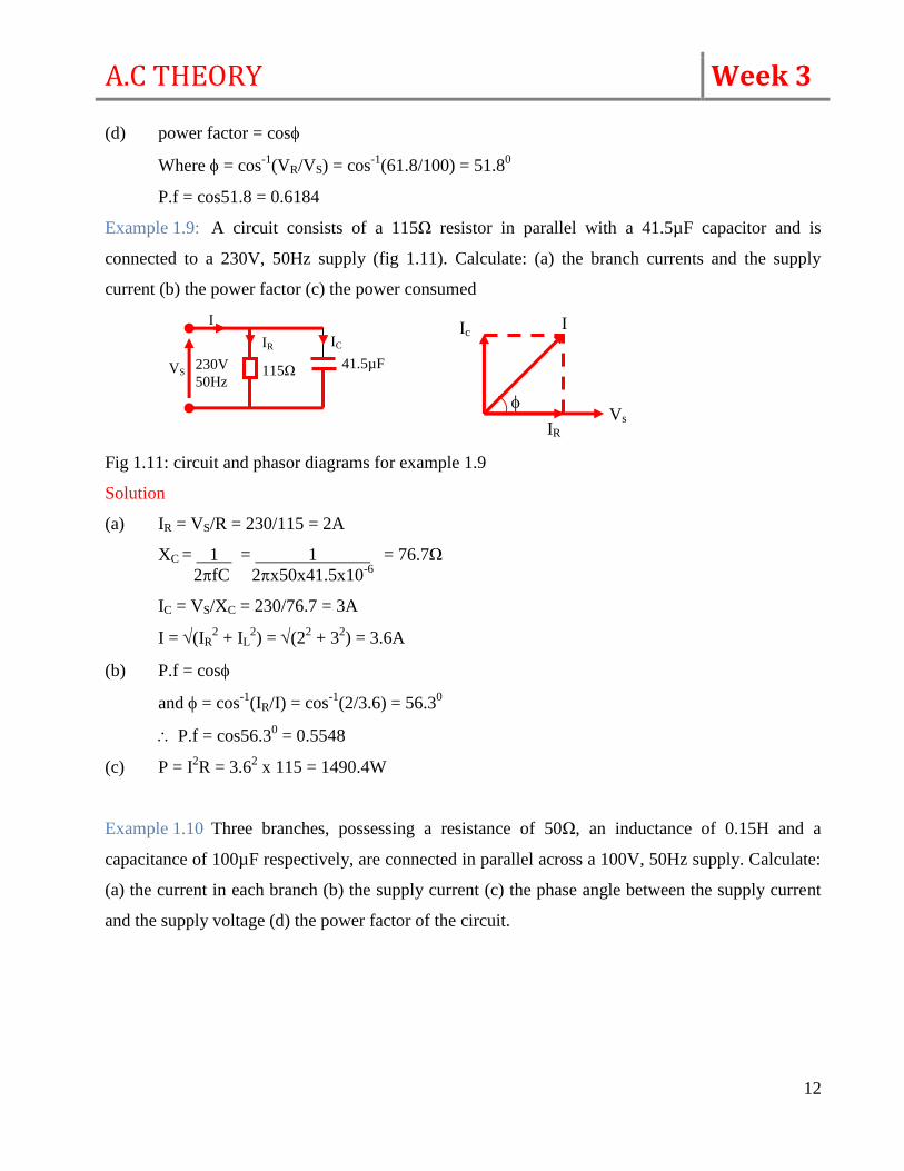
Example 1.9: A circuit consists of a 115Ω resistor in parallel with a 41.5µF capacitor and is
connected to a 230V, 50Hz supply (fig 1.11). Calculate: (a) the branch currents and the supply
current (b) the power factor (c) the power consumed
Fig 1.11: circuit and phasor diagrams for example 1.9
Solution
(a) IR = VS/R = 230/115 = 2A
XC = 1 = 1 = 76.7Ω
2πfC 2πx50x41.5x10-6
IC = VS/XC = 230/76.7 = 3A
I = (IR2 + IL
2) = (2
2 + 3
2) = 3.6A
(b) P.f = cos
and = cos-1
(IR/I) = cos-1
(2/3.6) = 56.30
P.f = cos56.30 = 0.5548
(c) P = I2R = 3.6
2 x 115 = 1490.4W
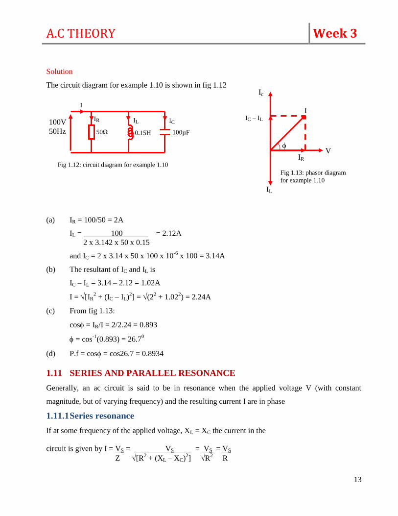
Example 1.10 Three branches, possessing a resistance of 50Ω, an inductance of 0.15H and a
capacitance of 100µF respectively, are connected in parallel across a 100V, 50Hz supply. Calculate:
(a) the current in each branch (b) the supply current (c) the phase angle between the supply current
and the supply voltage (d) the power factor of the circuit.
230V
50Hz VS 41.5µF
115Ω
IC IR
I
I Ic
IR
Vs
A.C THEORY Week 3
13
Solution
The circuit diagram for example 1.10 is shown in fig 1.12
(a) IR = 100/50 = 2A
IL = 100 = 2.12A
2 x 3.142 x 50 x 0.15
and IC = 2 x 3.14 x 50 x 100 x 10-6
x 100 = 3.14A
(b) The resultant of IC and IL is
IC – IL = 3.14 – 2.12 = 1.02A
I = [IR2 + (IC – IL)
2] = (2
2 + 1.02
2) = 2.24A
(c) From fig 1.13:
cos = IR/I = 2/2.24 = 0.893
= cos-1
(0.893) = 26.70
(d) P.f = cos = cos26.7 = 0.8934
1.11 SERIES AND PARALLEL RESONANCE
Generally, an ac circuit is said to be in resonance when the applied voltage V (with constant
magnitude, but of varying frequency) and the resulting current I are in phase
1.11.1 Series resonance
If at some frequency of the applied voltage, XL = XC the current in the
circuit is given by I = VS = VS = VS = VS
Z [R2 + (XL – XC)
2] R
2 R
100V
50Hz
IR
IL
IC
I
50Ω
0.15H
100µF
Fig 1.12: circuit diagram for example 1.10
I
Ic
IR
V
IL
IC – IL
Fig 1.13: phasor diagram
for example 1.10
A.C THEORY Week 3
14
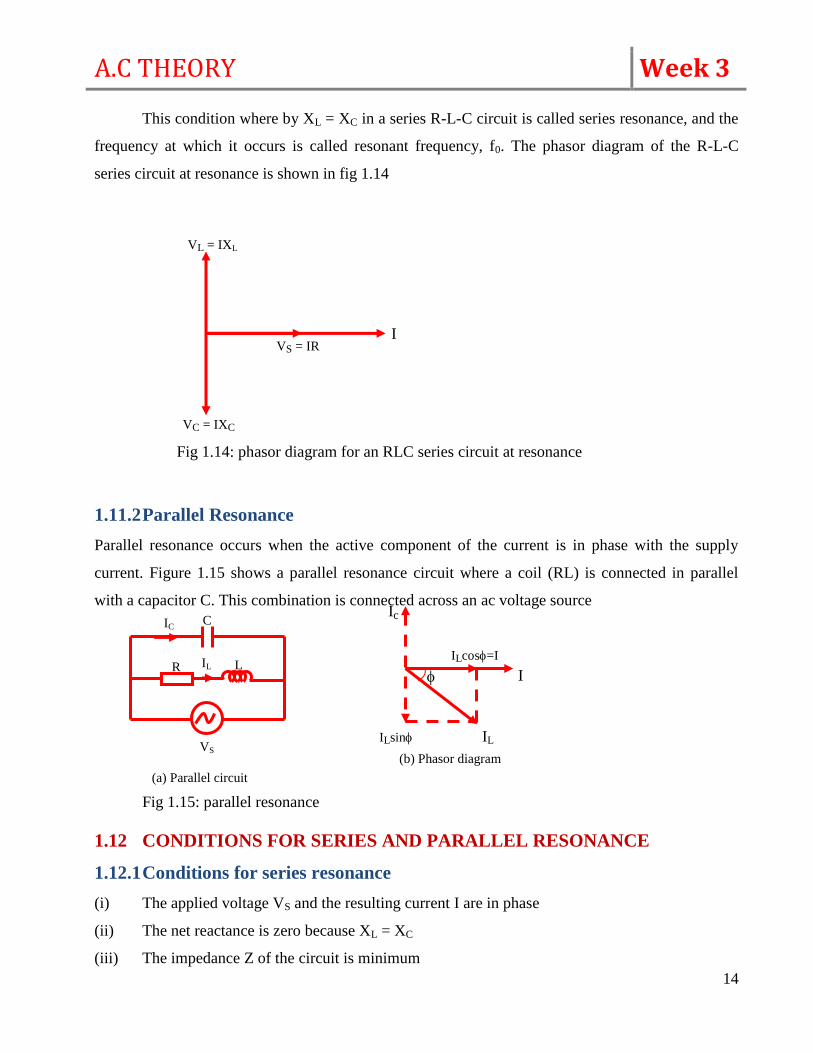
This condition where by XL = XC in a series R-L-C circuit is called series resonance, and the
frequency at which it occurs is called resonant frequency, f0. The phasor diagram of the R-L-C
series circuit at resonance is shown in fig 1.14
1.11.2 Parallel Resonance
Parallel resonance occurs when the active component of the current is in phase with the supply
current. Figure 1.15 shows a parallel resonance circuit where a coil (RL) is connected in parallel
with a capacitor C. This combination is connected across an ac voltage source
Fig 1.15: parallel resonance
1.12 CONDITIONS FOR SERIES AND PARALLEL RESONANCE
1.12.1 Conditions for series resonance
(i) The applied voltage VS and the resulting current I are in phase
(ii) The net reactance is zero because XL = XC
(iii) The impedance Z of the circuit is minimum
I
VL = IXL
VS = IR
VC = IXC
Fig 1.14: phasor diagram for an RLC series circuit at resonance
IC C
R IL
VS
L
(a) Parallel circuit
Ic
ILcos=I
I
IL ILsin
(b) Phasor diagram
A.C THEORY Week 3
15
(iv) The current in the circuit is maximum
(v) The resonant frequency is given by fr = 1 .
2π(LC)
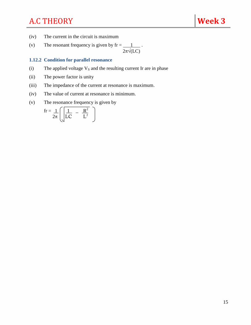
1.12.2 Condition for parallel resonance
(i) The applied voltage VS and the resulting current Ir are in phase
(ii) The power factor is unity
(iii) The impedance of the current at resonance is maximum.
(iv) The value of current at resonance is minimum.
(v) The resonance frequency is given by
fr = 1 1 _ R2
2π LC L2
A.C THEORY Week 4
1
At the end of this week, the students are expected to:
Prove the relevant formulae for Q-factor, dynamic impedance and bandwidth at resonance
frequency
Sketch current and impedance against frequency for series and parallel circuits
Calculate the Q-factor for a coil; loss factor for a capacitor
Explain with the aid of a diagram, bandwidth
Solve problems involving bandwidth and Q-factor
1.13 DERIVATIONS OF Q-FACTOR, DYNAMIC IMPEDENCE AND
BANDWIDTH AT RESONANCE FREQUENCY
1.13.1 Q-Factor of a Series Resonance
Q-factor = Potential drop across the inductance at resonance
Potential drop across the resistance at resonance
= IXL =XL/R = 2f0L (1.11)
IR R
Also, Q-factor = Potential drop across the capacitance at resonance
Potential drop across the resistance at resonance
=IXC = XC = 1
IR R 2f0CR (1.12)
1.13.2 Q-factor of a Parallel Resonance
Q-factor = Circulating current = ILSin (see fig 1.15b)
Supply current I
= tanL =XL = 2f0L (1.13)
R R
1.13.3 Dynamic Impedance of a Series Resonance
At series resonance, XL = XC and the impedance in the circuit is
Z=VS =ZD
I where ZD is known as dynamic impedance
ZD=VS = VS = VS = VS R2
= R
I VS / [R2 + (XL –XC)
2] VS / R
2 VS
ZD = R (1.14)
A.C THEORY Week 4
2
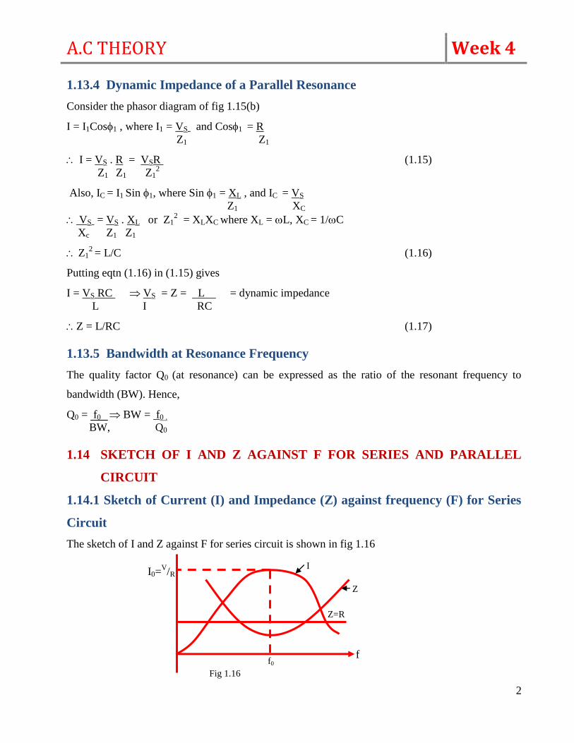
1.13.4 Dynamic Impedance of a Parallel Resonance
Consider the phasor diagram of fig 1.15(b)
I = I1Cos1 , where I1 = VS and Cos1 = R
Z1 Z1
I = VS . R = VSR (1.15)
Z1 Z1 Z12
Also, IC = I1 Sin 1, where Sin 1 = XL , and IC = VS
Z1 XC
VS = VS . XL or Z12 = XLXC where XL = L, XC = 1/C
Xc Z1 Z1
Z12
= L/C (1.16)
Putting eqtn (1.16) in (1.15) gives
I = VS RC VS = Z = L = dynamic impedance
L I RC
Z = L/RC (1.17)
1.13.5 Bandwidth at Resonance Frequency
The quality factor Q0 (at resonance) can be expressed as the ratio of the resonant frequency to
bandwidth (BW). Hence,
Q0 = f0 BW = f0 .
BW, Q0
1.14 SKETCH OF I AND Z AGAINST F FOR SERIES AND PARALLEL
CIRCUIT
1.14.1 Sketch of Current (I) and Impedance (Z) against frequency (F) for Series
Circuit
The sketch of I and Z against F for series circuit is shown in fig 1.16
I0=V/R
Z=R
Z
I
f0
Fig 1.16
f
A.C THEORY Week 4
3
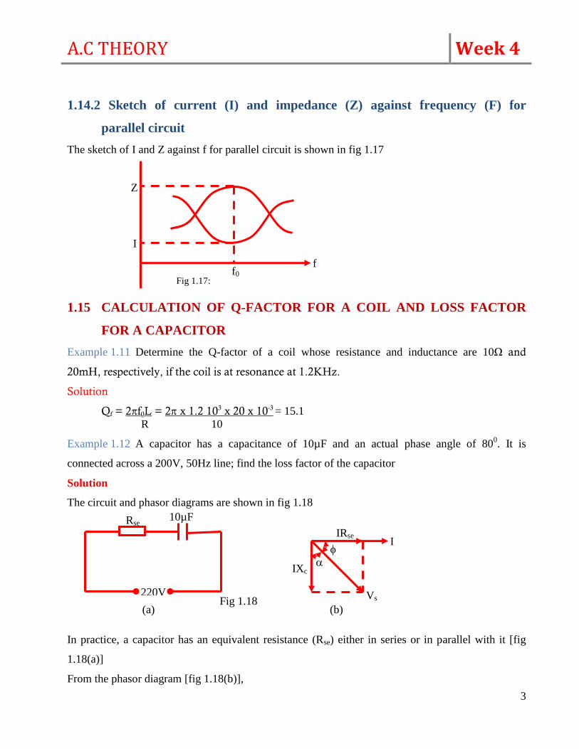
1.14.2 Sketch of current (I) and impedance (Z) against frequency (F) for
parallel circuit
The sketch of I and Z against f for parallel circuit is shown in fig 1.17
1.15 CALCULATION OF Q-FACTOR FOR A COIL AND LOSS FACTOR
FOR A CAPACITOR
Example 1.11 Determine the Q-factor of a coil whose resistance and inductance are 10Ω and
20mH, respectively, if the coil is at resonance at 1.2KHz.
Solution
Qf = 2πf0L = 2π x 1.2 103 x 20 x 10-3 = 15.1
R 10
Example 1.12 A capacitor has a capacitance of 10µF and an actual phase angle of 800. It is
connected across a 200V, 50Hz line; find the loss factor of the capacitor
Solution
The circuit and phasor diagrams are shown in fig 1.18
In practice, a capacitor has an equivalent resistance (Rse) either in series or in parallel with it [fig
1.18(a)]
From the phasor diagram [fig 1.18(b)],
220V
Rse 10µF
Fig 1.18
IRse
Vs
IXc
I
(b) (a)
Z
I
f f0
Fig 1.17:
A.C THEORY Week 4
4
= actual angle
= loss angle
and loss factor = tan
+ = 900, = 90
0 - = 90
0 - 80
0 = 10
0
and tan = tan100 = 0.1763
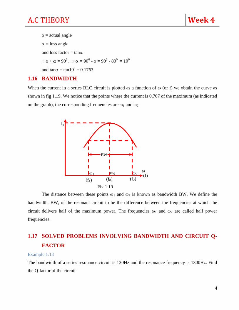
1.16 BANDWIDTH
When the current in a series RLC circuit is plotted as a function of (or f) we obtain the curve as
shown in fig 1.19. We notice that the points where the current is 0.707 of the maximum (as indicated
on the graph), the corresponding frequencies are 1 and 2.
The distance between these points 1 and 2 is known as bandwidth BW. We define the
bandwidth, BW, of the resonant circuit to be the difference between the frequencies at which the
circuit delivers half of the maximum power. The frequencies 1 and 2 are called half power
frequencies.
1.17 SOLVED PROBLEMS INVOLVING BANDWIDTH AND CIRCUIT Q-
FACTOR
Example 1.13
The bandwidth of a series resonance circuit is 130Hz and the resonance frequency is 1300Hz. Find
the Q-factor of the circuit
Io
(f1) (f0) (f2) (f)
1 0 2
BW
Fig 1.19
A.C THEORY Week 4
5
Solution
Qf = f0 = 1300 = 10
BW 130
Example 1.14 obtain the bandwidth in example 1.13 if the Q-factor is reduced by 50%
Solution
BW = f0 , where Q.f = 50 x 10 = 5
Q.f 100
BW = 1300 = 260Hz
5
Method of Analysis Week 5
1
At the end of this week, the students are expected to:
Explain the following terms used in electric networks:
Ideal and practical independent current and voltage sources
Branch
Node
Loop
Network
2.1 TERMS USED IN ELECTRIC NETWORK
The following terms are used in electric network:
(a) Ideal and Practical independent current and voltage sources
(b) Branch
(c) Node
(d) Loop
(e) Network
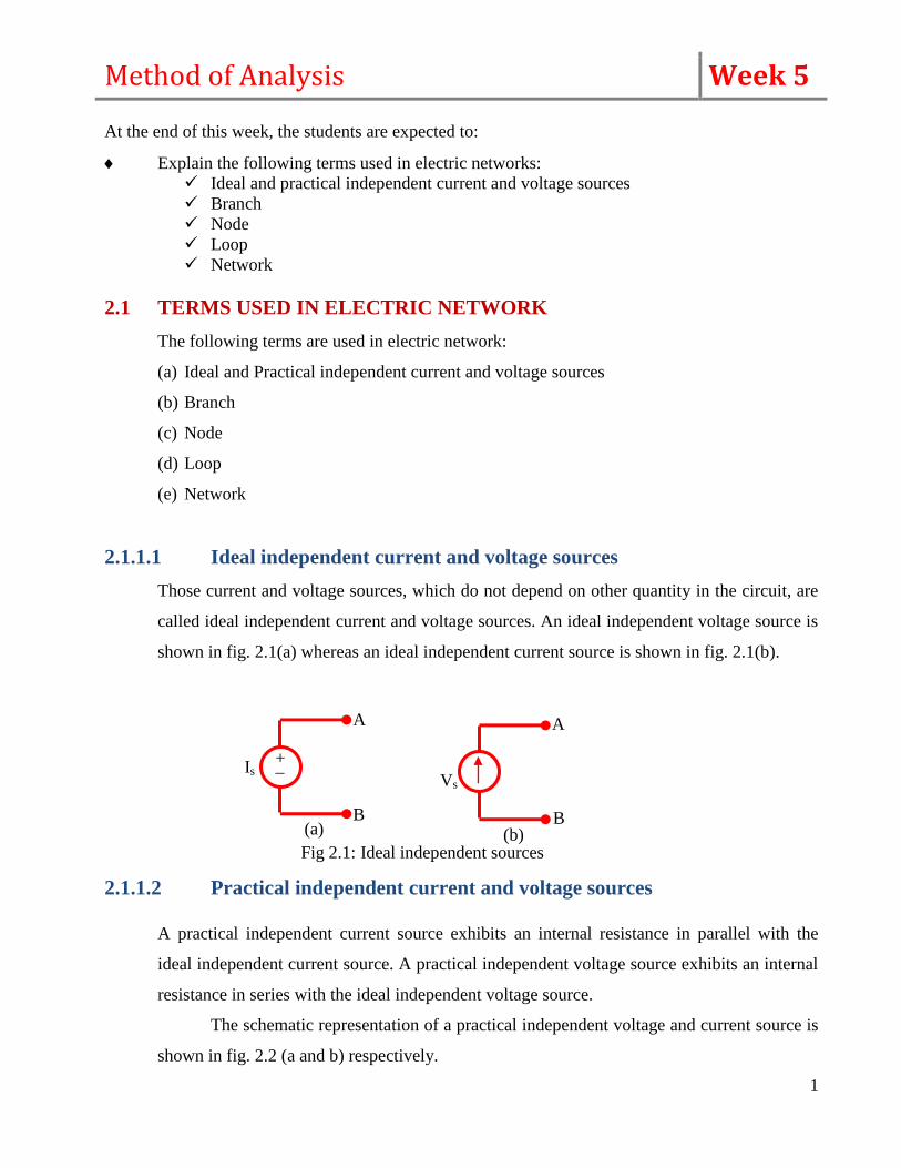
2.1.1.1 Ideal independent current and voltage sources
Those current and voltage sources, which do not depend on other quantity in the circuit, are
called ideal independent current and voltage sources. An ideal independent voltage source is
shown in fig. 2.1(a) whereas an ideal independent current source is shown in fig. 2.1(b).
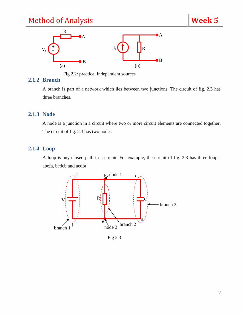
2.1.1.2 Practical independent current and voltage sources
A practical independent current source exhibits an internal resistance in parallel with the
ideal independent current source. A practical independent voltage source exhibits an internal
resistance in series with the ideal independent voltage source.
The schematic representation of a practical independent voltage and current source is
shown in fig. 2.2 (a and b) respectively.
+ _
A
B
Is
(a)
Vs
A
B (b)
Fig 2.1: Ideal independent sources
Method of Analysis Week 5
2
2.1.2 Branch
A branch is part of a network which lies between two junctions. The circuit of fig. 2.3 has
three branches.
2.1.3 Node
A node is a junction in a circuit where two or more circuit elements are connected together.
The circuit of fig. 2.3 has two nodes.
2.1.4 Loop
A loop is any closed path in a circuit. For example, the circuit of fig. 2.3 has three loops:
abefa, bedcb and acdfa
Is
A
B
(b)
R + _
A
B (a)
Vs
R
Fig 2.2: practical independent sources
a b c
d e f
V C R
branch 1 node 2 branch 2
branch 3
node 1
Fig 2.3
Method of Analysis Week 6
1
At the end of this week, the students are expected to:
Explain the basic principle of mesh circuit analysis
Solve problems on mesh circuit analysis
2.1.5 Network
A combination of various electric elements, connected in any manner whatsoever, is called a
network. This is shown in fig. 2.3
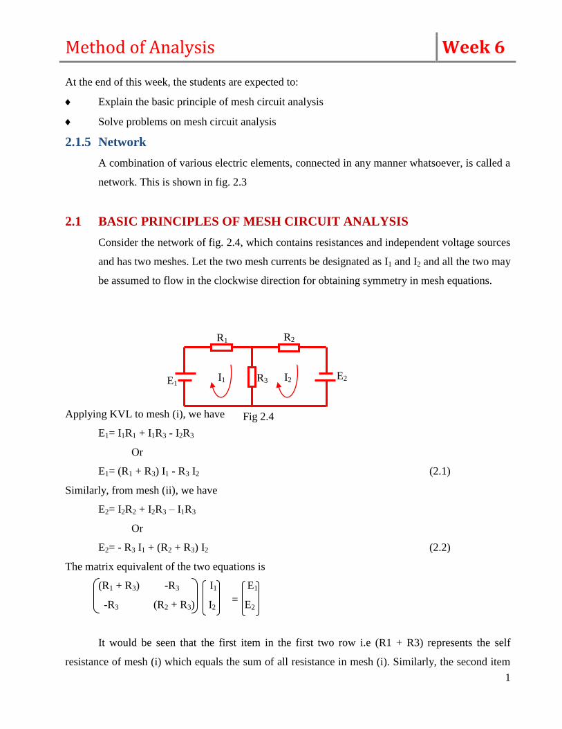
2.1 BASIC PRINCIPLES OF MESH CIRCUIT ANALYSIS
Consider the network of fig. 2.4, which contains resistances and independent voltage sources
and has two meshes. Let the two mesh currents be designated as I1 and I2 and all the two may
be assumed to flow in the clockwise direction for obtaining symmetry in mesh equations.
Applying KVL to mesh (i), we have
E1= I1R1 + I1R3 - I2R3
Or
E1= (R1 + R3) I1 - R3 I2 (2.1)
Similarly, from mesh (ii), we have
E2= I2R2 + I2R3 – I1R3
Or
E2= - R3 I1 + (R2 + R3) I2 (2.2)
The matrix equivalent of the two equations is
(R1 + R3) -R3 I1 E1
-R3 (R2 + R3) I2 E2
It would be seen that the first item in the first two row i.e (R1 + R3) represents the self
resistance of mesh (i) which equals the sum of all resistance in mesh (i). Similarly, the second item
E1 E2
R2 R1
R3 I1 I2
Fig 2.4
=
Method of Analysis Week 6
2
in the first row represents the mutual resistance between meshes (i) and (ii) i.e the sum of the
resistances common to mesh (i) and (ii).
The sign of the e.m.f’s, while going along the current, if we pass from negative to the
positive terminal of a battery, then, its e.m.f is taken positive. If it is the other way around, then
battery e.m.f is taken negative.
In the end, it may be pointed out that the directions of mesh currents can be selected
arbitrarily.
2.2 SOLVED PROBLEMS ON MESH CIRCUIT ANALYSIS
Example 2.1 Find V in figure 2.5 using mesh analysis
Solution
Using KVL for loops 1and 2, we get
20 = 4 I1 + 9(I1 – I2)
Or
20 = 13 I1 - 9I2 (2.3)
and 0 = 9(I2 – I1) + 32I2 +40I2
Or
0 = -9I1 +81I2 (2.4)
From equations (2.3) and (2.4), we get
Δ0 = = = 1053-81 = 972
Δ I1 = = 1620A
13 -9
-9 81
I1
I2
20
E1 0
13 -9
-9 81
20 -9
0 81
20V 40Ω
32Ω 4Ω
9Ω I1 I2
Fig 2.5
V
+
_
Method of Analysis Week 6
3
Δ I2 = = 18OA
I1 = ∆I1/∆0 = 1620/972 = 1.67A, I2 = ∆I2/∆0 = 180/972 = 0.185A
V = 40I2 = 40 x 0.19 7.4V
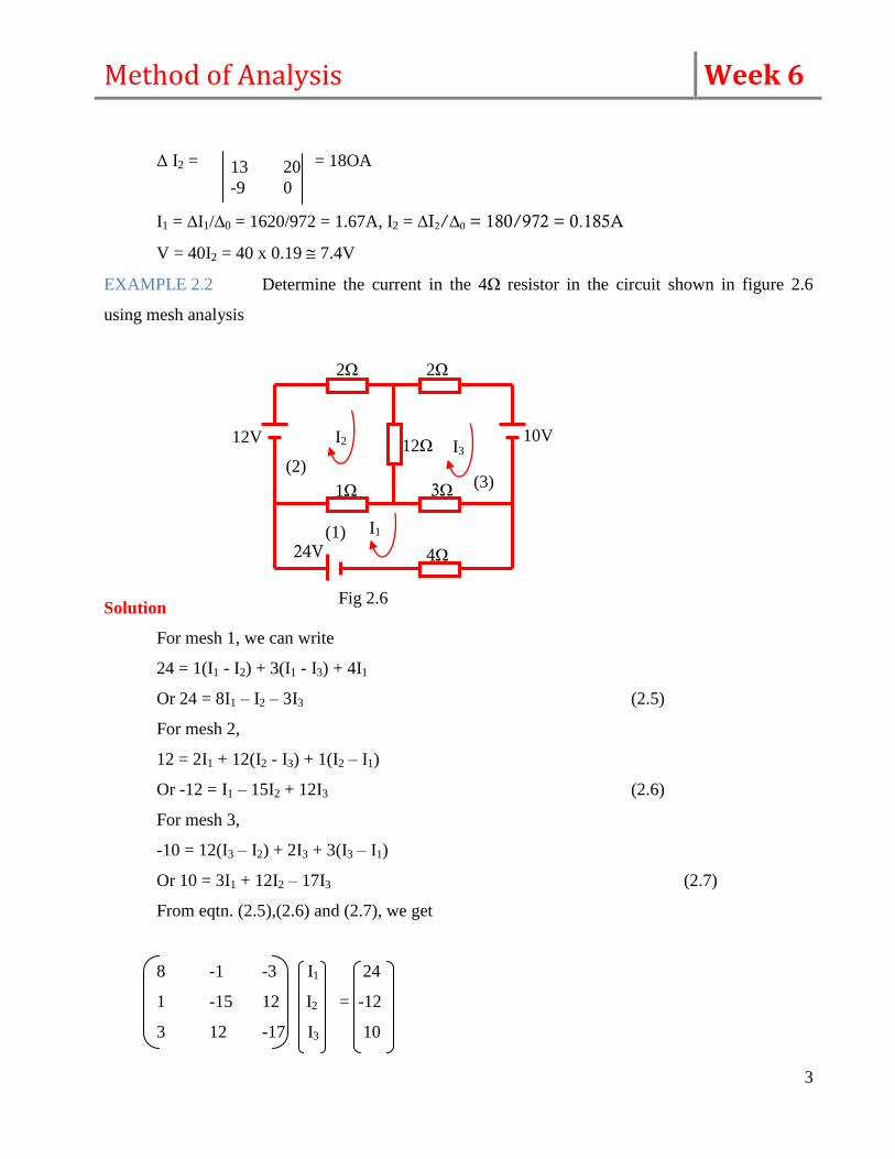
EXAMPLE 2.2 Determine the current in the 4Ω resistor in the circuit shown in figure 2.6
using mesh analysis
Solution
For mesh 1, we can write
24 = 1(I1 - I2) + 3(I1 - I3) + 4I1
Or 24 = 8I1 – I2 – 3I3 (2.5)
For mesh 2,
12 = 2I1 + 12(I2 - I3) + 1(I2 – I1)
Or -12 = I1 – 15I2 + 12I3 (2.6)
For mesh 3,
-10 = 12(I3 – I2) + 2I3 + 3(I3 – I1)
Or 10 = 3I1 + 12I2 – 17I3 (2.7)
From eqtn. (2.5),(2.6) and (2.7), we get
8 -1 -3 I1 24
1 -15 12 I2 = -12
3 12 -17 I3 10
13 20
-9 0
12V
2Ω 2Ω
10V 12Ω
1Ω 3Ω
4Ω 24V
I3 I2
I1
(2) (3)
(1)
Fig 2.6
Method of Analysis Week 6
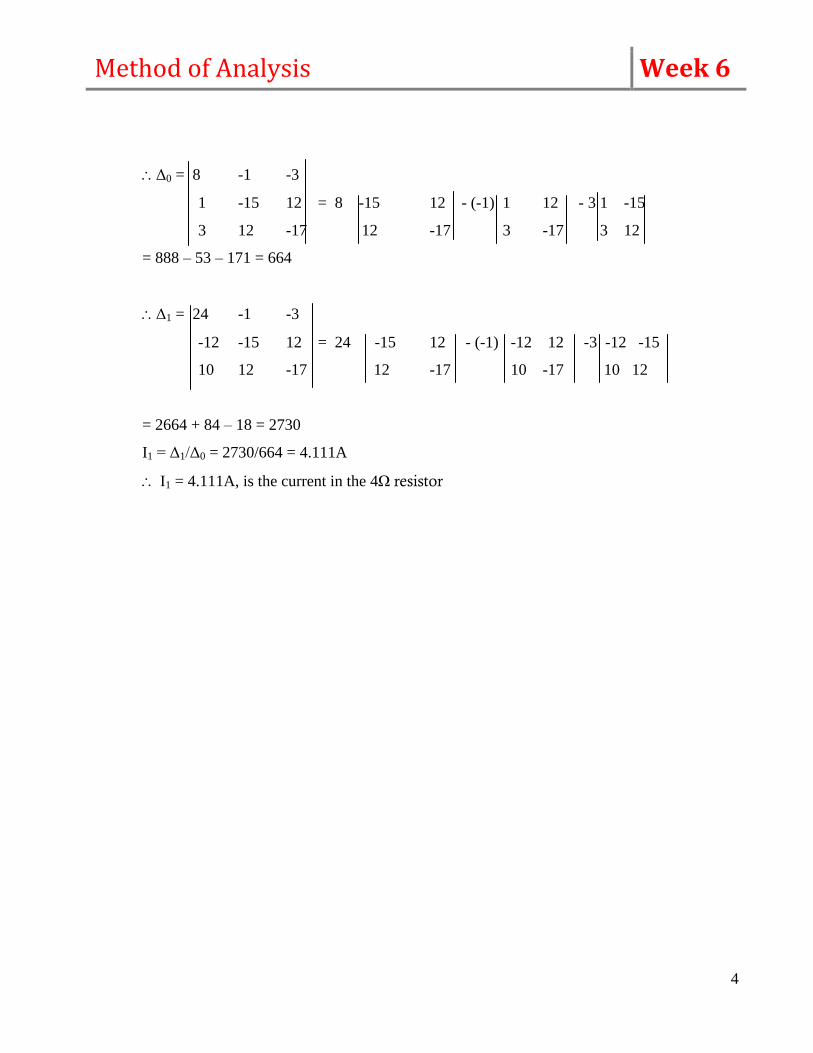
4
Δ0 = 8 -1 -3
1 -15 12 = 8 -15 12 - (-1) 1 12 - 3 1 -15
3 12 -17 12 -17 3 -17 3 12
= 888 – 53 – 171 = 664
Δ1 = 24 -1 -3
-12 -15 12 = 24 -15 12 - (-1) -12 12 -3 -12 -15
10 12 -17 12 -17 10 -17 10 12
= 2664 + 84 – 18 = 2730
I1 = Δ1/Δ0 = 2730/664 = 4.111A
I1 = 4.111A, is the current in the 4Ω resistor
Method of Analysis Week 7
1
At the end of this week, the students are expected to:
Explain the basic principle of nodal analysis
Solve problems on nodal analysis
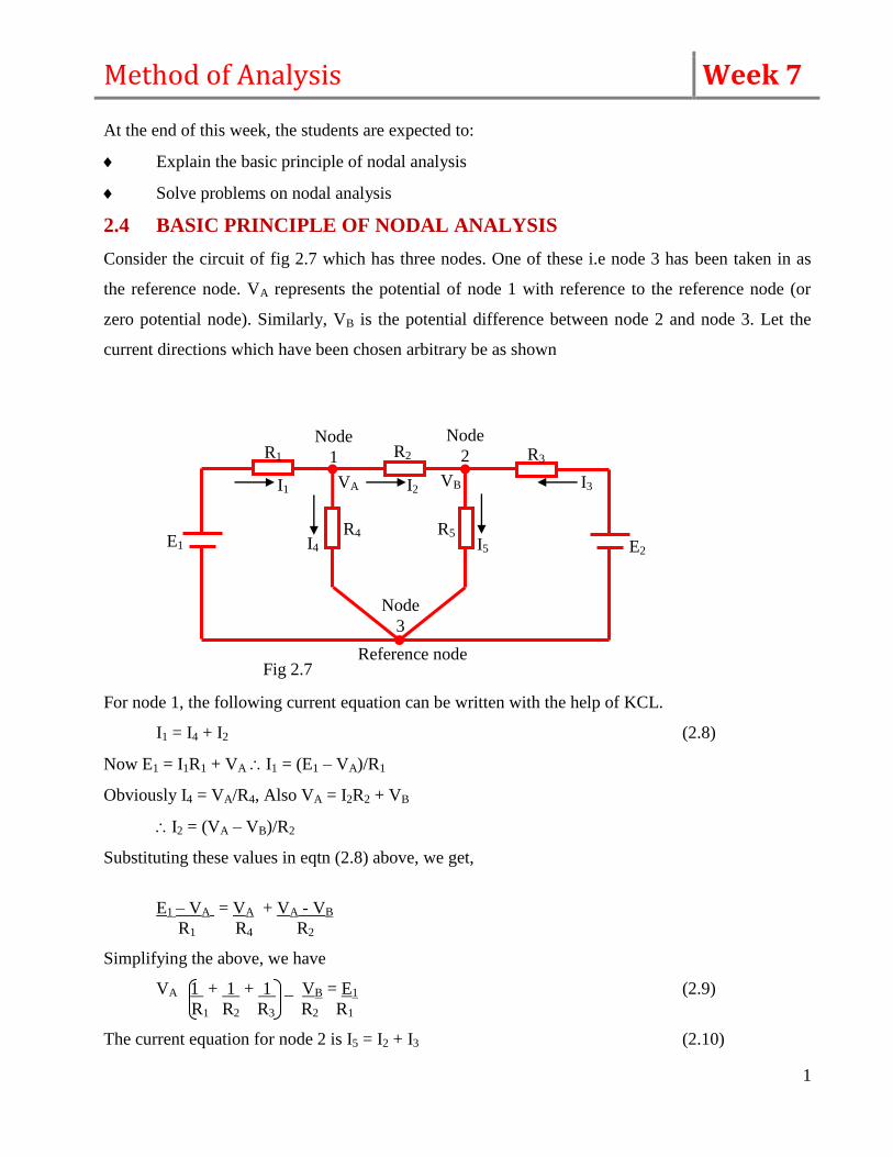
2.4 BASIC PRINCIPLE OF NODAL ANALYSIS
Consider the circuit of fig 2.7 which has three nodes. One of these i.e node 3 has been taken in as
the reference node. VA represents the potential of node 1 with reference to the reference node (or
zero potential node). Similarly, VB is the potential difference between node 2 and node 3. Let the
current directions which have been chosen arbitrary be as shown
For node 1, the following current equation can be written with the help of KCL.
I1 = I4 + I2 (2.8)
Now E1 = I1R1 + VA I1 = (E1 – VA)/R1
Obviously I4 = VA/R4, Also VA = I2R2 + VB
I2 = (VA – VB)/R2
Substituting these values in eqtn (2.8) above, we get,
E1 – VA = VA + VA - VB
R1 R4 R2
Simplifying the above, we have
VA 1 + 1 + 1 _ VB = E1 (2.9)
R1 R2 R3 R2 R1
The current equation for node 2 is I5 = I2 + I3 (2.10)
E1 E2
R3 R2 R1
R4 R5
VA VB I3 I2 I1
I4 I5
Node
3
Node
2 Node
1
Reference node Fig 2.7
Method of Analysis Week 7
2
Or VB = VA – VB + E2 - VB
R5 R2 R3
Or -VA + VB 1 + 1 + 1 = E2 (2.11)
R2 R2 R3 R5 R3
The node voltages in equation (2.9) and (2.11) are the unknowns and when determined by a suitable
method, result in the network solution. After finding different node voltages, various current can be
calculated by using ohm’s law.
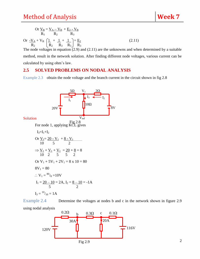
2.5 SOLVED PROBLEMS ON NODAL ANALYSIS
Example 2.3 obtain the node voltage and the branch current in the circuit shown in fig 2.8
Solution
For node 1, applying KCL gives
I3=I1+I2
Or V1= 20 - V1 + 8 - V1
10 5 2
V1 + V1 + V1 = 20 + 8 = 8
10 2 5 5 2
Or V1 + 5V1 + 2V1 = 8 x 10 = 80
8V1 = 80
V1 = 80
/8 =10V
I1 = 20 – 10 = 2A, I2 = 8 – 10 = -1A
5 2
I3 = 10
/10 = 1A
Example 2.4 Determine the voltages at nodes b and c in the network shown in figure 2.9
using nodal analysis
20V 8V
2Ω 5Ω
10Ω
V1
Vref
I2 I1
I3
Fig 2.8
120V 116V
30A
0.2Ω 0.3Ω 0.1Ω
20A
b c
Fig 2.9
Method of Analysis Week 7
3
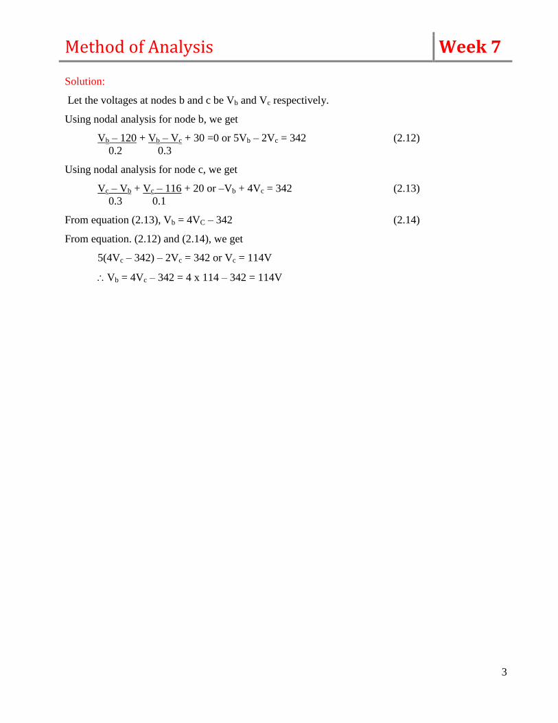
Solution:
Let the voltages at nodes b and c be Vb and Vc respectively.
Using nodal analysis for node b, we get
Vb – 120 + Vb – Vc + 30 =0 or 5Vb – 2Vc = 342 (2.12)
0.2 0.3
Using nodal analysis for node c, we get
Vc – Vb + Vc – 116 + 20 or –Vb + 4Vc = 342 (2.13)
0.3 0.1
From equation (2.13), Vb = 4VC – 342 (2.14)
From equation. (2.12) and (2.14), we get
5(4Vc – 342) – 2Vc = 342 or Vc = 114V
Vb = 4Vc – 342 = 4 x 114 – 342 = 114V
Network Transformation Week 8
1
At the end of this week, the students are expected to:
Reduce a complex network to its equivalent
Identify star and delta networks
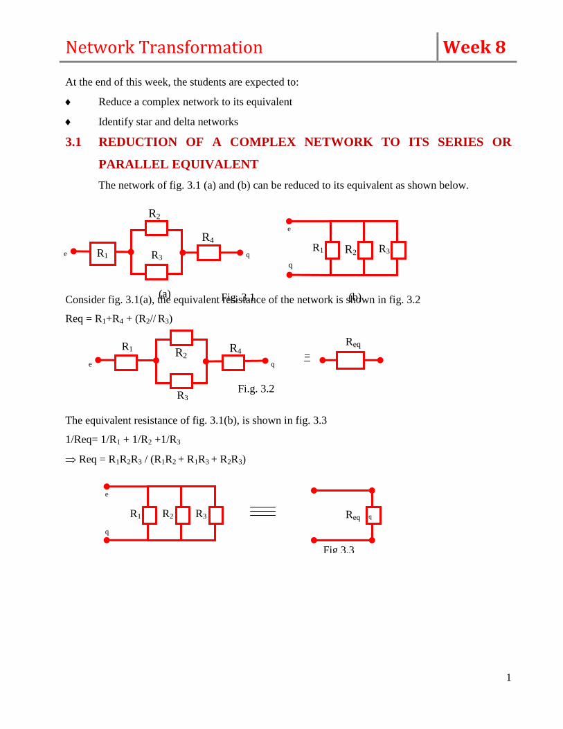
3.1 REDUCTION OF A COMPLEX NETWORK TO ITS SERIES OR
PARALLEL EQUIVALENT
The network of fig. 3.1 (a) and (b) can be reduced to its equivalent as shown below.
Consider fig. 3.1(a), the equivalent resistance of the network is shown in fig. 3.2
Req = R1+R4 + (R2// R3)
The equivalent resistance of fig. 3.1(b), is shown in fig. 3.3
1/Req= 1/R1 + 1/R2 +1/R3
Req = R1R2R3 / (R1R2 + R1R3 + R2R3)
e q =
Fi.g. 3.2
R1 R2
R3
R4 Req
e q
(a)
q
e
(b) Fig. 3.1
R1
R2
R3
R4 R1 R2 R3
Fig 3.3
q
q
e
R1 R2 R3 Req
Network Transformation Week 8
2
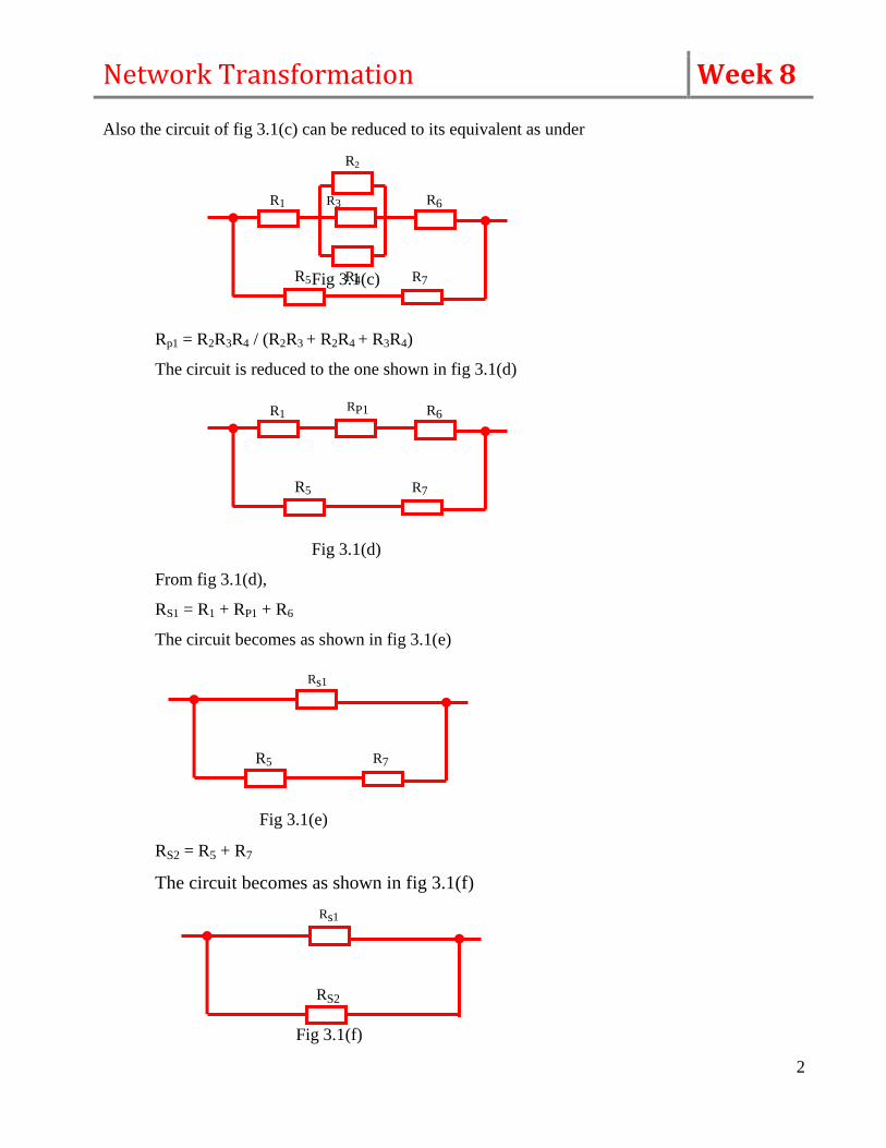
Also the circuit of fig 3.1(c) can be reduced to its equivalent as under
Fig 3.1(c)
Rp1 = R2R3R4 / (R2R3 + R2R4 + R3R4)
The circuit is reduced to the one shown in fig 3.1(d)
Fig 3.1(d)
From fig 3.1(d),
RS1 = R1 + RP1 + R6
The circuit becomes as shown in fig 3.1(e)
Fig 3.1(e)
RS2 = R5 + R7
The circuit becomes as shown in fig 3.1(f)
R5
R1
R2
R3
R4
R6
R7
R5
R1 RP1
R6
R7
Rs1
R5 R7
RS2
Rs1
Fig 3.1(f)
Network Transformation Week 8
3
Req = RS2 + RS1
The circuit is finally reduced as shown in fig 3.1(g)
Fig 3.1(g)
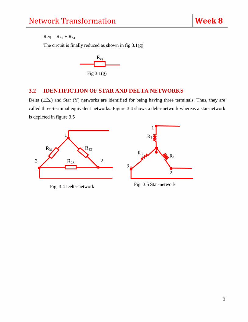
3.2 IDENTIFICTION OF STAR AND DELTA NETWORKS
Delta ( ) and Star (Y) networks are identified for being having three terminals. Thus, they are
called three-terminal equivalent networks. Figure 3.4 shows a delta-network whereas a star-network
is depicted in figure 3.5
Fig. 3.4 Delta-network
R31
R23
R12
1
2 3
R2 R3
R1
Fig. 3.5 Star-network
1
2
3
Req
Network Transformation Week 9
1
At the end of this week, the students are expected to:
Derive the formula for the transformation of a delta to a star network and vice versa
Solve problems on Delta to star transformation
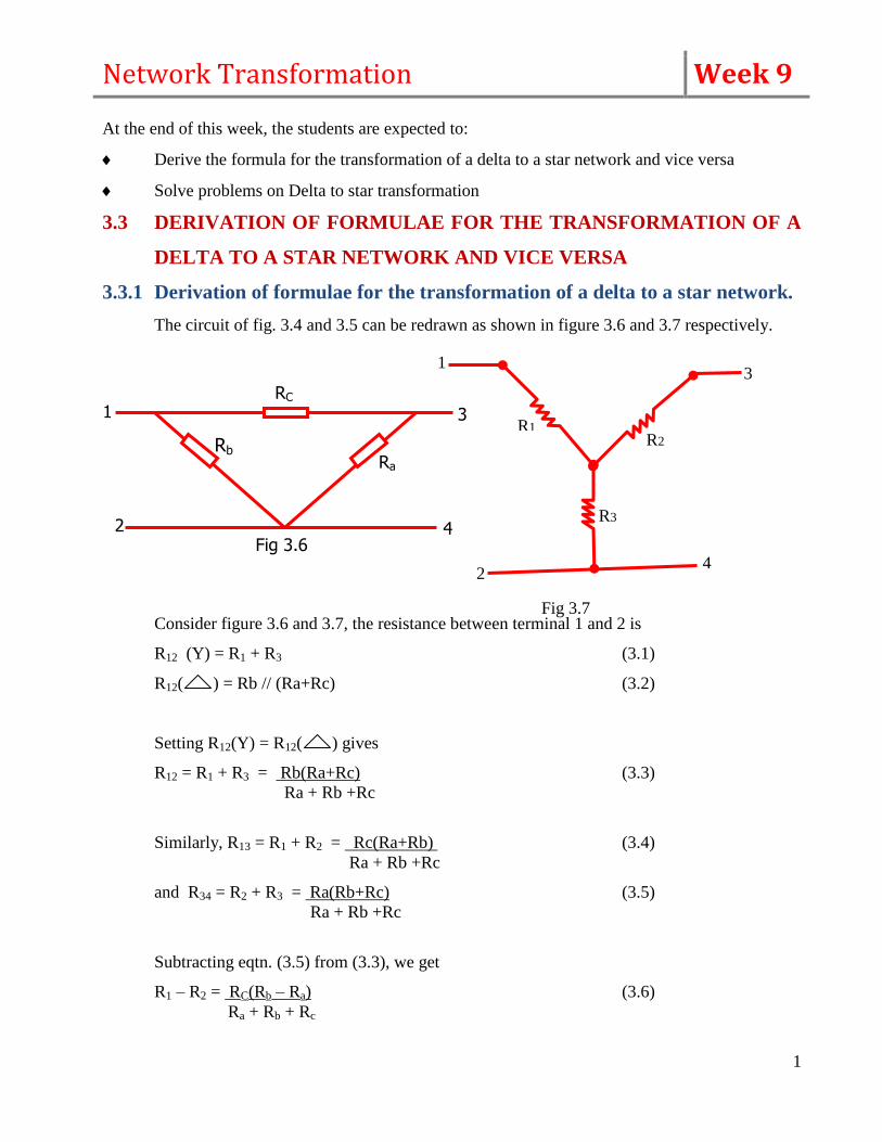
3.3 DERIVATION OF FORMULAE FOR THE TRANSFORMATION OF A
DELTA TO A STAR NETWORK AND VICE VERSA
3.3.1 Derivation of formulae for the transformation of a delta to a star network.
The circuit of fig. 3.4 and 3.5 can be redrawn as shown in figure 3.6 and 3.7 respectively.
Consider figure 3.6 and 3.7, the resistance between terminal 1 and 2 is
R12 (Y) = R1 + R3 (3.1)
R12( ) = Rb // (Ra+Rc) (3.2)
Setting R12(Y) = R12( ) gives
R12 = R1 + R3 = Rb(Ra+Rc) (3.3)
Ra + Rb +Rc
Similarly, R13 = R1 + R2 = Rc(Ra+Rb) (3.4)
Ra + Rb +Rc
and R34 = R2 + R3 = Ra(Rb+Rc) (3.5)
Ra + Rb +Rc
Subtracting eqtn. (3.5) from (3.3), we get
R1 – R2 = RC(Rb – Ra) (3.6)
Ra + Rb + Rc
Fig 3.6
R2
R3
R1
1
2
3
4
Fig 3.7
Fig 3.6
Rb
Ra
aa
RC
3
4
2
1
Network Transformation Week 9
2
Adding eqtn. (3.4) and (3.6) gives
R1 = RbRc (3.7)
Ra + Rb + Rc
Subtracting eqtn. (3.6) from (3.4) gives
R2 = RcRa (3.8)
Ra+Rb+Rc
Subtracting eqtn. (3.7) from eqtn. (3.3) gives
R3 = RaRb (3.9)
Ra+Rb+Rc
Eqtn. (3.7) to (3.9) is the required conversion formulae
3.3.2 Derivation of formulae for the transformation of a star to a delta network
Multiplying equation (3.7) and (3.8), (3.8) and (3.9), (3.7) and (3.9) and adding them
together gives,
R1R2+ R2R3+ R1R3 = RaRbRc (RaRbRc)
(Ra+Rb+Rc)2
= RaRbRc (3.10)
Ra+Rb+Rc
Dividing eqtn. (3.10) by each of eqtn. (3.7) to (3.9) gives
Ra = R1R2+ R2R3+ R1R3 (3.11)
R1
Rb = R1R2+ R2R3+ R1R3 (3.12)
R2
Rc = R1R2+ R2R3+ R1R3 (3.13)
R3
Equation (3.11) to (3.13) is the required conversion formulae
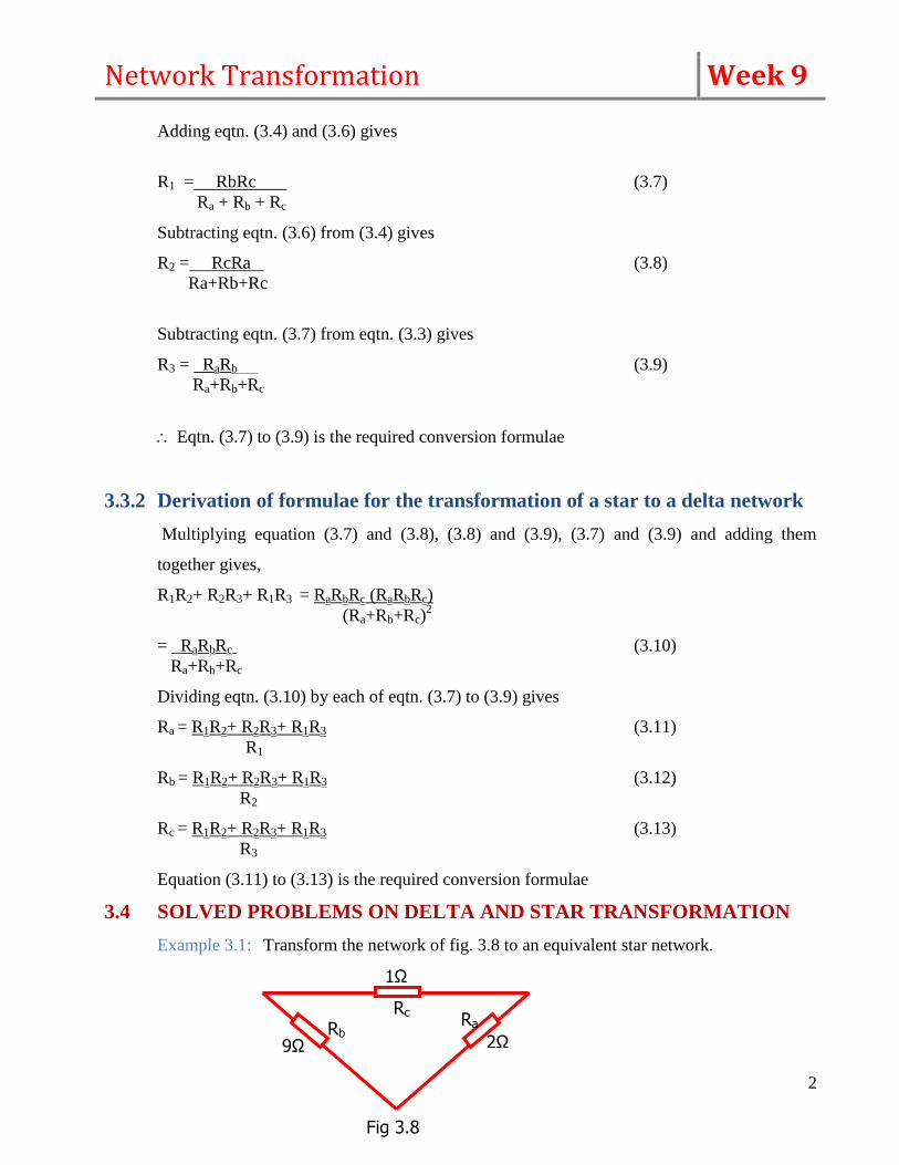
3.4 SOLVED PROBLEMS ON DELTA AND STAR TRANSFORMATION
Example 3.1: Transform the network of fig. 3.8 to an equivalent star network.
Fig 3.8
Rc Rb
Ra
aa
9Ω
2Ω
1Ω
Network Transformation Week 9
3
Solution
R1 = RaRb = 1 X 9 = 0.75Ω
Ra + Rb + Rc 2+9+1
R2 = RaRc = 2X1 = 2 = 1/6Ω
Ra + Rb + Rc 2+9+1 12
R3 = RbRc = 9X2 = 1.5Ω
Ra + Rb + Rc 9+2+1
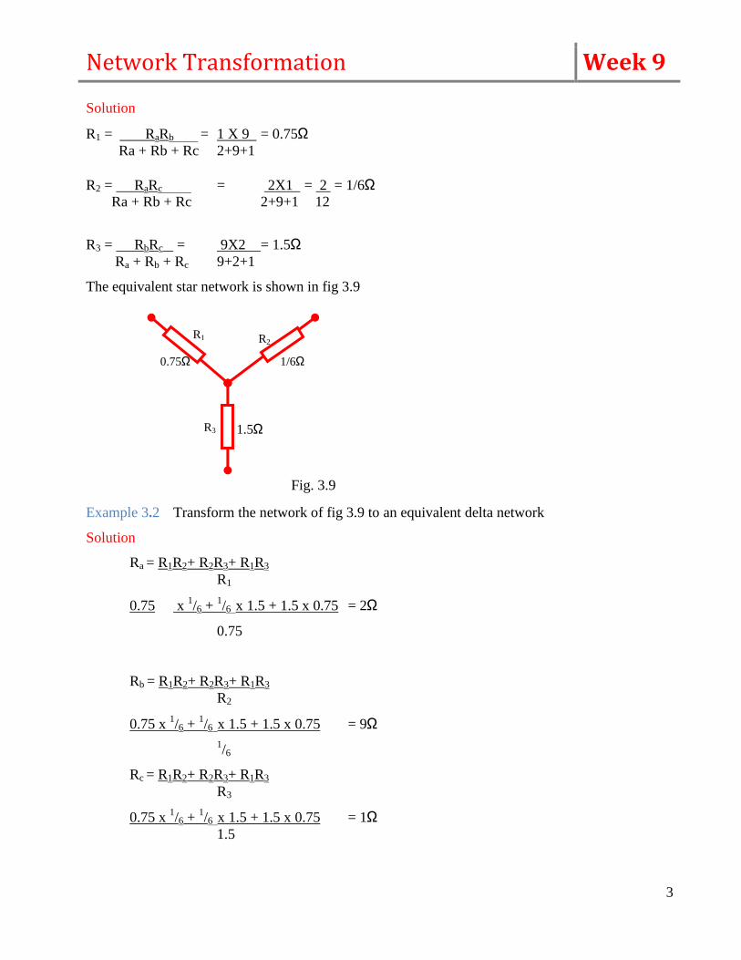
The equivalent star network is shown in fig 3.9
Example 3.2 Transform the network of fig 3.9 to an equivalent delta network
Solution
Ra = R1R2+ R2R3+ R1R3
R1
0.75 x 1/6 +
1/6 x 1.5 + 1.5 x 0.75 = 2Ω
0.75
Rb = R1R2+ R2R3+ R1R3
R2
0.75 x 1/6 +
1/6 x 1.5 + 1.5 x 0.75 = 9Ω
1/6
Rc = R1R2+ R2R3+ R1R3
R3
0.75 x 1/6 +
1/6 x 1.5 + 1.5 x 0.75 = 1Ω
1.5
R1 R2
R3 1.5Ω
1/6Ω 0.75Ω
Fig. 3.9
Network Transformation Week 10
1
At the end of this week, the students are expected to:
Explain the meaning of duality principle
Establish duality between resistance, conductance, inductance, capacitance, voltage and current.
3.5 DUALITY PRINCIPLE
Consider for example, the relationship between series and parallel circuits. In a series circuit,
individual voltages are added and in a parallel circuit, individual currents are added. It is
seen that while comparing series and parallel circuits,voltage takes the place of current and
current takes the place of voltage. Such a pattern is known as duality principle.
3.6 DUALITY BETWEEN RESISTANCE, CONDUCTANCE,
INDUCTANCE, CAPACITANCE, VOLTAGE AND CURRENT.
The duality between resistance, conductance, inductance, capacitance, voltage and current is
tabulated as shown in table 3.1
Table 3.1
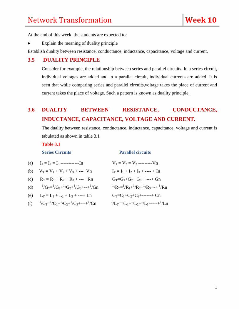
Series Circuits Parallel circuits
(a) I1 = I2 = I3 ------------In V1 = V2 = V3 ---------Vn
(b) VT = V1 + V2 + V3 + ---+Vn IT = I1 + I2 + I3 + ---- + In
(c) RT = R1 + R2 + R3 + ---+ Rn GT=G1+G2+ G3 + ---+ Gn
(d) 1/GT=
1/G1+
1/G2+
1/G3+--+
1/Gn
1/RT=
1/R1+
1/R2+
1/R3+-+
1/Rn
(e) LT = L1 + L2 + L3 + ---+ Ln CT=C1+C2+C3+------+ Cn
(f) 1/CT=
1/C1+
1/C2+
1/C3+---+
1/Cn
1/LT=
1/L1+
1/L2+
1/L3+----+
1/Ln
Network Transformation Week 11
1
At the end of this week, the students are expected to:
Find the duality of a network
Solve network problems using duality principle
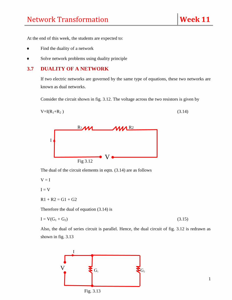
3.7 DUALITY OF A NETWORK
If two electric networks are governed by the same type of equations, these two networks are
known as dual networks.
Consider the circuit shown in fig. 3.12. The voltage across the two resistors is given by
V=I(R1+R2 ) (3.14)
The dual of the circuit elements in eqtn. (3.14) are as follows
V = I
I = V
R1 + R2 = G1 + G2
Therefore the dual of equation (3.14) is
I = V(G1 + G2) (3.15)
Also, the dual of series circuit is parallel. Hence, the dual circuit of fig. 3.12 is redrawn as
shown in fig. 3.13
G1 G2
Fig. 3.13
V
I
R1 R2
V
I
Fig 3.12
Network Transformation Week 11
2
3.8 SOLVED NETWORK PROBLEMS USING DUALITY PRINCIPLE
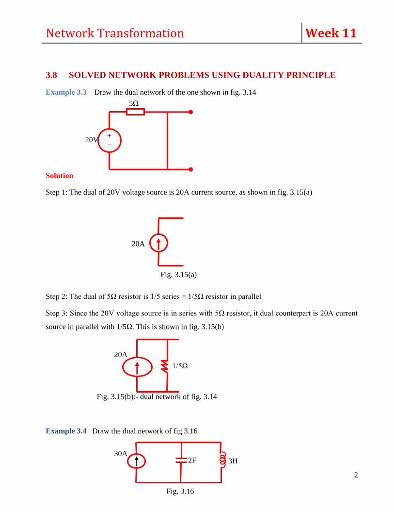
Example 3.3 Draw the dual network of the one shown in fig. 3.14
Solution
Step 1: The dual of 20V voltage source is 20A current source, as shown in fig. 3.15(a)
Step 2: The dual of 5Ω resistor is 1/5 series = 1/5Ω resistor in parallel
Step 3: Since the 20V voltage source is in series with 5Ω resistor, it dual counterpart is 20A current
source in parallel with 1/5Ω. This is shown in fig. 3.15(b)
Example 3.4 Draw the dual network of fig 3.16
Fig. 3.15(a)
20A
20A
1/5Ω
Fig. 3.15(b):- dual network of fig. 3.14
+ _
5
20V
Fig. 3.16
30A 3H 2F
Network Transformation Week 11
3
Solution
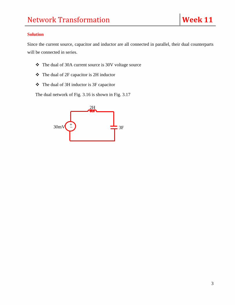
Since the current source, capacitor and inductor are all connected in parallel, their dual counterparts
will be connected in series.
The dual of 30A current source is 30V voltage source
The dual of 2F capacitor is 2H inductor
The dual of 3H inductor is 3F capacitor
The dual network of Fig. 3.16 is shown in Fig. 3.17
+ _
2H
3F 30mV
Network Theorems Week 12
1
At the end of this week, the students are expected to:
State Thevenin’s theorem
Explain the basic principle of Thevenin’s theorem
Solve problems on simple network using Thevenin’s theorem
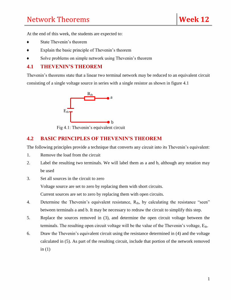
4.1 THEVENIN’S THEOREM
Thevenin’s theorems state that a linear two terminal network may be reduced to an equivalent circuit
consisting of a single voltage source in series with a single resistor as shown in figure 4.1
4.2 BASIC PRINCIPLES OF THEVENIN’S THEOREM
The following principles provide a technique that converts any circuit into its Thevenin’s equivalent:
1. Remove the load from the circuit
2. Label the resulting two terminals. We will label them as a and b, although any notation may
be used
3. Set all sources in the circuit to zero
Voltage source are set to zero by replacing them with short circuits.
Current sources are set to zero by replacing them with open circuits.
4. Determine the Thevenin’s equivalent resistance, Rth, by calculating the resistance “seen”
between terminals a and b. It may be necessary to redraw the circuit to simplify this step.
5. Replace the sources removed in (3), and determine the open circuit voltage between the
terminals. The resulting open circuit voltage will be the value of the Thevenin’s voltage, Eth.
6. Draw the Thevenin’s equivalent circuit using the resistance determined in (4) and the voltage
calculated in (5). As part of the resulting circuit, include that portion of the network removed
in (1)
Rth
Eth
a
b
Fig 4.1: Thevenin’s equivalent circuit
Network Theorems Week 12
2
4.3 SOLVED PROBLEMS ON SIMPLE NETWORK USING THEVENIN’S
THEOREM
Example 4.1 Obtain the Thevenin’s equivalent circuit for the active network in fig 4.2(a).
Solution
With terminals ab open, the current through the 3 and 6 resistor is
I = 18 = 2A
3 + 6
The Thevenin’s voltage VTh, is the voltage across terminal a-b.
Hence, Vab = Vth = I X 6 = 2 X 6 = 12V
The Thevenin’s resistance can be obtained by shorting out the 18V sources [fig 4.2(b)] and finding
the equivalent resistance of this network at terminals ab:
RTh = 3 + 3 x 6 = 5
3 + 6
The Thevenin’s equivalent circuit is shown in fig 4.3
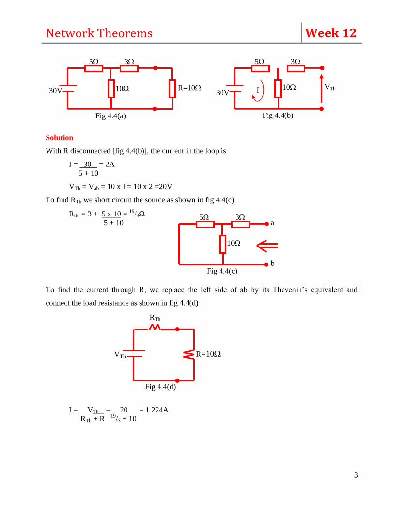
Example 4.2 Applying Thevenin’s theorem to find the current through the resistance R as shown
in figure 4.4(a)
a
3 6
3
b (b)
Fig 4.2
18V
3
6
3
a
b (a)
I
Rth
Eth
a
b
Fig 4.3: Thevenin’s equivalent circuit
Network Theorems Week 12
3
Solution
With R disconnected [fig 4.4(b)], the current in the loop is
I = 30 = 2A
5 + 10
VTh = Vab = 10 x I = 10 x 2 =20V
To find RTh we short circuit the source as shown in fig 4.4(c)
Rth = 3 + 5 x 10 = 19
/3
5 + 10
To find the current through R, we replace the left side of ab by its Thevenin’s equivalent and
connect the load resistance as shown in fig 4.4(d)
I = VTh = 20 = 1.224A
RTh + R 19
/3 + 10
10 R=10
5 3
30V
Fig 4.4(a)
10 VTh
5 3
30V
Fig 4.4(b)
I
10
5 3
Fig 4.4(c)
a
b
RTh
R=10 VTh
Fig 4.4(d)
Network Theorems Week 13
1
At the end of this week, the students are expected to:
State Norton’s theorem
Explain the basic principle of Norton’s theorem
Compare Norton’s theorem with Thevenin’s theorem
Solve simple problems on Norton’s theorem
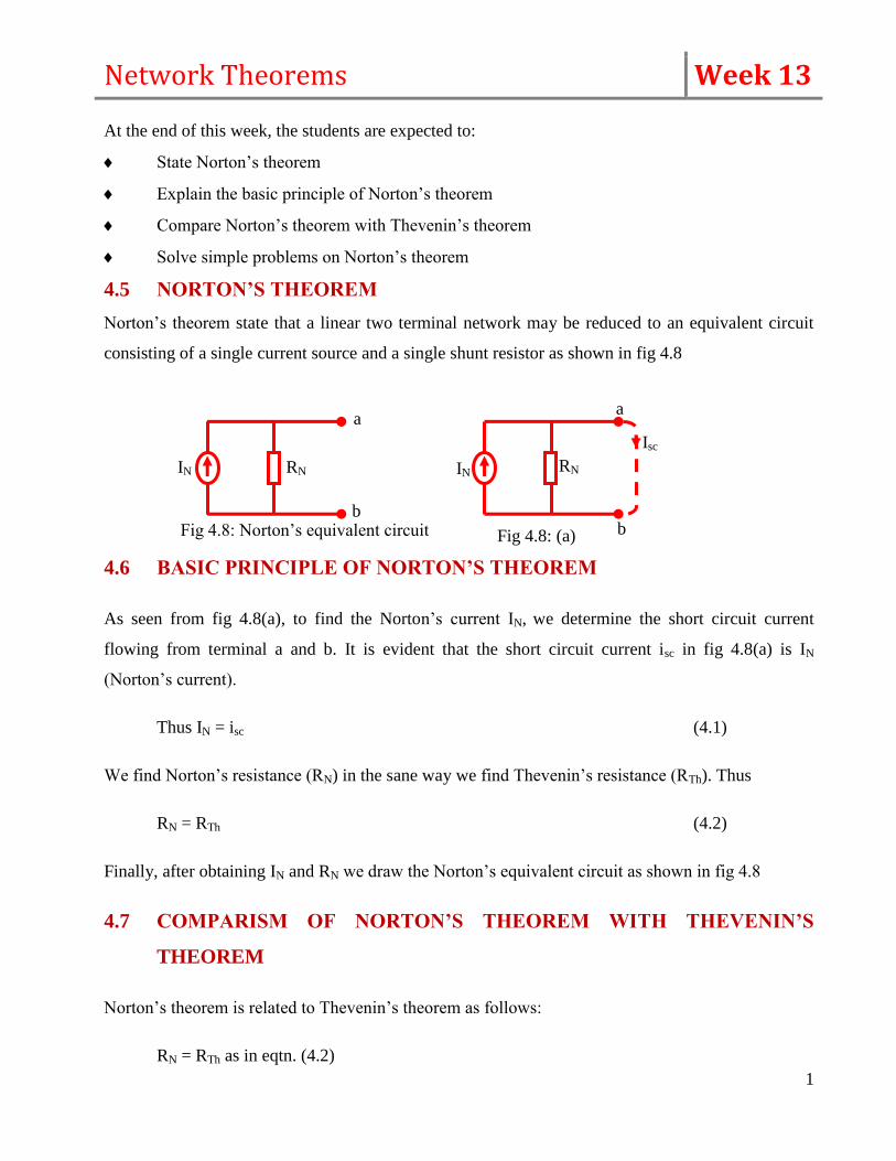
4.5 NORTON’S THEOREM
Norton’s theorem state that a linear two terminal network may be reduced to an equivalent circuit
consisting of a single current source and a single shunt resistor as shown in fig 4.8
4.6 BASIC PRINCIPLE OF NORTON’S THEOREM
As seen from fig 4.8(a), to find the Norton’s current IN, we determine the short circuit current
flowing from terminal a and b. It is evident that the short circuit current isc in fig 4.8(a) is IN
(Norton’s current).
Thus IN = isc (4.1)
We find Norton’s resistance (RN) in the sane way we find Thevenin’s resistance (RTh). Thus
RN = RTh (4.2)
Finally, after obtaining IN and RN we draw the Norton’s equivalent circuit as shown in fig 4.8
4.7 COMPARISM OF NORTON’S THEOREM WITH THEVENIN’S
THEOREM
Norton’s theorem is related to Thevenin’s theorem as follows:
RN = RTh as in eqtn. (4.2)
Fig 4.8: Norton’s equivalent circuit
IN RN
a
b
a
b
RN IN
Fig 4.8: (a)
Isc
Network Theorems Week 13
2
IN = VTh/RTh (4.3)
Also, IN = VTh/RN (4.4)
4.8 SOLVED PROBLEMS USING NORTON’S THEOREM
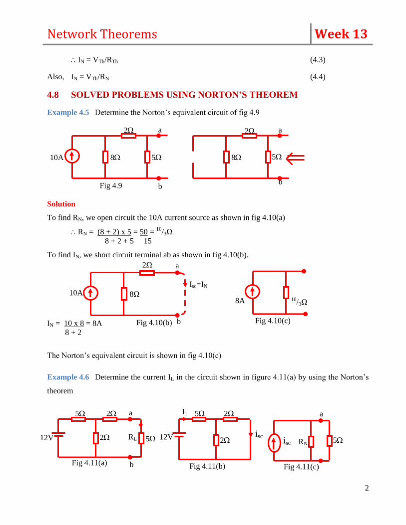
Example 4.5 Determine the Norton’s equivalent circuit of fig 4.9
Solution
To find RN, we open circuit the 10A current source as shown in fig 4.10(a)
RN = (8 + 2) x 5 = 50 = 10
/3Ω
8 + 2 + 5 15
To find IN, we short circuit terminal ab as shown in fig 4.10(b).
IN = 10 x 8 = 8A
8 + 2
The Norton’s equivalent circuit is shown in fig 4.10(c)
Example 4.6 Determine the current IL in the circuit shown in figure 4.11(a) by using the Norton’s
theorem
10A 8
2
5
b
a
Fig 4.9
a
b
8 5
2
Fig 4.10(b)
10A
2Ω
8Ω
Isc=IN
a
b Fig 4.10(c)
10/3Ω 8A
Fig 4.11(b)
12V 2
5 2
isc
I1
12V
2 5 a
2 5 RL
b
a
Fig 4.11(a)
5 isc RN
a
Fig 4.11(c)
Network Theorems Week 13
3
Solution
With RL disconnected and replaced by short circuit [fig 4.11(b)],
I1 = 12 .
5 + 2 x 2 = 2A
2 + 2
isc = 2 x 2 = 1A = IN
2 + 2
To find RN, the voltage is replaced by a short circuit,
RN = 2 + 5 x 2 = 24
5 + 2 7
The Norton’s equivalent circuit with RL connected across terminal ab is shown in fig 4.11(c).
IL = isc RN = 1 x 24
/7 = 0.407A
RN + 5 24
/7 + 5
Network Theorems Week 14
1
At the end of this week, the students are expected to:
State Millman’s theorem
Explain the basic principle of Millman’s theorem
Solve network problems using Millman’s theorem
4.9 MILLIMAN’S THEOREM
This states that any number of parallel voltage sources E1, E2,……,En having internal resistance R1,
R2,…….,Rn respectively can be replaced by a single equivalent source E in series with an equivalent
series resistance R.
4.10 BASIC PRINCIPLE OF MILLIMAN’S THEOREM
In circuits of the type shown in figure 4.12, the voltage sources may be replaced with a single
equivalent source as shown in figure 4.13
The values of I1, I2 ……In would be determined using ohm’s law:
I1 = E1/R1, I2 = E2/R2, …… In = En/Rn
Hence the equivalent current in the circuit is given by
Ieq = I1 + I2 + ….. + In (4.5)
The equivalent resistance Req is obtain by short circuiting the voltage sources. The resistance seen
via terminal ab when RL is removed is given by
Req = R1//R2 // ….//Rn (4.6)
Which may be determined as
Req = 1 (4.7)
1/R1 +
1/R2 + …. +
1/Rn
The general expression for the equivalent voltage is
Eeq = IeqReq = E1 + E2 + E3 + ….. + En
R1 R2 R3 Rn . (4.8)
1/R1 +
1/R2 +
1/R3 + …..+
1/Rn
I1 I2
E1 E2 En
b
a
R1 R2 Rn
RL In
Fig 4.12
RL
Req
Eeq
Fig 4.13
a
b
Network Theorems Week 14
2
4.11 SOLVED NETWORK PROBLEMS USING MILLIMAN’S THEOREM
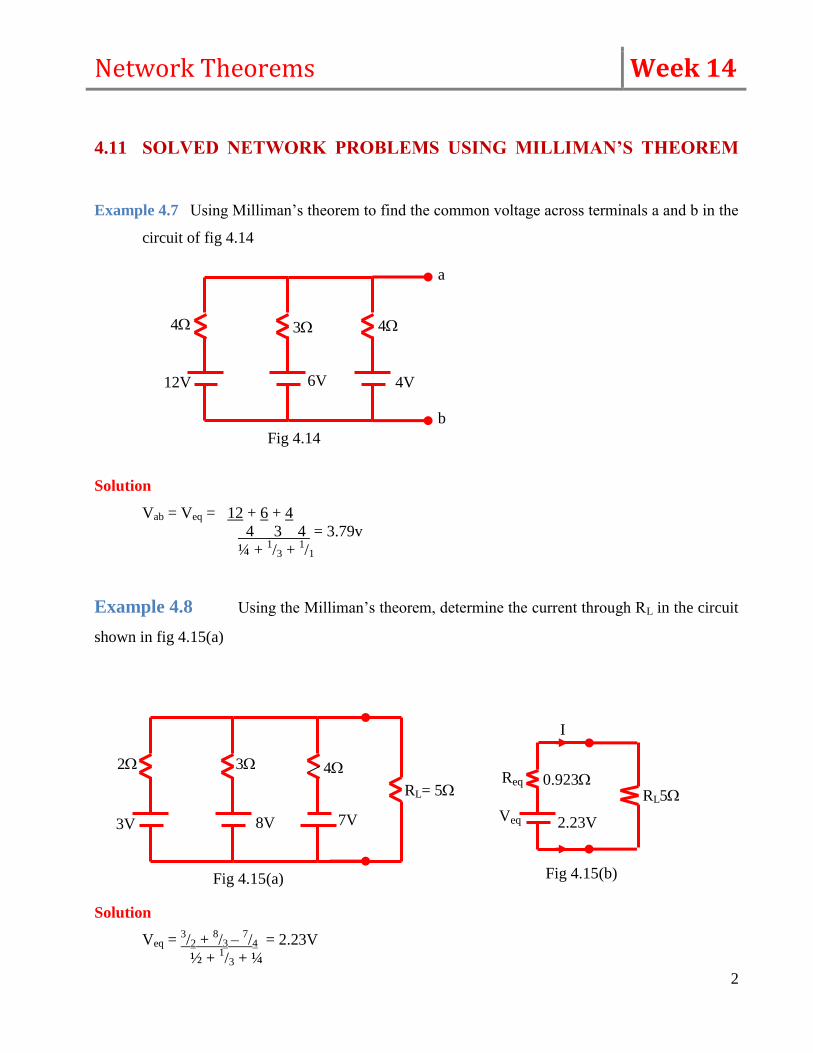
Example 4.7 Using Milliman’s theorem to find the common voltage across terminals a and b in the
circuit of fig 4.14
Solution
Vab = Veq = 12 + 6 + 4
4 3 4 = 3.79v
¼ + 1/3 +
1/1
Example 4.8 Using the Milliman’s theorem, determine the current through RL in the circuit
shown in fig 4.15(a)
Solution
Veq = 3/2 +
8/3
–
7/4 = 2.23V
½ + 1/3 + ¼
12V 6V 4V
b
a
4 3 4
Fig 4.14
3V 8V 7V
4
RL= 5
Fig 4.15(a)
3 2
RL5 Req
Veq
Fig 4.15(b)
I
0.923
2.23V
Network Theorems Week 14
3
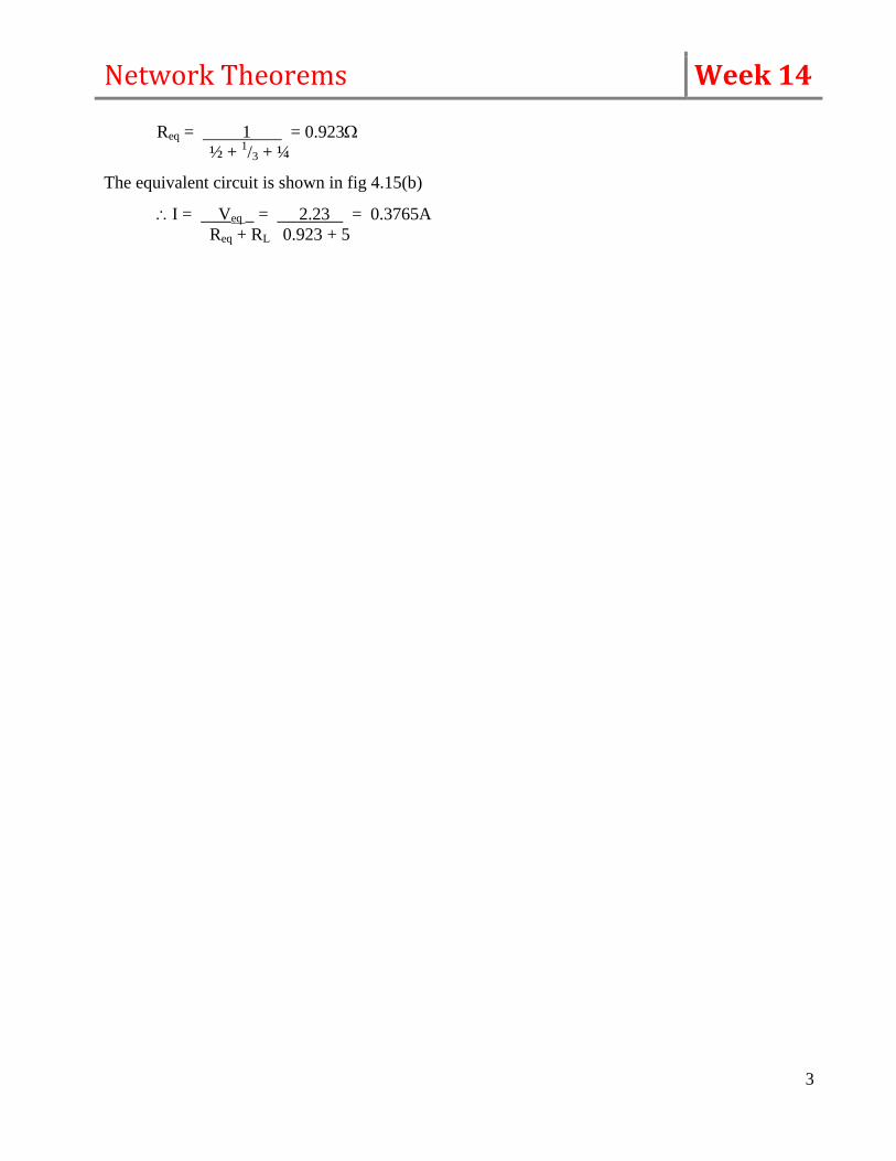
Req = 1 = 0.923
½ + 1/3 + ¼
The equivalent circuit is shown in fig 4.15(b)
I = Veq = 2.23 = 0.3765A
Req + RL 0.923 + 5
Network Theorems Week 15
1
At the end of this week, the students are expected to:
State Reciprocity theorem
Explain the basic principle of Reciprocity theorem
Solve network problems using Reciprocity theorem
4.12 RECIPROCITY THEOREM
This state that in any linear bilateral network , if a source of e.m.f E in any branch produces a
current I in any other branch, then the same e.m.f E acting in the second branch would be the same
current I in the first branch.
4.13 BASIC PRINCIPLE OF RECIPROCITY THEOREM
When applying the reciprocity theorem, the following principle must be followed:
1. The voltage sources is replaced by a short circuit in the original location
2. The polarity of the source in the new location is such that the current direction in that branch
remains unchanged.
4.14 SOLVED NETWORK PROBLEMS USING RECIPROCIUTY
THEOREM
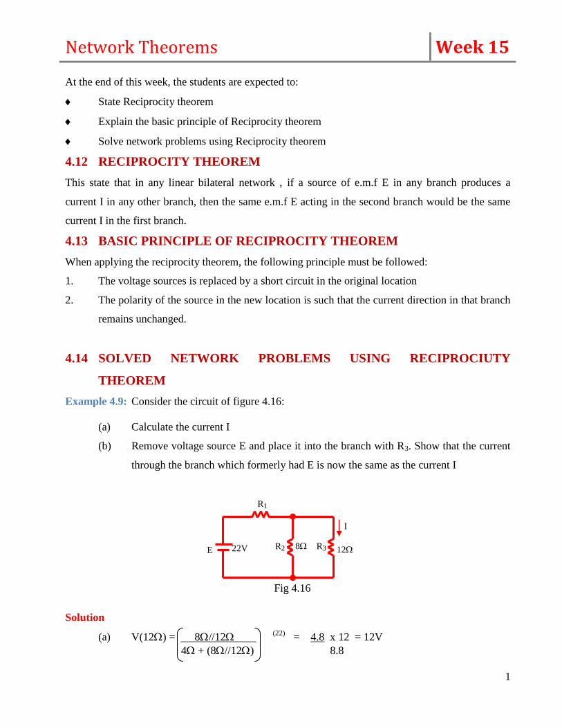
Example 4.9: Consider the circuit of figure 4.16:
(a) Calculate the current I
(b) Remove voltage source E and place it into the branch with R3. Show that the current
through the branch which formerly had E is now the same as the current I
Solution
(a) V(12) = 8//12 (22)
= 4.8 x 12 = 12V
4 + (8//12) 8.8
E
R1
R2 R3
I
22V 8 12
Fig 4.16
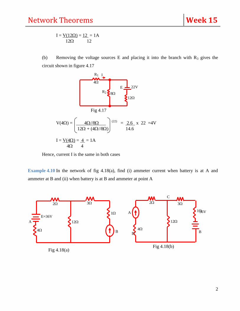
Network Theorems Week 15
2
I = V(12) = 12 = 1A
12 12
(b) Removing the voltage sources E and placing it into the branch with R3 gives the
circuit shown in figure 4.17
V(4) = 4//8 (22)
= 2.6 x 22 =4V
12 + (4//8) 14.6
I = V(4) = 4 = 1A
4 4
Hence, current I is the same in both cases
Example 4.10 In the network of fig 4.18(a), find (i) ammeter current when battery is at A and
ammeter at B and (ii) when battery is at B and ammeter at point A
E
R1
R2
I
22V
8 12
Fig 4.17
4
A
4
12
2 3
1
B
Fig 4.18(a)
E=36V A
12
2 3
1
B 4
C
Fig 4.18(b)
36V
D
Network Theorems Week 15
3
Solution
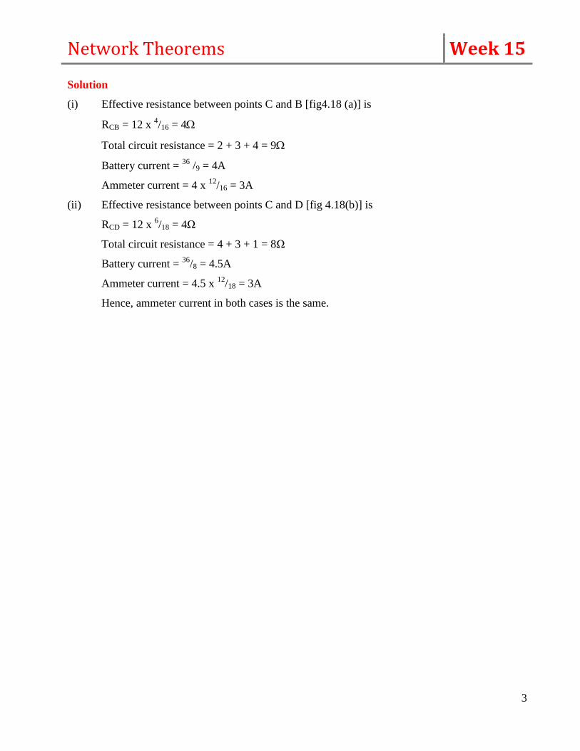
(i) Effective resistance between points C and B [fig4.18 (a)] is
RCB = 12 x 4/16 = 4
Total circuit resistance = 2 + 3 + 4 = 9
Battery current = 36
/9 = 4A
Ammeter current = 4 x 12
/16 = 3A
(ii) Effective resistance between points C and D [fig 4.18(b)] is
RCD = 12 x 6/18 = 4Ω
Total circuit resistance = 4 + 3 + 1 = 8Ω
Battery current = 36
/8 = 4.5A
Ammeter current = 4.5 x 12
/18 = 3A
Hence, ammeter current in both cases is the same.