Embed Size (px)
Citation preview
Microelectronics Reliability xxx (2015) xxx–xxx
MR-11554; No of Pages 4
Contents lists available at ScienceDirect
Microelectronics Reliability
j ourna l homepage: www.e lsev ie r .com/ locate /mr
Effects of thermal cycling on aluminum metallization of power diodes
M. Brincker ⁎, K.B. Pedersen, P.K. Kristensen, V.N. PopokDepartment of Physics and Nanotechnology, Aalborg University, Skjernvej 4A, DK-9220 Aalborg East, Denmark
⁎ Corresponding author.E-mail address: [email protected] (M. Brincker).
http://dx.doi.org/10.1016/j.microrel.2015.06.0050026-2714/© 2015 Elsevier Ltd. All rights reserved.
Please cite this article as: M. Brincker, et al.,(2015), http://dx.doi.org/10.1016/j.microrel.
a b s t r a c t
a r t i c l e i n f oArticle history:Received 25 May 2015Accepted 9 June 2015Available online xxxx
Keywords:Metallization degradationThermo-mechanical fatiguePassive thermal cyclingAluminum
Reconstruction of aluminummetallization on top of power electronic chips is a well-known wear out phenom-enonunder power cycling conditions. However, the origins of reconstruction are still under discussion. In the cur-rent study, a method for carrying out passive thermal cycling of power diodes in a controlled environment isdeveloped, thus eliminating possible contribution to degradation from electric current and humidity. The focusis centered on the structural changes in the top Al metallization layer of the power diodes, correlated with thechange of sheet resistance. Since the atmosphere is controlled and the device is not subjected to a current loadthe observed degradation of metallization and corresponding increase of resistance is purely induced bythermo-mechanical stress. A correlation between number of cycles, micro-structural evolution, and sheet resis-tance is found and conclusions on the dominant role of thermo-mechanical stresses are achieved. Additionally,proposals aremade on how the current thermal test setup can be further developed to study the role of corrosion.
© 2015 Elsevier Ltd. All rights reserved.
1. Introduction
In power electronic chips, Al metallization is often used as an inter-connect material for wire bonding, sintering etc. The thickness of themetallization is typically on sub-micrometer to micrometer scale andthe layer is deposited on top of silicon. Due to a mismatch of thermalexpansion coefficients of the Si/Al structure the aluminum is subjectedto thermo-mechanical stresses under thermal cycling which lead toreconstruction and degradation of the metallization [1]. Despite thesimplicity of this system, real origins of the degradation are not fullyunderstood and attract increased attention [2–4].
The reconstruction of the metallization is believed to occur as acomplex interplay between electrical effects such as electro-migrationand stress migration such as grain-boundary diffusion [5] as well asthermo-mechanical fatigue such as grain boundary sliding and plasticdeformation [1].
To investigatemetallization reconstruction in power electronic chipsa passive thermal cycling setup operating in a controlled atmosphere isconstructed. This approach is chosen to exclude current induced effectslike electro-migration. The thermal cycling setup is enclosed in an air-tight box that is continuously pumped with nitrogen which ensuresan atmosphere with low humidity and therefore limits corrosion.
2. Experimental procedure
All devices under test (DUT) are single unpackaged high powerInfineon diodes (100 A/1200 V). The diodes are 9 × 9 mm squares
Effects of thermal cycling on2015.06.005
with 3.4 μm thick Al metallization layer on the top. DUTs are subjectedto the thermal cycling and characterized using measurements ofsheet resistance and scanning electronmicroscopy (SEM) accompaniedby focused ion beam (FIB) milling to obtain cross-sections. SEM mea-surements are carried out using Zeis 1540XB system and standardprocedure.
2.1. Thermal cycling setup
The setup is based on a thermoelectric cooler (TEC). One side of theTEC is connected to a water-cooled Al block with constant temperature,while the other side is used for thermal cycling of the DUT. A current of3 A is supplied to the TEC until the diode surface reaches the desiredmaximum temperature, Tmax. This is measured with a thermocouplein direct contact with the metallization on one of the diodes. WhenTmax is reached, the current is reversed, such that the TEC rapidly coolsthe diodes down to the minimum temperature, Tmin, which constitutesa single cycle. The thermal cycling profile of the setup is shown in Fig. 1.Cycling is performed with a constant ΔT and constant TEC-current,while the current direction is modulated accordingly. By modulatingthe current amplitude together with the current direction, temperatureprofiles that differ from Fig. 1 and include dwell times and more closelyresemble typical operation conditions for DUT could be realized usingthe same setup. All DUTs are placed in direct contact with the TECwith no thermal compound, to avoid contamination of themetallizationduring handling and measurements. The temperature distributionacross the TEC is checked and it is found to be largely homogenouswith variations within ±2 °C in the center area where the DUTs areplaced. The entire thermal setup is encapsulated in a plastic enclosurethroughwhich a continuousflowof pure (99,999%) nitrogen is provided
aluminummetallization of power diodes, Microelectronics Reliability
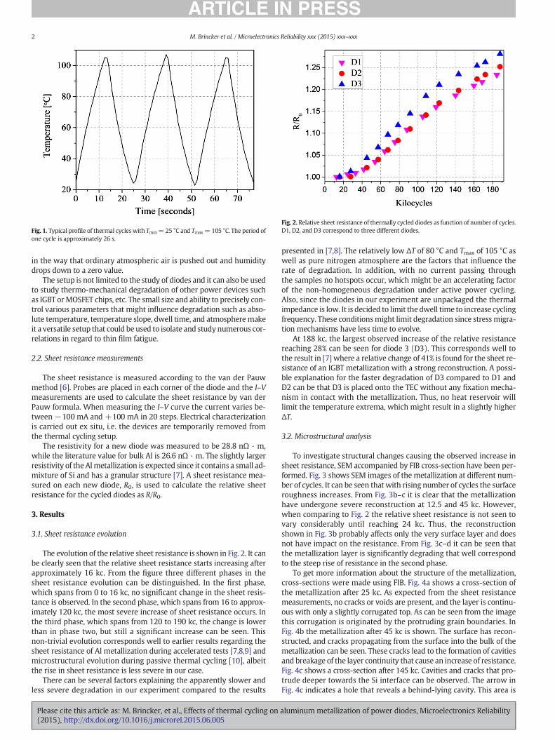
Fig. 1. Typical profile of thermal cycleswith Tmin= 25 °C and Tmax= 105 °C. The period ofone cycle is approximately 26 s.
Fig. 2. Relative sheet resistance of thermally cycled diodes as function of number of cycles.D1, D2, and D3 correspond to three different diodes.
2 M. Brincker et al. / Microelectronics Reliability xxx (2015) xxx–xxx
in the way that ordinary atmospheric air is pushed out and humiditydrops down to a zero value.
The setup is not limited to the study of diodes and it can also be usedto study thermo-mechanical degradation of other power devices suchas IGBT orMOSFET chips, etc. The small size and ability to precisely con-trol various parameters that might influence degradation such as abso-lute temperature, temperature slope, dwell time, and atmospheremakeit a versatile setup that could be used to isolate and study numerous cor-relations in regard to thin film fatigue.
2.2. Sheet resistance measurements
The sheet resistance is measured according to the van der Pauwmethod [6]. Probes are placed in each corner of the diode and the I–Vmeasurements are used to calculate the sheet resistance by van derPauw formula. When measuring the I–V curve the current varies be-tween−100 mA and +100 mA in 20 steps. Electrical characterizationis carried out ex situ, i.e. the devices are temporarily removed fromthe thermal cycling setup.
The resistivity for a new diode was measured to be 28.8 nΩ · m,while the literature value for bulk Al is 26.6 nΩ · m. The slightly largerresistivity of the Almetallization is expected since it contains a small ad-mixture of Si and has a granular structure [7]. A sheet resistance mea-sured on each new diode, R0, is used to calculate the relative sheetresistance for the cycled diodes as R/R0.
3. Results
3.1. Sheet resistance evolution
The evolution of the relative sheet resistance is shown in Fig. 2. It canbe clearly seen that the relative sheet resistance starts increasing afterapproximately 16 kc. From the figure three different phases in thesheet resistance evolution can be distinguished. In the first phase,which spans from 0 to 16 kc, no significant change in the sheet resis-tance is observed. In the second phase, which spans from 16 to approx-imately 120 kc, the most severe increase of sheet resistance occurs. Inthe third phase, which spans from 120 to 190 kc, the change is lowerthan in phase two, but still a significant increase can be seen. Thisnon-trivial evolution corresponds well to earlier results regarding thesheet resistance of Al metallization during accelerated tests [7,8,9] andmicrostructural evolution during passive thermal cycling [10], albeitthe rise in sheet resistance is less severe in our case.
There can be several factors explaining the apparently slower andless severe degradation in our experiment compared to the results
Please cite this article as: M. Brincker, et al., Effects of thermal cycling on(2015), http://dx.doi.org/10.1016/j.microrel.2015.06.005
presented in [7,8]. The relatively low ΔT of 80 °C and Tmax of 105 °C aswell as pure nitrogen atmosphere are the factors that influence therate of degradation. In addition, with no current passing throughthe samples no hotspots occur, which might be an accelerating factorof the non-homogeneous degradation under active power cycling.Also, since the diodes in our experiment are unpackaged the thermalimpedance is low. It is decided to limit the dwell time to increase cyclingfrequency. These conditionsmight limit degradation since stress migra-tion mechanisms have less time to evolve.
At 188 kc, the largest observed increase of the relative resistancereaching 28% can be seen for diode 3 (D3). This corresponds well tothe result in [7] where a relative change of 41% is found for the sheet re-sistance of an IGBT metallization with a strong reconstruction. A possi-ble explanation for the faster degradation of D3 compared to D1 andD2 can be that D3 is placed onto the TEC without any fixation mecha-nism in contact with the metallization. Thus, no heat reservoir willlimit the temperature extrema, which might result in a slightly higherΔT.
3.2. Microstructural analysis
To investigate structural changes causing the observed increase insheet resistance, SEM accompanied by FIB cross-section have been per-formed. Fig. 3 shows SEM images of the metallization at different num-ber of cycles. It can be seen that with rising number of cycles the surfaceroughness increases. From Fig. 3b–c it is clear that the metallizationhave undergone severe reconstruction at 12.5 and 45 kc. However,when comparing to Fig. 2 the relative sheet resistance is not seen tovary considerably until reaching 24 kc. Thus, the reconstructionshown in Fig. 3b probably affects only the very surface layer and doesnot have impact on the resistance. From Fig. 3c–d it can be seen thatthe metallization layer is significantly degrading that well correspondto the steep rise of resistance in the second phase.
To get more information about the structure of the metallization,cross-sections were made using FIB. Fig. 4a shows a cross-section ofthe metallization after 25 kc. As expected from the sheet resistancemeasurements, no cracks or voids are present, and the layer is continu-ous with only a slightly corrugated top. As can be seen from the imagethis corrugation is originated by the protruding grain boundaries. InFig. 4b the metallization after 45 kc is shown. The surface has recon-structed, and cracks propagating from the surface into the bulk of themetallization can be seen. These cracks lead to the formation of cavitiesand breakage of the layer continuity that cause an increase of resistance.Fig. 4c shows a cross-section after 145 kc. Cavities and cracks that pro-trude deeper towards the Si interface can be observed. The arrow inFig. 4c indicates a hole that reveals a behind-lying cavity. This area is
aluminummetallization of power diodes, Microelectronics Reliability
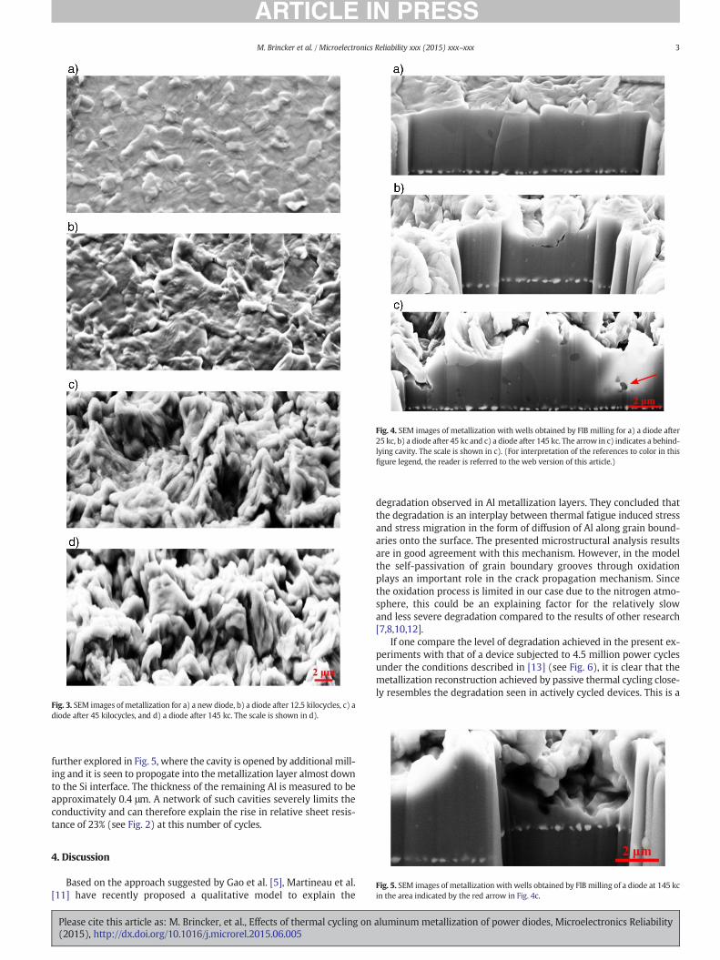
Fig. 4. SEM images of metallization with wells obtained by FIB milling for a) a diode after25 kc, b) a diode after 45 kc and c) a diode after 145 kc. The arrow in c) indicates a behind-lying cavity. The scale is shown in c). (For interpretation of the references to color in thisfigure legend, the reader is referred to the web version of this article.)
Fig. 3. SEM images ofmetallization for a) a new diode, b) a diode after 12.5 kilocycles, c) adiode after 45 kilocycles, and d) a diode after 145 kc. The scale is shown in d).
3M. Brincker et al. / Microelectronics Reliability xxx (2015) xxx–xxx
further explored in Fig. 5, where the cavity is opened by additional mill-ing and it is seen to propogate into themetallization layer almost downto the Si interface. The thickness of the remaining Al is measured to beapproximately 0.4 μm. A network of such cavities severely limits theconductivity and can therefore explain the rise in relative sheet resis-tance of 23% (see Fig. 2) at this number of cycles.
Fig. 5. SEM images of metallization with wells obtained by FIB milling of a diode at 145 kcin the area indicated by the red arrow in Fig. 4c.
4. Discussion
Based on the approach suggested by Gao et al. [5], Martineau et al.[11] have recently proposed a qualitative model to explain the
Please cite this article as: M. Brincker, et al., Effects of thermal cycling on(2015), http://dx.doi.org/10.1016/j.microrel.2015.06.005
degradation observed in Al metallization layers. They concluded thatthe degradation is an interplay between thermal fatigue induced stressand stress migration in the form of diffusion of Al along grain bound-aries onto the surface. The presented microstructural analysis resultsare in good agreement with this mechanism. However, in the modelthe self-passivation of grain boundary grooves through oxidationplays an important role in the crack propagation mechanism. Sincethe oxidation process is limited in our case due to the nitrogen atmo-sphere, this could be an explaining factor for the relatively slowand less severe degradation compared to the results of other research[7,8,10,12].
If one compare the level of degradation achieved in the present ex-periments with that of a device subjected to 4.5 million power cyclesunder the conditions described in [13] (see Fig. 6), it is clear that themetallization reconstruction achieved by passive thermal cycling close-ly resembles the degradation seen in actively cycled devices. This is a
aluminummetallization of power diodes, Microelectronics Reliability
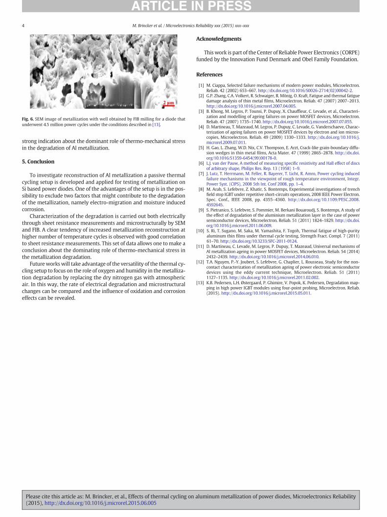
Fig. 6. SEM image of metallization with well obtained by FIB milling for a diode thatunderwent 4.5 million power cycles under the conditions described in [13].
4 M. Brincker et al. / Microelectronics Reliability xxx (2015) xxx–xxx
strong indication about the dominant role of thermo-mechanical stressin the degradation of Al metallization.
5. Conclusion
To investigate reconstruction of Al metallization a passive thermalcycling setup is developed and applied for testing of metallization onSi based power diodes. One of the advantages of the setup is in the pos-sibility to exclude two factors that might contribute to the degradationof the metallization, namely electro-migration and moisture inducedcorrosion.
Characterization of the degradation is carried out both electricallythrough sheet resistance measurements and microstructurally by SEMand FIB. A clear tendency of increased metallization reconstruction athigher number of temperature cycles is observed with good correlationto sheet resistancemeasurements. This set of data allows one tomake aconclusion about the dominating role of thermo-mechanical stress inthe metallization degradation.
Futureworkswill take advantage of the versatility of the thermal cy-cling setup to focus on the role of oxygen and humidity in themetalliza-tion degradation by replacing the dry nitrogen gas with atmosphericair. In this way, the rate of electrical degradation and microstructuralchanges can be compared and the influence of oxidation and corrosioneffects can be revealed.
Please cite this article as: M. Brincker, et al., Effects of thermal cycling on(2015), http://dx.doi.org/10.1016/j.microrel.2015.06.005
Acknowledgments
This work is part of the Center of Reliable Power Electronics (CORPE)funded by the Innovation Fund Denmark and Obel Family Foundation.
References
[1] M. Ciappa, Selected failure mechanisms of modern power modules, Microelectron.Reliab. 42 (2002) 653–667. http://dx.doi.org/10.1016/S0026-2714(02)00042-2.
[2] G.P. Zhang, C.A. Volkert, R. Schwaiger, R. Mönig, O. Kraft, Fatigue and thermal fatiguedamage analysis of thin metal films, Microelectron. Reliab. 47 (2007) 2007–2013.http://dx.doi.org/10.1016/j.microrel.2007.04.005.
[3] B. Khong, M. Legros, P. Tounsi, P. Dupuy, X. Chauffleur, C. Levade, et al., Characteri-zation and modelling of ageing failures on power MOSFET devices, Microelectron.Reliab. 47 (2007) 1735–1740. http://dx.doi.org/10.1016/j.microrel.2007.07.055.
[4] D. Martineau, T. Mazeaud, M. Legros, P. Dupuy, C. Levade, G. Vanderschaeve, Charac-terization of ageing failures on power MOSFET devices by electron and ion micros-copies, Microelectron. Reliab. 49 (2009) 1330–1333. http://dx.doi.org/10.1016/j.microrel.2009.07.011.
[5] H. Gao, L. Zhang, W.D. Nix, C.V. Thompson, E. Arzt, Crack-like grain-boundary diffu-sion wedges in thin metal films, Acta Mater. 47 (1999) 2865–2878. http://dx.doi.org/10.1016/S1359-6454(99)00178-0.
[6] L.J. van der Pauw, A method of measuring specific resistivity and Hall effect of discsof arbitrary shape, Philips Res. Rep. 13 (1958) 1–9.
[7] J. Lutz, T. Herrmann, M. Feller, R. Bayerer, T. Licht, R. Amro, Power cycling inducedfailure mechanisms in the viewpoint of rough temperature environment, Integr.Power Syst. (CIPS), 2008 5th Int. Conf 2008, pp. 1–4.
[8] M. Arab, S. Lefebvre, Z. Khatir, S. Bontemps, Experimental investigations of trenchfield stop IGBT under repetitive short-circuits operations, 2008 IEEE Power Electron.Spec. Conf., IEEE 2008, pp. 4355–4360. http://dx.doi.org/10.1109/PESC.2008.4592645.
[9] S. Pietranico, S. Lefebvre, S. Pommier, M. Berkani Bouaroudj, S. Bontemps, A study ofthe effect of degradation of the aluminium metallization layer in the case of powersemiconductor devices, Microelectron. Reliab. 51 (2011) 1824–1829. http://dx.doi.org/10.1016/j.microrel.2011.06.009.
[10] S. Ri, T. Sugano, M. Saka, M. Yamashita, F. Togoh, Thermal fatigue of high-purityaluminum thin films under thermal cycle testing, Strength Fract. Compl. 7 (2011)61–70. http://dx.doi.org/10.3233/SFC-2011-0124.
[11] D. Martineau, C. Levade, M. Legros, P. Dupuy, T. Mazeaud, Universal mechanisms ofAl metallization ageing in power MOSFET devices, Microelectron. Reliab. 54 (2014)2432–2439. http://dx.doi.org/10.1016/j.microrel.2014.06.010.
[12] T.A. Nguyen, P.-Y. Joubert, S. Lefebvre, G. Chaplier, L. Rousseau, Study for the non-contact characterization of metallization ageing of power electronic semiconductordevices using the eddy current technique, Microelectron. Reliab. 51 (2011)1127–1135. http://dx.doi.org/10.1016/j.microrel.2011.02.002.
[13] K.B. Pedersen, L.H. Østergaard, P. Ghimire, V. Popok, K. Pedersen, Degradation map-ping in high power IGBT modules using four-point probing, Microelectron. Reliab.(2015). http://dx.doi.org/10.1016/j.microrel.2015.05.011.
aluminummetallization of power diodes, Microelectronics Reliability