Embed Size (px)
Citation preview
ww.sciencedirect.com
i n t e r n a t i o n a l j o u r n a l o f h y d r o g e n en e r g y 3 9 ( 2 0 1 4 ) 1 0 8 6 1e1 0 8 6 9
Available online at w
ScienceDirect
journal homepage: www.elsevier .com/locate/he
Electrochemically etched triangular pore arrays onGaP and their photoelectrochemical propertiesfrom water oxidation
Changqing Zhu, Maojun Zheng*, Zuzhou Xiong, Hong Li, Wenzhong Shen
Key Laboratory of Artificial Structure and Quantum Control, Ministry of Education, Department of Physics and
Astronomy, Shanghai Jiao Tong University, Shanghai 200240, PR China
a r t i c l e i n f o
Article history:
Received 12 February 2014
Received in revised form
11 April 2014
Accepted 4 May 2014
Available online 3 June 2014
Keywords:
Triangular pore arrays
Photoelectrochemical performance
Photocatalytic water splitting
High-field electrochemical etching
* Corresponding author. Tel./fax: þ86 21 342E-mail address: [email protected] (M
http://dx.doi.org/10.1016/j.ijhydene.2014.05.00360-3199/Copyright © 2014, Hydrogen Ener
a b s t r a c t
Large-scale, triangular pore arrays on GaP were successfully prepared via a simple and
high-efficient approach of electrochemical etching under high field. The obtained ordered
porous GaP exhibited high performance in the photoelectrochemical (PEC) properties
compared with bulk GaP. The photocurrent of the porous GaP exceeded one order of
magnitude higher than that of bulk material under 0.1 V compared to the reversible
hydrogen electrode (RHE), which indicated the porous structure could enhance photo-
response and facilitate the separation of photo-induced carrier charges and their collec-
tion. The structure of triangular pore arrays cooperated with its depth determined the PEC
performance of GaP. The optimal etching depth was obtained via testing the PEC perfor-
mance. The hydrogen production from bulk GaP and its porous structure material were
also tested from water splitting. Upon the porous structure, significantly enhanced
hydrogen production has also been observed, which indicated that the porous GaP should
have important potential in photocatalytic water splitting.
Copyright © 2014, Hydrogen Energy Publications, LLC. Published by Elsevier Ltd. All rights
reserved.
Introduction
Energy harvested from sunlight offers a reliable approach to
solve the energy crisis. As the largest renewable energy
source, the solar energy would provide a great possibility to
solve the terawatt energy challenge. However, the sunlight is
daily and seasonal variability in nature. In order to obtain a
stable, constant energy flux, solar energy should be converted
into chemical energy that can be efficiently used, stored, and
transported upon the demand. An attractive approach is
02791.. Zheng).
22gy Publications, LLC. Publ
converting solar energy into high-energy chemical bonds,
such as splitting water into hydrogen by sunlight [1e4].
Theoretically, the efficiency of a single band gap system could
reach up to 17%, which was assumed a 0.8 V overpotential [5].
A higher theoretical efficiency has been predicted when two
semiconductors are coupled as the photoanode and photo-
cathode to minic natural photosynthesis [5,6].
The free energy change for the conversion of H2O molec-
ulars to H2 and O2 is 237.2 kJ/mol. According to the Nernst
equation, it corresponds to dE ¼ 1.23 V per electron trans-
ferred. Therefore, the theoretical minimum band gap for the
ished by Elsevier Ltd. All rights reserved.

i n t e rn a t i o n a l j o u r n a l o f h y d r o g e n en e r g y 3 9 ( 2 0 1 4 ) 1 0 8 6 1e1 0 8 6 910862
water splitting is 1.23 eV [1e4]. Compared to other available
semiconductors, GaP is a promising photoelectrode material
for the water splitting since its conduction band edge is higher
than the redox potential of Hþ/H2 [7e10]. However, the short
carrier diffusion length in GaP leads to excessive minority
carrier recombination, which limits the utilization of GaP as a
photoelectrode. In order to solve this problem, several groups
investigated nonplanar semiconductor heterojunction
[11e16]. Moreover, much interest has been focus on the uti-
lization of nanoarchitecture to solve this issue [17e19]. It has
been reported that the photogenerated charge collection effi-
ciencies of GaP photoelectrodes can be improved by adjusting
the nonplanar photoelectrode containing nanowire, macro-
pore, etc. [6,9,16]. Although the preparation of porous GaP has
been studied extensively [20e27], the application of porous
GaP onwater splitting is scarce. Price et al. pointed out that the
macroporous n-type GaP photoelectrodes could support both
large photovoltages and photocurrents [16].
In this report, high-field electrochemical etching (i.e. high
current density, 1400 mA cm�2) has been used to obtain
porous GaP with regular triangular pores in our system.
Through the photoelectrochemical test, including photo-
voltage, photocurrent and IeV curves, one can find that the
porous structure obviously improves the photo-
electrochemical performance, in comparison with the bulk
GaP. In addition, the porous GaP is much more productive
than bulk GaP for the light-induced water splitting process.
Experimental sections
Preparation of ordered porous GaP and characterization
Single crystalline n-GaP (111) wafer (300 mm thick) doped with
sulfur at concentration of 4 � 1017 cm�3 was obtained from
GRIM Electro-optic Materials Co., Ltd. Wafer was cut into
8 mm � 8 mm and degreased by successively sonicating in
acetone and ethanol. And then they were rinsed with the
deionized water and dried in a nitrogen stream. Indium films
were deposited on the sample back surface by direct current
magnetron sputtering for Ohmic contacts. Then high purity
silver paint was smeared on the In films in order to establish
an electric contact with a copper plate. The copper plate
except the samplewas paintedwith inert epoxy to ensure only
the sample contact with the electrolyte. Then the copper plate
with the sample was pressed in an O-ring of an electro-
chemical cell leaving the sample exposed to the electrolyte. A
two-electrode set-up was used for electrochemical etching.
The sample was used as the working electrode. The counter
electrode was graphite electrode. Etching of planar GaP was
performed in a mixture solution of 0.5 M HBr and 0.309 M
oxalic acid. Prior to etching, the solution was put into water
bath under 4 �C for 30 min. In order to explore the optimiza-
tion of the depth of the porous structure, the etching was
performed galvanostatically at 0.9 A for 15 s, 30 s, 45 s, and
60 s, with vigorous stirring.
The etched GaP samples exhibited dark yellow and there
was a compact irregular layer on the surfaces of them. The
next step was to remove the irregular layer. The etched GaP
samples were immersed in aqua regia (3:1 HCl/HNO3 by
volume) for 180 s. As a result, the porous GaP samples
were obtained and appeared bright yellow. Scanning elec-
tron microscopic analysis of these materials was conducted
with an FEI Sirion 200 scanning electron microscope (SEM).
The crystal structure and phase of the samples before and
after etching were determined by X-ray diffraction (XRD: D8
ADVANCE X-ray diffractometer, Bruker, Germany) with
Cu Ka radiation (1.54 Å). The reflectance spectrum of
porous GaP was measured by using a Lambda 750S
spectrometer (PerkineElmer) consisting of a deuterium and
tungsten-halogen lamp, photomultiplier, and integrating
sphere with 60 mm. The samples were placed at the end of
the sphere at normal incidence. The reflection measure-
ments on the triangular pore arrays are normalized by the
reflection of the bulk GaP to obtain the relative reflectance of
the porous GaP.
Photoelectrochemical tests
Photoelectrochemical analyses under white light illumina-
tion were conducted using an online acquisition system.
Photovoltage measurements of bulk GaP and porous GaP
electrodes were performed using a three-electrode
configuration, with GaP materials as the working electrode,
platinum gauze as the counter electrode, and saturated Ag/
AgCl as the reference electrode. A mixture solution of 0.35 M
Na2S and 0.25 M Na2SO3 was used as the electrolyte, and it
played a role of the photo-induced hole scavenger and its
pH was 13.35. An electrochemical workstation (PARSTAT
4000) instrument was used to measure open-circuit photo-
voltage characteristics of the electrode. The illuminated area
of the working electrode was 0.64 cm2. A 300 W Xe lamp
(SOLARDGE 700, Beijing Perfectlight Technology Co. Ltd,
China) was used as the light source. The power intensity of
the light was 400 mW cm�2, which was measured by Solar
Simulator Spectroradiometer (LS-100, EKO Instruments Co.,
Ltd, Japan).
The chronoamperometry measurement of Iet photo-
response was evaluated under the same illumination at an
applied potential of 0.1 V contrast to the RHE. The cur-
rentevoltage (IeV curves) was also obtained to indicate the
characteristics of the electrode with a scan rate of 0.1 V/s. The
measured potentials versus the Ag/AgCl reference electrode
were converted to the RHE scale through the following
calculation ERHE¼ EAg/AgClþ 0.059pHþ E0Ag/AgCl [28], E0Ag/AgCl is
the standard potential of Ag/AgCl at 25 �C (0.1976 V). For
incident photon to current efficiency (IPCE) measurement, the
monochromatic irradiation from a Xe lamp equipped with
bandpass filters (central wavelengths: 450 nm and 550 nm),
and the photocurrent was recorded at a constant bias 0.1 V vs.
RHE.
The apparatus for water splitting was a gas-closed circu-
lation system (Beijing Perfectlight Technology Co. Ltd,
LabSolar-IIIAG) including a vacuum line and a reaction cell
with a topwindow Pyrex cell and this system connectwith the
gas chromatograph (GC). The amount of evolved H2 was
analysed at the online gas chromatograph (Shanghai Tech-
comp Scientific Instrument Co. Ltd., D7900P) included MS-5A
column and a thermal conductivity detector (TCD), and N2
was the carrier gas.
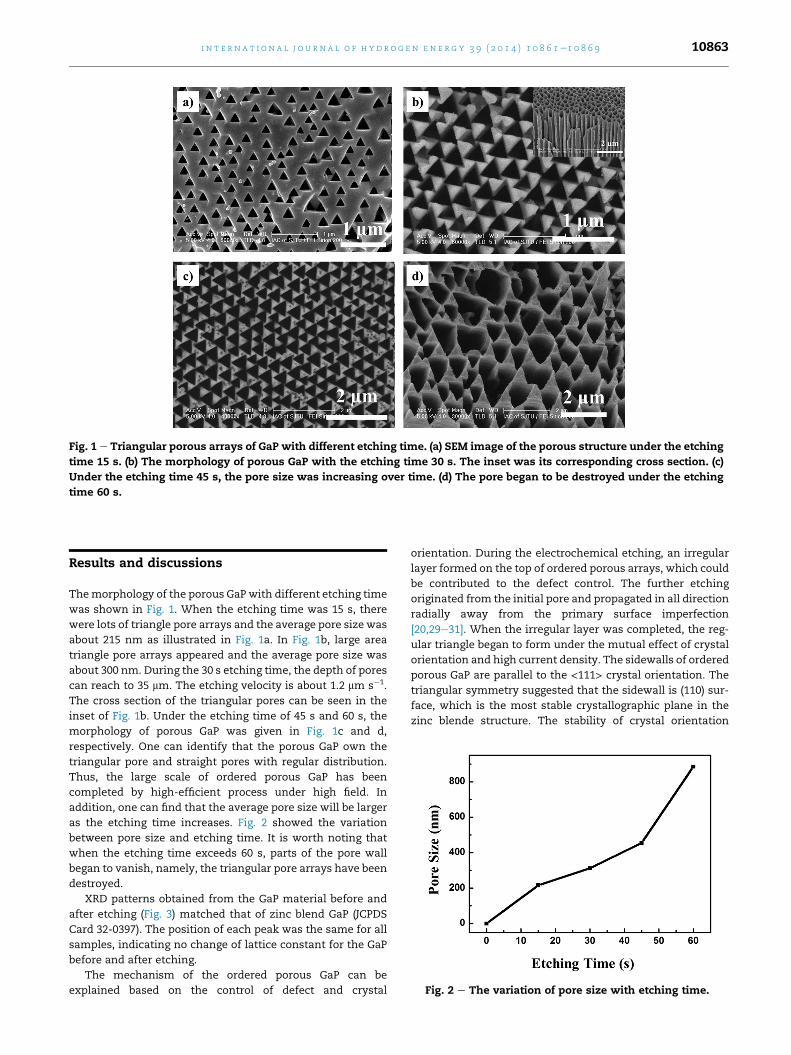
Fig. 1 e Triangular porous arrays of GaP with different etching time. (a) SEM image of the porous structure under the etching
time 15 s. (b) The morphology of porous GaP with the etching time 30 s. The inset was its corresponding cross section. (c)
Under the etching time 45 s, the pore size was increasing over time. (d) The pore began to be destroyed under the etching
time 60 s.
Fig. 2 e The variation of pore size with etching time.
i n t e r n a t i o n a l j o u r n a l o f h y d r o g e n en e r g y 3 9 ( 2 0 1 4 ) 1 0 8 6 1e1 0 8 6 9 10863
Results and discussions
Themorphology of the porous GaP with different etching time
was shown in Fig. 1. When the etching time was 15 s, there
were lots of triangle pore arrays and the average pore size was
about 215 nm as illustrated in Fig. 1a. In Fig. 1b, large area
triangle pore arrays appeared and the average pore size was
about 300 nm. During the 30 s etching time, the depth of pores
can reach to 35 mm. The etching velocity is about 1.2 mm s�1.
The cross section of the triangular pores can be seen in the
inset of Fig. 1b. Under the etching time of 45 s and 60 s, the
morphology of porous GaP was given in Fig. 1c and d,
respectively. One can identify that the porous GaP own the
triangular pore and straight pores with regular distribution.
Thus, the large scale of ordered porous GaP has been
completed by high-efficient process under high field. In
addition, one can find that the average pore size will be larger
as the etching time increases. Fig. 2 showed the variation
between pore size and etching time. It is worth noting that
when the etching time exceeds 60 s, parts of the pore wall
began to vanish, namely, the triangular pore arrays have been
destroyed.
XRD patterns obtained from the GaP material before and
after etching (Fig. 3) matched that of zinc blend GaP (JCPDS
Card 32-0397). The position of each peak was the same for all
samples, indicating no change of lattice constant for the GaP
before and after etching.
The mechanism of the ordered porous GaP can be
explained based on the control of defect and crystal
orientation. During the electrochemical etching, an irregular
layer formed on the top of ordered porous arrays, which could
be contributed to the defect control. The further etching
originated from the initial pore and propagated in all direction
radially away from the primary surface imperfection
[20,29e31]. When the irregular layer was completed, the reg-
ular triangle began to form under the mutual effect of crystal
orientation and high current density. The sidewalls of ordered
porous GaP are parallel to the <111> crystal orientation. The
triangular symmetry suggested that the sidewall is (110) sur-
face, which is the most stable crystallographic plane in the
zinc blende structure. The stability of crystal orientation
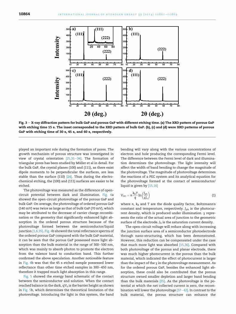
Fig. 3 e X-ray diffraction pattern for bulk GaP and porous GaP with different etching time. (a) The XRD pattern of porous GaP
with etching time 15 s. The inset corresponded to the XRD pattern of bulk GaP. (b), (c) and (d) were XRD patterns of porous
GaP with etching time of 30 s, 45 s, and 60 s, respectively.
i n t e rn a t i o n a l j o u r n a l o f h y d r o g e n en e r g y 3 9 ( 2 0 1 4 ) 1 0 8 6 1e1 0 8 6 910864
played an important role during the formation of pores. The
growth mechanism of porous structure was investigated in
view of crystal orientation [25,31e34]. The formation of
triangular pores has been studied by Muller et al in detail. For
the bulk GaP, the crystal planes (100) and (111), as there exist
dipole moments to be perpendicular the surfaces, are less
stable than the surface (110) [24]. Thus during the electro-
chemical etching, the (100) and (111) surfaces are easier to be
etched.
The photovoltage was measured as the difference of open-
circuit potential between dark and illumination. Fig. 4a
showed the open-circuit photovoltage of the porous GaP and
bulk GaP. On average, the photovoltage of ordered porous GaP
(140 mV) was twice as large as that of bulk GaP (70 mV), which
may be attributed to the decrease of carrier charge recombi-
nation or the geometry that significantly enhanced light ab-
sorption in the ordered porous structure because of the
photovoltage formed between the semiconductor/liquid
junction [1,6,35]. Fig. 4b showed the total reflectance spectra of
the ordered porous GaP compared with the bulk GaP material,
it can be seen that the porous GaP possessed more light ab-
sorption than the bulk material in the range of 300e500 nm,
which was mainly to absorb photon to promote the electron
from the valence band to conduction band. This further
confirmed the above speculation. Another noticeable feature
in Fig. 4b was that the 45 s etched sample possessed lower
reflectance than other time etched samples in 300e450 nm,
therefore it trapped much light absorption in this range.
Fig. 5 showed the energy band schematic of the contact
between the semiconductor and solution. When the contact
reached balance in the dark, qVb is the barrier height as shown
in Fig. 5b, which determines the theoretical limitation of the
photovoltage. Introducing the light in this system, the band
bending will vary along with the various concentrations of
electron and hole producing the corresponding Fermi level.
The difference between the Fermi level of dark and illumina-
tion determines the photovoltage. The light intensity will
affect the width of band bending to change the magnitude of
the photovoltage. The magnitude of photovoltage determines
the reactions of a PEC system and its analytical equation for
the photovoltage formed at the contact of semiconductor/
liquid is given by [15,16]
VOC ¼ nkBTq
ln
�JphcJs
�(1)
where n, kB and T are the diode quality factor, Boltzmann'sconstant and temperature, respectively. Jph is the photocur-
rent density, which is produced under illumination. c repre-
sents the ratio of the actual area of junction to the geometric
surface of the electrode. JS is the saturation current density.
The open-circuit voltage will reduce along with increasing
the junction surface area of a semiconductor photoelectrode
through nano-structuring, which has been demonstrated.
However, this reduction can be compensated under the case
that much more light was absorbed [15,36]. Compared with
both photovoltage of the porous and planar electrode, there
was much higher photocurrent in the porous than the bulk
material, which indicated the effect of photocurrent is larger
than the impact of the c in the photovoltagemeasurement. As
for the ordered porous GaP, besides the enhanced light ab-
sorption, these could also be contributed that the porous
structure owned smaller depletion and larger band bending
than the bulk materials [35]. As the photovoltage is the po-
tential at which the net collected current is zero, the recom-
binationwill lower the photovoltage [37e42]. In contrast to the
bulk material, the porous structure can enhance the
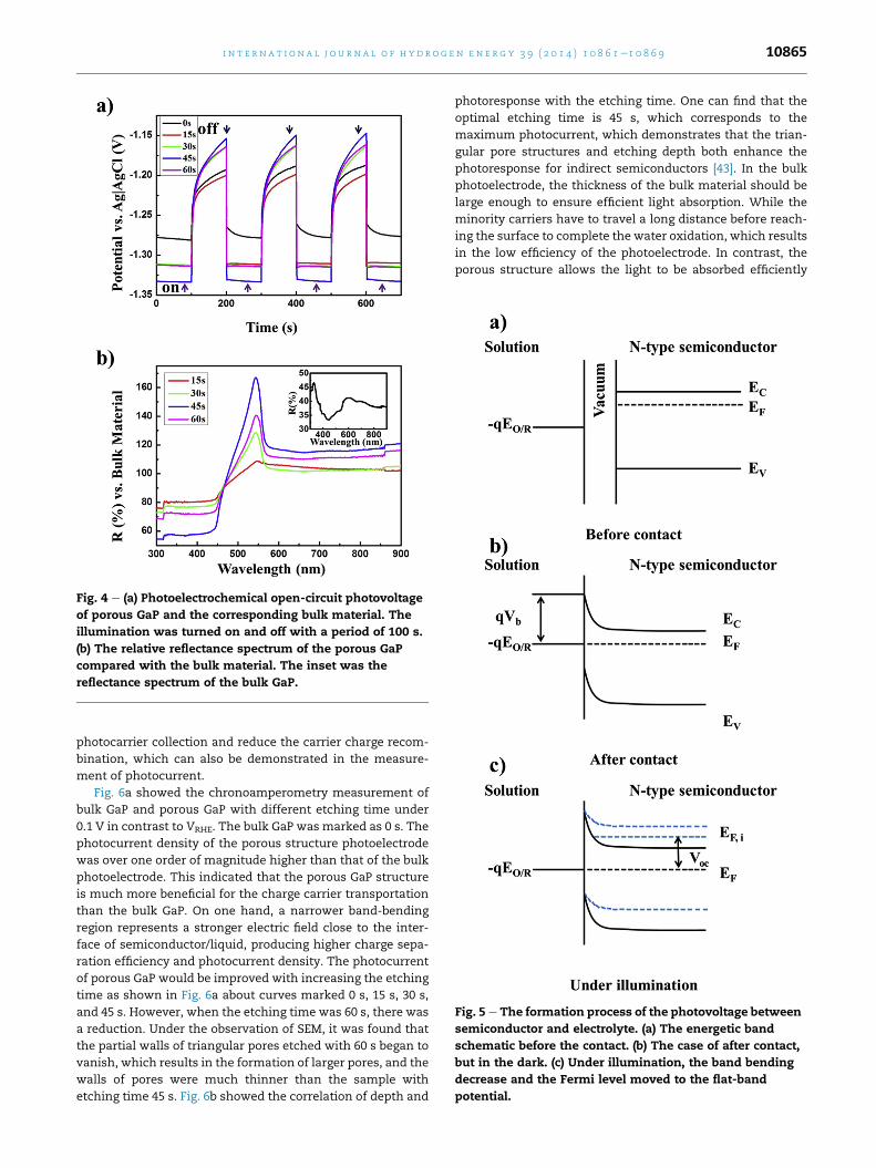
Fig. 4 e (a) Photoelectrochemical open-circuit photovoltage
of porous GaP and the corresponding bulk material. The
illumination was turned on and off with a period of 100 s.
(b) The relative reflectance spectrum of the porous GaP
compared with the bulk material. The inset was the
reflectance spectrum of the bulk GaP.
Fig. 5 e The formation process of the photovoltage between
semiconductor and electrolyte. (a) The energetic band
schematic before the contact. (b) The case of after contact,
but in the dark. (c) Under illumination, the band bending
decrease and the Fermi level moved to the flat-band
potential.
i n t e r n a t i o n a l j o u r n a l o f h y d r o g e n en e r g y 3 9 ( 2 0 1 4 ) 1 0 8 6 1e1 0 8 6 9 10865
photocarrier collection and reduce the carrier charge recom-
bination, which can also be demonstrated in the measure-
ment of photocurrent.
Fig. 6a showed the chronoamperometry measurement of
bulk GaP and porous GaP with different etching time under
0.1 V in contrast to VRHE. The bulk GaP was marked as 0 s. The
photocurrent density of the porous structure photoelectrode
was over one order of magnitude higher than that of the bulk
photoelectrode. This indicated that the porous GaP structure
is much more beneficial for the charge carrier transportation
than the bulk GaP. On one hand, a narrower band-bending
region represents a stronger electric field close to the inter-
face of semiconductor/liquid, producing higher charge sepa-
ration efficiency and photocurrent density. The photocurrent
of porous GaP would be improved with increasing the etching
time as shown in Fig. 6a about curves marked 0 s, 15 s, 30 s,
and 45 s. However, when the etching time was 60 s, there was
a reduction. Under the observation of SEM, it was found that
the partial walls of triangular pores etched with 60 s began to
vanish, which results in the formation of larger pores, and the
walls of pores were much thinner than the sample with
etching time 45 s. Fig. 6b showed the correlation of depth and
photoresponse with the etching time. One can find that the
optimal etching time is 45 s, which corresponds to the
maximum photocurrent, which demonstrates that the trian-
gular pore structures and etching depth both enhance the
photoresponse for indirect semiconductors [43]. In the bulk
photoelectrode, the thickness of the bulk material should be
large enough to ensure efficient light absorption. While the
minority carriers have to travel a long distance before reach-
ing the surface to complete the water oxidation, which results
in the low efficiency of the photoelectrode. In contrast, the
porous structure allows the light to be absorbed efficiently
Fig. 6 e (a) Chronoamperometry measurement (at 0.1 V vs. RHE) of porous GaP and the bulk material. The illumination was
turned on and off with a period of 60 s. The inset was the corresponding photoresponse of bulk GaP. (b) The correlation of
photocurrent (blue) and pore depth (yellow) with different etching time. The photocurrent data was measured at 0.1 V
versus RHE. (c) Time courses for the photocurrent of porous GaP etched time with 45 s. (d) Linear scan voltammetry
measurements of porous GaP and the corresponding bulk GaP. All experiments were performedwith themixture electrolyte
solution of 0.25 M Na2SO3 and 0.35 M Na2S (pH [ 13.35). (For interpretation of the references to colour in this figure legend,
the reader is referred to the web version of this article.)
i n t e rn a t i o n a l j o u r n a l o f h y d r o g e n en e r g y 3 9 ( 2 0 1 4 ) 1 0 8 6 1e1 0 8 6 910866
along their entire length, while holes can diffuse to the surface
over a short distance along the pore path. Large surface area
and efficient carrier collection is promoted to complete the
water splitting. Therefore, the ability to decouple the light
absorption length from theminority carrier diffusion length in
porous structure makes it potentially more efficient. As a
result, the porous GaP photoelectrode can be provided with
high performance for photoelectrochemical water splitting. At
the same time, the stability of porous structure was also
illustrated in Fig. 6c, and the sample with etching time 45 s as
an instance. The measurement condition of stability is the
same as in the photocurrent measurement as shown in
Fig. 6a. There is no obvious decrease of photocurrent, which
indicates that the triangular pore arrays are stable in the PEC
system.
In PECwater splitting, thewater oxidation involving a four-
electron transfer is normally more challenging than water
reduction. The water oxidation performance of n-GaP under
light irradiation was exhibited via photocurrent in Fig. 6d. The
enhancement factor, which was defined as the photocurrent
density of porous GaP over that of the bulk GaP [44], was over
10 under the 0.1 V compared to the RHE. It was noted that the
enhancement factor was also exceeded 10 in range of �1.0 to
�0.5 V compared to the Ag/AgCl reference electrode, as shown
in Fig. 6d. In the bulk n-GaP, holes, as the minority carriers,
have to traverse a long distance before reaching the bulk
surface to finish water oxidation, and most carriers have
finished recombination during this process, which attributes
the low efficiency of the photoelectrode. In comparison, the
porous structure can capture the light to absorb efficiently
along their entire depth, and holes can be effectively to collect
over a short distance to promote water oxidation. Therefore,
the porous photoelectrode displayed a much higher PEC ac-
tivity than the bulk photoelectrode. Moreover, the onset po-
tential of porous GaP is averagely less 50 mV than the bulk
material as shown in Fig. 6d inset. The IeV characteristics of
porous GaP and bulk GaP electrode exhibited similar behavior
as shown in Fig. 6a. The PEC performance of GaP improved as
the etching time increased, and it reached the optimal ca-
pacity under the etching time of 45 s. In order to further prove
this, IPCE was given in Fig. 7. The result suggested that the
porous structure was more effectively in enhancing the effi-
ciency. Optimizing the structure of the porous GaP could
further improve the efficiency of the porous electrode.
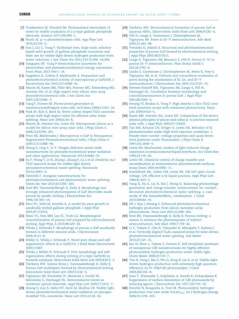
The capability of the pore arrays on GaP to drive hydrogen
production from water splitting under illumination at the
solution with hole scavenger was demonstrated. We choose
the sample etched with 30 s as an instance to compare with
bulk material in the hydrogen production from photocatalytic
water splitting. The mixture solution of 0.35 M Na2S and
0.25 M Na2SO3 was the sacrificial reagents in the hydrogen
production of photocatalyst. The mechanism of hydrogen
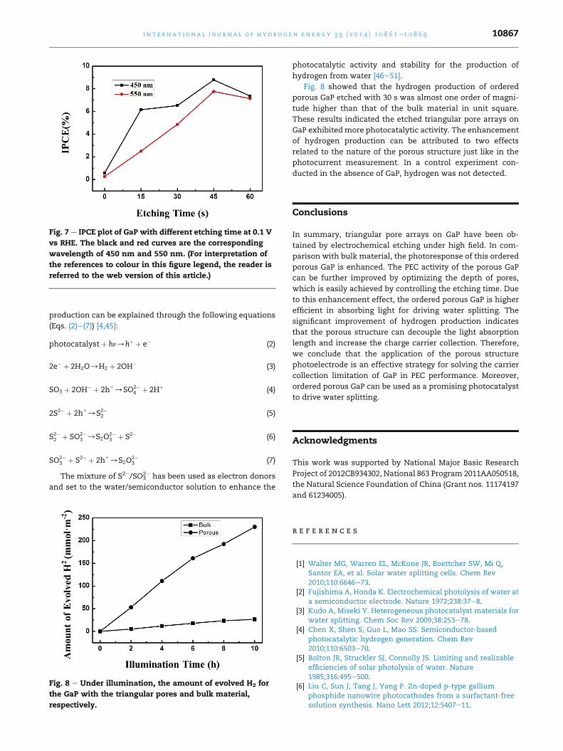
Fig. 7 e IPCE plot of GaP with different etching time at 0.1 V
vs RHE. The black and red curves are the corresponding
wavelength of 450 nm and 550 nm. (For interpretation of
the references to colour in this figure legend, the reader is
referred to the web version of this article.)
i n t e r n a t i o n a l j o u r n a l o f h y d r o g e n en e r g y 3 9 ( 2 0 1 4 ) 1 0 8 6 1e1 0 8 6 9 10867
production can be explained through the following equations
(Eqs. (2)e(7)) [4,45]:
photocatalystþ hn/hþ þ e� (2)
2e� þ 2H2O/H2 þ 2OH� (3)
SO3 þ 2OH� þ 2hþ/SO2�4 þ 2Hþ (4)
2S2� þ 2hþ/S2�2 (5)
S2�2 þ SO2�
3 /S2O2�3 þ S2� (6)
SO2�3 þ S2� þ 2hþ
/S2O2�3 (7)
The mixture of S2�/SO32� has been used as electron donors
and set to the water/semiconductor solution to enhance the
Fig. 8 e Under illumination, the amount of evolved H2 for
the GaP with the triangular pores and bulk material,
respectively.
photocatalytic activity and stability for the production of
hydrogen from water [46e51].
Fig. 8 showed that the hydrogen production of ordered
porous GaP etched with 30 s was almost one order of magni-
tude higher than that of the bulk material in unit square.
These results indicated the etched triangular pore arrays on
GaP exhibitedmore photocatalytic activity. The enhancement
of hydrogen production can be attributed to two effects
related to the nature of the porous structure just like in the
photocurrent measurement. In a control experiment con-
ducted in the absence of GaP, hydrogen was not detected.
Conclusions
In summary, triangular pore arrays on GaP have been ob-
tained by electrochemical etching under high field. In com-
parison with bulk material, the photoresponse of this ordered
porous GaP is enhanced. The PEC activity of the porous GaP
can be further improved by optimizing the depth of pores,
which is easily achieved by controlling the etching time. Due
to this enhancement effect, the ordered porous GaP is higher
efficient in absorbing light for driving water splitting. The
significant improvement of hydrogen production indicates
that the porous structure can decouple the light absorption
length and increase the charge carrier collection. Therefore,
we conclude that the application of the porous structure
photoelectrode is an effective strategy for solving the carrier
collection limitation of GaP in PEC performance. Moreover,
ordered porous GaP can be used as a promising photocatalyst
to drive water splitting.
Acknowledgments
This work was supported by National Major Basic Research
Project of 2012CB934302, National 863 Program 2011AA050518,
the Natural Science Foundation of China (Grant nos. 11174197
and 61234005).
r e f e r e n c e s
[1] Walter MG, Warren EL, McKone JR, Boettcher SW, Mi Q,Santor EA, et al. Solar water splitting cells. Chem Rev2010;110:6646e73.
[2] Fujishima A, Honda K. Electrochemical photolysis of water ata semiconductor electrode. Nature 1972;238:37e8.
[3] Kudo A, Miseki Y. Heterogeneous photocatalyst materials forwater splitting. Chem Soc Rev 2009;38:253e78.
[4] Chen X, Shen S, Guo L, Mao SS. Semiconductor-basedphotocatalytic hydrogen generation. Chem Rev2010;110:6503e70.
[5] Bolton JR, Struckler SJ, Connolly JS. Limiting and realizableefficiencies of solar photolysis of water. Nature1985;316:495e500.
[6] Liu C, Sun J, Tang J, Yang P. Zn-doped p-type galliumphosphide nanowire photocathodes from a surfactant-freesolution synthesis. Nano Lett 2012;12:5407e11.
i n t e rn a t i o n a l j o u r n a l o f h y d r o g e n en e r g y 3 9 ( 2 0 1 4 ) 1 0 8 6 1e1 0 8 6 910868
[7] Tomkiewicz M, Woodall JM. Photoassisted electrolysis ofwater by visible irradiation of a p-type gallium phosphideelectrode. Science 1977;196:990e1.
[8] Nozik AJ. pen photoelectrolysis cells. App Phys Lett1976;29:150e3.
[9] Sun J, Liu C, Yang P. Surfactant-free, large-scale, solution-liquid-solid growth of gallium phosphide nanowires andtheir use for visible-light-driven hydrogen production fromwater reduction. J Am Chem Soc 2011;133:19,306e19,309.
[10] Dasgupta NP. Yang P Semiconductor nanowires forphotovoltaic and photoelectrochemical energy conversion.Front Phys; 2013 Feb:1e14.
[11] Hagedorn K, Collins S, Maldonado S. Preparation andphotoelectrochemical activity of macroporous p-GaP(100). JElectrochem Soc 2010;157:D588e92.
[12] Maiolo JR, Kayes BM, Filler MA, Putnam MC, Kelzenberg MD,Atwater HA, et al. High aspect ratio silicon wire arrayphotoelectrochemical cells. J Am Chem Soc2007;129:12346e7.
[13] Yang F, Forrest SR. Photocurrent generation innanostructuredOrganic solar cells. ACS Nano 2008;2:1022e32.
[14] Park JH, Kim S, Bard AJ. Novel carbon-doped TiO2 nanotubearrays with high aspect ratios for efficient solar watersplitting. Nano Lett 2006;6:24e8.
[15] Maiolo JR, Atwater HA, Lewis NS. Macroporous silicon as amodel for silicon wire array solar cells. J Phys Chem C2008;112:6194e201.
[16] Price MJ, Maldonado J. Macroporous n-GaP in NonaqueousRegenerative Photoelectrochemical Cells. J Phys Chem C2009;113:11988e94.
[17] Wang G, Ling Y, Li Y. Oxygen-deficient metal oxidenanostructures for photoelectrochemical water oxidationand other applications. Nanoscale 2012;4:6682e91.
[18] Su F, Wang T, Lv R, Zhang J, Zhang P, Lu J, et al. Dendritic Au/TiO2 nanorod arrays for visible-light drivenphotoelectrochemical water splitting. Nanoscale2013;5:9001e9.
[19] Osterloh F. Inorganic nanostructures forphotoelectrochemical and photocatalytic water splitting.Chem Soc Rev 2013;42:2294e320.
[20] Ern�e BH, Vanmaekelbergh D, Kelly JJ. Morphology andstrongly enhanced photoresponse of GaP electrodes madeporous by anodic etching. J Electrochem Soc1996;143:305e14.
[21] Ricci PC, Salis M, Anedda A. A model for pore growth inanodically etched gallium phosphide. J Appl Phys2005;97:113522.
[22] Shen YC, Hon MH, Leu IC, Teoh LG. Morphologicalcharacterization of porous GaP prepared by electrochemicaletching. Appl Phys A 2010;98:429e34.
[23] Wloka J, Schmuki P. Morphology of porous n-GaP anodicallyformed in different mineral acids. J Electroceram2006;16:23e8.
[24] Muller K, Wloka J, Schmuki P. Novel pore shape and self-organization effects in n-GaP(111). J Solid State Electrochem2009;13:807.
[25] Wloka J, Muller K, Schmuki P. Pore morphology and self-organization effects during etching of n-type GaP(100) inbromide solutions. Eletrochem Solid-State Lett 2005;8:B72e5.
[26] Tjerkstra RW, G�omez Rivas J, Vanmaekelbergh D, Kelly JJ.Porous GaP multilayers formed by electrochemical etching.Eletrochem Solid-State Lett 2002;5:G32e5.
[27] Tiginyanu IM, Kravetsky IV, Monecke J, Cordts W,Marowsky G, Hartnagel HL. Semiconductor sieves asnonlinear optical materials. Appl Phys Lett 2000;77:2415e7.
[28] Hoang S, Guo S, Hahn NT, Bard AJ, Mullins CB. Visible lightdriven photoelectrochemical water oxidation on nitrogen-modified TiO2 nanowires. Nano Lett 2012;12:26e32.
[29] Tjerkstra RW. Electrochemical formation of porous GaP inaqueous HNO3. Electrochem Solid-State Lett 2006;9:C81e4.
[30] F€oll H, Langa S, Carstensen J, Christophersen M,Tiginyanu IM. Pores in IIIeV semiconductors. Adv Matt2003;15:183e98.
[31] Tomioka K, Adachi S. Structural and photoluminescenceproperties of porous GaP formed by electrochemical etching.J Appl Phys 2005;98:073511.
[32] Langa S, Tiginyanu IM, Monaico E, F€oll H. Porous IIeVI vs.porous IIIeV semiconductors. Phys Status Solidi C2011;8:1792e6.
[33] Landa S, Carstensen J, Christophersen M, Steen K, Frey S,Tiginyanu IM, et al. Uniform and nonuniform nucleation ofpores during the anodization of Si, Ge, and IIIeVsemiconductors. J Electrochem Soc 2005;152:C525e31.
[34] Stevens-Kalceff MA, Tiginyanu IM, Langa S, F€oll H,Hartnagel HL. Correlation between morphology andcathodoluminescence in porous GaP. J Appl Phys2001;89:2560e5.
[35] Hwang YJ, Boukai A, Yang P. High density n-Si/n-TiO2 core/shell nanowire arrays with enhanced photoactivity. NanoLett 2009;9:410e5.
[36] Kayes BM, Atwater HA, Lewis NS. Comparison of the devicephysics principles of planar and radial pen junction nanorodsolar cells. J Appl Phys 2005;97:114302.
[37] Tan MX, Kenyon CN, Kruger O, Lewis NS. Behavior of Siphotoelectrodes under high level injection conditions. 1.Steady-state current�voltage properties and quasi-fermilevel positions under Illumination. J Phys Chem B1997;101:2830e9.
[38] Lewis NS. Mechanistic studies of light-induced chargeseparation at semiconductor/liquid interfaces. Acc Chem Res1990;23:176e83.
[39] Lewis NS. Chemical control of charge transfer andrecombination at semiconductor photoelectrode surfaces.Inorg Chem 2005;44:6900e11.
[40] Rosenbluth ML, Lieber CM, Lewis NS. 630 mV open circuitvoltage, 12% efficient n-Si liquid junction. Appl Phys Lett1984;45:423e5.
[41] Yang X, Du C, Liu R, Xie J, Wang D. Balancing photovoltagegeneration and charge-transfer enhancement for catalyst-decorated photoelectrochemical water splitting: a casestudy of the hematite/MnOx combination. J Catal2013;304:86e91.
[42] Oh I, Kye J, Hwang S. Enhanced photoelectrochemicalhydrogen production from silicon nanowire arrayphotocathode. Nano Lett 2012;12:298e302.
[43] Ern�e BH, Vanmaekelbergh D, Kelly JJ. Porous etching: ameans to enhance the photoresponse of indirectsemiconductors. Adv Matt 1995;7:739e42.
[44] Li Y, Takata T, Cha D, Takanabe K, Minegishi T, Kubota J,et al. Vertically aligned Ta3N5 nanorod arrays for solar-drivenphotoelectrochemical water splitting. Adv Mater2013;25:125e31.
[45] Bao N, Shen L, Takata T, Domen K. Self-templated synthesisof nanoporous CdS nanostructures for highly efficientphotocatalytic hydrogen production under visible light.Chem Mater 2008;20:110e7.
[46] Yan H, Yang J, Ma G, Wu G, Zong X, Lei Z, et al. Visible-light-driven hydrogen production with extremely high quantumefficiency on PtePdS/CdS photocatalyst. J Catal2009;266:165e8.
[47] Inue T, Watanabe T, Fujishima A, Honda K, Kohayakawa K.Suppression of surface dissolution of CdS photoanode byreducing agents. J Electrochem Soc 1977;124:719e22.
[48] Koriche N, Bouguelia A, Trari M. Photocatalytic hydrogenproduction over new oxide CuLaO2.62. Int J Hydrogen Energy2006;31:1196e203.

i n t e r n a t i o n a l j o u r n a l o f h y d r o g e n en e r g y 3 9 ( 2 0 1 4 ) 1 0 8 6 1e1 0 8 6 9 10869
[49] Shen S, Guo L, Chen X, Ren F, Mao SS. Effect of Ag2S on solar-driven photocatalytic hydrogen evolution of nanostructuredCdS. Int J Hydrogen Energy 2010;35:7110e5.
[50] Zhang K, Jing D, Chen Q, Guo L. Influence of Sr-doping on thephotocatalytic activities of CdSeZnS solid solutionphotocatalysts. Int J Hydrogen Energy 2010;35:2048e57.
[51] Xu M, Zai J, Yuan Y, Qian X. Band gap-tunable(CuIn)xZn2(1�x)S2 solid solutions: preparation and efficientphotocatalytic hydrogen production from water undervisible light without noble metals. J Mater Chem2012;22:23,929e23,934.

![arXiv:1902.01369v1 [cond-mat.mtrl-sci] 4 Feb 2019 · Tungsten wire is etched electrochemically with 3 mol/L aqueous NaOH via the lamellae drop-o technique [17]: A thin lm of the electrolyte](https://img.pdfslide.net/doc/110x75/609bed314921d8463535303c/arxiv190201369v1-cond-matmtrl-sci-4-feb-2019-tungsten-wire-is-etched-electrochemically.jpg)