Embed Size (px)
Citation preview
ELECTROSTATIC DISCHARGE FOR SYSYEM
ON CHIP APPLICATIONS
By
CHERYL SHE SIEW YUET
A Dissertation submitted for partial fulfilment of the
requirement for the degree of Master of Science
(Microelectronic Engineering)
AUGUST 2017

ii
ACKNOWLEDGEMENT
Firstly, I would like to take this opportunity to express my gratitude and thanks
to my supervisor, Prof. Madya Ir. Dr. Arjuna Marzuki from the School of Electrical
and Electronics Engineering, University Science of Malaysia, for his relentless
guidance and courage throughout the undertaking of this research project. Many
constructive feedbacks and advices given were much appreciated, besides sacrificing
his valuable time travelling to my company which helped to make this research run
smoothly.
Thanks for the supports by USM Engineering Faculty on the sharing talks and
writing workshops to help on improving our thesis writing skills. In addition, special
thanks to Usains Holdings Sdn. Bhd. who partnered with USM in hosting this master
program. Thank you for the logistics planning and curriculum arrangements.
Nevertheless, Intel Technology (M) Sdn. Bhd for the data analysis tools namely JMP
to analyze the leakage measurement for before and after stress qualification across
every zapping. Moreover, analyzed on the leakage measurement degradation or delta
post ESD stress.
Finally, I would like to express my gratitude to my beloved family and friends
or fellow course mates who have supported or encouraged me throughout the
undertaking of this master program in MSc in Microelectronic Engineering in
University Science of Malaysia.
iii
TABLE OF CONTENTS
ACKNOWLEDGEMENT ......................................................................................... ii
ABSTRAK.................................................................................................................. vi
ABSTRACT .............................................................................................................. vii
LIST OF FIGURES ................................................................................................viii
LIST OF TABLES ..................................................................................................... x
LIST OF ABBREVIATION .................................................................................... xii
INTRODUCTION......................................................................... 1
1.0 Chapter Overview .......................................................................................... 1
1.1 Background .................................................................................................... 1
1.2 Importance and Challenges of Technology Scaling on ESD ........................ 3
1.3 Problem Statement ......................................................................................... 6
1.4 Research Objective ........................................................................................ 7
1.5 Research Scopes ............................................................................................ 8
1.6 Thesis Outline ................................................................................................ 8
LITERATURE REVIEW ............................................................ 9
2.0 Chapter Overview .......................................................................................... 9
2.1 Basic of Electrostatic Discharge Testing Model ........................................... 9
2.1.1 Human Body Charge (HBM) ............................................................... 11
2.1.2 Charged Device Model (CDM) ............................................................ 15
2.1.3 HBM and CDM Failure Criteria .......................................................... 18
2.2 ESD JEDEC Test Standard.......................................................................... 18
iv
2.2.1 HBM JEDEC Standard......................................................................... 19
2.2.2 CDM JEDEC Standard......................................................................... 23
2.3 ESD in Technology Scaling ........................................................................ 25
2.3.1 Impact of Technology Scaling in ESD Test ......................................... 26
2.3.2 Concept of Leakage Current ................................................................ 27
2.4 Data Analysis by JMP Statistic Tools ......................................................... 30
2.5 Summary ...................................................................................................... 31
METHODOLOGY ..................................................................... 32
3.0 Chapter Overview ........................................................................................ 32
3.1 ESD Experiment Planning on 14nm and 22nm ........................................... 34
3.2 Preliminary Preparation and Setup for ESD ................................................ 37
3.2.1 Pin Combinations for HBM ................................................................. 37
3.2.2 Pin Definitions for CDM ...................................................................... 39
3.2.3 HBM Process Flow .............................................................................. 41
3.2.4 CDM Process Flow .............................................................................. 44
3.3 DOE Strategy Method for ESD ................................................................... 46
3.3.1 DOE Method Correspond Research Objectives ................................... 46
3.3.2 HBM Testing Flow for 14nm and 22nm .............................................. 48
3.3.3 CDM Testing Flow for 14nm and 22nm .............................................. 51
3.3.4 Peak Current Cumulative Zap (DOE 4) ............................................... 52
3.4 ESD Failure Disposition Methodology ....................................................... 54
3.5 Summary ...................................................................................................... 55
RESULTS AND DISCUSSION ................................................. 56
4.0 Chapter Overview ....................................................................................... 56
4.1 DOE 1: HBM Stress Result ......................................................................... 56
4.2 DOE 2 and DOE 3 Result for CDM Methodology ..................................... 63

v
4.2.1 DOE 2: Positive Polarity CDM Stress Result ...................................... 63
4.2.2 DOE 3: Negative Polarity CDM Stress Result..................................... 67
4.3 DOE 4: Peak Current Analysis to Determine CDM Stress Voltage............ 72
4.4 Summary ...................................................................................................... 75
CONCLUSION AND FUTURE WORK .................................. 77
5.1 Conclusion ................................................................................................... 77
5.2 Future Works ............................................................................................... 78
REFERENCES ......................................................................................................... 79
APPENDIX A: .......................................................................................................... 85
APPENDIX B: .......................................................................................................... 86
APPENDIX C: .......................................................................................................... 87
APPENDIX D: .......................................................................................................... 88
APPENDIX E: .......................................................................................................... 89

vi
ABSTRAK
Pelepasan elektrostatik (ESD) tahap komponen litar masih kekal semenjak dua
dekad, jika dibandingkan dengan teknologi silikon yang telah menunjukkan
perkembangan yang pesat dalam kaedah kawalan ESD. Piawaian ESD JEDEC
memainkan peranan penting dalam penentuan tahap tekanan ESD dalam industri
semikonduktor dan diaplikasikan ke atas semua produk yang di mana spesifikasinya
bercirikan kaedah ujian ESD, prosedur dan penilaian, serta mengklasifikasikan model
caj tubuh badan (HBM) yang sensitif pada komponen dan model peranti caj (CDM)
yang sensitiviti terhadap dicaj. Piawai ini sememangnya kekurangan dalam penentuan
tekanan voltan maximum. Namun, terdapat ruang untuk penambahbaikan garis
panduan apabila melakukan persediaan awal untuk gabungan pin bagi ujian HBM.
Matlamat tesis ini adalah untuk mempertingkatkan metodologi ESD secara optimum
dengan rujukan piawai peruntukan kumpulan pin JEDEC dalam degradasi kebocoran
arus semasa tekanan untuk mengukur fungsi produk. Perubahan model ke tahap
sasaran tekanan ESD yang lebih sahih dan selamat telah disarankan, berdasarkan data
yang dikumpul daripada 14nm dan 22nm dengan menggunakan proses peranti
teknologi yang berbeza di mana sebahagian data digunakan untuk menganggar
ketepatan piawai JEDEC JS001 dan keperluan JS002 dalam peringkat komponen ESD
untuk HBM dan CDM masing-masing. Keberkesanan dalam untuk ukuran analisis
data untuk peningkatan arus bocor sebelum dan selepas ujian ESD dengan
menggunakan statistik JMP telah menjimatkan masa analitik. Hasil kajian ini juga
menunjukkan bahawa data yang dikumpul melalui ujian CDM pada 14nm dan 22nm
adalah lebih tepat dalam ramalan voltan tahanan berbandingkan kaedah puncak
semasa sejurus disebabkan oleh kegagalan pin terhadap voltan yang ditekankan.

vii
ABSTRACT
Integrated Circuit (IC) component level Electrostatic Discharge (ESD)
requisites have stayed constant essentially for past two decades, having said so since
the silicon technologies showing rapid advanced and efficacious control methods have
prodigiously amended as well as improved. ESD standard JEDEC requirements has
been part of success criteria on determine the ESD stress level in semiconductor
industry. The standards applied across all product where its specification define for
ESD test method, procedure, evaluation and classifying Human Body Model (HBM)
a ESD model sensitive on component and ESD sensitivity to charge namely Charged
Device Model (CDM). Apparently, the main gaps for this industrial standard missing
of defining the withstand ESD stress voltage and recommended step test. Nevertheless,
there is room of improvement to recommend guideline for when performing
preliminary setup on pin combination for HBM test. In this thesis, will recommend a
model change to more authentic but safe ESD stress target levels predicated on actual
field data accumulated from 14nm and 22nm differences technology process devices
as part of data for the learning on estimation the accuracy of the standards JEDEC
JS001 and JS002 requirements on HBM and CDM respectively. Nonetheless, a much
effective and time saving way established for data analysis of measurement leakage
current increase before and after ESD test using JMP statistics tool on 14nm and 22nm
small package devices. Driving to the standardization the new guideline for HBM
successfully established. Lastly, the result of this research demonstrates the actual
CDM test collected data on 14nm and 22nm more accurate on predicting the withstand
voltage compare the peak current methodology.

viii
LIST OF FIGURES
Figure 1.1: Illustrated RC network for HBM [2][3]..................................................... 2
Figure 1.2: CDM setup (left) and effective capacitor network (right) [2][4] ............... 3
Figure 2.1: Human body cause by electric discharge on a DUT and HBM Equivalent
circuit [10] .................................................................................................................. 11
Figure 2.2: MK4 Tester for HBM Stress Test [10] .................................................... 13
Figure 2.3 Example of initial IV cure trace with ± 10% reference point [10] ........... 15
Figure 2.4 Show the CDM mechanism on a DUT [10] ............................................. 16
Figure 2.5: Orion2 Tester for CDM Stress Test [10] ................................................. 17
Figure 2.6: Simplified HBM Simulator Load [4] ....................................................... 20
Figure 2.7: CDM Current versus time waveform [1] ................................................. 25
Figure 2.8: Impact of Technology Scaling on ESD Design Window [9] .................. 26
Figure 2.9: Proposed ESD Qualification [11] ............................................................ 27
Figure 2.10: Single Pin Test Leakage [12] ................................................................. 29
Figure 2.11: Pin to Pin Leakage [12] ......................................................................... 29
Figure 3.1: The Research Activities Flow .................................................................. 33
Figure 3.2: Quick Overview of ESD Test Flow ......................................................... 36
Figure 3.3: Pre-work on Pin Categories for HBM Testing ........................................ 38
Figure 3.4: Pre-work on Pin Groupings for HBM Testing ........................................ 39
Figure 3.5: Pre-work on Pin Categories to obtain pin definition for CDM Testing .. 41
Figure 3.6: Represented the HBM Process Flow [4] ................................................. 43
Figure 3.7: Represented the CDM Process Flow [1] ................................................. 45
Figure 3.8: HBM Testing Flowchart for 14nm and 22nm technology SOC devices . 50
Figure 3.9: CDM Testing Flowchart for 14nm and 22nm technology SOC devices . 52
Figure 3.10: CDM Voltage for 6A Ipeak for both polarity ........................................ 54

ix
Figure 3.11: ESD Failure Disposition Flow ............................................................... 55
Figure 4.1: Show the delta of leakage current after ESD Research Activities Flow . 59
Figure 4.2: Unpowered Curve Trace for Pin 1 on Product A .................................... 60
Figure 4.3: Show the delta of leakage current after positive CDM............................ 65
Figure 4.4: Delta leakage current for Product A (22nm) after positive CDM ........... 66
Figure 4.5: Delta leakage current for Product B and C (14nm) after positive CDM . 67
Figure 4.6: Show the delta of leakage current after negative CDM ........................... 69
Figure 4.7: Delta leakage current for Product A (22nm) after negative CDM .......... 70
Figure 4.8: Delta leakage current for Product B and C (14nm) after negative CDM 71
Figure 4.9: Illustrated Positive CDM Peak Current versus Stress Voltage ................ 74
Figure 4.10: Illustrated Negative CDM Peak Current versus Stress Voltage ............ 74
Figure A.1: Illustrated example of Pin Combination Classification for HBM .......... 85
Figure A.2: Illustrated CDM Routine Verification for TC Classification ................. 85
Figure A.3: Show the measurement leakage current before ESD tested ................... 85
Figure A.4: Show the measurement leakage current after ESD tested ...................... 85
Figure A.5: Product A Positive CDM Peak Current versus Stress Voltage ............... 85
Figure A.6: Product B Positive CDM Peak Current versus Stress Voltage ............... 85
Figure A.7: Product C Positive CDM Peak Current versus Stress Voltage ............... 90
Figure A.8: Product A Negative CDM Peak Current versus Stress Voltage ............. 85
Figure A.9: Product B Negative CDM Peak Current versus Stress Voltage ............. 85
Figure A.10: Product C Negative CDM Peak Current versus Stress Voltage ........... 92

x
LIST OF TABLES
Table 2.1: Static Voltage Generation Examples (Source: ESD Association) [10] .... 12
Table 2.2: HBM Waveform Specification [4] ............................................................ 21
Table 2.3: Pin Combination Sets for Integrated Circuits [4] ...................................... 22
Table 2.4: JEDEC HBM Sensitivity Classification [4] .............................................. 23
Table 2.5: CDM sensitivity device classification level [1] ........................................ 24
Table 3.1: ESD Experiment Planning for 14nm and 22nm ....................................... 35
Table 3.2: Shown the basic ESD pin list combination for HBM ............................... 38
Table 3.3: Summary of Pin Definition for CDM ....................................................... 40
Table 3.4: DOE Strategy Method for HBM and CDM respectively .......................... 47
Table 3.5: CDM and HBM multiple stress level on 14nm and 22nm devices ........... 48
Table 3.6: Pin name, pin groups and pin number for IO ............................................ 53
Table 4.1: Summary table for leakage current after HBM ......................................... 57
Table 4.2: HBM test Leakage current before, after and delta .................................... 59
Table 4.3: Proposed of guideline for HBM test stress ............................................... 62
Table 4.4: Summary table for leakage current post Positive CDM test ..................... 64
Table 4.5: Positive CDM test Leakage current before, after and delta ...................... 65
Table 4.6: Summary table for leakage current post Negative CDM test ................... 68
Table 4.7: Negative CDM test Leakage current before, after and delta ..................... 68
Table 4.8: ESD Results from planned experiment for 14nm and 22nm .................... 75
Table A.1: Illustrated CDM Waveform Characteristics for 1GHz Bandwidth
Oscilloscope ............................................................................................................... 86
Table A.2: Illustrated CDM Waveform Characteristics High Bandwidth (>= 6GHz)
Oscilloscope ............................................................................................................... 86

xi
Table A.3: Measurement peak current using Oscilloscope ....................................... 90

xii
LIST OF ABBREVIATION
ESD Electrostatic Discharge
CDM Charged Device Model
HBM Human Body Model
IO Input and Output
Ipeak Peak Current
PP Performance Pin
NPP None Performance Pin
IV Current Voltage
A Ampere
µA Micron Ampree
DOE Design Of Experiment
ATE Automatic Test Equipment
TC Test Condition
IC Integrated Circuit
V Voltage
SOC System-on-Chip
Vw Withstand Voltage
RH Relative Humidity
BKM Best Known Method
Vt Triggering Voltage
LEAKHI Leakage High
LEAKLO
JMP
Leakage Low
JUMP Statistical Software

1
INTRODUCTION
1.0 Chapter Overview
This introductory chapter consists of six sections. Section 1.1 provides the
background of this study and explains concepts of ESD in semiconductor devices.
Section 1.2 explains the importance and challenges of technology scaling on ESD. In
this section, ESD testing method and standard requirements were also discussed here.
Problem statements and research objectives are presented in Section 1.3 and Section
1.4 respectively. Section 1.5 provides the research scopes and limitation and Section
1.6 provides thesis outline.
1.1 Background
There were many developed standard for ESD event such as Human Body
Model (HBM) and Charged Device Model (CDM) to ensure high efficiency on test
robustness for ESD protection. However, today plenty of these standards that ensured
protected ESD devices delivered to costumer’s hands will not failed due to
mishandling, standards violated, misunderstood and even sometimes irresponsible
code of conduct on testing the devices. The standard of ESD in industry always
following the standard JEDEC requirement for HBM (ANSI/ESDA/JEDEC JS-001-
2014) and CDM (ANSI/ESDA/JEDEC JS-002-2014) as reference standard criteria for
all semiconductor industrial. Firstly, the discharge of human beings is simulated by
2
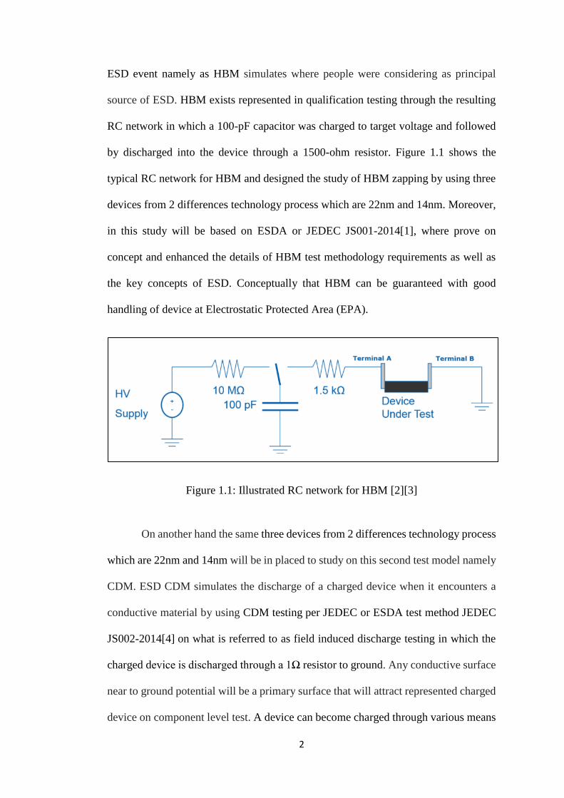
ESD event namely as HBM simulates where people were considering as principal
source of ESD. HBM exists represented in qualification testing through the resulting
RC network in which a 100-pF capacitor was charged to target voltage and followed
by discharged into the device through a 1500-ohm resistor. Figure 1.1 shows the
typical RC network for HBM and designed the study of HBM zapping by using three
devices from 2 differences technology process which are 22nm and 14nm. Moreover,
in this study will be based on ESDA or JEDEC JS001-2014[1], where prove on
concept and enhanced the details of HBM test methodology requirements as well as
the key concepts of ESD. Conceptually that HBM can be guaranteed with good
handling of device at Electrostatic Protected Area (EPA).
Figure 1.1: Illustrated RC network for HBM [2][3]
On another hand the same three devices from 2 differences technology process
which are 22nm and 14nm will be in placed to study on this second test model namely
CDM. ESD CDM simulates the discharge of a charged device when it encounters a
conductive material by using CDM testing per JEDEC or ESDA test method JEDEC
JS002-2014[4] on what is referred to as field induced discharge testing in which the
charged device is discharged through a 1Ω resistor to ground. Any conductive surface
near to ground potential will be a primary surface that will attract represented charged
device on component level test. A device can become charged through various means

3
including “triboelectrically”, by an electric field or inductively by a charged insulator.
Note the "charged" device abstains none net voltage on internal nodes of the device in
anticipation of the actual discharge, by which time high voltages are created as charge
flows from the device through the ground pin (pogo pin). Refer to below Figure 1.2
illustrated the effective capacitor network on the right and the field induced CDM
setup on the left.
Figure 1.2: CDM setup (left) and effective capacitor network (right) [2][4]
1.2 Importance and Challenges of Technology Scaling on
ESD
The main hidden rival in numerous semiconductor industrial factories is ESD
as it can damage components and devices damages that containing electronics. Thus,
ESD event adversely impact productivity, product quality and reliability where
directly caused a company’s reputation and profitability because of undetectable ESD
damage by quality control inspections. Throughout the advance technology process
scaling, ESD protection methodology and reliability challenges for the qualification

4
on 65nm and beyond have been accelerated the focuses on the ESD target levels starts
begin in HBM and CDM model in electronics industry [5].
Therefore, ESD robustness is much greater issue today with process scaling
leads the increased attention of customer satisfactions, cost reduction of ESD
protection, maximum yields and volume production. Just to ensure better product
reliability, it is critical that today’s design engineer understand the significant
differences among manufacturing environment and system end user environment ESD
testing.
A phenomenon reported, under ESD conditions the triggering voltage (Vt)
happens a drastic reduction of n-MOS and p-MOS for the scaled 90nm CMOS
technology devices in high performance applications. The merging of pockets
implants in a short gate length transistors the Vt will be reduce. Hence, this
phenomenon has a serious impact on design effective protection device due to the
placing restriction over the ESD sensitivity of output drivers. [6]
Three unlike characteristics of the technology trends will started impact the of
ESD sensitivity such as the input design protection difficulties with lower breakdown
voltages and thinner gate oxides, secondly followed by the ESD failure current value
lower due to the reduced drain junction breakdown voltages adequate output
protection. Nevertheless, the increased resistance and thinner metal interconnects for
ESD resistance connections elevated voltage pad near to relative lower ESD currents.
Semiconductor manufacturers and users are concerning on ESD testing
methodologies when comes to the current ever-changing and fast-paced business
environment, for example unpackaged die, shipped as unpackaged wafers, and
packaged silicon die. In ordered to put up this wide variety of different cases,
5
flexibility of ESD testing methodologies must be present. The existing of ESD
standards never disclosed the issue of facing the types and varieties of device being
shipped out by manufacturers. Thus, the works of shall be following respective ESD
JEDEC standards to correspond with universal guideline to establish mitigation plan
and rightful measures model in ESD control.
While in monitoring the leakage current before and after the ESD event
typically determined the ESD failure threshold. Generally, ESD damage is terms have
happened by having the leakage current shifted above certain predefined value usually
around 20-micron Ampere for smaller technology process (14nm) and 1 micron
Ampere on 22nm fabrication technology process. However, the shifted leakage current
for 22nm sometimes considered as shifted when more than 5x measured current value
post ESD event. This failure criterion is used in most of the automated ESD tester for
HBM or CDM.
JEDEC ESD Test Standard benefit guarantee consistency of ESD control
products and services and stability of ESD sensitive products that be responsible of
the comparison among competitive ESD control products and objective evaluation.
This JEDEC standard help diminish many of the conflicts between users and suppliers
when handling with ESD control products. The ESD Association responsible on
developed, implementation, auditing, qualification and certifying ESD control
programs in all the manufacturer test side to avoid confusion in marketplace.
The ESD test standard become harder to meet in event of the process
technology scaling drive due to none proper released standard that embedded overall
products types with descriptions on start and step test voltages. In fact, the standard
only defines the range of the classify products type thus the start voltage on ESD

6
sustaining levels will need to performed based on estimated specification stress level
on product where is compulsory to prove the ESD protection devices does not failed
at specification voltage stresses or in another word low voltage stresses. Margin
voltage stress are optional in any of the ESD test standard as it was to demonstrate the
effectiveness of ESD protection devices in testing standards for industrial level. Hence,
this is the potential gaps in JEDEC test standard in industrial practice. Any misconduct
of the test setup leads to in accurate of ESD stress results. Therefore, in this research
one of intend also to improve on the standard guideline for ESD test house vendor
based on the suggested methodology in Chapter 3.
1.3 Problem Statement
ESD become greater focus during stress condition for quality control
conformance and reliability in any of the product qualification and semiconductor
business process by mimic the potential ESD design violation, effectiveness of final
test setup and or early prevention on ESD event. Technologies endure to shrink and
circuit speed anxieties continue to increase creating CDM as one of component level
ESD facing difficulty to meet the current CDM levels. In recent proven damage
signature by ESD, CDM become unique and important test method for IC component
ESD testing due to fast ESD discharges with high peak current cannot be reproduced
by HBM. Existing JEDEC standard also does not release the proper voltage stress
level on CDM and HBM nonetheless only the voltage range by products classification.
However, in real life cases, ESD stress qualification usually do not always
static or unchanged as per predictable JEDEC target level. Moreover, there are a lot
more factors that impact the ESD model for example pins count, die size and leakage
7
measurement of device and none efficient ESD protection design due to the
technology scaling. Hence, HBM and CDM stress level for System-on-chip (SOC)
estimation and prediction on 14nm and 22nm would be added topic.
1.4 Research Objective
The aim is to optimize and improve the ESD methodology regarding JEDEC
standard in pin grouping allocation to avoid over zapping induced as well as tested at
Automatic Test Equipment (ATE) or final functional test on the leakage degradation
post zapping to measure the products functionality. The objectives of this thesis are as
follows:
i. To analyze CDM and HBM stress level and margin stress level based
on actual SOC devices on 14nm and 22nm respectively across Product
A, Product B and Product C ensure meeting ESD criteria with JEDEC
Industrial Council Standard and propose the new guideline for
improvement on HBM testing methodology for industrial vendor
during preliminary pin grouping step to avoid violation in JEDEC
standard. Also, using peak current (Ipeak) method to determine CDM
stress voltage and indirect defect localization method by having ESD
stress determine early failure detection for ESD failure.
ii. To analyze actual obtained result by using leakage current
measurement increases for three products with different fabrication
process technology products by using Jump Statistic Software (JMP)
post ESD stress to define failed ESD stress level.

8
1.5 Research Scopes
The thesis covers research by using 22nm on Product A and 14nm on Product
B and Product C. Current market trend was focus on 22nm and 14nm technologies
where both technologies are stable during fabrication process. Thus, research scope
focus on specified ESD model consisted of HBM and CDM from 22nm and 14nm
considering similar market segments. Main reason in this research using Product A
(22nm) and Product C (14nm) from phone device segments is to understand the impact
of fabrication technologies. While Product B application usage is network connection
device because this is 14nm due to different product segment that can be used as
baseline reference. Then, the measurement current leakage was analyzed by using JMP
statistical software tool.
1.6 Thesis Outline
Chapter 1 introduces the background of ESD study in the very beginning. Then,
it highlights the problems in estimation of HBM and CDM stress level in SOC and
importance of ESD in semiconductor industry. Lastly, problem statement and research
objective of this study is outlined. Chapter 2 provides the literature review. Chapter 3
presents the methodology to design of experiment between 22nm and 14nm process
technology on CDM and HBM. Chapter 4 presents the results outlined in the
methodology presented in Chapter 3. Chapter 5 draws the conclusion of this study and
presents the future works that can be extended to further improve the scope and depth
of this study.

9
LITERATURE REVIEW
2.0 Chapter Overview
This chapter reviews the overview of ESD test, standard and method in
semiconductor industry. Section 2.1 explains on the basic of component level ESD
model such as HBM and CDM and comparing its differences as well as including
introduces the tester for ESD test. Section 2.2 introduces the ESD testing method and
in view of JEDEC Industrial Council Standards and fundamental requirements for
both HBM and CDM including the Failure Criteria. Section 2.3 explains on the impact
of technology scaling of ESD in more details and effect to measurement leakage
current characteristics based on 14nm and 22nm process technology devices. Section
2.4 reviews what is JMP Statistic Tools and its purpose of usage for analyzing before
and after ESD test.
2.1 Basic of Electrostatic Discharge Testing Model
Electrostatic Discharge (ESD) is the spontaneous and momentary electric
current that flows between two objects at different electrical potentials [7]. This
imbalance of charges usually able to drift the static charge to higher electrostatic field
where the charge flow potential induces a spark or minor electric shock just like many
people do experience when walking across a carpeted floor and touched electronic
device or metal doorknob [3]. ESD become very crucial in semiconductor industrial

10
because the device electrical characteristic will be affected, device get degraded with
increases of the leakage current measurement after ESD event or the worst scenario
which the device destroyed and equipment malfunction. Moreover, voguish increasing
attention commencing the ESD effects commonly impact the performance of
semiconductor integrated circuits towards product quality and production yield.
Technology scaling has also impacted the silicon area, amalgamated with advanced
package technology the high-speed circuit performance and smaller device sizes
causing current level of ESD design in delay and eventually a problem for ESD stress.
Besides, the ESD robustness several factors such as the cost reduction, customer
satisfaction, high yield and volume production, a more realistic target level on meeting
the ESD voltage stress level and step voltages by means of its IC performance
constraints are also increased [8]. Thus, ESD robustness as a function of technology
scaling is continuing to decrease while circuit speed demands kept increasing, forcing
changes in the technology strategies and roadmaps [9]. However, in semiconductors
device manufacturer ESD test still a major consideration to get the product quality and
more reliable products. ESD importance drive concerned inherited ESD Associations
namely JEDEC standards established where leads numerous testing standards releases
to addressing several of technical doubt and requirements in industrial segment. Many
of the ESD test model in industrial yet the most popular in IC industrial are Human
Body Model (HBM) and Charged Device Model (CDM).

11
2.1.1 Human Body Charge (HBM)
Human Body Model (HBM) is one of the common testing ESD sensitivity
qualification. HBM model is designed to simulate the direct transmission for
electrostatic charge from human body to a device which also known as component
level ESD test as illustrated in Figure 2.1. The model represented has a target charged
voltage with a 100-pF capacitor and a 1.5 KΩ resistor to discharge the device and
switch into device under test (DUT) [10]. The equivalent circuit for HBM was shown
in earlier Section 1.1 as represent in Figure 1.1. Gate oxides damage, metal layer
melted, metal penetration and spike on contact are the common failure modes for
HBM test. Table 2.1 shown typical example on charge generated scenarios and its
results of voltage levels [10].
Figure 2.1: Human body cause by electric discharge on a DUT and HBM Equivalent
circuit [10]
12
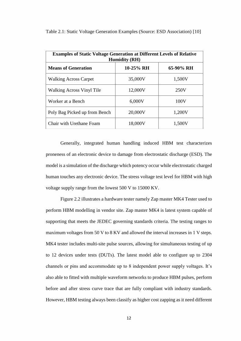
Table 2.1: Static Voltage Generation Examples (Source: ESD Association) [10]
Generally, integrated human handling induced HBM test characterizes
proneness of an electronic device to damage from electrostatic discharge (ESD). The
model is a simulation of the discharge which potency occur while electrostatic charged
human touches any electronic device. The stress voltage test level for HBM with high
voltage supply range from the lowest 500 V to 15000 KV.
Figure 2.2 illustrates a hardware tester namely Zap master MK4 Tester used to
perform HBM modelling in vendor site. Zap master MK4 is latest system capable of
supporting that meets the JEDEC governing standards criteria. The testing ranges to
maximum voltages from 50 V to 8 KV and allowed the interval increases in 1 V steps.
MK4 tester includes multi-site pulse sources, allowing for simultaneous testing of up
to 12 devices under tests (DUTs). The latest model able to configure up to 2304
channels or pins and accommodate up to 8 independent power supply voltages. It’s
also able to fitted with multiple waveform networks to produce HBM pulses, perform
before and after stress curve trace that are fully compliant with industry standards.
However, HBM testing always been classify as higher cost zapping as it need different
Examples of Static Voltage Generation at Different Levels of Relative
Humidity (RH)
Means of Generation 10-25% RH 65-90% RH
Walking Across Carpet 35,000V 1,500V
Walking Across Vinyl Tile 12,000V 250V
Worker at a Bench 6,000V 100V
Poly Bag Picked up from Bench 20,000V 1,200V
Chair with Urethane Foam 18,000V 1,500V

13
custom made standard sockets that need to accommodate a wide range of normal
package types.
Figure 2.2: MK4 Tester for HBM Stress Test [10]
MK4 system tester curve trace shown in Figure 2.3 with the ± 10% tolerance setup
from reference point in comparing with initial or normal IV curve before ESD test.
The reference point is the range for the IV curve to shift after ESD, any IV curve more
than ± 10% consider failed IV curve on that pin. In any condition the IV curve does
not shift more than the tolerance range of ± 10% then this pin only considers as shifted
IV curve and need to determine the device pass or fail with Automatic Test Equipment
(ATE) as per failing criteria standard.
ATE is any apparatus that performs tests on a device, known as the DUT,
equipment under test or unit under test using automation to quickly perform
measurements and evaluate the test results. An ATE can be a simple computer-
controlled digital multimeter, or a complicated system containing dozens of complex

14
test instruments real or simulated electronic test equipment capable of automatically
testing and diagnosing faults in sophisticated electronic packaged parts or on wafer
testing, including system on chips and integrated circuits.
ATE is widely used in the electronic manufacturing industry to test electronic
components and systems after being fabricated. ATE is also used to test avionics and
the electronic modules in automobiles. It is used in military applications like radar and
wireless communication. Semiconductor ATE, named for testing semiconductor
devices, can test a wide range of electronic devices and systems, from simple
components such as resistors, capacitors, and inductors to integrated circuits, printed
circuit boards, and complex, completely assembled electronic systems. ATE systems
are designed to reduce the amount of test time needed to verify that a device works or
to quickly find its faults before the part has a chance to be used in a final consumer
product. To reduce manufacturing costs and improve yield, semiconductor devices
should be tested after being fabricated to prevent defective devices ending up with the
consumer. Not all devices are tested equally. Testing adds costs, so low-cost
components are rarely tested completely, whereas medical or high costs components
where reliability is important are frequently tested.
However, testing the device for all parameters may or may not be required
depending on the device functionality and end user. For example, if the device finds
application in medical or life-saving products then many of its parameters must be
tested, and some of the parameters must be guaranteed. But deciding on the parameters
to be tested is a complex decision based on cost vs yield. If the device is a complex
digital device, with thousands of gates, then test fault coverage should be calculated.
Here again, the decision is complex based on test economics, based on frequency,
number and type of IOs in the device and the end-use application.

15
Figure 2.3 Example of initial IV cure trace with ± 10% reference point [10]
2.1.2 Charged Device Model (CDM)
Charged Device Model (CDM) is component level ESD stress used to
simulates the rapid discharge of a charged device when it encounters a conductive
material. Simulating production processes and manufacturing environment such as
machine handler where charges in machine usually remain on indefinitely induced
electrical charge overtime on devices is CDM testing procedure [10]. In a way,
CDM also measures the effectiveness on how fast the protective device responds
to high voltage. One of the example CDM simulation is important during the
backend device packing, during packing the metal surface get hit when the device
slide down from shipping tube. Besides, the capacitance discharge that built up by
the residual, the device encounter a grounded conductor DUT is charged to zap
voltage with one pin is grounded. Figure 2.4 shown the CDM mechanism on a DUT

16
[10]. The DUT placed on its back facing upward on a testing board for CDM test.
In field-induced method, the DUT’s potential is raised by applying the stress
voltage for example 500 V to the field charging electrode or charge plate which
creates an electric field to charge up the DUT. Once the DUT is charged up, the
pogo probe for instance discharge probe is placed over the pin under test and
encounters it, thereby discharging the charges from the DUT to the ground.
Figure 2.4 Show the CDM mechanism on a DUT [10]
Figure 2.5 illustrates a hardware tester namely Orion2 tester by Fisher
Scientific used to perform CDM modelling in most of semiconductor industrial
ESD test vendor site. Orion2 with feature of capturing real discharge waveform,
each pin can be tested multiple times based on the requested requirement at
different stress voltage.

17
However, based on previous research cumulative zapping on the devices
will induce latent failure and the ESD result does not accurate to the real stress
voltage level. CDM ESD testing with Orion 2 tester generated more accurate result
and time consume faster than any other tester. It’s also manage to maintain the
relative humidity and test environment for CDM testing to ensure consistency by
providing the function of repeatable results for certain un-socket test occurred in
any event.
CDM only allowed one DUT tested in a time with no custom fixture board
required and able to support different packages sizes however larger package size
may be constrained. CDM discharged waveform required to review with the
oscilloscope technology at 6 GHz. The before and after tester calibration
commonly in JEDEC standard to be completed with small and large disc to ensure
the results accuracy.
Figure 2.5: Orion2 Tester for CDM Stress Test [10]

18
2.1.3 HBM and CDM Failure Criteria
From the ESD standard the devices are determine as a failure only if it fails at
ATE where all the parameter in datasheet shall be tested. For HBM, unpowered IV
curve trace is recommended before and after ESD. Unpowered curve trace was done
with a requirement by grounded all power and ground rails to reduce the false IV curve
trace failed. However, IV curve trace is not enough to make the final decision for the
ESD failure as mentioned earlier ATE will be the primary criterion. Besides, curve
trace is used as part of method to identify the possible weak pins guide in decisive the
ESD withstand voltage. The curve trace reference point should be adjusted to 4% to
verify the repeatability of the pins with tester and build sufficient confident level,
however the initial value to envelope the current shift is at 10%. The curve trace data
benefit at the early stage of new product which functional testing in the leakage test
pins lack of the screening capability. Despite, the curve trace result also able to
determine the shifted leakage pin and changes on the pin performance [4][1]. After
ATE testing, a leakage current increases and used to monitor the latent damaged where
decision will be depended on reliability engineer to decide the leakage current increase
enough to consider fail after ESD.
2.2 ESD JEDEC Test Standard
The HBM and CDM risk assessment evaluation from JEDEC standard are used
for reference to provide a standard procedure such as test methods, pin classification
method, waveform verification, IV curve trace criteria, lowest passing level criteria
for all devices classification, failure criteria and many more.
19
2.2.1 HBM JEDEC Standard
Current revision of the JEDEC JS-001-2014 test standard for HBM test merely
define the start voltage and the sustained or withstand voltage level does not
specifically listed out for different technology process device. For instance, in this
research the aim to determine the withstand voltage for 22nm technology process
device which is Product A and 14nm technology device for Product B and Product C.
Like all the devices in industrial the JEDEC standard classification only providing a
range of the voltage start stress range. Moreover, the step test voltage also does not
specify leading many standards to the step range and the margin test for the devices
barely continue to stress until the withstand stress voltage or a significant measurement
leakage shifted. [4]
In this section, several important JEDEC standard components will be review
for example HBM stress tester qualification and waveform verification for the
accuracy, pin grouping and combinations criteria and HBM sensitivity classification
table. Pin grouping and combination table are crucial to determine the pin grouping
before HBM test however several criteria does not capture accurately in the standard.
The standard clarification needed to bring to the industrial represent.
Qualification for HBM tester and fixed shall be done periodically to ensure the
functionality of the tester does not degraded. This shall be done by ensure the Human
Body Model Simulator meeting the equipment standard. Figure 2.6 illustrated parasitic
capacitance and inductance influenced the tester performance. Thus, the calibration
for the waveform need to performed to ensure the HBM pulse required meets the
standard. The two reference pin pairs to the ESD stress socket consist of longest wire
path to pulse generation circuit namely Terminal A while Terminal B is the shortest
wire path to pulse where this info typically embedded in the test fixture board manual.

20
Measuring Terminal B waveform, the current probe placed to short wire between pins.
Clamp positive sockets by insert the shorting wire between the socket pins connected
to Terminals A and B and hold in place by closing the clamp meanwhile shorting wire
between the socket pins connected to Terminals A and B for non-positive clamp
sockets. When placing the current probe between resistor and Terminal B, the 500
ohm pins measured. Thus, the calibration for the waveform need to performed to
ensure the HBM pulse required meets the standard. The process of determine
acceptability of the equipment for consisted several procedures such as measurement
pin pairs producer well pursued, capturing the current probe waveform for the usage
to determine the parameter value on wave specification in Table 2.2. This is crucial
before the HBM test started [4].
In this section, several important JEDEC standard components will be review
for example waveform specification, pin grouping and combinations criteria, ESD
sensitivity classification table and show some of the IV curve trace before and after
ESD on valid fail pins.
Figure 2.6: Simplified HBM Simulator Load [4]
21
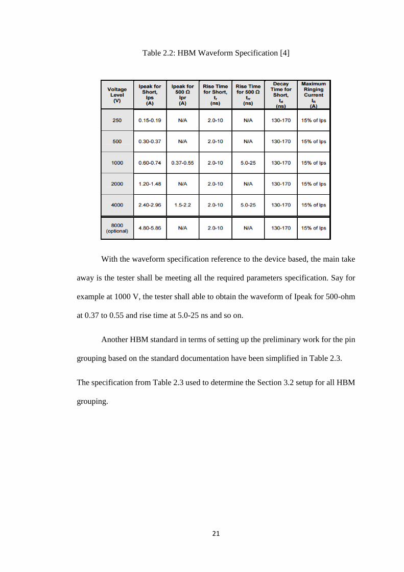
Table 2.2: HBM Waveform Specification [4]
With the waveform specification reference to the device based, the main take
away is the tester shall be meeting all the required parameters specification. Say for
example at 1000 V, the tester shall able to obtain the waveform of Ipeak for 500-ohm
at 0.37 to 0.55 and rise time at 5.0-25 ns and so on.
Another HBM standard in terms of setting up the preliminary work for the pin
grouping based on the standard documentation have been simplified in Table 2.3.
The specification from Table 2.3 used to determine the Section 3.2 setup for all HBM
grouping.

22
Table 2.3: Pin Combination Sets for Integrated Circuits [4]
Upon ESD stress completed, IV curve will be obtaining and the device is
measured to check if the device has failed. The highest voltage level that the device
can survive is called “ESD withstand voltage (Vw)”, which can be used to classify the
ESD sensitivity of the device. The ESD sensitivity classification for a device tested by
HBM is shown in Table 2.4, which gives an indication of the level of ESD protection
required. The table below decode as if a device HBM goal with 1000 V it should
classify as Class 1C.

23
Table 2.4: JEDEC HBM Sensitivity Classification [4]
Class ESD withstand voltage, Vw
0 0 ~ 250 V
1A 250 ~ 500 V
1B 500 ~ 1000 V
1C 1000 ~ 2000 V
2 2000 ~ 4000 V
3A 4000 ~ 8000 V
3B > 8000 V
2.2.2 CDM JEDEC Standard
Latest, JEDEC for CDM is JEDEC JS-002-2014 test standard for CDM where
the purpose of this standard is to refine the classifying devices, standard test procedure
and known microcircuits according CDM sensitivity to field induce charge on damage
or degradation exposure. For instance, in this research the aim to determine the
withstand voltage for 22nm technology process device which is Product A and 14nm
technology device for Product B and Product C. Like all the devices in industrial the
JEDEC standard classification only providing a range of the voltage start stress range.
As far as the research, from previous technical paper the withstand voltage for CDM
were not recorded in specifically but there is some study on wide range of process
technology which will also review in next Section 2.3 on the technology scaling on
ESD. The step test voltage also does not specify leading many standards to the step
range and the margin test for the devices barely continue to stress until the withstand
24
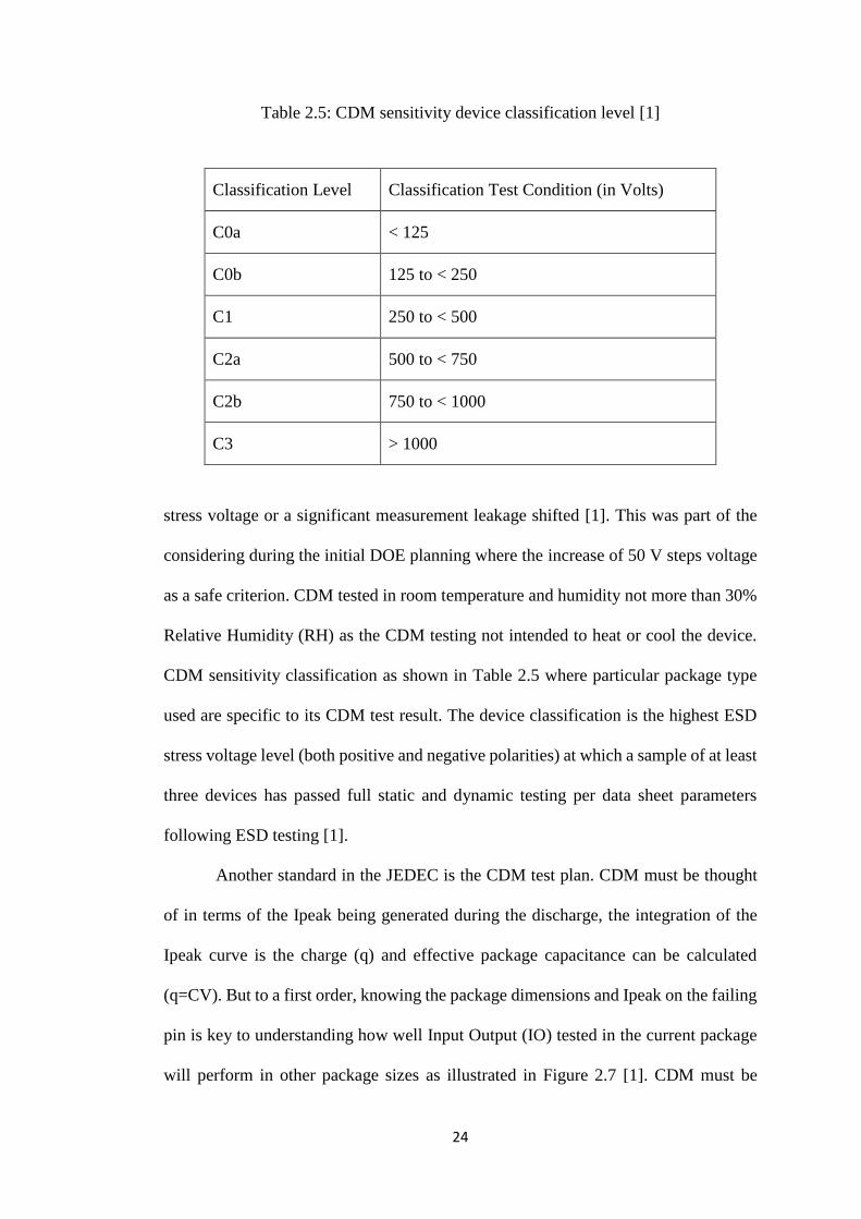
Table 2.5: CDM sensitivity device classification level [1]
Classification Level Classification Test Condition (in Volts)
C0a < 125
C0b 125 to < 250
C1 250 to < 500
C2a 500 to < 750
C2b 750 to < 1000
C3 > 1000
stress voltage or a significant measurement leakage shifted [1]. This was part of the
considering during the initial DOE planning where the increase of 50 V steps voltage
as a safe criterion. CDM tested in room temperature and humidity not more than 30%
Relative Humidity (RH) as the CDM testing not intended to heat or cool the device.
CDM sensitivity classification as shown in Table 2.5 where particular package type
used are specific to its CDM test result. The device classification is the highest ESD
stress voltage level (both positive and negative polarities) at which a sample of at least
three devices has passed full static and dynamic testing per data sheet parameters
following ESD testing [1].
Another standard in the JEDEC is the CDM test plan. CDM must be thought
of in terms of the Ipeak being generated during the discharge, the integration of the
Ipeak curve is the charge (q) and effective package capacitance can be calculated
(q=CV). But to a first order, knowing the package dimensions and Ipeak on the failing
pin is key to understanding how well Input Output (IO) tested in the current package
will perform in other package sizes as illustrated in Figure 2.7 [1]. CDM must be