Embed Size (px)
Citation preview
IEEE TRANSACTIONS ON VERY LARGE SCALE INTEGRATION (VLSI) SYSTEMS, VOL. 29, NO. 6, JUNE 2021 1061
EM Side-Channel Countermeasure forSwitched-Capacitor DC–DC Converters
Based on Amplitude ModulationRuzica Jevtic , Senior Member, IEEE, Marko Ylitolva, Member, IEEE, Clara Calonge,
Martti Ojanen, Tero Santti, Member, IEEE, and Lauri Koskinen, Member, IEEE
Abstract— The security of IoT devices is becoming a majorconcern in industry. Noninvasive side-channel attacks pose aserious threat as they are capable of extracting secret informationfrom distance while using low-cost equipment. In this article,we propose an efficient countermeasure technique against theelectromagnetic (EM) side-channel attacks. The technique isapplied to switched-capacitor (SC) dc–dc converters and is basedon amplitude modulation of the load signal by the convertercapacitance that acts as a carrier. We verify the proposedtechnique by using a reliable evaluation metric that predictsthe correlation between the encryption secret key and theattacker’s measured signal. The results show that the proposedtechnique can achieve cross correlation coefficients as low as 0.2,disabling the attacker from extracting the sensitive information.In addition, test vector leakage assessment (TVLA) ρ-test indi-cates that the number of leaky points for advanced encryptionstandard (AES) execution drops from 62 for unprotected circuitto zero for the circuit secured by the proposed technique. TVLAt-statistic is decreased by three orders of magnitude in theprotected AES execution.
Index Terms— Amplitude modulation (AM), security,side-channel attacks, switched-capacitor (SC) dc–dc converters.
I. INTRODUCTION
NEW security threats are emerging as a consequence ofthe ever-increasing number of devices connected to the
Internet. Each device acts as a network node in the Internet-of-Things (IoT) and needs to be available around the clock toprovide information and control signals to the environment.While it is impossible to predict the exact consequences ofthe massive breakthrough of the IoT network, two key factors
Manuscript received September 3, 2020; revised November 24, 2020 andMarch 2, 2021; accepted March 27, 2021. Date of publication April 16,2021; date of current version June 4, 2021. This research was fundedby the Ministry of Science, Innovation and Universities of Spain, andthe European Regional Development Fund of the European Commission,Grant No. RTI2018-095324-B-I00 and by the FitOptiVis Project funded bythe ECSEL Joint Undertaking under Grant H2020-ECSEL-2017-2-783162.(Corresponding author: Ruzica Jevtic.)
Ruzica Jevtic and Clara Calonge are with Escuela Politecnica Superior,Universidad San Pablo-CEU, 28003 Madrid, Spain (e-mail:[email protected]; [email protected]).
Marko Ylitolva is with the Department of Future Technologies, Universityof Turku, 20500 Turku, Finland, and also with CoreHW, 20100 Turku, Finland(e-mail: [email protected]).
Martti Ojanen, Tero Santti, and Lauri Koskinen are with the Departmentof Future Technologies, University of Turku, 20500 Turku, Finland (e-mail:[email protected]; [email protected]; [email protected]).
Color versions of one or more figures in this article are available athttps://doi.org/10.1109/TVLSI.2021.3070687.
Digital Object Identifier 10.1109/TVLSI.2021.3070687
are evident: IoT nodes need to be energy-efficient and secureagainst hacking.
While there are a multitude of methods to hack devices,side-channel attacks can be the most cunning since con-ventional cryptographic methods, the basis of most secu-rity measures, inherently leak side-channel information. Mostside-channel attacks are somewhat invasive and require accessto the device. For example, power attacks usually require asmall resistor to be inserted in the ground line of the device.By measuring the voltage over the resistance, the attacker canget the information on the current. The current depends on thedata that are being processed and can indirectly provide theconfidential information on the secret key.
Noninvasive side-channel attacks pose a serious threat tothe security of cryptographic devices. The attacks cannot bedetected and usually require only a simple low-cost equipment.This type of attacks relies on measuring electromagnetic (EM)radiation of the chip.
Recent studies show that the EM emanations differ fromand provide more information than the leakage from otherconventional side channels, such as timing and power[1]–[5]. EM attacks are based on the measurement of EMwaves that are radiated from the device. Electrical and mag-netic fields depend on the derivative of the voltage and current,so the leaked signal is fundamentally different from the leakedsignal in power attacks. While power attacks rely on theabsolute current value and the time moments that indicatewhen the current changes its value, the EM attacks dependon the current and voltage slope. In addition, EM attacks arecompletely contactless since it is not necessary to tamper withthe device, and they can provide more information in spatial,temporal, and frequency domains [4], [5].
In this work, we focus on the EM leakage from the powersupply signal since this is the strongest signal in the chipand thus, most easily attacked [3]. Power distribution networkconsists of voltage regulators that need to adapt the batteryvoltage to the power supply of the chip. The regulators arealso used for dynamic voltage scaling to improve the energyefficiency of the IoT devices [6]–[8].
Inductive converters are efficient but have bulky inductivecomponents off chip that increase the size of the chip andare therefore not suitable for small IoT nodes. Recent workhas reported security techniques for fully integrated buckconverters [9]. However, the wirebond inductances used in
1063-8210 © 2021 IEEE. Personal use is permitted, but republication/redistribution requires IEEE permission.See https://www.ieee.org/publications/rights/index.html for more information.
Authorized licensed use limited to: Univ Politecnica de Madrid. Downloaded on July 23,2021 at 10:44:15 UTC from IEEE Xplore. Restrictions apply.
1062 IEEE TRANSACTIONS ON VERY LARGE SCALE INTEGRATION (VLSI) SYSTEMS, VOL. 29, NO. 6, JUNE 2021
the converter can still leak critical information in form of EMemanations. The inductances act as a transmitting antenna dueto the ac current that passes through them. They radiate EMwaves that contain information on the switching frequencyand duty cycle of the converter, both highly dependent onthe load.
Linear regulators are implemented on-chip, but they areincapable of achieving high efficiency across a wide rangeof output voltages. Work in [10] reports improvement inside-channel resistance against power attacks, at the costof deteriorating dynamic loop response, while work in [11]changes the reference voltage randomly in order to addadditional noise to the leaked current signal.
In this work, we consider single-phase switched-capacitor(SC) voltage regulators, which can be fully integrated on-chip, do not have bulky inductive elements, and can bereconfigured to achieve multiple-output voltage levels withouta significant loss in efficiency [6], [12]. They also haveseveral tuning knobs to randomize the output voltage anddecorrelate the chip activity from the physical leakages of thechip.
Several countermeasures against side-channel attacksapplied to SC dc–dc converters have been reported in theliterature [13]–[19]. However, they are either time-consumingas they optimize the design at the gate and/or layout level[17]–[19] or they are employed as protection from differentialpower attacks, rather than EM attacks [13]–[16]. In addition,most of the published techniques do not explore the causalityof the leaked signal, as the work proposed here.
This work analyzes in detail the physical nature of theleaked EM signal. We prove that the signal obtained fromcapacitance values in time acts as a carrier in the amplitudemodulation (AM) of the load signal. The resulting AM signalis leaked to the outside world in form of EM emanations.Based on this analysis, we propose to change the availablecapacitance in the converter in a deterministic manner duringeach conversion period. We change the capacitance value tocreate overlap in the load frequency spectrum, hence disablingthe attacker from recovering the original load signal.
While the work in [16] is also based on the functionalityof the switched-capacitor dc–dc converter, it focuses on theprotection from the power attacks and masks the residualvoltage on the capacitances from the power measured at theinput. However, it is still likely that EM probe is able todetect the activity of the capacitances that are not connectedto the input and reveal information on the load. In this work,we assume that the attacker has a complete information on thevoltage over the flying capacitor via EM probe and proposea methodology that offers protection from EM side-channelattacks.
This article is organized as follows. Section II gives anoverview on the implementation and functionality of the SCdc–dc converter. Section III describes the analysis of the leakedEM signal. In Section IV, the proposed security techniqueis described in detail. In Section V, we present the experi-mental results. Section VI studies the impact of the proposedtechnique on the power and area. Section VII concludes thisarticle.
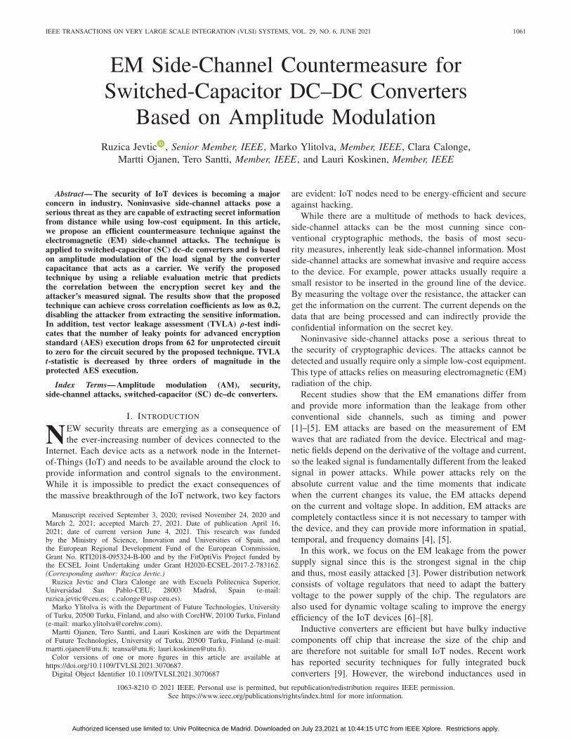
Fig. 1. Single-phase SC dc–dc converter operation: schematic with equivalentwaveforms.
II. SC DC–DC CONVERTER SPECIFICATIONS
Dynamic voltage scrambling is one of the side-channelcountermeasures that randomly changes power supply volt-age level in order to decorrelate the leaked signal fromthe processed data [13]–[16], [22]–[24]. This technique haslow area and power overhead and has proved to be veryeffective against power attacks when applied to multiphaseswitched-capacitor dc–dc converters.
Since we consider single-phase switched-capacitor dc–dcconverters, we adapt dynamic voltage scrambling to this typeof converters by changing the value of the flying capacitorrandomly. From here on, we call this technique random powerscramble (RPS) technique.
In order to study the exact effects of this technique againstEM attacks when applied to single-phase SC dc–dc converters,we start by examining the operation of the 2:1 step downconverter shown in Fig. 1 [12]. The converter operates in twononoverlapping phases φ1 and φ2. In phase φ1, SW1 andSW4 are turned on, and SW2 and SW3 are turned off, so theflying capacitor is connected between the input voltage and theoutput, and the capacitor is charging. In the second phase, φ2,SW2, and SW3 are turned on, and SW1 and SW4 are turnedoff, so the flying capacitor is connected between the outputand the ground and is discharging. The equivalent waveformson the capacitor and at the output are given in the same figure.
The ripple that appears at the output is usually suppressedby using a very large decoupling capacitance or interleavingthe phases of the converter. In this work, we consider thatthe output voltage ripple specifications of the dc–dc converterare not so strict, as this have proved to increase the energysavings of the systems considerably [6], [8], [21]. Largevoltage ripple would normally cause functional errors, butthe adaptive error-protection technology presented in [8] canwithstand this ripple. Also, the voltage ripple adds an elementof entropy to the system both in the time and voltage domains.Two executions of the same load may differ in power andtotal execution time, depending on whether the supply voltagewas mostly at the high or low end of the ripple during theexecution. This entropy serves as additional security againstside-channel attacks.
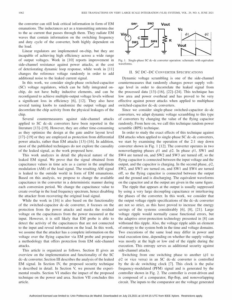
Switching from one switching phase to another (φ1 toφ2 or vice versa) in an SC dc–dc converter is controlledby the dc–dc switching clock [7]. This clock is the pulsefrequency-modulated (PFM) signal and is generated by thecontroller shown in Fig. 2. The controller is event-driven andis composed of a comparator, flip-flop, and nonoverlappingcircuit. The inputs to the comparator are the voltage generated
Authorized licensed use limited to: Univ Politecnica de Madrid. Downloaded on July 23,2021 at 10:44:15 UTC from IEEE Xplore. Restrictions apply.
JEVTIC et al.: EM SIDE-CHANNEL COUNTERMEASURE FOR SWITCHED-CAPACITOR DC–DC CONVERTERS 1063
Fig. 2. Single-phase SC dc–dc converter control logic.
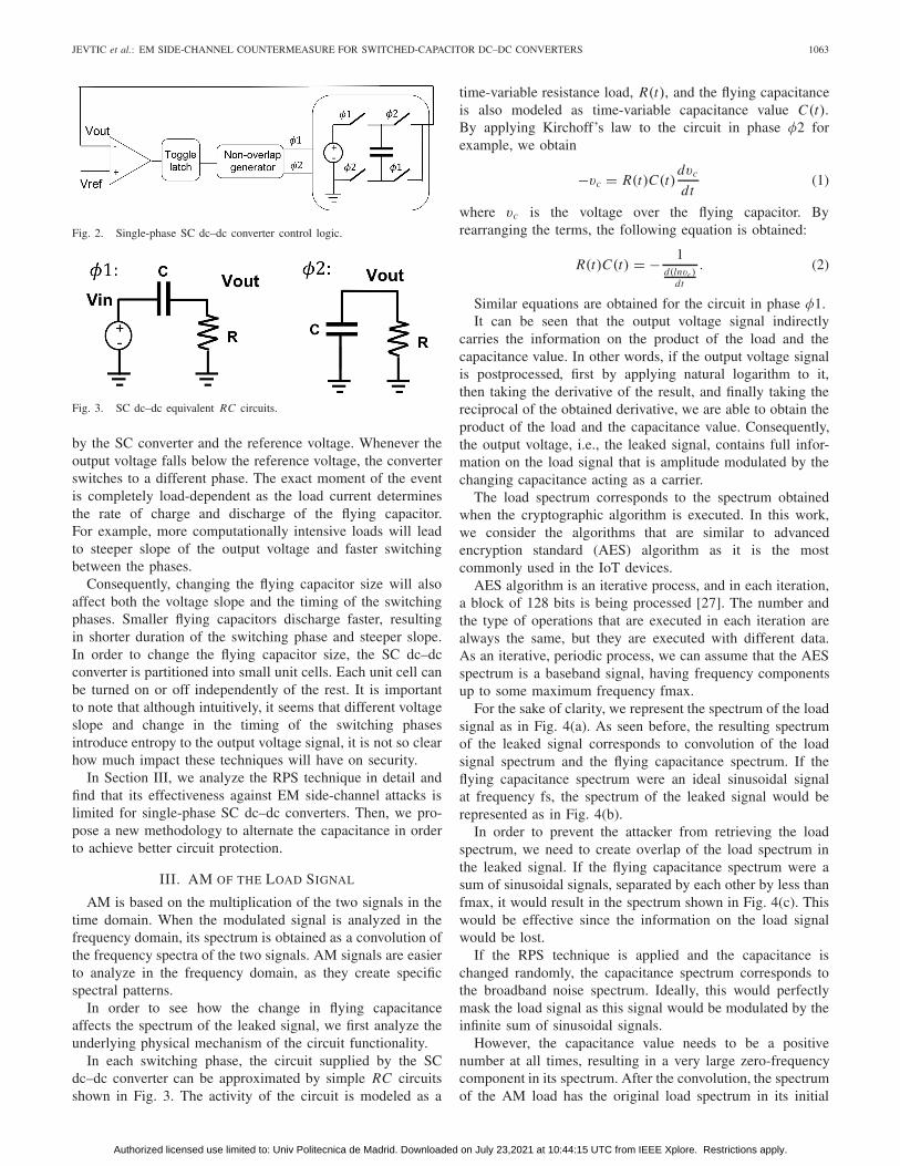
Fig. 3. SC dc–dc equivalent RC circuits.
by the SC converter and the reference voltage. Whenever theoutput voltage falls below the reference voltage, the converterswitches to a different phase. The exact moment of the eventis completely load-dependent as the load current determinesthe rate of charge and discharge of the flying capacitor.For example, more computationally intensive loads will leadto steeper slope of the output voltage and faster switchingbetween the phases.
Consequently, changing the flying capacitor size will alsoaffect both the voltage slope and the timing of the switchingphases. Smaller flying capacitors discharge faster, resultingin shorter duration of the switching phase and steeper slope.In order to change the flying capacitor size, the SC dc–dcconverter is partitioned into small unit cells. Each unit cell canbe turned on or off independently of the rest. It is importantto note that although intuitively, it seems that different voltageslope and change in the timing of the switching phasesintroduce entropy to the output voltage signal, it is not so clearhow much impact these techniques will have on security.
In Section III, we analyze the RPS technique in detail andfind that its effectiveness against EM side-channel attacks islimited for single-phase SC dc–dc converters. Then, we pro-pose a new methodology to alternate the capacitance in orderto achieve better circuit protection.
III. AM OF THE LOAD SIGNAL
AM is based on the multiplication of the two signals in thetime domain. When the modulated signal is analyzed in thefrequency domain, its spectrum is obtained as a convolution ofthe frequency spectra of the two signals. AM signals are easierto analyze in the frequency domain, as they create specificspectral patterns.
In order to see how the change in flying capacitanceaffects the spectrum of the leaked signal, we first analyze theunderlying physical mechanism of the circuit functionality.
In each switching phase, the circuit supplied by the SCdc–dc converter can be approximated by simple RC circuitsshown in Fig. 3. The activity of the circuit is modeled as a
time-variable resistance load, R(t), and the flying capacitanceis also modeled as time-variable capacitance value C(t).By applying Kirchoff’s law to the circuit in phase φ2 forexample, we obtain
−vc = R(t)C(t)dvc
dt(1)
where vc is the voltage over the flying capacitor. Byrearranging the terms, the following equation is obtained:
R(t)C(t) = − 1d(lnvc)
dt
. (2)
Similar equations are obtained for the circuit in phase φ1.It can be seen that the output voltage signal indirectly
carries the information on the product of the load and thecapacitance value. In other words, if the output voltage signalis postprocessed, first by applying natural logarithm to it,then taking the derivative of the result, and finally taking thereciprocal of the obtained derivative, we are able to obtain theproduct of the load and the capacitance value. Consequently,the output voltage, i.e., the leaked signal, contains full infor-mation on the load signal that is amplitude modulated by thechanging capacitance acting as a carrier.
The load spectrum corresponds to the spectrum obtainedwhen the cryptographic algorithm is executed. In this work,we consider the algorithms that are similar to advancedencryption standard (AES) algorithm as it is the mostcommonly used in the IoT devices.
AES algorithm is an iterative process, and in each iteration,a block of 128 bits is being processed [27]. The number andthe type of operations that are executed in each iteration arealways the same, but they are executed with different data.As an iterative, periodic process, we can assume that the AESspectrum is a baseband signal, having frequency componentsup to some maximum frequency fmax.
For the sake of clarity, we represent the spectrum of the loadsignal as in Fig. 4(a). As seen before, the resulting spectrumof the leaked signal corresponds to convolution of the loadsignal spectrum and the flying capacitance spectrum. If theflying capacitance spectrum were an ideal sinusoidal signalat frequency fs, the spectrum of the leaked signal would berepresented as in Fig. 4(b).
In order to prevent the attacker from retrieving the loadspectrum, we need to create overlap of the load spectrum inthe leaked signal. If the flying capacitance spectrum were asum of sinusoidal signals, separated by each other by less thanfmax, it would result in the spectrum shown in Fig. 4(c). Thiswould be effective since the information on the load signalwould be lost.
If the RPS technique is applied and the capacitance ischanged randomly, the capacitance spectrum corresponds tothe broadband noise spectrum. Ideally, this would perfectlymask the load signal as this signal would be modulated by theinfinite sum of sinusoidal signals.
However, the capacitance value needs to be a positivenumber at all times, resulting in a very large zero-frequencycomponent in its spectrum. After the convolution, the spectrumof the AM load has the original load spectrum in its initial
Authorized licensed use limited to: Univ Politecnica de Madrid. Downloaded on July 23,2021 at 10:44:15 UTC from IEEE Xplore. Restrictions apply.
1064 IEEE TRANSACTIONS ON VERY LARGE SCALE INTEGRATION (VLSI) SYSTEMS, VOL. 29, NO. 6, JUNE 2021
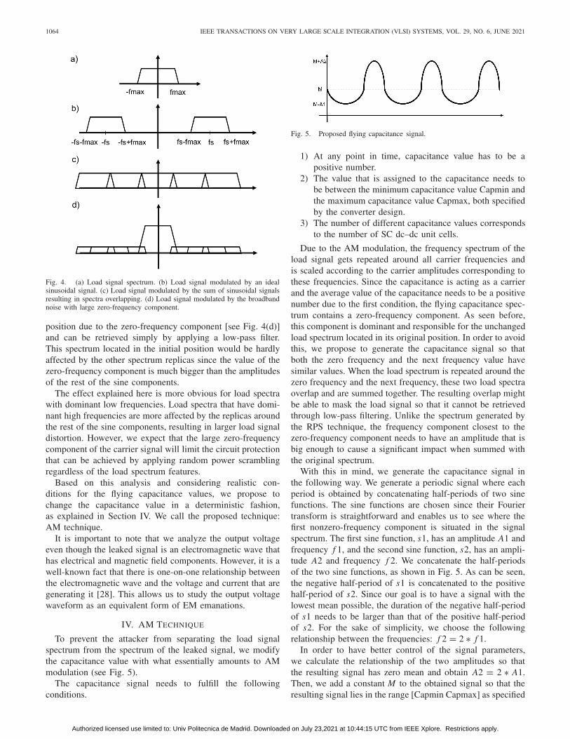
Fig. 4. (a) Load signal spectrum. (b) Load signal modulated by an idealsinusoidal signal. (c) Load signal modulated by the sum of sinusoidal signalsresulting in spectra overlapping. (d) Load signal modulated by the broadbandnoise with large zero-frequency component.
position due to the zero-frequency component [see Fig. 4(d)]and can be retrieved simply by applying a low-pass filter.This spectrum located in the initial position would be hardlyaffected by the other spectrum replicas since the value of thezero-frequency component is much bigger than the amplitudesof the rest of the sine components.
The effect explained here is more obvious for load spectrawith dominant low frequencies. Load spectra that have domi-nant high frequencies are more affected by the replicas aroundthe rest of the sine components, resulting in larger load signaldistortion. However, we expect that the large zero-frequencycomponent of the carrier signal will limit the circuit protectionthat can be achieved by applying random power scramblingregardless of the load spectrum features.
Based on this analysis and considering realistic con-ditions for the flying capacitance values, we propose tochange the capacitance value in a deterministic fashion,as explained in Section IV. We call the proposed technique:AM technique.
It is important to note that we analyze the output voltageeven though the leaked signal is an electromagnetic wave thathas electrical and magnetic field components. However, it is awell-known fact that there is one-on-one relationship betweenthe electromagnetic wave and the voltage and current that aregenerating it [28]. This allows us to study the output voltagewaveform as an equivalent form of EM emanations.
IV. AM TECHNIQUE
To prevent the attacker from separating the load signalspectrum from the spectrum of the leaked signal, we modifythe capacitance value with what essentially amounts to AMmodulation (see Fig. 5).
The capacitance signal needs to fulfill the followingconditions.
Fig. 5. Proposed flying capacitance signal.
1) At any point in time, capacitance value has to be apositive number.
2) The value that is assigned to the capacitance needs tobe between the minimum capacitance value Capmin andthe maximum capacitance value Capmax, both specifiedby the converter design.
3) The number of different capacitance values correspondsto the number of SC dc–dc unit cells.
Due to the AM modulation, the frequency spectrum of theload signal gets repeated around all carrier frequencies andis scaled according to the carrier amplitudes corresponding tothese frequencies. Since the capacitance is acting as a carrierand the average value of the capacitance needs to be a positivenumber due to the first condition, the flying capacitance spec-trum contains a zero-frequency component. As seen before,this component is dominant and responsible for the unchangedload spectrum located in its original position. In order to avoidthis, we propose to generate the capacitance signal so thatboth the zero frequency and the next frequency value havesimilar values. When the load spectrum is repeated around thezero frequency and the next frequency, these two load spectraoverlap and are summed together. The resulting overlap mightbe able to mask the load signal so that it cannot be retrievedthrough low-pass filtering. Unlike the spectrum generated bythe RPS technique, the frequency component closest to thezero-frequency component needs to have an amplitude that isbig enough to cause a significant impact when summed withthe original spectrum.
With this in mind, we generate the capacitance signal inthe following way. We generate a periodic signal where eachperiod is obtained by concatenating half-periods of two sinefunctions. The sine functions are chosen since their Fouriertransform is straightforward and enables us to see where thefirst nonzero-frequency component is situated in the signalspectrum. The first sine function, s1, has an amplitude A1 andfrequency f 1, and the second sine function, s2, has an ampli-tude A2 and frequency f 2. We concatenate the half-periodsof the two sine functions, as shown in Fig. 5. As can be seen,the negative half-period of s1 is concatenated to the positivehalf-period of s2. Since our goal is to have a signal with thelowest mean possible, the duration of the negative half-periodof s1 needs to be larger than that of the positive half-periodof s2. For the sake of simplicity, we choose the followingrelationship between the frequencies: f 2 = 2 ∗ f 1.
In order to have better control of the signal parameters,we calculate the relationship of the two amplitudes so thatthe resulting signal has zero mean and obtain A2 = 2 ∗ A1.Then, we add a constant M to the obtained signal so that theresulting signal lies in the range [Capmin Capmax] as specified
Authorized licensed use limited to: Univ Politecnica de Madrid. Downloaded on July 23,2021 at 10:44:15 UTC from IEEE Xplore. Restrictions apply.

JEVTIC et al.: EM SIDE-CHANNEL COUNTERMEASURE FOR SWITCHED-CAPACITOR DC–DC CONVERTERS 1065
Fig. 6. Spectrum of the proposed flying capacitance signal.
by the second condition. The following equations need to befulfilled:
M − A1 = Capmin
M + A2 = Capmax
A2 = 2 ∗ A1. (3)
Amplitudes of the two sine functions as well as the meanof the generated signal are then calculated as
M = Capmax + 2 ∗ Capmin
3
A1 = Capmax − Capmin
3
A2 = 2 ∗ Capmax − Capmin
3. (4)
Fig. 6 shows an example of the generated signal spectrumfor the following settings: f 1 = 75 Hz, f 2 = 150 Hz,A1 = 313 fF, A2 = 626 fF, and M = 373 fF. It canbe seen that the first nonzero-frequency component has anamplitude that is comparable to the zero-frequency component,so the overlapping of the original spectrum with the shiftedone is more effective. In addition, the position of the firstnonzero-frequency component depends on the frequencies ofthe two sine signals and can be changed easily as to producemore effective overlapping in the resulting spectrum.
Since the generated flying capacitance signal is periodic andthe number of unit cells fixed, there are a limited number ofpossible flying capacitance values. We choose the first flyingcapacitance value randomly out of possible values within oneperiod of the generated signal. Instead of assigning always avalue M as the first capacitance value (see Fig. 5), we mightassign it any other value of the generated signal and start thesignal generation from there. For example, if the first valueis equal to M − A1 or M + A2, the flying capacitance signalis phase shifted by π /3 or 5π /6, respectively. The analysis onthe aliasing in the frequency domain is not affected by thesignal phase shift, while it is ensured that two executions forthe same load and the same moment in time have differentflying capacitance values.
V. SECURITY EVALUATION
We design two sets of experiments. In the first set, we testthe proposed technique for many different loads by calculatingthe correlation coefficient between the load signal and the
Fig. 7. SC dc–dc unit cell implementation.
leaked signal. The goal is to see whether critical informa-tion can be obtained by postprocessing the leaked signal.In the second set, we apply the test vector leakage assessment(TVLA) [25] to calculate the number of leaky points whenthe proposed technique is applied to the circuit. The goal is tosee whether differential and correlation attacks would yieldany significant information from the circuit. These attacksare the most common side-channel attacks and are based onmeasuring many side-channel traces for different input data fortargeted algorithm. Afterward, a statistical test is employed todetermine which secret key most probably caused the leakage.
A. Correlation Coefficient Comparison
In order to test the AM technique for many different loadsand flying capacitance signals, we built our evaluation flow inScilab in the following way.
First, we use Cadence to implement an SC dc–dc converterin 28-nm fully depleted silicon-on-insulator (FDSOI) CMOS.The converter consists of variable number of unit cells andthe control circuitry that was described in Section II. We usethe series–parallel topology for the SC dc–dc implementation.Each unit cell consists of five switches and a flying capacitorto achieve 1/2 ratio between the output and the input voltage,as shown in Fig. 7. Four switches S1–S4 are used for thenormal operation mode of the converter when the converteris switching between phases φ1 and φ2. Switches S1 andS5 are used to connect the flying capacitor between 1 V andVref when the unit cell is not used, ensuring that there is noadditional strain over the switches when the cell is turned on.
We use a decoupling capacitance equal to 80 pF that isestimated to be the capacitance of the microprocessor suppliedby the converter.
Then, we build a simulation flow in Scilab in order toaccelerate the simulations for many different settings for theload and the flying capacitor. We describe the functionalityof the dc–dc converter by using the following differentialequations for the phase φ1 (see Fig. 7):
Vin − Rsw1CflydVc
dt− Vc − Rsw4Cfly
dVc
dt= Vout
CdecdVout
dt= Cfly
dVc
dt− Vout
Rload
(5)
Authorized licensed use limited to: Univ Politecnica de Madrid. Downloaded on July 23,2021 at 10:44:15 UTC from IEEE Xplore. Restrictions apply.
1066 IEEE TRANSACTIONS ON VERY LARGE SCALE INTEGRATION (VLSI) SYSTEMS, VOL. 29, NO. 6, JUNE 2021
Fig. 8. Output voltage waveform from (a) Cadence simulation (top) and(b) Scilab simulation (bottom) for 300-� load.
and the following equations for the phase φ2:
Rsw2CflydVc
dt+ Vc + Rsw3Cfly
dVc
dt= V out
CdecdV out
dt= −Cfly
dVc
dt− V out
Rload(6)
where RswN are the resistances of the switches (N =1, 2, 3, 4), Cfly and Cdec are the values of the flying anddecoupling capacitor, respectively, Vc is the voltage over theflying capacitor, and Vin and Vout are the input and outputvoltages, respectively. We confirm the veracity of the flow bycomparing the Scilab simulation results to the results simulatedin Cadence. Since the comparison is satisfactory (see Fig. 8),from here on, we use the flow built in Scilab to test theeffectiveness of the proposed AM technique.
We start by verifying that (2) can be used to faithfullyrepresent the functionality of the implemented SC dc–dcconverter.
We use AES measured power traces available at [26] togenerate the load that corresponds to the AES execution, andin addition, we design other types of loads to further explorethe effectiveness of the proposed technique. The goal is to findout whether the proposed technique can offer better protectionfor different cryptographic algorithms. In order to simulate theload that corresponds to the execution of any cryptographicalgorithm, we generate the load that fulfills the followingconditions.
1) The load is generated as a periodic signal since most ofcryptographic algorithms are iterative processes with thesame number and type of operations that are executedin each iteration.
2) We generate different load patterns by changing thenumber of different load values in each iteration betweenfour and 100 000.
3) The load current is changing between 50 and 500 μA,values that correspond to the minimum and maximumpower consumption of the microprocessor presented in[20].
For each load, one load pattern is repeated over time in orderto mimic the iterations in the cryptographic algorithms. Thenumber of the different load values corresponds to the numberof different operations that are executed and consume differentpowers. For example, AES algorithm has at least ten rounds.The number of rounds depends on the length of the secretkey. In each round, there are four different actions that arecarried out: Byte Substitution, Shift Rows, Mix Columns, andKey Addition [27]. Each of these actions consists of variousdifferent operations that are used to alter the data. For thisreason, we choose to have at least four different load valuesthat correspond to four different actions. Increasing the numberof different load values corresponds to refining the number ofdifferent current values needed for each operation.
For each load pattern, we simulate the SC dc–dc converterwith the corresponding load attached to its output voltage.We postprocess the output voltage signal by applying naturallogarithm and applying derivative, as explained in Section III.We then take the reciprocal of the obtained derivative andmultiply it with −1 in order to obtain the exact expression onthe right-hand side of (2). In addition, we filter the resultingsignal since the output voltage has discontinuity wheneverthere is a switch between the phases of the converter. Whenderivative is applied to the switch between the phases, it resultsin large peaks. These peaks can affect the cross correlationcoefficient significantly, so we use a median filter to smoothout the postprocessed output voltage.
Finally, we compare the signals R(t) ∗ C(t) and the post-processed output voltage, by calculating the cross correlationcoeffient between them. We repeat the simulations for manydifferent load patterns and different settings for the flyingcapacitor values. In all cases, the coefficient is very close toone, thus validating (2).
Fig. 9 shows an example for the waveforms of the outputvoltage, the postprocessed output voltage (i.e., the voltage afterapplying natural logarithm, derivative, and the negative recip-rocal), filtered postprocessed output voltage, and the productof the load and the capacitance values. It can be seen thatthe filtered postprocessed output voltage is perfectly correlatedwith R(t)∗C(t) as expected from their correlation coefficient.Therefore, from here on, we calculate the cross correlationcoefficient directly between the load R(t) and R(t) ∗ C(t)for all the experiments designed to validate the effectivenessof the proposed side-channel countermeasures. The measuredAES load has 16 000 traces [26]. For the rest of the loads,we generate 36 000 samples for the load signal, in orderto make sure that the resulting coefficients are statisticallycorrect.
We start by evaluating the RPS technique. We set thereference voltage to 0.4 V and randomly change the valueof the flying capacitor between 60 pF and 1 nF. Scilab funtiongrand(), used for pseudorandom number generation, assignsrandom values to the flying capacitor. To give an example of
Authorized licensed use limited to: Univ Politecnica de Madrid. Downloaded on July 23,2021 at 10:44:15 UTC from IEEE Xplore. Restrictions apply.
JEVTIC et al.: EM SIDE-CHANNEL COUNTERMEASURE FOR SWITCHED-CAPACITOR DC–DC CONVERTERS 1067
Fig. 9. Waveforms for output voltage, postprocessed output voltage, filteredpostprocessed output voltage, and R(t) ∗ C(t).
Fig. 10. Output voltage signal (top), load (middle), and flying capacitance(bottom).
the RPS waveforms, Fig. 10 shows the output voltage, the loadthat corresponds to the pattern six and the flying capacitorvalue. The pattern six refers to six different load values ineach iteration. For each load pattern, we generate five differentloads.
The cross correlation coefficients are calculated betweenthe load signal R(t) and the signal R(t) ∗ C(t) after it hasbeen passed through a low-pass filter. The cross correlationcoefficients for all load patterns are presented in Fig. 11. It canbe seen that they are close to one for all generated loads. Asmentioned before, this is due to the zero-frequency componentof the flying capacitance. The spectra of the load, flyingcapacitor, and the product of the two are presented in Fig. 12where this effect is visually represented. Due to the dominantzero-frequency component, random power scrambling is notappreciated in this figure. For this reason, this figure has beenzoomed in and represented in Fig. 13. It can be seen that theleaked signal spectrum has additional noise due to the randompower scrambling. However, this additional noise is too smallto mask the original load spectrum.
For AES load, the coefficients drop to 0.6 measured powertraces for AES execution have dominant high-frequency com-ponent since the current peaks occur on the rising clockedge when the flip-flops change their state. Hence, the high-frequency part of the original load spectrum will be affectedmore by the other load replicas, resulting in a lower coefficientbetween the load and the leaked signal.
We then evaluate the AM technique proposed in thisarticle. The settings for the reference value, minimum and
Fig. 11. Cross correlation coefficient for the RPS technique.
Fig. 12. Fast Fourier transformation (FFT) for load (top), flying capacitance(middle), and the convolution of the two (bottom) for the RPS technique.
Fig. 13. Fig. 12 zoomed in.
maximum capacitance value, and the cross correlation com-putation method are the same as in the first case. The flyingcapacitance value is changed according to the signal generated,as explained in Section IV. We swipe the frequency of thegenerated signal (i.e., frequency f 1 and consequently f 2 of
Authorized licensed use limited to: Univ Politecnica de Madrid. Downloaded on July 23,2021 at 10:44:15 UTC from IEEE Xplore. Restrictions apply.
1068 IEEE TRANSACTIONS ON VERY LARGE SCALE INTEGRATION (VLSI) SYSTEMS, VOL. 29, NO. 6, JUNE 2021
Fig. 14. Cross correlation coefficient for the AM technique.
Fig. 15. FFT for load (top), flying capacitance (middle), and the convolutionof the two (bottom) for the AM technique.
the generated signal presented in Fig. 5) in order to find theone that produces the lowest cross correlation coefficient.
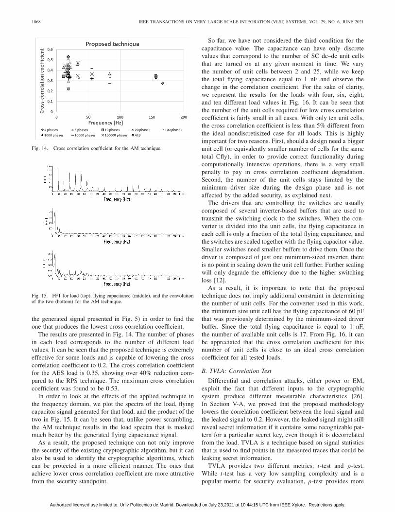
The results are presented in Fig. 14. The number of phasesin each load corresponds to the number of different loadvalues. It can be seen that the proposed technique is extremelyeffective for some loads and is capable of lowering the crosscorrelation coefficient to 0.2. The cross correlation coefficientfor the AES load is 0.35, showing over 40% reduction com-pared to the RPS technique. The maximum cross correlationcoefficient was found to be 0.53.
In order to look at the effects of the applied technique inthe frequency domain, we plot the spectra of the load, flyingcapacitor signal generated for that load, and the product of thetwo in Fig. 15. It can be seen that, unlike power scrambling,the AM technique results in the load spectra that is maskedmuch better by the generated flying capacitance signal.
As a result, the proposed technique can not only improvethe security of the existing cryptographic algorithm, but it canalso be used to identify the cryptographic algorithms, whichcan be protected in a more efficient manner. The ones thatachieve lower cross correlation coefficient are more attractivefrom the security standpoint.
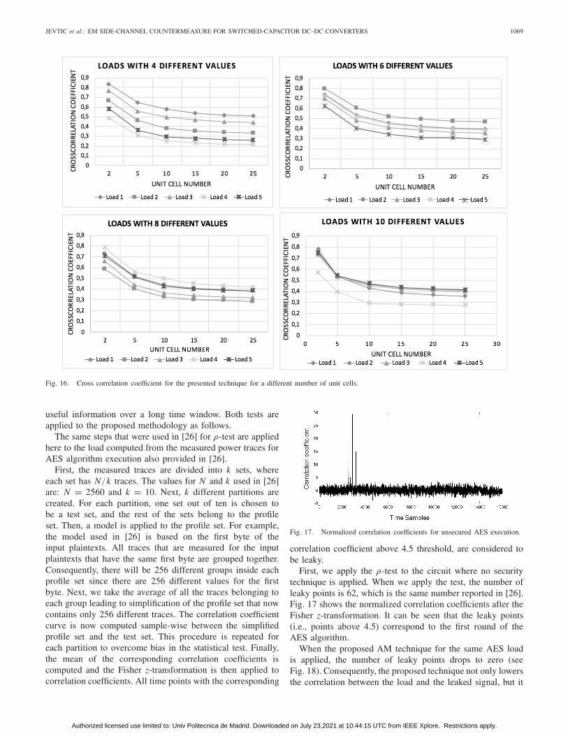
So far, we have not considered the third condition for thecapacitance value. The capacitance can have only discretevalues that correspond to the number of SC dc–dc unit cellsthat are turned on at any given moment in time. We varythe number of unit cells between 2 and 25, while we keepthe total flying capacitance equal to 1 nF and observe thechange in the correlation coefficient. For the sake of clarity,we represent the results for the loads with four, six, eight,and ten different load values in Fig. 16. It can be seen thatthe number of the unit cells required for low cross correlationcoefficient is fairly small in all cases. With only ten unit cells,the cross correlation coefficient is less than 5% different fromthe ideal nondiscretisized case for all loads. This is highlyimportant for two reasons. First, should a design need a biggerunit cell (or equivalently smaller number of cells for the sametotal Cfly), in order to provide correct functionality duringcomputationally intensive operations, there is a very smallpenalty to pay in cross correlation coefficient degradation.Second, the number of the unit cells stays limited by theminimum driver size during the design phase and is notaffected by the added security, as explained next.
The drivers that are controlling the switches are usuallycomposed of several inverter-based buffers that are used totransmit the switching clock to the switches. When the con-verter is divided into the unit cells, the flying capacitance ineach cell is only a fraction of the total flying capacitance, andthe switches are scaled together with the flying capacitor value.Smaller switches need smaller buffers to drive them. Once thedriver is composed of just one minimum-sized inverter, thereis no point in scaling down the unit cell further. Further scalingwill only degrade the efficiency due to the higher switchingloss [12].
As a result, it is important to note that the proposedtechnique does not imply additional constraint in determiningthe number of unit cells. For the converter used in this work,the minimum size unit cell has the flying capacitance of 60 pFthat was previously determined by the minimum-sized driverbuffer. Since the total flying capacitance is equal to 1 nF,the number of available unit cells is 17. From Fig. 16, it canbe appreciated that the cross correlation coefficient for thisnumber of unit cells is close to an ideal cross correlationcoefficient for all tested loads.
B. TVLA: Correlation Test
Differential and correlation attacks, either power or EM,exploit the fact that different inputs to the cryptographicsystem produce different measurable characteristics [26].In Section V-A, we proved that the proposed methodologylowers the correlation coefficient between the load signal andthe leaked signal to 0.2. However, the leaked signal might stillreveal secret information if it contains some recognizable pat-tern for a particular secret key, even though it is decorrelatedfrom the load. TVLA is a technique based on signal statisticsthat is used to find points in the measured traces that could beleaking secret information.
TVLA provides two different metrics: t-test and ρ-test.While t-test has a very low sampling complexity and is apopular metric for security evaluation, ρ-test provides more
Authorized licensed use limited to: Univ Politecnica de Madrid. Downloaded on July 23,2021 at 10:44:15 UTC from IEEE Xplore. Restrictions apply.
JEVTIC et al.: EM SIDE-CHANNEL COUNTERMEASURE FOR SWITCHED-CAPACITOR DC–DC CONVERTERS 1069
Fig. 16. Cross correlation coefficient for the presented technique for a different number of unit cells.
useful information over a long time window. Both tests areapplied to the proposed methodology as follows.
The same steps that were used in [26] for ρ-test are appliedhere to the load computed from the measured power traces forAES algorithm execution also provided in [26].
First, the measured traces are divided into k sets, whereeach set has N/k traces. The values for N and k used in [26]are: N = 2560 and k = 10. Next, k different partitions arecreated. For each partition, one set out of ten is chosen tobe a test set, and the rest of the sets belong to the profileset. Then, a model is applied to the profile set. For example,the model used in [26] is based on the first byte of theinput plaintexts. All traces that are measured for the inputplaintexts that have the same first byte are grouped together.Consequently, there will be 256 different groups inside eachprofile set since there are 256 different values for the firstbyte. Next, we take the average of all the traces belonging toeach group leading to simplification of the profile set that nowcontains only 256 different traces. The correlation coefficientcurve is now computed sample-wise between the simplifiedprofile set and the test set. This procedure is repeated foreach partition to overcome bias in the statistical test. Finally,the mean of the corresponding correlation coefficients iscomputed and the Fisher z-transformation is then applied tocorrelation coefficients. All time points with the corresponding
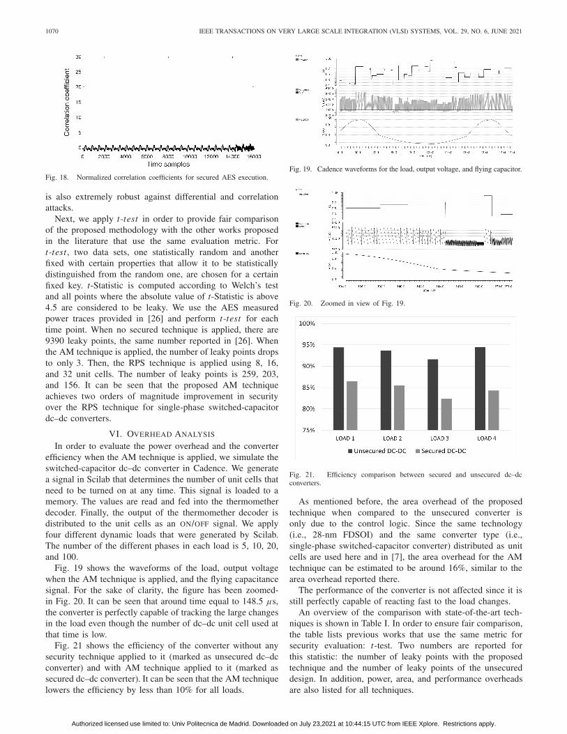
Fig. 17. Normalized correlation coefficients for unsecured AES execution.
correlation coefficient above 4.5 threshold, are considered tobe leaky.
First, we apply the ρ-test to the circuit where no securitytechnique is applied. When we apply the test, the number ofleaky points is 62, which is the same number reported in [26].Fig. 17 shows the normalized correlation coefficients after theFisher z-transformation. It can be seen that the leaky points(i.e., points above 4.5) correspond to the first round of theAES algorithm.
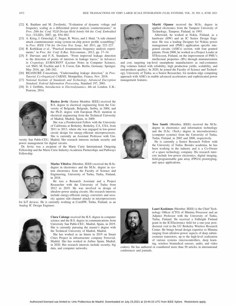
When the proposed AM technique for the same AES loadis applied, the number of leaky points drops to zero (seeFig. 18). Consequently, the proposed technique not only lowersthe correlation between the load and the leaked signal, but it
Authorized licensed use limited to: Univ Politecnica de Madrid. Downloaded on July 23,2021 at 10:44:15 UTC from IEEE Xplore. Restrictions apply.
1070 IEEE TRANSACTIONS ON VERY LARGE SCALE INTEGRATION (VLSI) SYSTEMS, VOL. 29, NO. 6, JUNE 2021
Fig. 18. Normalized correlation coefficients for secured AES execution.
is also extremely robust against differential and correlationattacks.
Next, we apply t-test in order to provide fair comparisonof the proposed methodology with the other works proposedin the literature that use the same evaluation metric. Fort-test , two data sets, one statistically random and anotherfixed with certain properties that allow it to be statisticallydistinguished from the random one, are chosen for a certainfixed key. t-Statistic is computed according to Welch’s testand all points where the absolute value of t-Statistic is above4.5 are considered to be leaky. We use the AES measuredpower traces provided in [26] and perform t-test for eachtime point. When no secured technique is applied, there are9390 leaky points, the same number reported in [26]. Whenthe AM technique is applied, the number of leaky points dropsto only 3. Then, the RPS technique is applied using 8, 16,and 32 unit cells. The number of leaky points is 259, 203,and 156. It can be seen that the proposed AM techniqueachieves two orders of magnitude improvement in securityover the RPS technique for single-phase switched-capacitordc–dc converters.
VI. OVERHEAD ANALYSIS
In order to evaluate the power overhead and the converterefficiency when the AM technique is applied, we simulate theswitched-capacitor dc–dc converter in Cadence. We generatea signal in Scilab that determines the number of unit cells thatneed to be turned on at any time. This signal is loaded to amemory. The values are read and fed into the thermometherdecoder. Finally, the output of the thermomether decoder isdistributed to the unit cells as an ON/OFF signal. We applyfour different dynamic loads that were generated by Scilab.The number of the different phases in each load is 5, 10, 20,and 100.
Fig. 19 shows the waveforms of the load, output voltagewhen the AM technique is applied, and the flying capacitancesignal. For the sake of clarity, the figure has been zoomed-in Fig. 20. It can be seen that around time equal to 148.5 μs,the converter is perfectly capable of tracking the large changesin the load even though the number of dc–dc unit cell used atthat time is low.
Fig. 21 shows the efficiency of the converter without anysecurity technique applied to it (marked as unsecured dc–dcconverter) and with AM technique applied to it (marked assecured dc–dc converter). It can be seen that the AM techniquelowers the efficiency by less than 10% for all loads.
Fig. 19. Cadence waveforms for the load, output voltage, and flying capacitor.
Fig. 20. Zoomed in view of Fig. 19.
Fig. 21. Efficiency comparison between secured and unsecured dc–dcconverters.
As mentioned before, the area overhead of the proposedtechnique when compared to the unsecured converter isonly due to the control logic. Since the same technology(i.e., 28-nm FDSOI) and the same converter type (i.e.,single-phase switched-capacitor converter) distributed as unitcells are used here and in [7], the area overhead for the AMtechnique can be estimated to be around 16%, similar to thearea overhead reported there.
The performance of the converter is not affected since it isstill perfectly capable of reacting fast to the load changes.
An overview of the comparison with state-of-the-art tech-niques is shown in Table I. In order to ensure fair comparison,the table lists previous works that use the same metric forsecurity evaluation: t-test. Two numbers are reported forthis statistic: the number of leaky points with the proposedtechnique and the number of leaky points of the unsecureddesign. In addition, power, area, and performance overheadsare also listed for all techniques.
Authorized licensed use limited to: Univ Politecnica de Madrid. Downloaded on July 23,2021 at 10:44:15 UTC from IEEE Xplore. Restrictions apply.

JEVTIC et al.: EM SIDE-CHANNEL COUNTERMEASURE FOR SWITCHED-CAPACITOR DC–DC CONVERTERS 1071
TABLE I
COMPARISON OF AM TECHNIQUE WITH EXISTING COUNTERMEASURES
It can be seen that the proposed methodology achievesreduction in t-statistic is 99.93% while incurring no per-formance degradation and increasing power consumption byonly 15% and area by 16%, compared to the unsecureddesign without voltage regulators. Consequently, an excellenttradeoff between the added security and converter power, area,and performance makes the proposed technique an attractivesolution for protection from EM side-channel attacks.
VII. CONCLUSION
We have presented a novel technique for single-phase SCdc–dc converters to improve the security of the IoT devicesagainst side-channel attacks. The technique relies on detailedphysical mechanisms of the leaked signal and it is basedon the AM of the load current by the flying capacitancethat acts as a carrier. The capacitance is changed in a deter-ministic fashion in order to achieve overlapping of the loadspectrum in the leaked signal spectrum. The results showthat the technique can lower the cross correlation coefficientbetween the leaked signal and the load to below 0.2. Thenumber of SC dc–dc unit cells that are needed to achieve lowcorrelation coefficients is below the limit set by the design,resulting in no additional impact on the power density ofthe converter. When the statistical test based on TVLA isapplied to the protected circuit, the number of leaky pointsis reduced to zero, indicating an excellent robustness againstdifferential and correlation attacks. The presented methodol-ogy lowers the converter efficiency by less than 10% andhas a minimal impact on the area and performance of theconverter.
ACKNOWLEDGMENT
The authors would like to thank Prof. Mariano Garcia Oterofrom the Technical University of Madrid for his help onevaluation metric.
REFERENCES
[1] D. Agrawal et al., “The EM side-channel(s): Attacks and assessmentmethodologies,” in Proc. CHES, in Lecture Notes in Computer Science,vol. 2523, 2002, pp. 29–45.
[2] D. Das et al., “Ground-up root-cause analysis guided low-overheadgeneric countermeasure for electro-magnetic side-channel attack,” Crip-tology ePrint Arch., Tech. Rep. 2018/620, 2018, p. 620.
[3] R. Callan, A. Zajic, and M. Prvulovic, “FASE: Finding amplitude-modulated side-channel emanations,” in Proc. 42nd Annu. Int. Symp.Comput. Archit. (ISCA), Jun. 2015, pp. 592–603.
1The number of traces for t-test is not reported, but the number of tracesused for correlation coefficient is over 1 million.
[4] L. Sauvage, S. Guilley, and Y. Mathieu, “Electromagnetic radiationsof FPGAs: High spatial resolution cartography and attack on a crypto-graphic module,” ACM Trans. Comput. Logic, vol. 2, no. 1, pp. 1–24,Aug. 2008, Art. no. 4.
[5] P. Maistri, S. Tiran, P. Maurine, I. Koren, and R. Leveugle, “Countermea-sures against EM analysis for a secured FPGA-based AES implementa-tion,” in Proc. Int. Conf. Reconfigurable Comput. FPGAs (ReConFig),Dec. 2013, pp. 1–6.
[6] R. Jevtic et al., “Per-core DVFS for many-core processors in 28 nmFDSOI technology,” IEEE Trans. Very Large Scale Integr. (VLSI) Syst.,vol. 23, no. 4, pp. 723–730, Apr. 2015.
[7] B. Zimmer et al., “A RISC-V vector processor with simultaneous-switching switched-capacitor DC–DC converters in 28 nm FDSOI,”IEEE J. Solid-State Circuits, vol. 51, no. 4, pp. 930–942, Apr. 2016.
[8] M. Turnquist et al., “Fully integrated DC-DC converter and a 0.4V 32-bitCPU with timing-error prevention supplied from a prototype 1.55V Li-ion battery,” in Proc. Symp. VLSI Circuits (VLSI Circuits), Jun. 2015,pp. C320–C321.
[9] A. Singh, M. Kar, S. K. Mathew, A. Rajan, V. De, andS. Mukhopadhyay, “Improved power/EM side-channel attack resistanceof 128-bit AES engines with random fast voltage dithering,” IEEE J.Solid-State Circuits, vol. 54, no. 2, pp. 569–583, Feb. 2019.
[10] A. Singh, M. Kar, S. Mathew, A. Rajan, V. De, and S. Mukhopadhyay,“25.3 A 128b AES engine with higher resistance to power and elec-tromagnetic side-channel attacks enabled by a security-aware integratedall-digital low-dropout regulator,” in IEEE Int. Solid-State Circuits Conf.(ISSCC) Dig. Tech. Papers, Feb. 2019, pp. 404–406.
[11] D. Kamel et al, “Towards securing low-power digital circuits with ultra-low-voltage Vdd randomizers,” in Proc. Int. Conf. Secur., Privacy, Appl.Cryptogr. Eng., 2016, pp. 233–248.
[12] H.-P. Le, S. R. Sanders, and E. Alon, “Design techniques for fullyintegrated switched-capacitor DC-DC converters,” IEEE J. Solid-StateCircuits, vol. 46, no. 9, pp. 2120–2131, Sep. 2011.
[13] O. A. Uzun and S. Kose, “Converter-gating: A power efficient and secureon-chip power delivery system,” IEEE J. Emerg. Sel. Topics CircuitsSyst., vol. 4, no. 2, pp. 169–179, Jun. 2014.
[14] W. Yu and S. Kose, “Charge-withheld converter-reshuffling: A counter-measure against power analysis attacks,” IEEE Trans. Circuits Syst. II,Exp. Briefs, vol. 63, no. 5, pp. 438–442, May 2016.
[15] R. Jevtic, M. Ylitolva, and L. Koskinen, “Reconfigurable switchedcapacitor DC-DC converter for improved security in IoT devices,”in Proc. 28th Int. Symp. Power Timing Modeling, Optim. Simulation(PATMOS), Jul. 2018.
[16] A. Ghosh, D. Das, and S. Sen, “Physical time-varying transfer func-tions as generic low-overhead power-SCA countermeasure,” 2020,arXiv:2003.07440. [Online]. Available: http://arxiv.org/abs/2003.07440
[17] D. Das et al., “27.3 EM and power SCA-resilient AES-256 in 65 nmCMOS through >350X current-domain signature attenuation,” in IEEEInt. Solid-State Circuits Conf. (ISSCC) Dig. Tech. Papers, Feb. 2020,pp. 424–426.
[18] C. Tokunaga and D. Blaauw, “Securing encryption systems with aswitched capacitor current equalizer,” IEEE J. Solid-State Circuits,vol. 45, no. 1, pp. 23–31, Jan. 2010.
[19] C. Wang, Y. Cai, H. Wang, and Q. Zhou, “Electromagnetic equalizer:An active countermeasure against EM side-channel attack,” in Proc. Int.Conf. Comput.-Aided Design (ICCAD), Nov. 2018, pp. 1–8.
[20] M. Hiienkari et al., “A 3.15 pJ/cyc 32-bit RISC CPU with timing-errorprevention and adaptive clocking in 28 nm CMOS,” in Proc. IEEECustom Integr. Circuits Conf. (CICC), Sep. 2014, pp. 1–4.
[21] F. U. Rahman et al., “A unified clock and switched-capacitor-basedpower delivery architecture for variation tolerance in low-voltage SoCdomains,” IEEE J. Solid-State Circuits, vol. 54, no. 4, pp. 1173–1184,Apr. 2019.
Authorized licensed use limited to: Univ Politecnica de Madrid. Downloaded on July 23,2021 at 10:44:15 UTC from IEEE Xplore. Restrictions apply.
1072 IEEE TRANSACTIONS ON VERY LARGE SCALE INTEGRATION (VLSI) SYSTEMS, VOL. 29, NO. 6, JUNE 2021
[22] K. Baddam and M. Zwolinski, “Evaluation of dynamic voltage andfrequency scaling as a differential power analysis countermeasure,” inProc. 20th Int. Conf. VLSI Design Held Jointly 6th Int. Conf. EmbeddedSyst. (VLSID), 2007, pp. 854–862.
[23] A. Krieg, J. Grinschgl, C. Steger, R. Weiss, and J. Haid, “A side channelattack countermeasure using system-on-chip power profile scrambling,”in Proc. IEEE 17th Int. On-Line Test. Symp., Jul. 2011, pp. 222–227.
[24] R. Korkikian et al., “Practical instantaneous frequency analysis experi-ments,” in Proc. Int. Conf. E-Bus. Telecommun., 2013, pp. 17–34.
[25] F. Durvaux and F.-X. Standaert, “From improved leakage detectionto the detection of points of interests in leakage traces,” in Advancesin Cryptology EUROCRYPT (Lecture Notes in Computer Science),vol. 9665, M. Fischlin and J. S. Coron, Eds. Berlin, Germany: Springer,May 2016, pp. 240–262.
[26] REASSURE Consortium, “Understanding leakage detection,” in Proc.Tutorial Co-Organized CARDIS, Montpellier, France, Nov. 2018.
[27] National Institute of Standards and Technology. Advanced EncryptionStandard. Federal Information Processing, Standard 197, 2001.
[28] D. J. Griffiths, Introduction to Electrodynamics, 4th ed. London, U.K.:Pearson, 2014.
Ruzica Jevtic (Senior Member, IEEE) received theB.S. degree in electrical engineering from the Uni-versity of Belgrade, Belgrade, Serbia, in 2004, andthe Ph.D. degree with European Ph.D. mention inelectrical engineering from the Technical Universityof Madrid, Madrid, Spain, in 2009.
She was a Postdoctoral Fellow with the Universityof California at Berkeley, Berkeley, CA, USA, from2011 to 2013, where she was engaged in low-powercircuit design for energy-efficient microprocessors.She is currently an Assistant Professor with Uni-
versity San Pablo-CEU, Madrid. Her research interests include security andpower management for digital circuits.
Dr. Jevtic was a recipient of the Marie Curie International OutgoingFellowship and the Marie Curie Industry-Academia Partnerships and PathwaysFellowship.
Marko Ylitolva (Member, IEEE) received the B.Sc.degree in electronics and the M.Sc. degree in sys-tem electronics from the Faculty of Science andEngineering, University of Turku, Turku, Finland,in 2018.
He was a Research Assistant and a ProjectResearcher with the University of Turku from2012 to 2019. He was involved in design ofultralow-power analog circuits. His research interestsinclude energy-efficient energy converters and secu-rity against side-channel attacks in microprocessors
for IoT devices. He is currently working at CoreHW, Turku, Finland, as anAnalog IC Design Engineer.
Clara Calonge received the B.S. degree in computerscience and the B.S. degree in communications fromUniversity San Pablo-CEU, Madrid, Spain, in 2019.She is currently pursuing the master’s degree withthe Technical University of Madrid, Madrid.
She has worked as an Intern in 2019 on SmartCities Project in infrastructure company Ferrovial,Madrid. She has worked in Airbus Spain, Madrid,in 2020. Her research interests include security, bigdata, and computer networks.
Martti Ojanen received the M.Sc. degree inapplied electronics from the Tampere University ofTechnology, Tampere, Finland, in 1993.
Afterward, he worked at Nokia, Finland, as ahardware (HW) and an IC Senior Design Engi-neer. He was a leading Designer for Nokias powermanagement unit (PMU) application specific inte-grated circuits (ASICs) section, with four grantedpatents. From 2008, he worked as a Project Leader atSTEricsson, Finland, on the improvement of PMU’sintellectual properties (IPs) through miniaturization
and cost, targeting top-level smartphone manufacturers as end-costumers(big volumes linked with reliability, high production yields, scalability, andend-products quality). In 2020, he joined the Faculty of Science and Technol-ogy, University of Turku, as a Senior Researcher, for modern edge computingapproach with ASICs to enable advanced accelerators and sophisticated powermanagement features.
Tero Santti (Member, IEEE) received the M.Sc.degree in electronics and information technologyand the D.Sc. (Tech.) degree in microelectronics(computer systems) from the University of Turku,Turku, Finland, in 2002 and 2008, respectively.
He is currently a Senior Research Fellow withthe University of Turku. Besides academia, he hasbeen working in the industry and is a Co-Ownerof a space technology company. His research inter-ests include low-power electronics, digital imaging,field-programmable gate array (FPGA) prototyping,and space applications.
Lauri Koskinen (Member, IEEE) is the Chief Tech-nology Officer (CTO) of Minima Processor and anAdjunct Professor with the University of Turku,Turku, Finland. He received a Fulbright Finlandgrant in the IC/Electronics field for a one-year post-doctoral visit to the UC Berkeley Wireless ResearchCenter. He brings broad design expertise to Minimaranging from ultralow-power aspects of deep submi-crometer transistors, up to the high-level realizationof various systems (microcontrollers, deep learn-ing, wireless biomedical sensors, audio, and video
coders). He has authored or coauthored more than 50 articles in internationalconferences and journals.
Authorized licensed use limited to: Univ Politecnica de Madrid. Downloaded on July 23,2021 at 10:44:15 UTC from IEEE Xplore. Restrictions apply.