Embed Size (px)
Citation preview
Switched Capacitor Cell Based Dc-dc and Dc-ac Converters
Ke Zou [email protected]
Mark J. Scott [email protected]
Jin Wang [email protected]
Abstract— This paper introduces a modular converter topology based on switched capacitor cells. Two types of cells are discussed in this paper. The full cell switched capacitor structure, which can be used in dc/ac inversion and the half cell structure that has applications in both dc/dc and dc/ac conversion. There are several merits to this converter topology; it has a modular structure, the capacitor count is minimized, and with dc/ac converter there is good redundancy. When utilized as a dc/dc converter, the required output capacitance is minimized and soft switching can be achieved. The basic analysis, simulation results and experimental results on a 1 kW cell prototype are presented.
I. INTRODUCTION Industry continues to push for power electronic devices
that have increased reliability, operate under harsher conditions, with greater power density, all while maintaining a competitive price. One major hurdle in satisfying these needs is the passive components used in energy storage. It is for this reason that interest is growing in switched-capacitor structures. The beauty of switched-capacitor circuits is that power conversion is achieved using only capacitors and switching devices. The absence of magnetic components enables the designer to shrink the system volume, and this is a reason why these circuit have been utilize heavily in low power circuits [1]-[2].
The trend is to build switched-capacitors dc/dc converters with higher power ratings [4]-[5]. However, several issues need to be address when considering these designs: 1) large voltage ripple typical associate the output, 2) pulsing current that results from charging and discharge the energy storage elements, and 3) the EMI produced from these phenomenon [1,3,7]. The first problem can be overcome by installing a large capacitor bank on the output. There are several disadvantages to this, most importantly is that the size of the converter increases. The other two problems mentioned above can be mitigated by utilizing soft-switching.
A modular structure type called a “multilevel modular capacitor-clamped dc–dc converter” is presented in [6]. One advantage of this circuit is that the output can be scaled by increasing or decreasing the number of blocks connected
together and bi-directional power flow is possible, but this circuit still suffers the losses corresponding to hard switching. Also, the capacitor in different modules needs to withstand different voltage stress and one large output capacitor rated at overall output voltage is needed.
To achieve soft-switching, two methods have been used. The first is to integrate an inductor into the switched capacitor circuit [3]. However, as pointed out in [7,11], several of the merits of switch-capacitor circuit are lost once an inductor is added to the circuit. The other method employs the stray inductance from the PCB to form resonant tanks with the capacitors used for energy storage [7, 10].
For the dc/ac application, a method of using an H-bridge after the front switched capacitor dc/dc converter is used in [8]. A multi-level structure derived from traditional high voltage Marx generator is introduced in [12]. The advantage of this circuit is that high ac output can be generated just from one low dc input voltage.
This paper begins by analyzing the switched capacitor converter as a network of basic switching cells. Two basic cells, full cell and half cell switched capacitor are presented. With this knowledge, a switched-capacitor dc/dc circuit is proposed. The advantages of the proposed circuit include modular structure, minimized total capacitor count and largely reduced output capacitance. Also, zero-current-switching and zero-voltage switching can be achieved.
The switched capacitor multilevel inverter is also proposed based on both the full switching cell and half switching cell. This inverter functions similar to the Marx multilevel inverter and possess the same advantages.
Both DC-DC converters and DC-AC inverters are analyzed. Simulation and experimental results are provided. The future goal for this work is to incorporate the switching cell concept into converters and inverters that are created with GaN and SiC devices.
II. BASIC SWITCHING CELLS One approach to creating switched-capacitor circuits is to
cascade switching cells together. At least two different cell
The Department of Electrical and Computer Engineering The Ohio State University
Columbus, Ohio
224U.S. Government work not protected by U.S. copyright
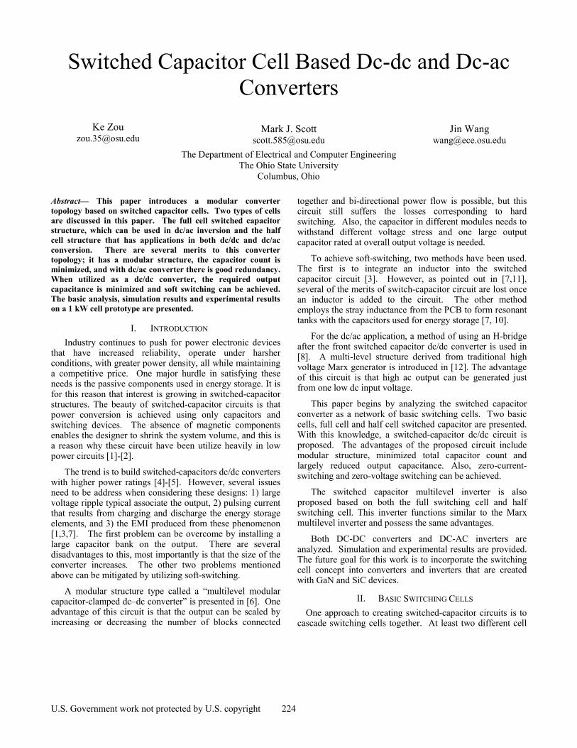
structures are available; the full cell switched-capacitor structure, and the half cell switched-capacitor structure. The full cell structure is shown in Fig.1 (a). It is a four port system that is comprised of four switches and one capacitor. The half cell switched-capacitor structure, shown in Fig.1 (b), is created using only three switches and one capacitor.
By using these blocks, a converter can be realized by connecting N cell structures in series as shown in Fig.1 (c). In this configuration, the capacitor in each cell is charged by the previous stage, and it will be discharged to the cell connected in the proceeding stage. To reduce the current stress of central cells, it is recommended to put cells symmetrically on both side of the dc source, as in Fig.1 (d). For high power applications, on each side of the dc source, it is better to limit n to less or equal to 4.
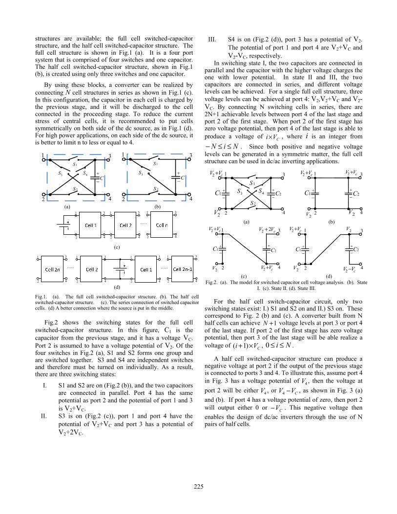
Fig.2 shows the switching states for the full cell
switched-capacitor structure. In this figure, C1 is the capacitor from the previous stage, and it has a voltage VC. Port 2 is assumed to have a voltage potential of V2. Of the four switches in Fig.2 (a), S1 and S2 forms one group and are switched together. S3 and S4 are independent switches and therefore must be turned on individually. As a result, there are three switching states:
I. S1 and S2 are on (Fig.2 (b)), and the two capacitors are connected in parallel. Port 4 has the same potential as port 2 and the potential of port 1 and 3 is V2+VC.
II. S3 is on (Fig.2 (c)), port 1 and port 4 have the potential of V2+VC and port 3 has a potential of V2+2VC.
III. S4 is on (Fig.2 (d)), port 3 has a potential of V2. The potential of port 1 and port 4 are V2+VC and V2-VC, respectively.
In switching state I, the two capacitors are connected in parallel and the capacitor with the higher voltage charges the one with lower potential. In state II and III, the two capacitors are connected in series, and different voltage levels can be achieved. For a single full cell structure, three voltage levels can be achieved at port 4: V2,V2+VC and V2-VC. By connecting N switching cells in series, there are 2N+1 achievable levels between port 4 of the last stage and port 2 of the first stage. When port 2 of the first stage has zero voltage potential, then port 4 of the last stage is able to produce a voltage of CVi × , where i is an integer from
NiN ≤≤− . Since both positive and negative voltage levels can be generated in a symmetric matter, the full cell structure can be used in dc/ac inverting applications.
For the half cell switch-capacitor circuit, only two
switching states exist: I.) S1 and S2 on and II.) S3 on. These correspond to Fig. 2 (b) and (c). A converter built from N half cells can achieve 1+N voltage levels at port 3 or port 4 of the last stage. If port 2 of the first stage has zero voltage potential, then port 3 of the last stage will be able realize a voltage of CVi ×+ )1( , Ni ≤≤0 .
A half cell switched-capacitor structure can produce a negative voltage at port 2 if the output of the previous stage is connected to ports 3 and 4. To illustrate this, assume port 4 in Fig. 3 has a voltage potential of 4V , then the voltage at port 2 will be either 4V , or CVV −4 , as shown in Fig. 3 (a) and (b). If port 4 has a voltage potential of zero, then port 2 will output either 0 or CV− . This negative voltage then enables the design of dc/ac inverters through the use of N pairs of half cells.
1S
2S
3S 4S
1
2
3
+
−
4
2C+
−1C
1
2
3
+
−
4
2C+
−1C
cVV +2
2V
cVV +2
2V 2V
cVV +2
(a) (b)
1
2
3
+
−
4
2C+
−1C
2V
cVV +2
cVV +2
cVV 22 + 1
2
3
+
−
4
2C+
−1C
cVV +2
2V
2V
cVV −2 (c) (d) Fig.2. (a). The model for switched capacitor cell voltage analysis. (b). State
I. (c). State II. (d). State III.
1S
2S
3S 4S
1
2
3
+
−
4
C
1S
2S
3S
1
2
3
+
−
4
C
(a) (b)
1
2
3
4
1
2
3
4
1
2
3
4 (c)
1
2
3
4
1
2
3
4
1
2
3
4
1
2
3
4
(d)
Fig.1. (a). The full cell switched-capacitor structure. (b). The half cell switched-capacitor structure. (c). The series connection of switched capacitorcells. (d) A better connection where the source is put in the middle.
225
1
2
3
+
−
4
2C+
−1C
cVV−4
1
2
3
+
−
4
2C+
−1C
cVV +4
4V 4V
cVV +4 cVV +4
4V
4V
Fig. 3. The two switching states when half cell is used to generate negative voltage.
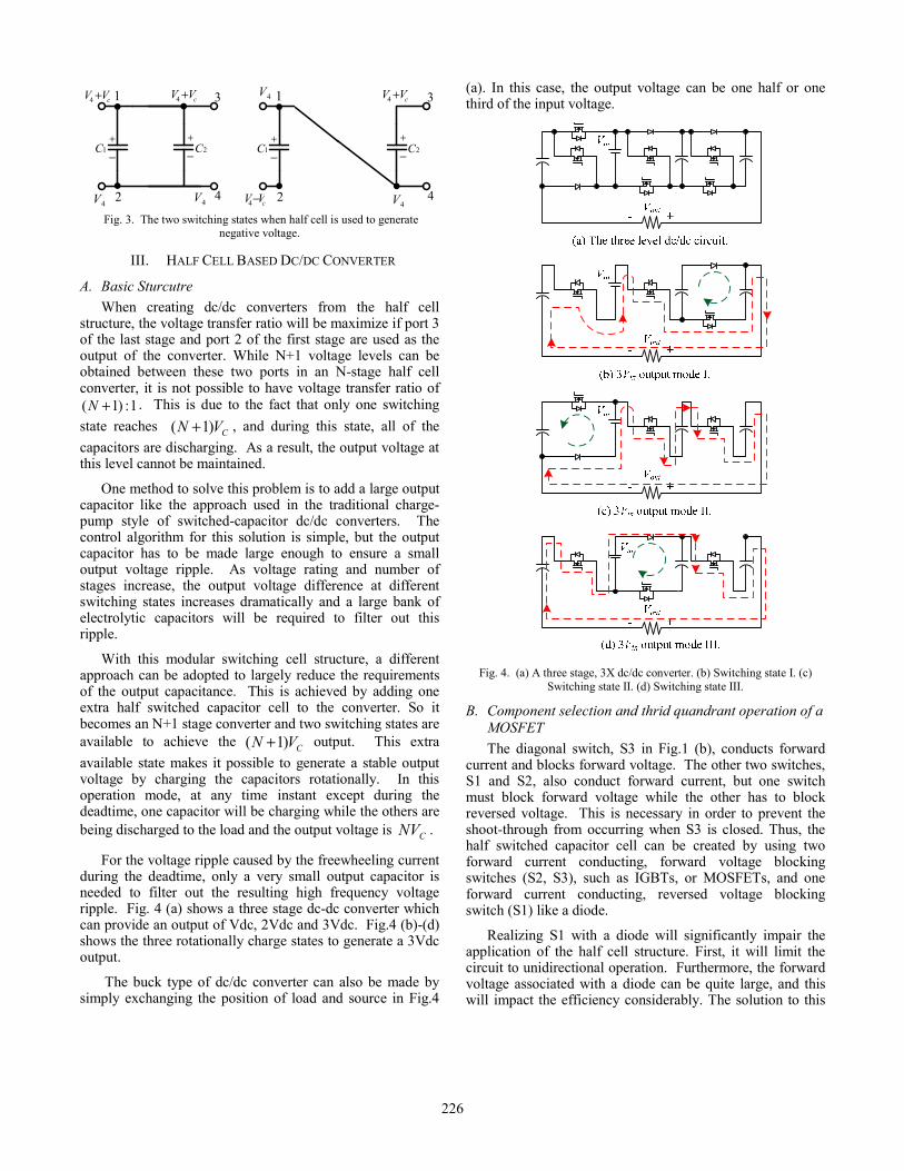
III. HALF CELL BASED DC/DC CONVERTER
A. Basic Sturcutre When creating dc/dc converters from the half cell
structure, the voltage transfer ratio will be maximize if port 3 of the last stage and port 2 of the first stage are used as the output of the converter. While N+1 voltage levels can be obtained between these two ports in an N-stage half cell converter, it is not possible to have voltage transfer ratio of
1:)1( +N . This is due to the fact that only one switching state reaches CVN )1( + , and during this state, all of the capacitors are discharging. As a result, the output voltage at this level cannot be maintained.
One method to solve this problem is to add a large output capacitor like the approach used in the traditional charge-pump style of switched-capacitor dc/dc converters. The control algorithm for this solution is simple, but the output capacitor has to be made large enough to ensure a small output voltage ripple. As voltage rating and number of stages increase, the output voltage difference at different switching states increases dramatically and a large bank of electrolytic capacitors will be required to filter out this ripple.
With this modular switching cell structure, a different approach can be adopted to largely reduce the requirements of the output capacitance. This is achieved by adding one extra half switched capacitor cell to the converter. So it becomes an N+1 stage converter and two switching states are available to achieve the CVN )1( + output. This extra available state makes it possible to generate a stable output voltage by charging the capacitors rotationally. In this operation mode, at any time instant except during the deadtime, one capacitor will be charging while the others are being discharged to the load and the output voltage is CNV .
For the voltage ripple caused by the freewheeling current during the deadtime, only a very small output capacitor is needed to filter out the resulting high frequency voltage ripple. Fig. 4 (a) shows a three stage dc-dc converter which can provide an output of Vdc, 2Vdc and 3Vdc. Fig.4 (b)-(d) shows the three rotationally charge states to generate a 3Vdc output.
The buck type of dc/dc converter can also be made by simply exchanging the position of load and source in Fig.4
(a). In this case, the output voltage can be one half or one third of the input voltage.
Fig. 4. (a) A three stage, 3X dc/dc converter. (b) Switching state I. (c)
Switching state II. (d) Switching state III.
B. Component selection and thrid quandrant operation of a MOSFET The diagonal switch, S3 in Fig.1 (b), conducts forward
current and blocks forward voltage. The other two switches, S1 and S2, also conduct forward current, but one switch must block forward voltage while the other has to block reversed voltage. This is necessary in order to prevent the shoot-through from occurring when S3 is closed. Thus, the half switched capacitor cell can be created by using two forward current conducting, forward voltage blocking switches (S2, S3), such as IGBTs, or MOSFETs, and one forward current conducting, reversed voltage blocking switch (S1) like a diode.
Realizing S1 with a diode will significantly impair the application of the half cell structure. First, it will limit the circuit to unidirectional operation. Furthermore, the forward voltage associated with a diode can be quite large, and this will impact the efficiency considerably. The solution to this
226
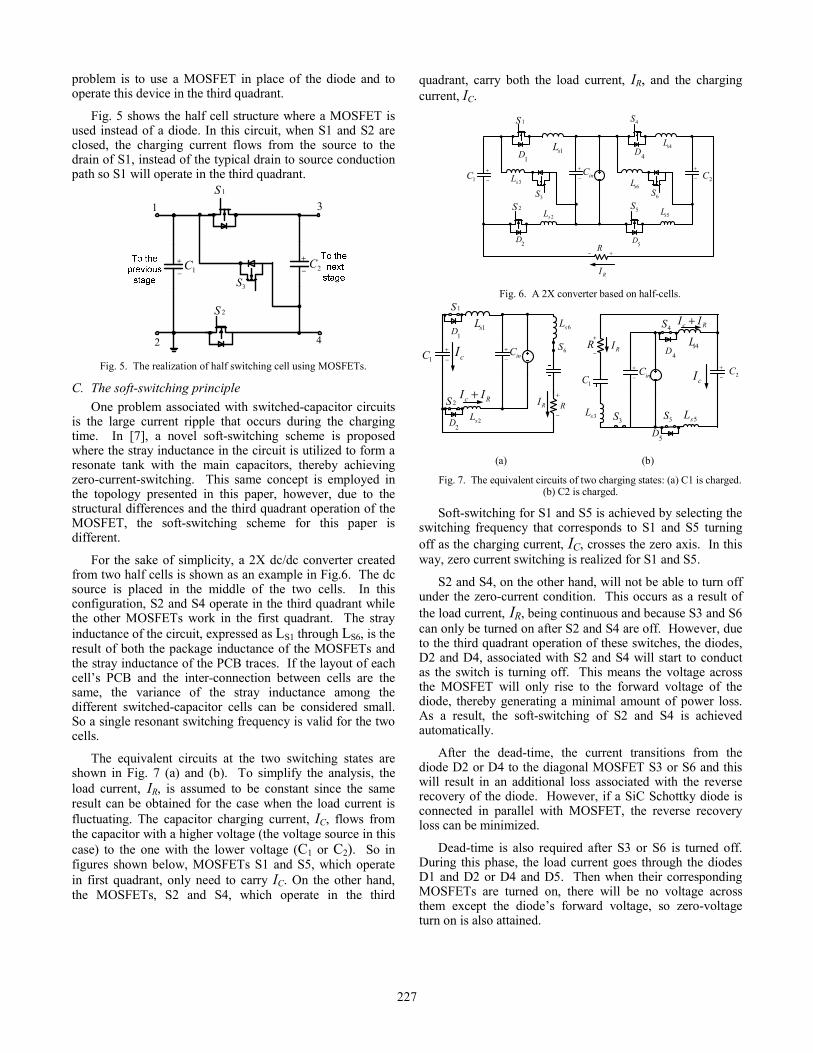
problem is to use a MOSFET in place of the diode and to operate this device in the third quadrant.
Fig. 5 shows the half cell structure where a MOSFET is used instead of a diode. In this circuit, when S1 and S2 are closed, the charging current flows from the source to the drain of S1, instead of the typical drain to source conduction path so S1 will operate in the third quadrant.
2S
3S1C+
−
+− 2C
1S1
2
3
4
Fig. 5. The realization of half switching cell using MOSFETs.
C. The soft-switching principle One problem associated with switched-capacitor circuits
is the large current ripple that occurs during the charging time. In [7], a novel soft-switching scheme is proposed where the stray inductance in the circuit is utilized to form a resonate tank with the main capacitors, thereby achieving zero-current-switching. This same concept is employed in the topology presented in this paper, however, due to the structural differences and the third quadrant operation of the MOSFET, the soft-switching scheme for this paper is different.
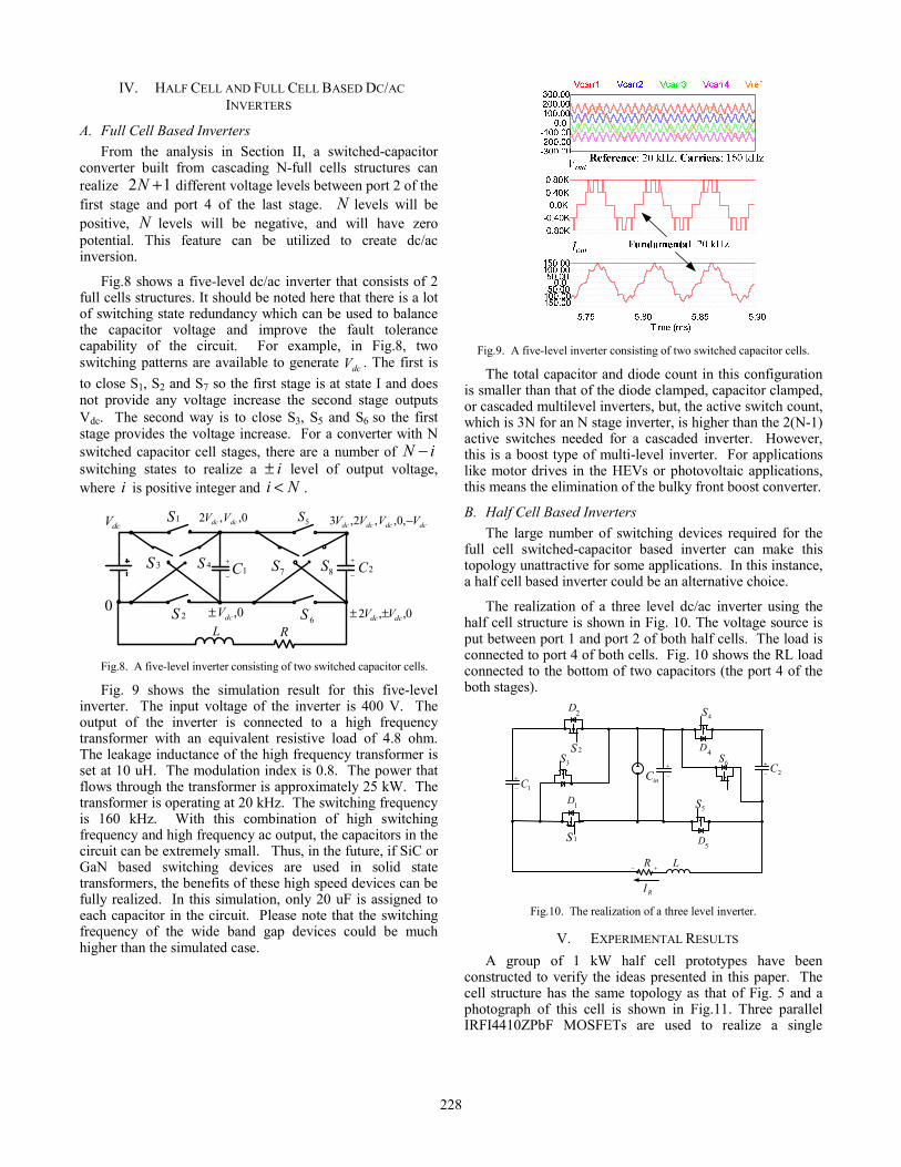
For the sake of simplicity, a 2X dc/dc converter created from two half cells is shown as an example in Fig.6. The dc source is placed in the middle of the two cells. In this configuration, S2 and S4 operate in the third quadrant while the other MOSFETs work in the first quadrant. The stray inductance of the circuit, expressed as LS1 through LS6, is the result of both the package inductance of the MOSFETs and the stray inductance of the PCB traces. If the layout of each cell’s PCB and the inter-connection between cells are the same, the variance of the stray inductance among the different switched-capacitor cells can be considered small. So a single resonant switching frequency is valid for the two cells.
The equivalent circuits at the two switching states are shown in Fig. 7 (a) and (b). To simplify the analysis, the load current, IR, is assumed to be constant since the same result can be obtained for the case when the load current is fluctuating. The capacitor charging current, IC, flows from the capacitor with a higher voltage (the voltage source in this case) to the one with the lower voltage (C1 or C2). So in figures shown below, MOSFETs S1 and S5, which operate in first quadrant, only need to carry IC. On the other hand, the MOSFETs, S2 and S4, which operate in the third
quadrant, carry both the load current, IR, and the charging current, IC.
2S3S
+
−
+
−
1S
+
−
1sL 4sL
6sL
4S
6S
5S5sL
1C 2CinC
R
3sL
2sL+−
RI
1D 4D
2D5D
Fig. 6. A 2X converter based on half-cells.
+
−
+−
1sL
1C inC
R
cI
Rc II +RI
1S
2S2sL
+
−
6sL
6S
2D
1D
3S
+
−
+−
4sL4S
1C 2CinC
R
3sL
RI+
−
cI
Rc II +
5S 5sL
5D
4D
(a) (b)
Fig. 7. The equivalent circuits of two charging states: (a) C1 is charged. (b) C2 is charged.
Soft-switching for S1 and S5 is achieved by selecting the switching frequency that corresponds to S1 and S5 turning off as the charging current, IC, crosses the zero axis. In this way, zero current switching is realized for S1 and S5.
S2 and S4, on the other hand, will not be able to turn off under the zero-current condition. This occurs as a result of the load current, IR, being continuous and because S3 and S6 can only be turned on after S2 and S4 are off. However, due to the third quadrant operation of these switches, the diodes, D2 and D4, associated with S2 and S4 will start to conduct as the switch is turning off. This means the voltage across the MOSFET will only rise to the forward voltage of the diode, thereby generating a minimal amount of power loss. As a result, the soft-switching of S2 and S4 is achieved automatically.
After the dead-time, the current transitions from the diode D2 or D4 to the diagonal MOSFET S3 or S6 and this will result in an additional loss associated with the reverse recovery of the diode. However, if a SiC Schottky diode is connected in parallel with MOSFET, the reverse recovery loss can be minimized.
Dead-time is also required after S3 or S6 is turned off. During this phase, the load current goes through the diodes D1 and D2 or D4 and D5. Then when their corresponding MOSFETs are turned on, there will be no voltage across them except the diode’s forward voltage, so zero-voltage turn on is also attained.
227
IV. HALF CELL AND FULL CELL BASED DC/AC INVERTERS
A. Full Cell Based Inverters From the analysis in Section II, a switched-capacitor
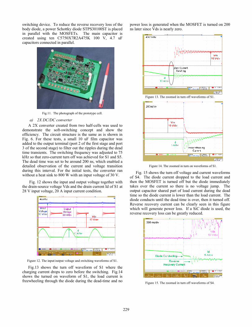
converter built from cascading N-full cells structures can realize 12 +N different voltage levels between port 2 of the first stage and port 4 of the last stage. N levels will be positive, N levels will be negative, and will have zero potential. This feature can be utilized to create dc/ac inversion.
Fig.8 shows a five-level dc/ac inverter that consists of 2 full cells structures. It should be noted here that there is a lot of switching state redundancy which can be used to balance the capacitor voltage and improve the fault tolerance capability of the circuit. For example, in Fig.8, two switching patterns are available to generate dcV . The first is to close S1, S2 and S7 so the first stage is at state I and does not provide any voltage increase the second stage outputs Vdc. The second way is to close S3, S5 and S6 so the first stage provides the voltage increase. For a converter with N switched capacitor cell stages, there are a number of iN −switching states to realize a i± level of output voltage, where i is positive integer and Ni < .
2C
dcV
0 0,dcV± 0,,2 dcdc VV ±±RL
6S
+
−
+
−
1S
3S 4S
0,,2 dcdc VV
1C
5Sdcdcdcdc VVVV −,0,,2,3
2S
7S 8S
Fig.8. A five-level inverter consisting of two switched capacitor cells.
Fig. 9 shows the simulation result for this five-level inverter. The input voltage of the inverter is 400 V. The output of the inverter is connected to a high frequency transformer with an equivalent resistive load of 4.8 ohm. The leakage inductance of the high frequency transformer is set at 10 uH. The modulation index is 0.8. The power that flows through the transformer is approximately 25 kW. The transformer is operating at 20 kHz. The switching frequency is 160 kHz. With this combination of high switching frequency and high frequency ac output, the capacitors in the circuit can be extremely small. Thus, in the future, if SiC or GaN based switching devices are used in solid state transformers, the benefits of these high speed devices can be fully realized. In this simulation, only 20 uF is assigned to each capacitor in the circuit. Please note that the switching frequency of the wide band gap devices could be much higher than the simulated case.
Fig.9. A five-level inverter consisting of two switched capacitor cells.
The total capacitor and diode count in this configuration is smaller than that of the diode clamped, capacitor clamped, or cascaded multilevel inverters, but, the active switch count, which is 3N for an N stage inverter, is higher than the 2(N-1) active switches needed for a cascaded inverter. However, this is a boost type of multi-level inverter. For applications like motor drives in the HEVs or photovoltaic applications, this means the elimination of the bulky front boost converter.
B. Half Cell Based Inverters The large number of switching devices required for the
full cell switched-capacitor based inverter can make this topology unattractive for some applications. In this instance, a half cell based inverter could be an alternative choice.
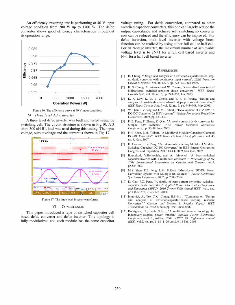
The realization of a three level dc/ac inverter using the half cell structure is shown in Fig. 10. The voltage source is put between port 1 and port 2 of both half cells. The load is connected to port 4 of both cells. Fig. 10 shows the RL load connected to the bottom of two capacitors (the port 4 of the both stages).
2S3S
+
−
1S
+
−
6S
5S
2CinC
R +−
RI
1D
4D
2D
5D
L
4S
+
−
1C
Fig.10. The realization of a three level inverter.
V. EXPERIMENTAL RESULTS A group of 1 kW half cell prototypes have been
constructed to verify the ideas presented in this paper. The cell structure has the same topology as that of Fig. 5 and a photograph of this cell is shown in Fig.11. Three parallel IRFI4410ZPbF MOSFETs are used to realize a single
228
switching device. To reduce the reverse recovery loss of the body diode, a power Schottky diode STPS30100ST is placed in parallel with the MOSFETs. The main capacitor is created using ten C5750X7R2A475K 100 V, 4.7 uF capacitors connected in parallel.
Fig.11. The photograph of the prototype cell.
a) 2X DC/DC converter A 2X converter created from two half-cells was used to
demonstrate the soft-switching concept and show the efficiency. The circuit structure is the same as is shown in Fig. 6. For these tests, a small 10 uF film capacitor was added to the output terminal (port 2 of the first stage and port 3 of the second stage) to filter out the ripples during the dead time transients. The switching frequency was adjusted to 75 kHz so that zero-current turn off was achieved for S1 and S5. The dead time was set to be around 200 ns, which enabled a detailed observation of the current and voltage transition during this interval. For the initial tests, the converter ran without a heat sink to 800 W with an input voltage of 30 V.
Fig. 12 shows the input and output voltage together with the drain-source voltage Vds and the drain current Id of S1 at 28 V input voltage, 20 A input current condition.
Figure 12. The input/output voltage and switching waveforms of S1.
Fig.13 shows the turn off waveform of S1 where the charging current drops to zero before the switching. Fig.14 shows the turned on waveform of S1, the load current is freewheeling through the diode during the dead-time and no
power loss is generated when the MOSFET is turned on 200 ns later since Vds is nearly zero.
Figure 13. The zoomed in turn off waveforms of S1.
Figure 14. The zoomed in turn on waveforms of S1.
Fig. 15 shows the turn off voltage and current waveforms of S4. The diode current dropped to the load current and then the MOSFET is turned off but the diode immediately takes over the current so there is no voltage jump. The output capacitor shared part of load current during the dead time so the diode current is lower than the load current. The diode conducts until the dead time is over, then it turned off. Reverse recovery current can be clearly seen in this figure which will generate power loss. If a SiC diode is used, the reverse recovery loss can be greatly reduced.
Figure 15. The zoomed in turn off waveforms of S4.
229
An efficiency sweeping test is performing at 40 V input voltage condition from 200 W up to 1700 W. The dc/dc converter shows good efficiency characteristics throughout its operation range.
Figure 16. The efficiency curve at 40 V input condition. b) Three level dc/ac inverter
A three level dc/ac inverter was built and tested using the switching cell. The circuit structure is shown in Fig.10. A 3 ohm, 300 uH RL load was used during this testing. The input voltage, output voltage and the current is shown in Fig. 17.
Figure 17. The three level inverter waveforms.
VI. CONCULUSION This paper introduced a type of switched capacitor cell
based dc/dc converter and dc/ac inverter. This topology is fully modularized and each module has the same capacitor
voltage rating. For dc/dc conversion, compared to other switched capacitor converters, this one can largely reduce the output capacitance and achieve soft switching so converter cost can be reduced and the efficiency can be improved. For dc/ac inversion, multi-level inverter with voltage boost function can be realized by using either full cell or half cell. For an N-stage inverter, the maximum number of achievable voltage level is to 2N+1 for a full cell based inverter and N+1 for a half cell based inverter.
REFERENCES [1] H. Chung, “Design and analysis of a switched-capacitor-based step-
up dc/dc converter with continuous input current”, IEEE Trans. on Circuit & Systems, vol. 46, no. 6, pp. 722~730, Jun 1999.
[2] H. S. Chung, A. Ioinovici and W. Cheung, “Generalized structure of bidirectional switched-capacitor dc/dc converters,” IEEE Trans. Circuits Syst., vol. 50, no. 6, pp. 743–753, Jun. 2003.
[3] K. K. Law, K. W. E. Cheng, and Y. P. B. Yeung, “Design and analysis of switched-capacitor-based step-up resonant converters,” IEEE Trans.Circuits Syst. I, vol. 52, no. 5, pp. 943–948, May 2005.
[4] W. Qian, F.Z.Peng and L.M. Tolbert,; “Development of a 55 kW 3X DC-DC Converter for HEV systems”, Vehicle Power and Propulsion Conference, 2009, pp. 433-439.
[5] F. Z. Peng, F. Zhang, Z. Qian, "A novel compact dc-dc converter for Simp1e 42V systems," IEEE Power lectronics Specialists Conference, pp. 33-38, June 2003.
[6] F.H. Khan, L.M. Tolbert, “A Multilevel Modular Capacitor-Clamped DC–DC Converter”, IEEE Trans. On Industrial Applications, vol. 43, no. 6, Nov. 2007.
[7] D. Cao and F. Z. Peng, "Zero-Current-Switching Multilevel Modular Switched-Capacitor DC-DC Converter," in IEEE Energy Conversion Congress and Exposition, 2009. ECCE 2009. San Jose, 2009.
[8] B.Axelrod, Y.Berkovich, and A. Ioinovici, “A boost-switched capacitor-inverter with a multilevel waveform ”, Proceedings of the 2004 International Symposium on Circuits and Systems, vol.5, pp.884-887.
[9] M.S. Shen, F.Z. Peng, L.M. Tolbert, “Multi-Level DC/DC Power Conversion System with Multiple DC Sources ”, Power Electronics Specialists Conference, 2007,pp. 2008-2014.
[10] D. Cao; F.Z. Peng, "A family of zero current switching switched-capacitor dc-dc converters," Applied Power Electronics Conference and Exposition (APEC), 2010 Twenty-Fifth Annual IEEE , vol., no., pp.1365-1372, 21-25 Feb. 2010.
[11] Ioinovici, A.; Tse, C.K.; Chung, H.S.-H.; , "Comments on "Design and analysis of switched-capacitor-based step-up resonant Converters"," Circuits and Systems I: Regular Papers, IEEE Transactions on , vol.53, no.6, pp.1403, June 2006
[12] Rodriguez, J.I.; Leeb, S.B.; , "A multilevel inverter topology for inductively-coupled power transfer," Applied Power Electronics Conference and Exposition, 2003. APEC '03. Eighteenth Annual IEEE , vol.2, no., pp. 1118- 1126 vol.2, 9-13 Feb. 2003
0.955
0.96
0.965
0.97
0.975
0.98
0.985
0 500 1000 1500 2000
Effic
ienc
y
Operation Power (W)
230