Embed Size (px)
Citation preview

ENG241/ Lab #2 1
ENG2410 Digital Design
LAB #2 Xilinix ISE Foundation Tools
Schematic Capture
“A Tutorial”
ENG241/ Lab #2 2
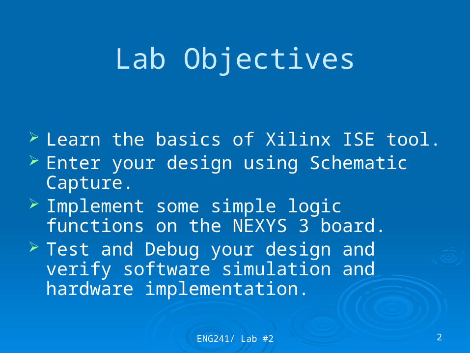
Lab Objectives
Learn the basics of Xilinx ISE tool. Enter your design using Schematic Capture. Implement some simple logic functions on the
NEXYS 3 board. Test and Debug your design and verify software
simulation and hardware implementation.
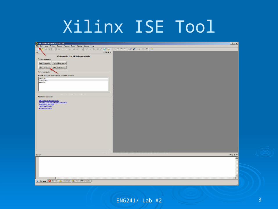
Xilinx ISE Tool
ENG241/ Lab #2 3

ENG241/ Lab #2 4
Schematic Capture
Sample circuit entered using Schematic Capture. Note that this is not the circuit you will be building
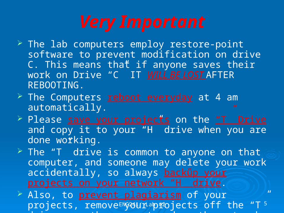
Very Important
ENG241/ Lab #2 5
The lab computers employ restore-point software to prevent modification on drive C. This means that if anyone saves their work on Drive “C” IT WILL BE LOST AFTER REBOOTING.
The Computers reboot everyday at 4 am automatically. Please save your projects on the “T” Drive and copy it to
your “H” drive when you are done working. The “T” drive is common to anyone on that computer,
and someone may delete your work accidentally, so always backup your projects on your network “H” drive.
Also, to prevent plagiarism of your projects, remove your projects off the “T” drive once they are stored on the network drive.
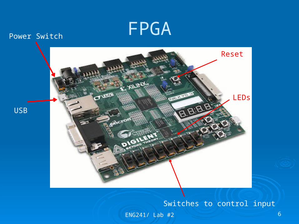
FPGA
ENG241/ Lab #2 6
USB
Reset
Switches to control input
LEDs
Power Switch

FPGA
ENG241/ Lab #2 7
A B C D Z
0 0 0 0 0 0 0 0 1 1 0 0 1 0 1 0 0 1 1 1 0 1 0 0 0 0 1 0 1 1 0 1 1 0 1 0 1 1 1 1 1 0 0 0 0 1 0 0 1 1 1 0 1 0 1 1 0 1 1 1 1 1 0 0 0 1 1 0 1 0 1 1 1 0 0
LUTLUT
ABCD
Z
LUT implementation
ENG241/ Lab #2 8
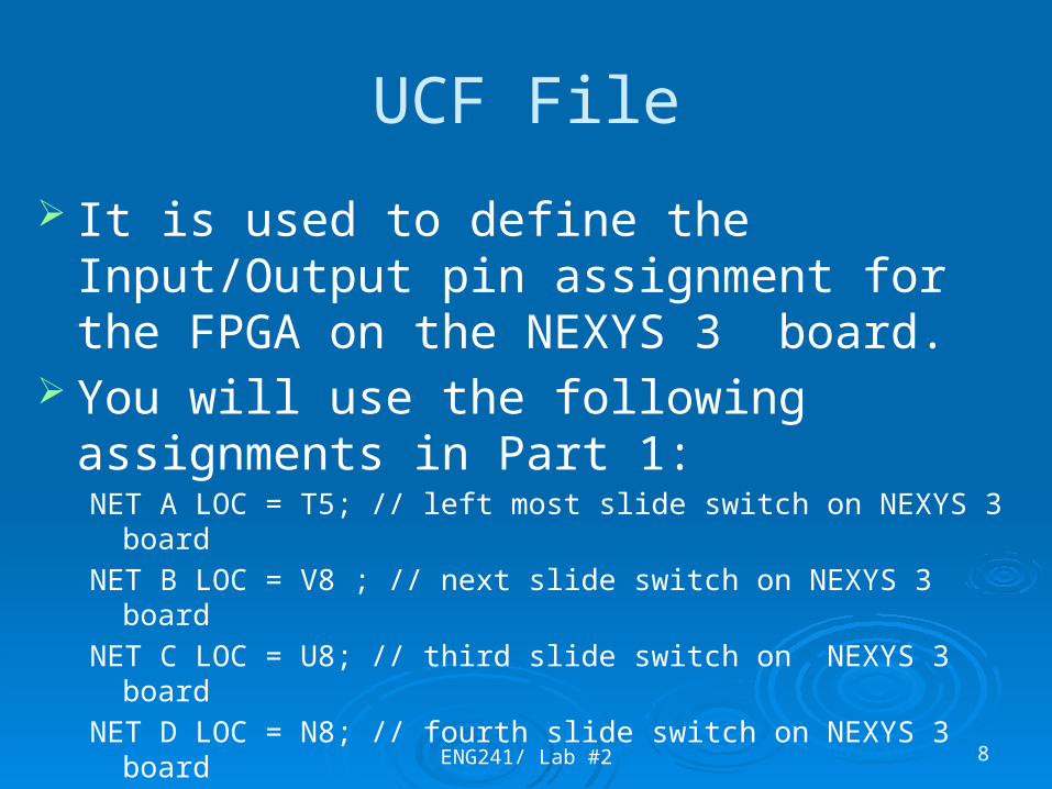
UCF File
It is used to define the Input/Output pin assignment for the FPGA on the NEXYS 3 board.
You will use the following assignments in Part 1:NET A LOC = T5; // left most slide switch on NEXYS 3 boardNET B LOC = V8 ; // next slide switch on NEXYS 3 boardNET C LOC = U8; // third slide switch on NEXYS 3 boardNET D LOC = N8; // fourth slide switch on NEXYS 3 boardNET E LOC = T11; // left most LED on NEXYS 3 board

Digilent Adept Tool
ENG241/ Lab #2 9
The Digilent Adept Tool is used to:1. Test the FPGA
board.2. Program the
FPGA board.Check Appendix A in the Tutorial

Behavioral Simulation
ENG241/ Lab #2 10

Test Bench
ENG241/ Lab #2 11
BEGIN
A_tb <= '0'; -- apply input combination 00 and check outputs
B_tb <= '0'; wait for period;
assert ((S_tb = '0') and (C_tb = '0'))
report "test failed for input combination 00" severity error;
...
…

ENG241/ Lab #2 12
Part 1 Implement the Following function:
Derive its truth table and Circuit diagram. Implement the design using Xilinx ISE
Schematic Capture tool Test and Debug your Circuit. Use the UCF file provided to you in the
hand-out.
))(( DACCBAE
ENG241/ Lab #2 13
Part 2 In this part you will use Xilinx ISE
schematic capture tool again to enter your design.
The circuit has two inputs (X and Y) and one output (F). The function F is true when X and Y are different, and false when they are the same.
Derive the truth table, and give an expression for F. Assume X is MSD
Draw the circuit diagram.

ENG241/ Lab #2 14
Cont … Part 2 Enter the design using Schematic
Capture. Simulate your design. Go Through the implementation process
until you download your design on the NEXYS 3 board.
Create the UCF file for this circuit on your own.
Verify your Implementation.

Academic Misconduct
Reports and demos are submitted as a group, but it is a SINGLE group effort
You may talk with other groups but sharing codes or reports is NOT ALLOWED
Copying reports from previous years is also NOT ALLOWED
If we find copying we are REQUIRED to report it