Embed Size (px)
Citation preview
ESCUELA TÉCNICA SUPERIOR DE INGENIERÍA (ICAI)
INGENIERO INDUSTRIAL
JAVACORES
Autor: Cristina León Heredia
Director: Ernest M. Kim
Madrid Junio 2012
JavaCores !
2!
JAVACORES
Autor: Cristina Leon Heredia
Director: Ernest M. Kim
Entidad Colaboradora: JavaCores
Resumen del Proyecto
En la actualidad el mercado de los teléfonos móviles, en concreto de smartphones y
tabletas, se encuentra creciendo a un ritmo exponencial aumentando así mismo la
demanda por estos productos electrónicos cada vez más avanzados. A su vez, es
necesario que se diseñen plataformas de desarrollo capaces de integrar los nuevos
productos de hardware y software de estos dispositivos móviles. Por este motivo la
compañía JavaCores desarrolló a finales de los años 90 un nuevo microprocesador, el
Xpresso Core (XC-110). La principal característica, y a si mismo novedad, del XC-110
es que este procesador ejecuta Java™ directamente en hardware sin necesitar una JVM
(Java Virtual Machine). Para evidenciar las magnificas cualidades del XC-110, las
cuales incluyen menor consumo de energía y mayor rapidez de proceso de datos,
JavaCores construyó en el 2002 la plataforma de demostración “Slim Board”. Sin
embargo, debido a la quiebra de la empresa, JavaCores Inc. no pudo lanzar al mercado el
novedoso microprocesador XC-110. A día de hoy, JavaCores ha retomado su proyecto y
busca la manera de renovar la antigua plataforma “Slim Board”. Este proyecto ha
consistido pues en el diseño, desarrollo y construcción de una nueva plataforma de
demostración llamada “Panda Xpresso”. Además de poder demostrar las capacidades del
JavaCores !
3!
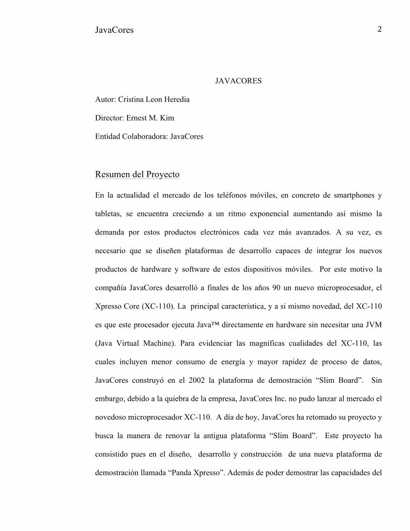
XC-110, la Panda Xpresso tiene múltiples utilidades como por ejemplo conversor
analógico-digital o verificación de datos y operaciones. JavaCores especificó que la
nueva plataforma funcionase como una tarjeta mezzanine de la ya existente PandaBoard.
De esta manera, la plataforma PandaBoard sería el procesador central del sistema,
incorporando ventajas tal y como WLAN, Bluetooth™, ranura para Tarjeta SD, o ranura
de expansión para cámara.
Figure 1: PandaBoard Mother Card
Además, la Panda Xpresso es puntera en cuanto a la tecnología que lleva implementada,
ya que contiene el Spartan 6 LX150T FPGA de Xilinx, el FPGA más avanzado del
mercado. Otros de los requisitos que JavaCores ha demandado para este proyecto son la
disminución en tamaño de la plataforma así como su versatilidad, los cuales han sido
llevados a cabo gracias a la incorporación de nuevas tecnologías. Al utilizar nuevos y
avanzados módulos de memoria, además del anteriormente nombrado FPGA, el tamaño
de la tabla ha disminuido notablemente.
Durante el curso del proyecto se han llevado a cabo cuatro tareas principales. La primera
etapa del proyecto ha sido realmente creativa, ha consistido en buscar diferentes
JavaCores !
4!
aproximaciones que cumpliesen los requisitos de JavaCores. Seguidamente, el trabajo
de selección de componentes. A continuación tuvo lugar el diseño esquemático y el
bosquejo y trazado de la Panda Xpresso utilizando el programa de diseño Proteus.
Finalmente, una vez que la Panda Xpresso fue manufacturada, se diseño un código
programable para verificar y demostrar su correcto funcionamiento.
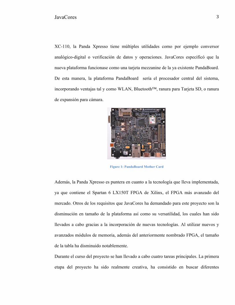
A la hora de demostrar el funcionamiento conjunto de la PandaBoard y la Panda
Xpresso surgió un contratiempo debido a que la licencia de estudiante del software
obtenido (Xilinx 13.4) no se correspondía con la versión requerida para el FPGA
Spartan 6 LX150T. No obstante, la recreación del kit de evaluación Spartan 3 (en lugar
del Spartan 6 FPGA) junto a la PandaBoard fue realmente satisfactoria.
Figure 2: Spartan 3 EVK and PandaBoard System
Figure 3: Screenshot Testing System
JavaCores !
5!
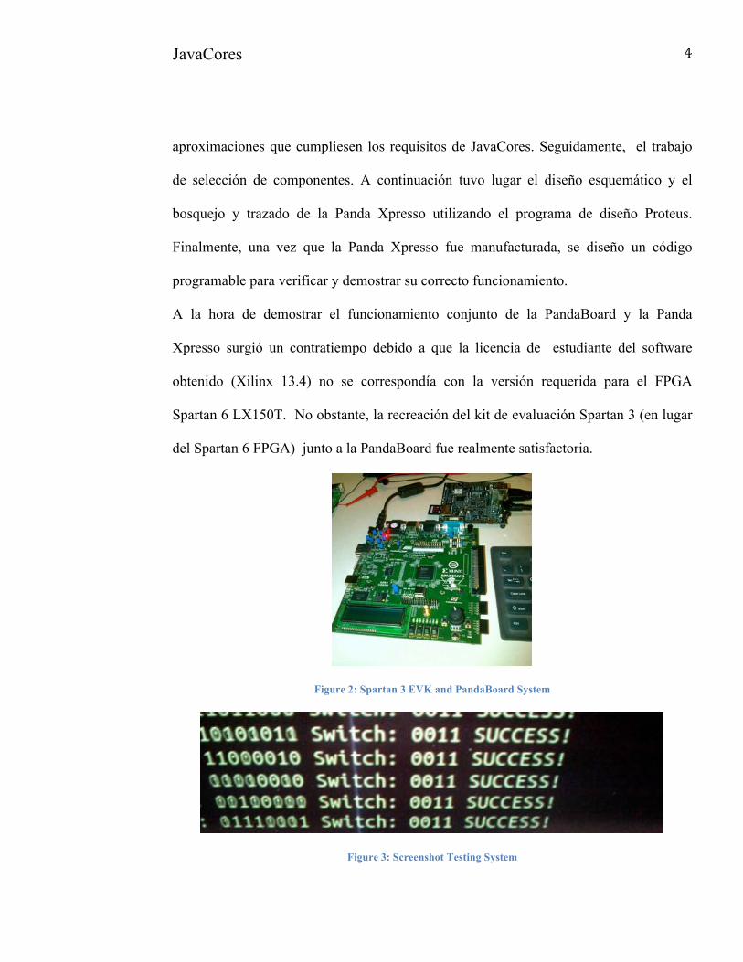
Asimismo, queda demostrado el correcto funcionamiento de la Panda Xpresso pues
además de haber comprobado las lecturas de todos los voltajes y las fuentes de tensión,
el software de Xilinx reconoció tanto el FPGA como la plataforma de memoria Flash.
Figure 4: Panda Xpresso
Figure 5: FPGA and Flash Memory Caption
En resumen, la interconexión entre el kit de evaluación Spartan 3 y la PandaBoard
funciona de la misma manera que la Panda Xpresso con la PandaBoard. El método de
JavaCores !
6!
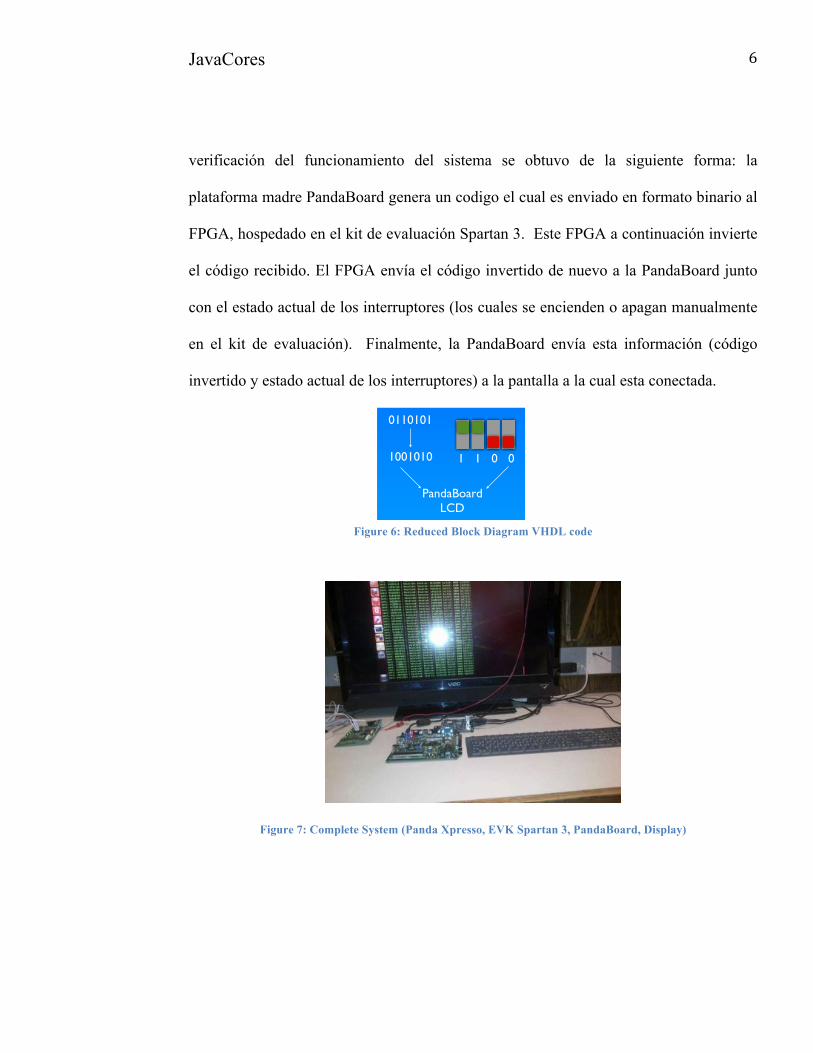
verificación del funcionamiento del sistema se obtuvo de la siguiente forma: la
plataforma madre PandaBoard genera un codigo el cual es enviado en formato binario al
FPGA, hospedado en el kit de evaluación Spartan 3. Este FPGA a continuación invierte
el código recibido. El FPGA envía el código invertido de nuevo a la PandaBoard junto
con el estado actual de los interruptores (los cuales se encienden o apagan manualmente
en el kit de evaluación). Finalmente, la PandaBoard envía esta información (código
invertido y estado actual de los interruptores) a la pantalla a la cual esta conectada.
Figure 6: Reduced Block Diagram VHDL code
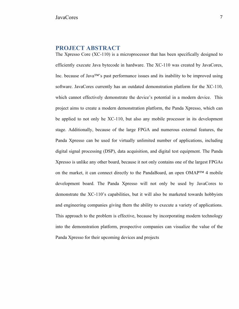
Figure 7: Complete System (Panda Xpresso, EVK Spartan 3, PandaBoard, Display)
Software Overview
© 2012 JavaCores, Inc
Send binary byte from
PandaBoard to FPGA
PandaBoard generates random
byte
0110101
1001010 1 1 0 0
PandaBoardLCD
Invert binary byte using FPGA
Obtain switch statefrom FPGA
Sent inverted binary byte
back to PandaBoard
Send switch state back to PandaBoard
Display receivedbyte and
switch state
JavaCores !
7!
PROJECT ABSTRACT The Xpresso Core (XC-110) is a microprocessor that has been specifically designed to
efficiently execute Java bytecode in hardware. The XC-110 was created by JavaCores,
Inc. because of Java™’s past performance issues and its inability to be improved using
software. JavaCores currently has an outdated demonstration platform for the XC-110,
which cannot effectively demonstrate the device’s potential in a modern device. This
project aims to create a modern demonstration platform, the Panda Xpresso, which can
be applied to not only he XC-110, but also any mobile processor in its development
stage. Additionally, because of the large FPGA and numerous external features, the
Panda Xpresso can be used for virtually unlimited number of applications, including
digital signal processing (DSP), data acquisition, and digital test equipment. The Panda
Xpresso is unlike any other board, because it not only contains one of the largest FPGAs
on the market, it can connect directly to the PandaBoard, an open OMAP™ 4 mobile
development board. The Panda Xpresso will not only be used by JavaCores to
demonstrate the XC-110’s capabilities, but it will also be marketed towards hobbyists
and engineering companies giving them the ability to execute a variety of applications.
This approach to the problem is effective, because by incorporating modern technology
into the demonstration platform, prospective companies can visualize the value of the
Panda Xpresso for their upcoming devices and projects
JavaCores !
8!
INDEX PROJECT ABSTRACT .................................................................................................. 7!WORK STATEMENT .................................................................................................. 11!CONTEXT!................................................................................................................................................................!11!1.1. BACKGROUND OF NEED!......................................................................................................................!11!
1.1.2 CUSTOMER NEED STATEMENT!......................................................................................................!12!1.2 PREVIOUS WORKS AND STUDIES!....................................................................................................!12!
1.2.1 PRIOR WORK!..............................................................................................................................................!12!1.2.2 RELATED TECHNOLOGY!....................................................................................................................!13!
1.3 PATENTS!..........................................................................................................................................................!15!1.4 PROBLEM DEFINITION!............................................................................................................................!15!
1.4.1 CUSTOMER REQUIREMENTS!...........................................................................................................!16!PHYSICAL REQUIREMENTS!..........................................................................................................................!16!FUNCTIONAL REQUIREMENTS!..................................................................................................................!17!1.4.2 ASSUMPTIONS!...........................................................................................................................................!17!1.4.3 CONSTRAINTS!...........................................................................................................................................!18!
1.5 CONCEPT DEVELOPMENT!....................................................................................................................!19!OVERVIEW!.............................................................................................................................................................!19!
1.5.1 CREATIVE STRATEGIES!.......................................................................................................................!19!1.5.2 SYNTHESIS OF OVERALL CONCEPTS!..........................................................................................!20!1.5.3 ANALYSIS OF THE OVERALL CONCEPTS!..................................................................................!24!1.5.3 FINAL EVALUATION!..............................................................................................................................!28!
1.6 DESIGN SPECIFICATIONS!......................................................................................................................!31!1.6.1 BLOCK DIAGRAMS!.................................................................................................................................!31!1.6.2 GOVERNING PRINCIPLES!..................................................................................................................!31!
1.7 SYSTEM ANALYSIS AND DESIGN!....................................................................................................!38!1.7.1 SOFTWARE!..................................................................................................................................................!38!1.7.2 HARDWARE!.................................................................................................................................................!38!1.7.3 SUBSYSTEM ANALYSIS AND DESIGN!...........................................................................................!39!
1.8 CALCULATIONS!..........................................................................................................................................!41!1.8.1 RESISTORS’ VALUES!..............................................................................................................................!41!1.8.2 DDR3 TRACE LENGTHS!.......................................................................................................................!42!
1.9 ECONOMIC RESEARCH!...........................................................................................................................!44!1.9.1 VIABILITY!.....................................................................................................................................................!44!1.9.2 ECONOMIC INTEREST!..........................................................................................................................!45!
1.10.1 APPENDIX I: Panda Xpresso Block Diagram!................................................................................!47!1.10.2 APPENDIX II: Vendor information!..................................................................................................!49!A- Accutrace Incorporated!.................................................................................................................................!49!B- KYOCERA Display Corporation!...............................................................................................................!49!C- QSIC!.....................................................................................................................................................................!50!1.10.3 APPENDIX III: PATENTS!...................................................................................................................!51!1.10.4 APPENDIX IV: COMMONLY USED ACRONYMS!...................................................................!52!1.10.5 APPENDIX V: SOFTWARE CODE!.................................................................................................!53!
PLANES ......................................................................................................................... 68!2.1 LIST OF PLANES!..........................................................................................................................................!68!

JavaCores !
9!
A- Schematic!............................................................................................................................................................!68!B- Layout!...................................................................................................................................................................!68!
2.2 PLANES!.............................................................................................................................................................!69!A- Schematic!............................................................................................................................................................!69!B- Layout!...................................................................................................................................................................!82!
PROJECT PLAN ........................................................................................................... 90!3.1!GENERAL!AND!ECONOMIC!PROJECT!PLAN!.......................................................................................!90!3.2 TECHNICAL AND PARTICULAR PROJECT PLAN!.....................................................................!91!
3.2.1 FABRICATION!............................................................................................................................................!91!3.2.2 TESTING!........................................................................................................................................................!91!3.2.3 PROJECT DELIVERABLES!..................................................................................................................!93!3.2.4 FINAL DELIVERABLE!............................................................................................................................!94!3.2.5 SCHEDULE!..................................................................................................................................................!95!
BUDGET ........................................................................................................................ 96!4.1 BILL OF MATERIALS!................................................................................................................................!96!4.2 GENERAL BUDGET!.................................................................................................................................!100! LIST OF FIGURES Figure 1: PandaBoard Mother Card ................................................................................... 3 Figure 2: Spartan 3 EVK and PandaBoard System ........................................................... 4 Figure 3: Screenshot Testing System ................................................................................ 4 Figure 4: Panda Xpresso .................................................................................................... 5 Figure 5: FPGA and Flash Memory Caption .................................................................... 5 Figure 6: Reduced Block Diagram VHDL code ............................................................... 6 Figure 7: Complete System (Panda Xpresso, EVK Spartan 3, PandaBoard, Display) ..... 6 Figure 8: Slim Board Schematic ...................................................................................... 20 Figure 9: New Demonstration Kit Preliminary Schematic .............................................. 21 Figure 10: Smartphone Integration Schematic ................................................................ 22 Figure 11: PC Integration Schematic ............................................................................... 23 Figure 12: Slim Board ..................................................................................................... 24 Figure 13: Smartphone Integration Diagram ................................................................... 27 Figure 14: Panda Xpresso Reduced Block Diagram ....................................................... 34 Figure 15: Panda Xpresso Display Block Diagram ......................................................... 34 Figure 16: Panda Xpresso USB/ RS-232/ JATG Block Diagram ................................... 35 Figure 17: Panda Xpresso DAC's & ADC's Block Diagram ........................................... 36 Figure 18: Panda Xpresso Memory Block Diagram ....................................................... 36 Figure 19: Panda Xpresso Extras Block Diagram ........................................................... 37 Figure 20: Basic System Block Diagram ........................................................................ 47 Figure 21: Final System Block Diagram ......................................................................... 48 Figure 22: PandaBoard and Spartan 3A Setup ................................................................ 92 Figure 23: Software Block Diagram ................................................................................ 93
JavaCores !
10!
LIST OF TABLES Table 1: Final Decision Matrix!..........................................................................................................!30!Table 2: Numerical Results of Resistor's Values!.........................................................................!42!Table 3: DDR3 Trace Lengths!...........................................................................................................!44!Table 4: General Budget!.....................................................................................................................!100!
!!!!!!!!!!!!!!!!!!!!!
JavaCores !
11!
WORK STATEMENT CONTEXT
1.1. BACKGROUND OF NEED JavaCores is in need of a demonstration platform that will feature the Java™- processing
capabilities of the XC-110 processor. JavaCores currently has an outdated demonstration
platform that includes a low-resolution, non-touch- sensitive LCD, a memory of 8MB of
RAM, several small FPGAs, and is large in size. Due to these constraints, the board is
not an adequate representation of a modern mobile device. JavaCores has requested that
the new mobile demonstration platform be based on an existing mobile development kit
to act as the host processor, such as the TI™ PandaBoard.
The PandaBoard is a low-cost open development board based on Texas Instruments’
OMAP™4 processor. The PandaBoard is geared towards the development of
smartphones and other mobile devices. The PandaBoard includes features common to
modern mobile devices, such as WLAN, Bluetooth™, SD Card slot, camera expansion
connector, and 1GB of DDR2 RAM. The PandaBoard lacks an FPGA, which can be
very useful when developing mobile processors. Although the PandaBoard is great for
mobile software development, it lacks the ability for a developer to implement his/her
own hardware design. Additionally, the PandaBoard cannot easily connect with many
external devices, which greatly limits its functionality to the mobile software
development sector.
With the exponentially growing market for faster and more efficient smartphones, the
demand for a mobile hardware/software development platform is increasing
JavaCores !
12!
significantly. Because mobile device processors and other components are constantly
changing, there is a need for a flexible platform that can integrate new hardware and
software designs.
1.1.2 CUSTOMER NEED STATEMENT JavaCores has requested a device to demonstrate the efficiency of the XC-110 processor,
which can emphasize its fast performance and low power consumption. JavaCores has
requested that only the hardware be developed, as the software must be developed by a
team of software and processor architecture engineers. Additionally, JavaCores has
requested that the demonstration platform use the PandaBoard as a host-processing
platform, which will allow the demonstration platform to be marketable in and of itself.
This platform must incorporate modern technology, in order to represent a modern
mobile device. The updated demonstration platform will be used by JavaCores to
express to prospective companies how the XC-110 can be used to benefit their product
line, as well as for marketing the board it self. For this purpose, the project involves the
design, construction and implementation of a mezzanine card named Panda Xpresso.
1.2 PREVIOUS WORKS AND STUDIES
1.2.1 PRIOR WORK Unlike other Java™-capable processors, this processor executes Java™ directly in
hardware and does not require a Java Virtual Machine (JVM). There are plenty of other
options when it comes to microprocessors, but the Xpresso core is designed specifically
for cell phones and tablets which run Java™, and enhance the performance of essentially
JavaCores !
13!
everything written in Java™ code. Because Java™ is frequently inconsistent, due to the
numerous versions and the need to update the software constantly; the XC-110 has been
specifically designed to use Java™ standards to reduce errors associated with these
inconsistencies. This processor will have the ability to demonstrate the features of
Java™ while proving to the technological society that there is a way to optimize Java™.
The project is directly adopted from JavaCores, and thus, it involves a deep
understanding and interpreting of the large amount of work that has already been
previously completed. The microprocessor presently rests on a Printed Circuit Board
(PCB) platform that uses four Field Programmable Gate Arrays (FPGAs), a Liquid
Crystal Display (LCD), and numerous external interfaces. However, most of the
technology within this PCB is out of date, and therefore it is far from being appealing to
most major companies. The XC-110 was designed by JavaCores several years ago, but
unfortunately the company ran out of resources before they were able to finalize and
market their processor. There is Very High Speed Integrated Circuit Hardware
Description Language (VHDL) code that has been developed by the software team at
JavaCores, that at one time (using older versions of Xilinx) would synthesize onto the
previous platform. However, this old demonstration platform must be rebuilt before this
processor will be deemed marketable.
1.2.2 RELATED TECHNOLOGY There is a design similar to the Panda Xpresso, called the PandaDAQ, developed by
Mark Haun. The PandaDAQ is optimized for data acquisition and uses a significantly
smaller FPGA that would not be suitable for processor development. Mark Haun has
JavaCores !
14!
developed a way for an FPGA to be programmed through the PandaBoard’s expansion
header. The PandaDAQ is a reference design and is not intended for production and sale.
There are three other FPGA daughter card designs for the PandaBoard, however these
projects have not made any significant developments in the past year.
The XC-110 chip is not the only Java™ processor currently in development.
a) When Java™ was first developed by Sun Microsystems, the company developed
a Java™ processor called picoJava (Wikipedia), but never publicly released a
production version of the product. Fujitsu further developed picoJava, but only
released a development kit for the processor.
b) ARM Holdings currently makes a processor called the ARM926EJ-S (ARM
Ltd), which is essentially an ARM9 processor with the capability to execute
Java™ instructions in hardware. The ARM processor is able to do this through a
technology called Jazelle, which is very similar to the XC-110 chip. However,
this accelerator has many disadvantages. For instance it does not implement
acceleration on all the instructions, it does not have a very integrated strategy in
terms of integration within a product and it requires context switch to get in and
out.
c) Temple Computing Labs is currently developing a Java™ processor as well
(Temple Computing). However, this company is still in the early development
stages, while the Xpresso chip simply needs to be demonstrated and properly
JavaCores !
15!
marketed. Additionally, unlike the XC-110, Temple’s processor is not geared
towards and optimized for mobile devices.
d) Ajile Systems currently produces a Java™ Microprocessor similar to the Xpresso
chip. Their product, however, is only sold on a PCB with specific interface
components. The Ajile Systems processor has not been tailored to the needs of
mobile device manufacturers.
e) Another company that sells Java™ processors is Imsys. All of Imsys’ products
are geared toward high-speed, efficient networking applications, not mobile
devices (Imsys AB).
f) There is also a processor called the Java™ Optimized Processor (JOP)
(Schoeberl, 2008). Unlike the XC-110, which is designed to be one of the cores
within a multi-core processor of a mobile device, the JOP is intended for use in
experimental applications, specifically FPGA setups.
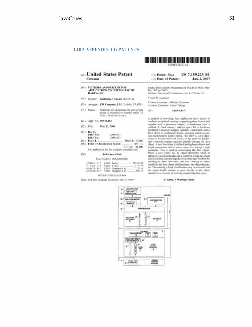
1.3 PATENTS The following presents the patent that has been granted to JavaCores for the XC-110
processor. The patent, Methods and Systems for Applications to Interact with Hardware,
Patent No. 7,1259,223, was granted on Jan 2, 2007. The patent is unique in that the XC-
110 Java™ processor can share memory and a display with the host processor. This
method allows for faster application processing, even when compared to competing
Java™ processors. This can be viewed in Appendix III.
1.4 PROBLEM DEFINITION
JavaCores !
16!
As mobile devices become increasingly common, the demand for smaller, lighter, faster
devices with longer battery life is rapidly increasing. A device that incorporates an
Xpresso Core will operate faster and consume less power. However, at the XC-110’s
current state it is not marketable because its features cannot be properly and thoroughly
demonstrated. In order to demonstrate the Xpresso chip’s unique advantages, the chip
needs to be placed in a simulated device platform. The platform must attach to the
PandaBoard and be capable of performing in a wide range of applications. Using a
PandaBoard is highly helpful in order to minimize error when rebuilding the platform as
the work is reduced to the creation of the daughter card, which only houses the FPGA
and extra peripherals. Therefore, it has not been necessary to build a “mother” board in
line with the PandaBoard from scratch.
The project enhances the experience and understanding of the engineering behind
modern tablets and smartphones. The future users of the versatile Panda Xpresso will
take advantage of the fast XC-110 Java™ microprocessor and the rest of its multiple
uses, which will highly improve the performance of cellular devices and tablets.
1.4.1 CUSTOMER REQUIREMENTS
PHYSICAL REQUIREMENTS
1. Device must be portable (H)
a. No larger than a standard tablet (excluding thickness) (H)
b. Must weigh no more than 3 pounds (L)
c. 8 layers or less PCB stack up (M)
JavaCores !
17!
2. LCD size of at least 3 in with the possibility of touch sensitive capabilities (M)
3. Device will be powered through the PandaBoard’s expansion header (H)
4. Device should mount directly to the PandaBoard (H)
5. Platform components (excluding display, FPGA, and PandaBoard) should be less
than $200 (M)
6. Manufacturing cost of five identical PCBs should be no more than $1300 (H)
7. Device must include headers in order to communicate with other external
interfaces/devices (L)
FUNCTIONAL REQUIREMENTS
1. PandaBoard must be able to communicate with Panda Xpresso (M)
2. Utilize an LCD screen to display graphics from PandaBoard (M)
3. PandaBoard must be running Linux 11.04 or higher (H)
4. PandaBoard must be able to recognize and accept user input via keyboard and
mouse (H)
5. FPGA must be proven to work with VHDL program (H)
1.4.2 ASSUMPTIONS There are several assumptions that have been considered for the success of this project.
Below is a list of assumptions for the JavaCores project:
• The company JavaCores sponsors the projects providing the funds to develop the
Panda Xpresso PCB
JavaCores !
18!
• The project manager, Bob Ganton, has remained in contact throughout the course
of the project
• Basic understanding of VHDL for a proper implementation of the VHDL code
onto the FPGA
• Experience for designing multi-layer PCBs in order to manufacture the PCB
• Familiarity with the mother board, the PandaBoard
• A minimum of two PCBs boards and corresponding components to work with, in
case of a failure on a first attempt
• The project manager has provided relevant documentation and code, previously
developed by JavaCores
1.4.3 CONSTRAINTS
• Project must be completed earlier than May 30th, 2012
• Project must meet all applicable codes, standards, and regulations, as listed in
“Codes and Standards”
• Demonstration platform must be able to operate at ambient temperatures and be
able to be stored at 0°C-50°C
• Demonstration platform must be powered by PandaBoard expansion header
• Project must use PandaBoard as host processor
JavaCores !
19!
1.5 CONCEPT DEVELOPMENT
OVERVIEW This section is aimed to discuss the first stages of the project, when considering all the
project’s different approaches and a detailed analysis of each of them. The following
evaluation is mainly focused on the demonstration purposes of the board.
1.5.1 CREATIVE STRATEGIES There are several creative strategies used when developing each concept for the project,
all which take into consideration the customer’s need. The first strategy used was to
consult with the project’s industry mentor, Bob Ganton, for guidance and ideas. His
extensive knowledge and skills in communications and mobile processors, has
influenced the thought about the project, this has made possible to implement in the
project more ideas than those which were already given. The main concern when
developing creative ideas was “How to make a modern and efficient platform to
emphasize the XC-110?” It was necessary to research different hardware options in
order for the design to closely reflect a modern smartphone. For instance, the LCD
screen that the old platform uses is outdated, and in order for the platform to appear up
to date, the new platform was thought to use a modern LCD screen that is of similar
dimensions to an Android™ smart phone.
JavaCores !
20!
1.5.2 SYNTHESIS OF OVERALL CONCEPTS
1.5.2.1 Overall Concept I
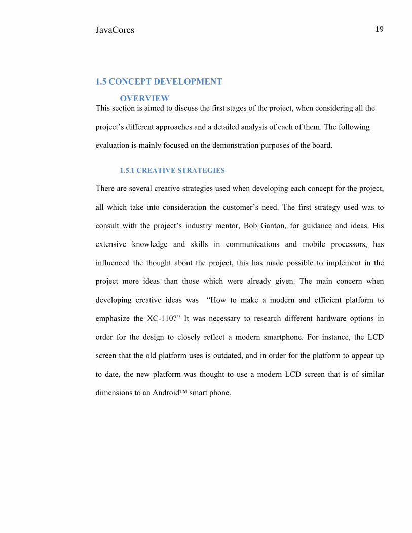
Use Existing Demonstration Kit (Slim Board)
This concept involves reviving the original XC-110 demonstration kit that was
developed several years ago by JavaCores.
Advantages:
• System has already been designed, simply needs to be updated and debugged
• It would give ample time to upgrade components, such as a touch-sensitive LCD
Disadvantages:
• Technology used in original demonstration kit is now outdated and therefore
would not truly demonstrate the Xpresso chip’s intended role in up and coming
mobile devices
• Would require an extensive amount of reverse-engineering
• Restrictions at the time to implement additional features on the board
FPGA
Host)Processor XC/110
LCD)CTRL
LCD
USB
PS2
PC
Keyboard
EEPROMFlash)
Memory Figure 8: Slim Board Schematic
JavaCores !
21!
1.5.2.2 Overall Concept II
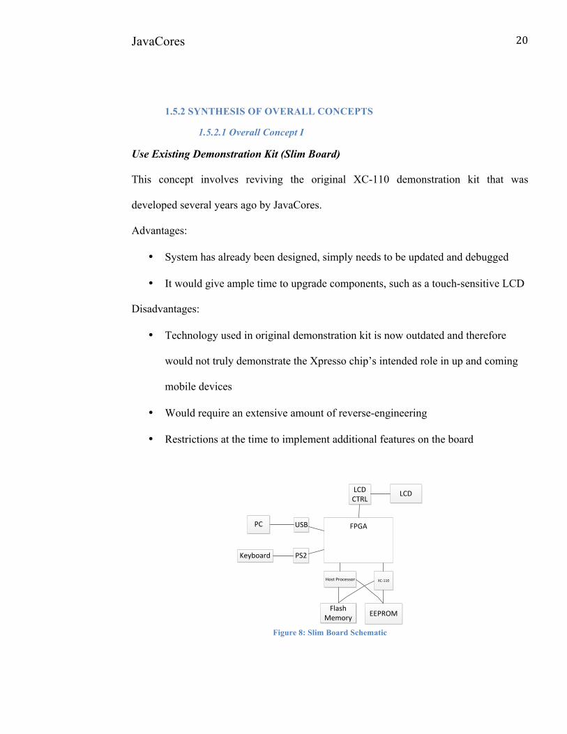
Develop a New Demonstration Kit
This concept involves creating an entirely new demonstration kit, similar to the original
kit, but using new and improved components that are now common in mobile devices.
Advantages:
• System can use new components that more closely reflect technology used in
current mobile devices
• System can be design to work as a daughter card of the PandaBoard
• System can be based off of original kit, making improvements where necessary
• Will not require reverse-engineering of the old work
Disadvantages:
• Need to design entire system from ground up, excluding VHDL code
FPGA
8051)Processor)&)Memory
XC5110
LCD)CTRL
LCD
Flash
USB
PS2
PC
Keyboard
Figure 9: New Demonstration Kit Preliminary Schematic
JavaCores !
22!
1.5.2.3 Overall Concept III
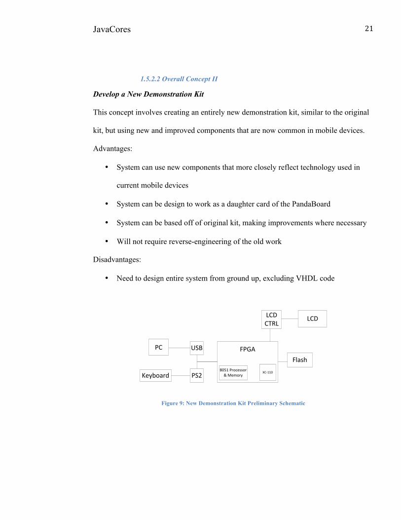
Implement XC-110 in an Existing Smartphone
This concept involves inserting the XC-110 into an existing smartphone that is on the
market. It would demonstrate that the chip is small enough to fit within current mobile
devices.
Advantages:
• Would show XC-110 in action in its intended location
• Performance of XC-110 easily be compared to a second smartphone of the same
model
Disadvantages:
• Space inside the phone is significantly constrained
• Would require a substantial amount of reverse engineering
Smartphone
Host-ProcessorLCD USB
PC
EEPROMFlash-Memory
FPGA
XC?110
Figure 10: Smartphone Integration Schematic
JavaCores !
23!
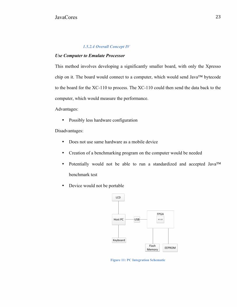
1.5.2.4 Overall Concept IV
Use Computer to Emulate Processor
This method involves developing a significantly smaller board, with only the Xpresso
chip on it. The board would connect to a computer, which would send Java™ bytecode
to the board for the XC-110 to process. The XC-110 could then send the data back to the
computer, which would measure the performance.
Advantages:
• Possibly less hardware configuration
Disadvantages:
• Does not use same hardware as a mobile device
• Creation of a benchmarking program on the computer would be needed
• Potentially would not be able to run a standardized and accepted Java™
benchmark test
• Device would not be portable
FPGA
XC'110
LCD
USBHost3PC
Keyboard
EEPROMFlash3
Memory
Figure 11: PC Integration Schematic
JavaCores !
24!
1.5.3 ANALYSIS OF THE OVERALL CONCEPTS
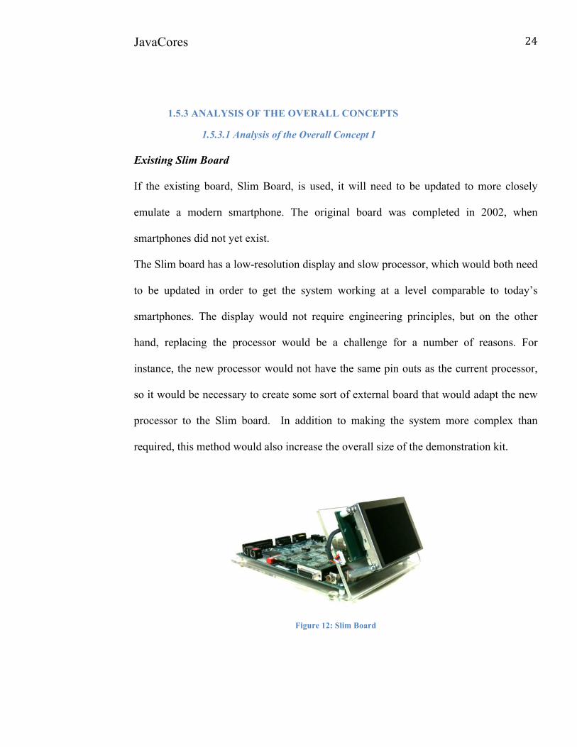
1.5.3.1 Analysis of the Overall Concept I Existing Slim Board
If the existing board, Slim Board, is used, it will need to be updated to more closely
emulate a modern smartphone. The original board was completed in 2002, when
smartphones did not yet exist.
The Slim board has a low-resolution display and slow processor, which would both need
to be updated in order to get the system working at a level comparable to today’s
smartphones. The display would not require engineering principles, but on the other
hand, replacing the processor would be a challenge for a number of reasons. For
instance, the new processor would not have the same pin outs as the current processor,
so it would be necessary to create some sort of external board that would adapt the new
processor to the Slim board. In addition to making the system more complex than
required, this method would also increase the overall size of the demonstration kit.
Figure 12: Slim Board
JavaCores !
25!
Modifying the Slim board would be advantageous because it wouldn’t be necessary to
design an entire board from scratch. Ideally, significant time would be saved taking this
route, and thus this extra time could be used to work on other technical improvements,
such as adding wireless communications, a touch screen interface, a camera, a
microphone, and extra memory.
1.5.3.2 Analysis of the Overall Concept 2 New Demonstration Kit
Creating a new demonstration kit will require much more engineering. Ideally, the
original Slim board schematic will be modified and a new board will be fabricated. The
resulting board will be smaller and more capable than the Slim board, because
technology has vastly improved in the past decade.
The current Slim board uses four Xilinx FPGA chips, which take up a significant
amount of surface area of the board. With modern FPGA chips, a single Xilinx Spartan 6
chip can be used in place of all four of the FPGA chips on the Slim board. Using a single
FPGA will greatly reduce the size, complexity, and cost of the new demonstration kit.
The FPGA would replace the XC-110.
Additionally, the new kit would use modern memory modules. In addition of the 1
gigabyte of DDR2 memory of the Panda Board, 1 gigabyte of memory of DDR3 and 8
megabyte of Flash memory will be implemented. The new memory modules are several
times smaller and faster than their predecessor, which results in the board’s size
reduction.
JavaCores !
26!
Furthermore, the XC-110 processor is integrated the processor into the Spartan 6 FPGA,
the most modern FPGA’s state of the art of the market. With the unused extra space on
the board, new features such as Bluetooth®, Wi-Fi, camera, and video will be
incorporated. As a result, the entire system will be more compact and portable,
compared to the existing Slim board, as well as adaptable to the PandaBoard.
While this system would allow for a more refined demonstration kit than simply reusing
the existing board, it will require a substantial amount of engineering to design this
complex of a board, although it is based off of an existing system.
1.5.3.3 Analysis of the Overall Concept 3
Existing Smartphone
Using an existing smartphone would be a great way to demonstrate how the XC-110
chip would fit into a modern smartphone. The resulting device would be something that
is familiar to the customer, allowing them to visualize the XC-110 in their product.
By purchasing an off the shelf smartphone, almost all of the electronic components
would be acquired, such as memory, a host processor, Bluetooth®, USB
communications, and a touch-sensitive LCD. This would save a significant amount of
time and money that is required to individually select and integrate each of these
components.
To add the XC-110 to the smartphone, a secondary board would need to be added. This
board could either be external or in place of the phone’s battery. Either way, integrating
this secondary board into the existing smartphone would be a huge challenge. The
JavaCores !
27!
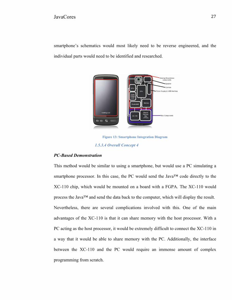
smartphone’s schematics would most likely need to be reverse engineered, and the
individual parts would need to be identified and researched.
Figure 13: Smartphone Integration Diagram
1.5.3.4 Overall Concept 4 PC-Based Demonstration
This method would be similar to using a smartphone, but would use a PC simulating a
smartphone processor. In this case, the PC would send the Java™ code directly to the
XC-110 chip, which would be mounted on a board with a FGPA. The XC-110 would
process the Java™ and send the data back to the computer, which will display the result.
Nevertheless, there are several complications involved with this. One of the main
advantages of the XC-110 is that it can share memory with the host processor. With a
PC acting as the host processor, it would be extremely difficult to connect the XC-110 in
a way that it would be able to share memory with the PC. Additionally, the interface
between the XC-110 and the PC would require an immense amount of complex
programming from scratch.

JavaCores !
28!
1.5.3 FINAL EVALUATION
1.5.3.1 Final Decision After a detailed analysis and evaluation of the four different concepts, it has been
determined that the best choice is to develop a new demonstration kit. It outstands in
terms of simplicity because this concept does not involve extensive reverse engineering
techniques. Another advantage is that this concept is the most robust. In contrast to the
outdated Slim Board, the new board will allow to adopt the design to current
technologies, making any necessary changes simpler. Furthermore, it will have
implemented the Spartan 6 FPGA. which will allow to the board to have numerous
multifunctional purposes.
However, this concept is not the most favorable in terms of costs since using the existing
demonstration board would be a less expensive alternative. Nevertheless, the Slim board
uses old technology that will difficult the process of advancing the product, and thus, the
main customer requirement, to bring the updated board to life, will never be met. In
order to balance this extra cost, a detailed analysis of funding, materials purchased, and
possible manufacture processes needs to be carefully calculated.
The second concept, developing a new demonstration kit, achieves the most remarkable
customer requirements. It is a portable device that has the precise size to allow the board
to have a USB 2.0 port for interfacing with the computer. It will function while running
Java™ code, and its performance will be faster due to the new upgraded technology of
the devices that are implemented. Furthermore, the way that its elements are distributed
JavaCores !
29!
along the board, internally and externally (with the PandaBoard), enhances its fast
processing speed and multipurpose uses.
1.5.3.2 Refinements The demonstration platform developed by JavaCores uses the Zucotto Application
Processor (ZAP) to implement the XC-110 and the Zucotto Interface. The Zucotto
Interface is a high-speed bus for connecting major system modules. Because the design
is outdated and complicated, there are many opportunities for refinements and
simplification:
• The old platform uses four FPGAs to implement the processor; The Panda
Xpresso uses only one FPGA, Spartan 6 from Xilinx, which has enough gates to
support the XC-110
• The external connection to the Panda Board will be used as a base platform
which main additional components include a host processor, a USD interface,
8Mb of Flash memory and wireless connectivity
• The memory, which is currently Toshiba™, will be replaced with modern DDR3
memory from Micron
• The overall size of the platform will be reduced
• The LCD to be incorporated has a higher resolution. Additionally, it is possible
to connect any other type of LCD, such as one with touch sensitive capabilities.
• The fact that the Panda Xpresso has implemented a Spartan 6 FPGA allows
exploring multiple opportunities including to incorporate a Bluetooth interface
JavaCores !
30!
on our platform. This would demonstrate the processor’s abilities to support a
modern feature of smart phones today
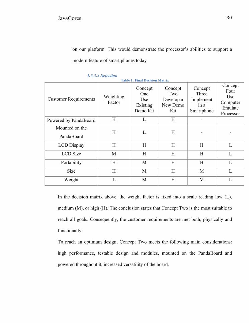
1.5.3.3 Selection Table 1: Final Decision Matrix
Customer Requirements Weighting Factor
Concept One Use
Existing Demo Kit
Concept Two
Develop a New Demo
Kit
Concept Three
Implement in a
Smartphone
Concept Four Use
Computer Emulate
Processor Powered by PandaBoard H L H - -
Mounted on the
PandaBoard H L H - -
LCD Display H H H H L
LCD Size M H H H L
Portability H M H H L
Size H M H M L
Weight L M H M L
In the decision matrix above, the weight factor is fixed into a scale reading low (L),
medium (M), or high (H). The conclusion states that Concept Two is the most suitable to
reach all goals. Consequently, the customer requirements are met both, physically and
functionally.
To reach an optimum design, Concept Two meets the following main considerations:
high performance, testable design and modules, mounted on the PandaBoard and
powered throughout it, increased versatility of the board.
JavaCores !
31!
1.6 DESIGN SPECIFICATIONS
1.6.1 BLOCK DIAGRAMS Appendix I include a block diagram that shows the individual features of both the
PandaBoard and the Panda Xpresso. Additionally, it shows how the two boards connect
and communicate with one another. It also gives a side-by-side comparison of the two
boards and clearly shows their similarities and differences.
1.6.2 GOVERNING PRINCIPLES The assembly of the mezzanine board, the Panda Xpresso, to the PandaBoard, involves
using an interpreted language (computer programming). A set of compiled code in
VHDL is to be implemented directly in hardware programming of a single Xilinx
Spartan 6 FPGA chip using the Xilinx IDE Design Suite. The PandaBoard acts as a host
processor that connects with the Spartan 6 of the Panda Xpresso. The Panda Xpresso,
core of the project, is essentially a daughter card for the PandaBoard that houses the
FPGA where the XC-110 is to be implemented. Therefore, the design involves
integrated circuit design, as well as processor function, VHDL code development, and
integration.
1.5.6.1 OVERALL DESIGN CONCEPT Because technology has vastly improved in the past decade, the resulting design of the
new board will be smaller and more capable than the previous demonstration board built
by JavaCores.
JavaCores !
32!
The outdated Slim board uses four Xilinx FPGA chips, which take up a significant
amount of surface area of the board. With modern FPGA chips, a single Xilinx Spartan 6
chip, which is currently a state of the art FPGAs, has more than enough room for a
mobile processor. Using a single FPGA greatly reduces the size, complexity, and cost of
the new demonstration kit. Additionally, it will allow the processor to implement more
efficiently and run at higher speeds. A detailed list of the Panda Xpresso is below.
• The Panda Xpresso features 1-gigabyte (GB) of DDR3 memory from Micron, in
addition to 1-gigabyte (GB) of DDR2 of the PandaBoard. In addition to the
DDR3 being capable of running faster than the DDR2, there is also an advantage
of having the DDR3 directly on the Panda Xpresso. With the DDR3 directly
accessible by the FPGA, the synthesized processor will be able to transfer data
back and forth with the DDR3, which will allow it to operate at the highest
possible speed.
• The Panda Xpresso contains two DACs and two ADCs, which can be used for
data acquisition and signal processing. These devices can communicate with the
PandaBoard through the FPGA. Because the PandaBoard runs Ubuntu, the
system eliminates the need for an external computer.
• The Panda Xpresso features a state-of-the-art Epson™ display controller, which
is optimized for mobile environments. The display controller is capable of
outputting to two LCDs simultaneously as well as taking input from a camera.
The display Kyocera™ WVGA TFT LCD connects to the Panda Xpresso via a
ribbon cable. Furthermore, there is a standard header in parallel with the ribbon
JavaCores !
33!
cable also included to ensure compatibility with any WVGA display.
Additionally, there is a serial LCD connector for a secondary WVGA display.
• The Panda Xpresso utilizes 8 MB of Xilinx platform flash, which allows the
device to be automatically programed at boot. This way the user does not have to
reprogram the FPGA with each power cycle.
By creating a new demonstration platform, the customer requirements have been
successfully reached. The new device is portable and conveniently sized, and connects
to the PandaBoard for communication and power. The board can be programmed to
contain the XC-110 processor and is also capable of running Android™ to emulate a
modern mobile environment.
1.5.6.2 FUNCTIONAL SPECIFICATIONS The following section describes how the design, construction and implementation of the
Panda Xpresso board meet the functional requirements.
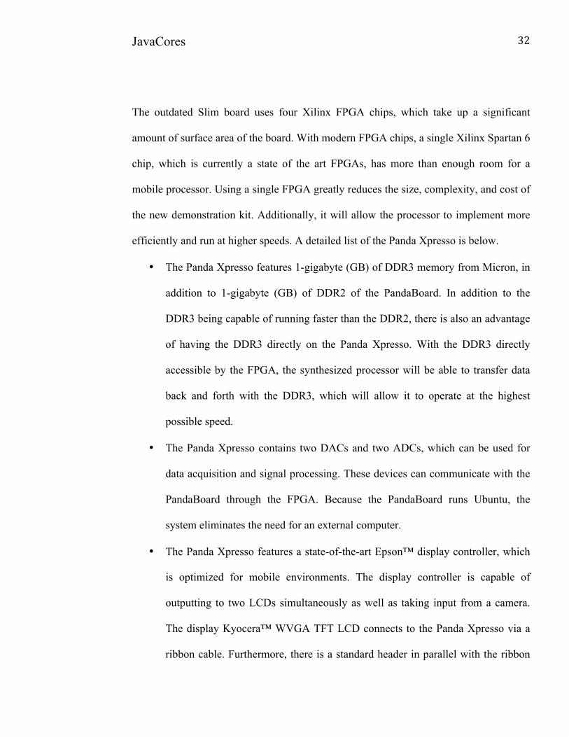
Each of the individual components, shown in Figure 7, is connected directly to the
FPGA. Depending on the application, the FPGA can send or receive data from the
PandaBoard and send that data to an external device, such as a display, DAC, or LED.
Additionally, the FGPA can take inputs from external components and process them
and/or send them to the PandaBoard.
JavaCores !
34!
Figure 14: Panda Xpresso Reduced Block Diagram
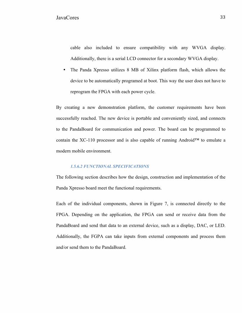
The Panda Xpresso does not include an LCD, but has been optimized for WVGA screen,
which is a standard resolution of modern mobile devices. While the board has been
designed specifically for a 4.3” Kyocera™ RGB WVGA display, the board is
compatible with any RGB or serial display with a resolution up to WVGA. A camera
input has been also included, which can be used for video processing applications.
Specifically, the XC-110 has been optimized to process video input from a camera and
the camera connector can help demonstrate this.
Figure 15: Panda Xpresso Display Block Diagram
JavaCores Final Design Report
13
The Panda Xpresso utilizes 8 MB of Xilinx platform flash, which allows the device to be automatically programed at boot. This way the user does not have to reprogram the FPGA with each power cycle.
By creating a new demonstration platform, the customer requirements have been successfully reached. The new device is portable and conveniently sized, and connects to the PandaBoard for communication and power. The board can be programmed to contain the XC-110 processor and is also capable of running Android™ to emulate a modern mobile environment.
Functional Specifications The following section describes how the design, construction and implementation of the board meet the functional requirements.
Each of the individual components, shown in Figure 4, is connected directly to the FPGA. Depending on the application, the FPGA can send or receive data from the PandaBoard and send that data to an external device, such as a display, DAC, or LED. Additionally, the FGPA can take inputs from external components and process them and/or send them to the PandaBoard.
Figure 2: Panda Xpresso Reduced Block Diagram
The Panda Xpresso does not include an LCD, but has been optimized for WVGA screen, which is a standard resolution of modern mobile devices. While the board has been designed specifically for a 4.3” Kyocera™ RGB WVGA display,
Panda Xpresso
FPGA
Memory
USB, RS-232, JTAG
Display
Buttons, Switches, & LEDs
ADCs & DACs
© 2012 JavaCores, Inc
7Monday, April 9, 12
JavaCores Final Design Report
14
the board is compatible with any RGB or serial display with a resolution up to WVGA. We have also included a camera input, which can be used for video processing applications. Specifically, the XC-110 has been optimized to process video input from a camera and the camera connector can help demonstrate this.
Figure 3: Panda Xpresso Display Block Diagram The two USB 2.0 ports are the only components on the Panda Xpresso that connect directly to the PandaBoard. The FPGA can still communicate with the USB ports, but must do so through the PandaBoard. The Panda Xpresso includes RS-232 and JTAG ports for direct programming and debugging.
Figure 4: Panda Xpresso USB/RS-232/JTAG Block Diagram
One of the most marketable features of the Panda Xpresso is the inclusion of
Panda Xpresso
FPGA
Memory
USB, RS-232, JTAG
Display
Buttons, Switches, & LEDs
ADCs & DACs
Display
Display
RGB Header 1
Display CTRL
RGB Header 1I
Serial Header Camera Input
FPGA
© 2012 JavaCores, Inc
7Monday, April 9, 12
Panda Xpresso
FPGA
Memory
USB, RS-232, JTAG
Display
Buttons, Switches, & LEDs
ADCs & DACs
USB, RS-232, JTAG
USB, RS-232, JTAG
USB
RS-232 CTRL RS-232
JTAGFPGA
PandaBoard
© 2012 JavaCores, Inc
7Monday, April 9, 12
JavaCores !
35!
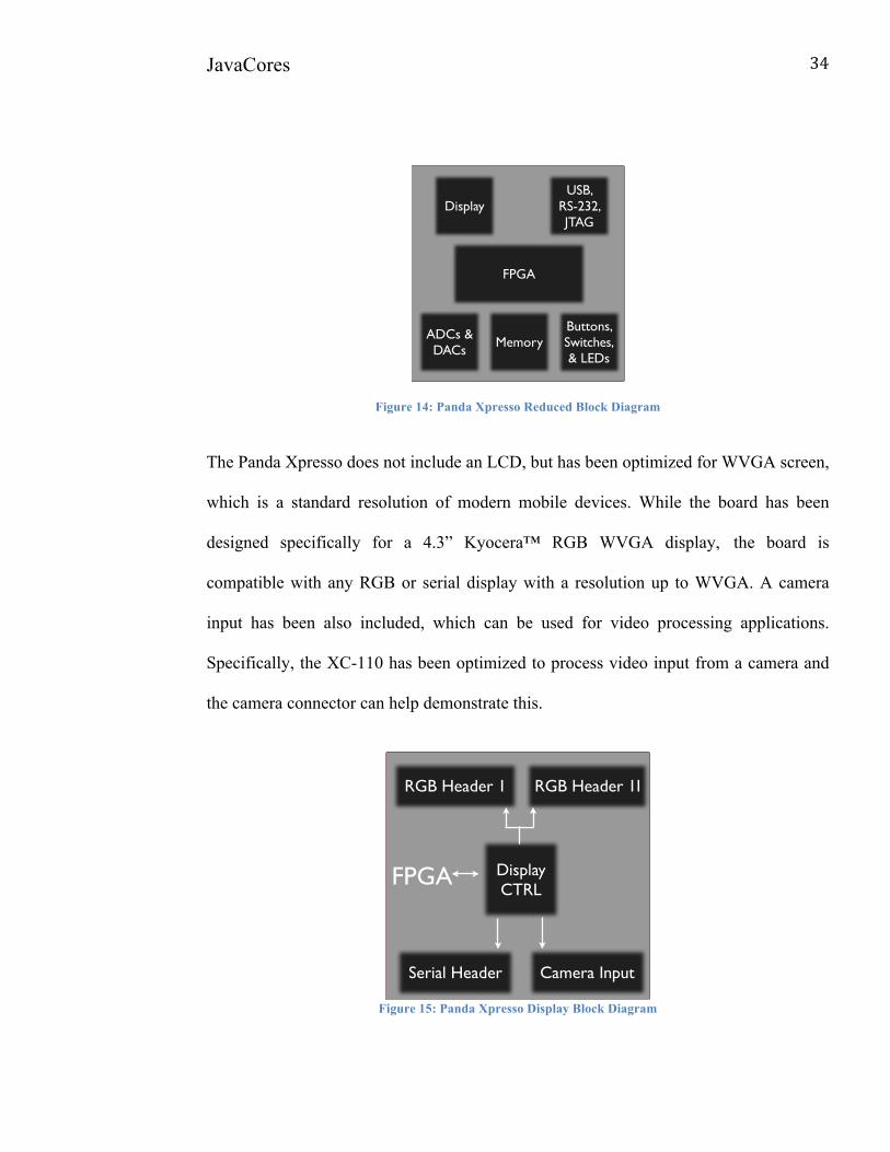
The two USB 2.0 ports are the only components on the Panda Xpresso that connect
directly to the PandaBoard. The FPGA can still communicate with the USB ports, but
must do so through the PandaBoard. The Panda Xpresso includes RS-232 and JTAG
ports for direct programming and debugging.
Figure 16: Panda Xpresso USB/ RS-232/ JATG Block Diagram
One of the most marketable features of the Panda Xpresso is the inclusion of multiple
DACs and ADCs. The DACs and ADCs will allow both hobbyists and professionals to
use the board for applications such as automated testing systems, measurement of analog
inputs, and creating analog outputs. The design includes the implementation of these
devices, although for budget purposes the Panda Xpresso board manufactured for this
project DNI them.
JavaCores Final Design Report
14
the board is compatible with any RGB or serial display with a resolution up to WVGA. We have also included a camera input, which can be used for video processing applications. Specifically, the XC-110 has been optimized to process video input from a camera and the camera connector can help demonstrate this.
Figure 3: Panda Xpresso Display Block Diagram The two USB 2.0 ports are the only components on the Panda Xpresso that connect directly to the PandaBoard. The FPGA can still communicate with the USB ports, but must do so through the PandaBoard. The Panda Xpresso includes RS-232 and JTAG ports for direct programming and debugging.
Figure 4: Panda Xpresso USB/RS-232/JTAG Block Diagram
One of the most marketable features of the Panda Xpresso is the inclusion of
Panda Xpresso
FPGA
Memory
USB, RS-232, JTAG
Display
Buttons, Switches, & LEDs
ADCs & DACs
Display
Display
RGB Header 1
Display CTRL
RGB Header 1I
Serial Header Camera Input
FPGA
© 2012 JavaCores, Inc
7Monday, April 9, 12
Panda Xpresso
FPGA
Memory
USB, RS-232, JTAG
Display
Buttons, Switches, & LEDs
ADCs & DACs
USB, RS-232, JTAG
USB, RS-232, JTAG
USB
RS-232 CTRL RS-232
JTAGFPGA
PandaBoard
© 2012 JavaCores, Inc
7Monday, April 9, 12
JavaCores !
36!
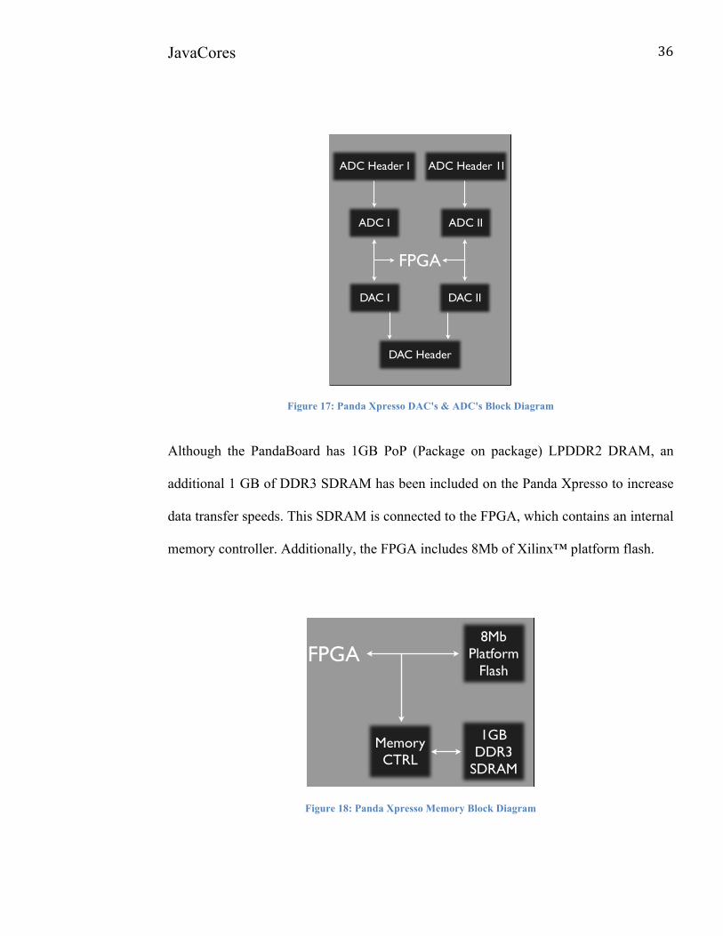
Figure 17: Panda Xpresso DAC's & ADC's Block Diagram
Although the PandaBoard has 1GB PoP (Package on package) LPDDR2 DRAM, an
additional 1 GB of DDR3 SDRAM has been included on the Panda Xpresso to increase
data transfer speeds. This SDRAM is connected to the FPGA, which contains an internal
memory controller. Additionally, the FPGA includes 8Mb of Xilinx™ platform flash.
Figure 18: Panda Xpresso Memory Block Diagram
JavaCores Final Design Report
15
multiple DACs and ADCs. The DACs and ADCs will allow both hobbyists and professionals to use the board for applications such as automated testing systems, measurement of analog inputs, and creating analog outputs. Our design includes the implementation of these devices, although for budget purposes we have decided to DNI them on our personal board.
Figure 5: Panda Xpresso DAC’s & ADC’s Block Diagram
Although the PandaBoard has 1GB PoP (Package on package) LPDDR2 DRAM, an additional 1 GB of DDR3 SDRAM has been included on the Panda Xpresso to increase data transfer speeds. This SDRAM is connected to the FPGA, which contains an internal memory controller. Additionally, the FPGA includes 8Mb of Xilinx™ platform flash.
Figure 6: Panda Xpresso memory Block Diagram
Panda Xpresso
FPGA
Memory
USB, RS-232, JTAG
Display
Buttons, Switches, & LEDs
ADCs & DACs
ADCs & DACs
ADCs & DACs
ADC Header I
ADC I
ADC Header 1I
ADC II
DAC I
DAC Header
DAC II
FPGA
© 2012 JavaCores, Inc
7Monday, April 9, 12
Panda Xpresso
FPGA
Memory
USB, RS-232, JTAG
Display
Buttons, Switches, & LEDs
ADCs & DACs Memory
Memory
Memory CTRL
8Mb Platform
FlashFPGA
1GB DDR3
SDRAM
© 2012 JavaCores, Inc
7Monday, April 9, 12
JavaCores !
37!
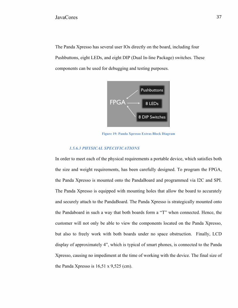
The Panda Xpresso has several user IOs directly on the board, including four
Pushbuttons, eight LEDs, and eight DIP (Dual In-line Package) switches. These
components can be used for debugging and testing purposes.
Figure 19: Panda Xpresso Extras Block Diagram
1.5.6.3 PHYSICAL SPECIFICATIONS In order to meet each of the physical requirements a portable device, which satisfies both
the size and weight requirements, has been carefully designed. To program the FPGA,
the Panda Xpresso is mounted onto the PandaBoard and programmed via I2C and SPI.
The Panda Xpresso is equipped with mounting holes that allow the board to accurately
and securely attach to the PandaBoard. The Panda Xpresso is strategically mounted onto
the Pandaboard in such a way that both boards form a “T” when connected. Hence, the
customer will not only be able to view the components located on the Panda Xpresso,
but also to freely work with both boards under no space obstruction. Finally, LCD
display of approximately 4”, which is typical of smart phones, is connected to the Panda
Xpresso, causing no impediment at the time of working with the device. The final size of
the Panda Xpresso is 16,51 x 9,525 (cm).
JavaCores Final Design Report
16
The Panda Xpresso has several user IOs directly on the board, including four pushbuttons eight LEDs, and eight DIP (Dual In-line Package) switches. These components can be used for debugging and testing purposes.
Figure 7:Panda Xpresso User IOs Block Diagram
Physical Specifications In order to meet each of the physical requirements we have designed a portable device, which satisfies both the size and weight requirements as listed under Physical Requirements. To program the FPGA the Panda Xpresso is mounted onto the PandaBoard and programmed via I2C and SPI. The Panda Xpresso is equipped with mounting holes that allow the Panda Xpresso to accurately and securely attach to the PandaBoard. The final size of the Panda Xpresso is 6.5” x 3.75” (165.1mm x 95.25mm). Therefore, the size of the design has decreased drastically.
Design Analysis and Results System Analysis and Design
Software
The primary software the team has utilized is Proteus PCB Design Suite, which includes both ARES and ISIS. ISIS was used to create the schematic for the Panda Xpresso, and ARES was used to design the layout and route the board. Additionally, Xilinx ISE 13.4 was used to create the VHDL program for the verification of the FPGA. Ubuntu 12.04 was also installed on the PandaBoard, which was installed through a command line through a separate Linux computer.
Panda Xpresso
FPGA
Memory
USB, RS-232, JTAG
Display
Buttons, Switches, & LEDs
ADCs & DACs
Buttons, Switches, & LEDs
Buttons, Switches, & LEDs
Pushbuttons
8 LEDsFPGA
8 DIP Switches
© 2012 JavaCores, Inc
7Monday, April 9, 12
JavaCores !
38!
1.7 SYSTEM ANALYSIS AND DESIGN
1.7.1 SOFTWARE
• The primary software that has been utilized is Proteus PCB Design Suite, which
includes both ARES and ISIS. ISIS was used to create the schematic for the
Panda Xpresso, and ARES was used to design the layout and route the board.
Additionally, Xilinx ISE 13.4 was used to create the VHDL program for the
verification of the FPGA. Ubuntu 12.04 was also installed on the PandaBoard,
which was installed through a command line through a separate Linux computer.
• Originally, the projects involved the recovering of the XC-110 processor’s
VHDL design. However due to time constrains, it was determined by the
industry mentor, Bob Ganton, that a separate software team with Android™ and
Java™ experience would have to modify the code in order for it to be
implemented properly.
• A simple VHDL verification program, which uses LEDs and switches, has been
designed in Xilinx ISE 13.4 and implemented on the Spartan 3A Development
Kit. A program written in C has also been developed.
1.7.2 HARDWARE
• The PCB has an eight-layer board stack up with a final thickness of .062”
(1.575mm) and half ounce copper traces. The board was manufactured using
standard FR4 material by Accutrace, Inc. In order to reduce cost, and at the same
time, deal with size constraints of the display controller’s BGA; the routing was
completed with micro vias and vias in pad (instead of using blind vias). The
JavaCores !
39!
minimum trace width was 3 mils (0.0762 mm) and the minimum spacing
between components was 5 mils (0.127 mm).
• Once the PandaBoard was received, it was necessary to immediately verify that it
worked properly. The PandaBoard was ordered from Digikey and provided by
the industry mentor.
• A Spartan 3A Evaluation Kit (EVK) has been additionally acquired to develop
the VHDL code while the Panda Xpresso was being produced.
1.7.3 SUBSYSTEM ANALYSIS AND DESIGN The subsystems that have been completed in the course of the project include developing
the schematic for the Panda Xpresso PCB, developing the layout, completing the routing
for the PCB, and installing the correct software onto the PandaBoard and Panda
Xpresso.
1.7.3.1 SUBSYSTEM 1 The first subsystem consisted of developing the schematic for the Panda Xpresso board.
The schematic was created using Proteus PCB Design software (ISIS). Throughout the
PCB design it was fundamental to consult the following reference schematics: Avnet
Spartan 6 Development Kit and the PandaDAQ. Mark Haun, the creator of the
PandaBoard, has improved the course of the project by providing with the PandaDAQ
and also by personally solving some of the project’s concerns. Furthermore, for the
schematic design it has been necessary to create the individual footprints for each of the
parts of the schematic. Later on it was needed to carefully double-check each component
JavaCores !
40!
to ensure that their size and the pin-outs were correct. Moreover, the design was
thoroughly reviewed by Bob Ganton. In addition multiple test points were added to the
design. The test points have been mainly located on power sources, clock signals and
crystal oscillators. The design of the Panda Xpresso schematic took eighth weeks to be
completed and it is thirteen pages length. A copy of it can be found in Document N. 2
Planes.
1.7.3.2 SUBSYSTEM 2 The next step subsystem consisted in designing the layout of the Panda Xpresso PCB.
The layout has been created using Proteus PCB Design software (ARES). Each
component required its own footprint; the marks were designed using ARES. In order to
create these footprints, the datasheets were referenced and each component was
measured and verified. Before starting with the design, it was required to study different
BGA breakout methods. Certain components, such as the DDR3 needed certain routing
techniques, which included routing the traces so that their lengths were different by no
more than eight millimeters. The widths of these traces were also increased from 3 mils
(0.0762 mm) to 5 mils (0.127 mm) in order to match the impedances.
The display controller had the smallest pitch and therefore required the use of vias in pad
instead of micro vias. The use of vias in pad resulted in a small increase in
manufacturing costs, although it was less expensive than using micro vias.
1.7.3.3 SUBSYSTEM 3 The final subsystem consisted of developing the VHDL program that would verify the
JavaCores !
41!
functionality of the FPGA on the Panda Xpresso, as well as the communication between
the Panda Xpresso and PandaBoard. This involved writing a VHDL code and a program
written in C that uploads the VHDL bitfile directly to the Panda Xpresso from the
PandaBoard. The VHDL code was written in Xilinx ISE 13.4 and includes a UCF of the
entire Panda Xpresso FPGA, as well as a small verification program.
1.8 CALCULATIONS The project has not involved complicated arithmetic computations. Nevertheless, it has
been required to calculate the values of the resistors of the different voltage regulators,
as well as the value of the lengths of the traces that connect the DDR3 memory with the
FPGA.
1.8.1 RESISTORS’ VALUES The resistors implemented in each of the voltage regulators have been selected
according with resistor divider formulas, which were given in the datasheet of each of
these components. Only two types of voltage regulators have been implemented on the
board’s schematics; X of AP7167 and Y of SC4216, both designed for applications
requiring very low input and dropout voltages.
The value of the resistors have been finally calculated following the mathematical
relationship obtained after plugging the values of the different desired output voltages
into the equations below:
!" = !"#$(1+ !1!2)
Equation 1: AP7167 Voltage Regulator

JavaCores !
42!
!" = 0.5(!1+ !2)!2
Equation 2: SC4216 Voltage Regulator
For equation 1: R1= 0.25*R2 (Vref=0.8, internal reference voltage)
For equation 2: R1=(2Vo -1)*R2
Table 2: Numerical Results of Resistor's Values
Voltage Regulator Desired Vout (V) R1(Ohm) R2(Ohm)
SC4216 2.5 102K 25.5K
SC4216 1.2 - -
AP7167 1.8 15K 12K
AP7167 1.5 11.3K 13K
AP7167 3.3 10K 2.20K+1.0K
1.8.2 DDR3 TRACE LENGTHS The computations of the lengths of the DDR3’s traces are needed to determine their
associated impedances and, consequently, the thermal requirements that the Panda
Xpresso has to meet.
The calculations related with this section have been based on simple additions. Although
the mathematical method is elementary, consisting only in adding decimal numbers, the
procedure to measure the traces has been very tedious. While measuring the trace
lengths on the lay out (using the software ARES), it has been needed to dissect each of

JavaCores !
43!
the 28 traces that connect the DDR3 memory with the FPGA in different segments; each
of these segments corresponds to a single layer.
Following is a table that gathers the total dimension of each trace, as well as the
dimensions of each of its segments:

JavaCores !
44!
Table 3: DDR3 Trace LengthsSignal Name DDR3 Pin FPGA Pin Top Copper Inner Layer 1 Inner Layer 4 Inner Layer 5 Inner Layer 6 Bottom
CopperTotal Length
(mm)DDR3_DATA
_13 A2 20.068 0 0 0 0 0 20.068
DDR3_DATA_11 C2 R1 20 0 0 0 0 0 20
DDR3_DATA_2 F2 M2 22 0 0 0 0 0 22
DDR3_DATA_6 G2 K2 22 0 0 0 0 0 22
L2 0.507 0 0 3.28 0 0.613 4.3DDR3_BA0 M2 0.507 0 0 0 0 25.61 30DDR3_ADD
R_3 N2 3.845 0 0 0 33.15 38
DDR3_ADDR_5 P2 22 0 0 0 0 0 22
DDR3_ADDR_7 R2 2 18.096 0 0 2.904 0 23
DDR3_RST T2 22 0 0 0 0 0 22DDR3_DATA
_0 C3 2.581 0 0 0 0 4.581 23
DDR3_UDM D3 6.415 0 0 0 0 18.419 23DDR3_DATA
0 E3 5.514 0 18.486 0 0 0 24
DDR3_LDQS F3 1.014 6.566 0 0 0 16.42 24
DDR3_LDQS# G3 4.395 0 18.605 0 0 0 23
DDR3_DATA4 H3 16.615 8.385 0 0 0 0 25
DDR3_RAS# J3 1.014 23.986 0 0 0 0 25
DDR3_CAS# K3 19.334 8.006 0 0 0 0 28
DDR3_BA2 M3 5.802 0 0 0 0 17.198 23DDR3_ADD
R0 N3 1.014 17.196 11.79 0 0 0 30
DDR3_ADDR2 P3 1.053 23.947 0 0 0 0 25
DDR3_ADDR9 R3 22 0 0 0 0 0 22
DDR3_DATA12 A7 5.7063 0 21.29 0 0 0 27
DDR3_UDQS# B7 4.367 0 22.63 0 0 0 27
DDR3_UDQS C7 6.507 0 22 0 0 0 29
DDR3_DATA8 D7 20.766 7.234 0 0 0 0 29
DDR3_LDM E7 10.592 0 17.408 0 0 0 28DDR3_DATA
_1 F7 20.58 9.42 0 0 0 0 30
1.9 ECONOMIC RESEARCH
1.9.1 VIABILITY The ideal scenario of the project is to implement the VHDL code of XC-110 (written by
JavaCores) onto the FPGA. However, a second more likely scenario has been pursued.
The deciding factors that have pushed the project towards the second option are related
JavaCores !
45!
to time constrains. In order to assure that the Panda Xpresso would be ready for
merchandising, all the process involving the scrutiny of the specific XC-110 code (on
the bulk of data provided by JavaCores) has been reduced to a much simpler task. The
new task consists on finding a simpler piece of the FPGA code. An input, for instance a
sine wave generated by the oscilloscope, is processed and, the output is simultaneously
displayed on the LCD. Therefore this demonstration will be showing only a small
portion of the microprocessor’s performance.
More important, this decision has been made by client request. The client has always
been skeptical about the fulfillment of the code synthesis work. Not only for the
complications at the time of finding the suitable code, but also due to the fact that there
are different versions of the Xilinx software. The former implies that the given VHDL
code also needs minor edits in order to be compatible with the newer versions of Xilinx.
1.9.2 ECONOMIC INTEREST The first notion of this project involved to built a new demonstration platform board for
the XC-110 microprocessor. Because of the outstanding XC-110’s capabilities, the
microprocessor was targeted towards major smartphones/tablet producers such as
Google and Samsung. JavaCores had predicted that every new mobile platform running
Java™ would carry the XC-110. However, rather than producing and marketing it
individually, JavaCores had planned to sell the product directly to mobile producers.
The revenues obtained from the sale of the microprocessor were estimated to reach
$30M.
JavaCores !
46!
Nevertheless, after the analysis of the initial project’s low viability (previously
discussed), the client decided to give more versatility to the project, and explode the
wide range of uses that the Panda Xpresso could hold. The attractiveness of the new
board is its multipurpose functions. For instance, whereas a single automated testing
system board is sold for an approximate price of $200, the Panda Xpresso board can be
sold for a slightly higher price. Thus, due to its numerous uses, the boards that work for
single purposes wont even be direct competitors of the Panda Xpresso.
JavaCores’ plans are to sell the mezzanine card for $399, and to personally operate and
distribute its own product line. The Panda Xpresso board is expected to be as recognized
as the British Raspberry Pi, this is the reason of JavaCores’ high revenues expectations.
Moreover, the project is the foundation for a later design focused on the XC-110. In this
sense the Panda Xpresso board, although not being a monetary reward, it is a great step
towards the millionaire project initially thought by the client.1.10 APPENDIX
JavaCores !
47!
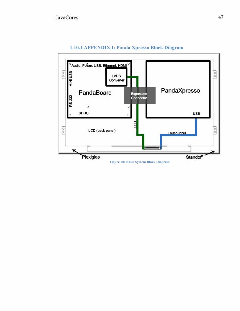
1.10.1 APPENDIX I: Panda Xpresso Block Diagram
Figure 20: Basic System Block Diagram
LCD (back panel)Touch Input
LCD
Plexiglas
SDHC USB
PandaXpressoPandaBoard
LVDS
Converter
Audio, Power, USB, Ethernet, HDMI
Standoff
RS-232 MINI USB
LCD
Expansion
Connector
Audio, Power, USB, Ethernet, HDMI
JavaCores !
48!
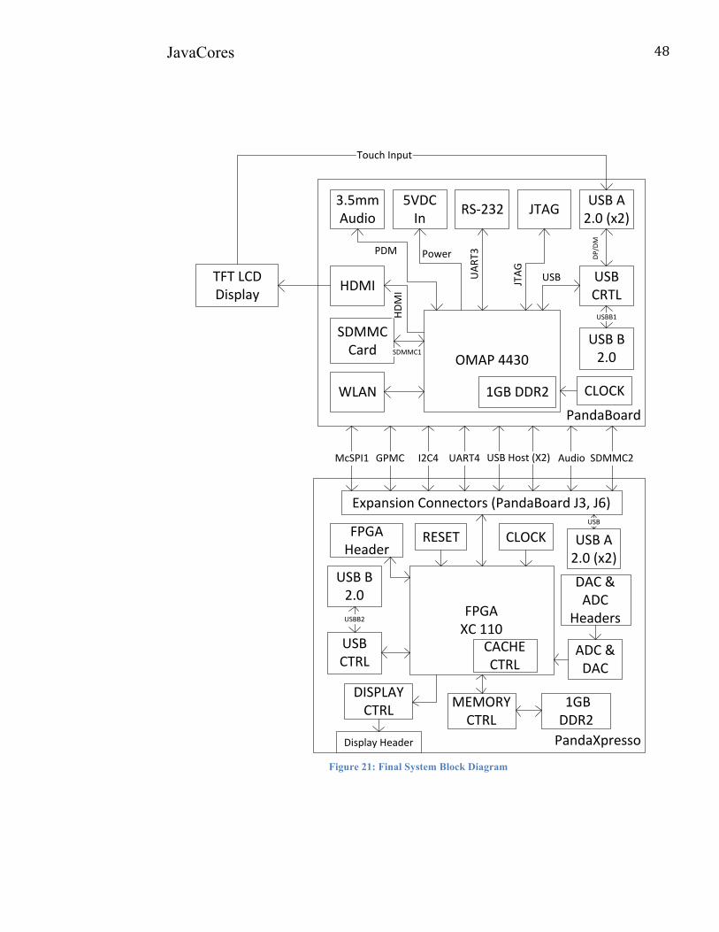
Figure 21: Final System Block Diagram
PandaXpresso
FPGAXC 110
CACHE CTRL
DISPLAY CTRL
TFT LCD Display
Expansion Connectors (PandaBoard J3, J6)
PandaBoard
1GB DDR2
SDMMC Card
MEMORY CTRL
GPMC
CLOCKRESET
USB A 2.0 (x2)
OMAP 4430
1GB DDR2
USB CRTL
5VDC In JTAG
CLOCK
RS-232
WLAN
3.5mm Audio
HDMI
DP/D
M
USBJTAGUAR
T3PowerPDM
HDM
I
SDMMC1
I2C4 UART4 USB Host (X2)McSPI1 Audio SDMMC2
USB A 2.0 (x2)DAC &
ADC Headers
USB B 2.0
USB CTRL
ADC & DAC
USB
USBB2
USB B 2.0
USBB1
Touch Input
Display Header
FPGA Header
JavaCores !
49!
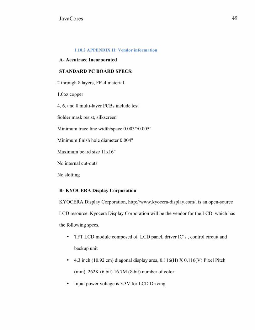
1.10.2 APPENDIX II: Vendor information
A- Accutrace Incorporated STANDARD PC BOARD SPECS:
2 through 8 layers, FR-4 material
1.0oz copper
4, 6, and 8 multi-layer PCBs include test
Solder mask resist, silkscreen
Minimum trace line width/space 0.003"/0.005"
Minimum finish hole diameter 0.004"
Maximum board size 11x16"
No internal cut-outs
No slotting
B- KYOCERA Display Corporation
KYOCERA Display Corporation, http://www.kyocera-display.com/, is an open-source
LCD resource. Kyocera Display Corporation will be the vendor for the LCD, which has
the following specs.
• TFT LCD module composed of LCD panel, driver IC’s , control circuit and
backup unit
• 4.3 inch (10.92 cm) diagonal display area, 0.116(H) X 0.116(V) Pixel Pitch
(mm), 262K (6 bit) 16.7M (8 bit) number of color
• Input power voltage is 3.3V for LCD Driving
JavaCores !
50!
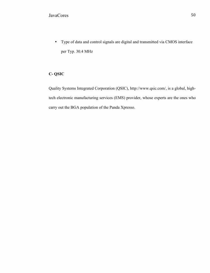
• Type of data and control signals are digital and transmitted via CMOS interface
per Typ. 30.4 MHz
C- QSIC
Quality Systems Integrated Corporation (QSIC), http://www.qsic.com/, is a global, high-
tech electronic manufacturing services (EMS) provider, whose experts are the ones who
carry out the BGA population of the Panda Xpresso.
JavaCores !
51!
1.10.3 APPENDIX III: PATENTS
JavaCores !
52!
1.10.4 APPENDIX IV: COMMONLY USED ACRONYMS ADC Analog-to-Digital Converter BGA Ball Grid Array DAC Digital-to-Analog Converter DDR Double Data Rate DNI Do Not Include DSP Digital Signal Processing JVM Java Virtual Machine EVK Evaluation kit FPGA Field Programmable Gate Array GND Ground I2C Inter-Integrated Circuit; generally referred to as two-wire interface I/O Input-Output JTAG Joint Test Action Group JVM Java Virtual Machine LAN Local Area Network LED Light Emitting Diode LCD Liquid Crystal Display MB Megabyte (1024 bytes) PCB Printed Circuit Board RAM Random Access Memory RGB Red Green Blue SDRAM Synchronous Dynamic RAM SoC System on Chip SPI Serial Peripheral Interface TFT Thin Film Transistor UCF User Constraints File USB Universal Serial Bus VHDL
Very High Speed Integrated Circuit Hardware Description Language
WLAN Wireless LAN, also known as WiFi WVGA Wide Video Graphics Array (800x480 pixels) XC-110 Xpresso Core Java Processor
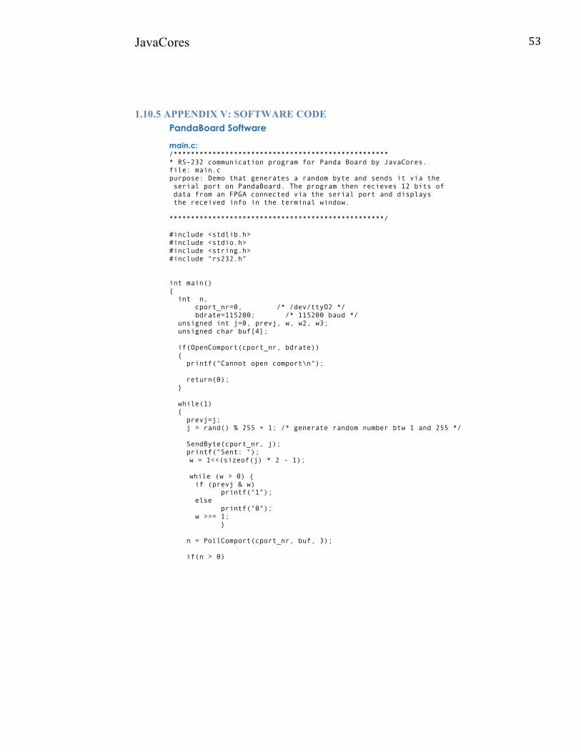
JavaCores !
53!
1.10.5 APPENDIX V: SOFTWARE CODE
JavaCores Final Design Report
58
Appendix G: Software
PandaBoard Software
main.c: /************************************************** * RS-232 communication program for Panda Board by JavaCores. file: main.c purpose: Demo that generates a random byte and sends it via the serial port on PandaBoard. The program then recieves 12 bits of data from an FPGA connected via the serial port and displays the received info in the terminal window. **************************************************/ #include <stdlib.h> #include <stdio.h> #include <string.h> #include "rs232.h" int main() { int n, cport_nr=0, /* /dev/ttyO2 */ bdrate=115200; /* 115200 baud */ unsigned int j=0, prevj, w, w2, w3; unsigned char buf[4]; if(OpenComport(cport_nr, bdrate)) { printf("Cannot open comport\n"); return(0); } while(1) { prevj=j; j = rand() % 255 + 1; /* generate random number btw 1 and 255 */ SendByte(cport_nr, j); printf("Sent: "); w = 1<<(sizeof(j) * 2 - 1); while (w > 0) { if (prevj & w) printf("1"); else printf("0"); w >>= 1; } n = PollComport(cport_nr, buf, 3); if(n > 0)
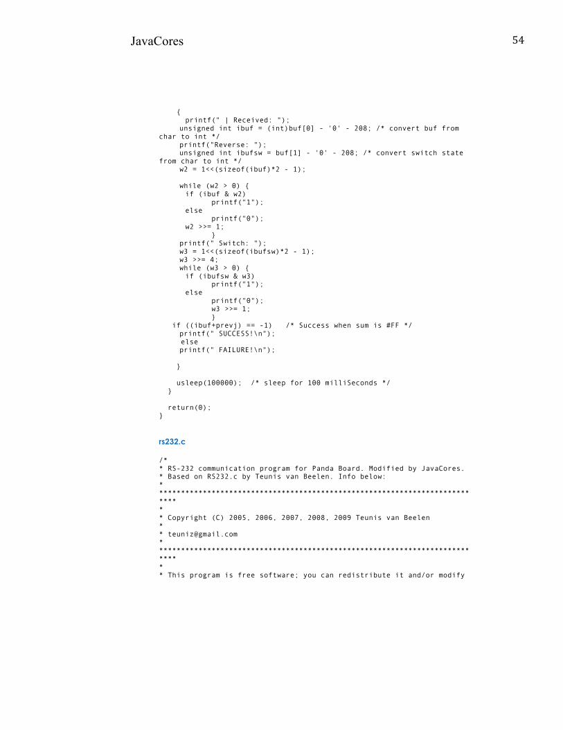
JavaCores !
54!
JavaCores Final Design Report
59
{ printf(" | Received: "); unsigned int ibuf = (int)buf[0] - '0' - 208; /* convert buf from char to int */ printf("Reverse: "); unsigned int ibufsw = buf[1] - '0' - 208; /* convert switch state from char to int */ w2 = 1<<(sizeof(ibuf)*2 - 1); while (w2 > 0) { if (ibuf & w2) printf("1"); else printf("0"); w2 >>= 1; } printf(" Switch: "); w3 = 1<<(sizeof(ibufsw)*2 - 1); w3 >>= 4; while (w3 > 0) { if (ibufsw & w3) printf("1"); else printf("0"); w3 >>= 1; } if ((ibuf+prevj) == -1) /* Success when sum is #FF */ printf(" SUCCESS!\n"); else printf(" FAILURE!\n"); } usleep(100000); /* sleep for 100 milliSeconds */ } return(0); }
rs232.c /* * RS-232 communication program for Panda Board. Modified by JavaCores. * Based on RS232.c by Teunis van Beelen. Info below: * *************************************************************************** * * Copyright (C) 2005, 2006, 2007, 2008, 2009 Teunis van Beelen * * [email protected] * *************************************************************************** * * This program is free software; you can redistribute it and/or modify
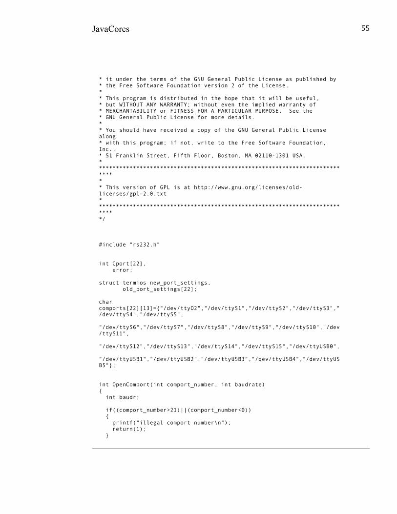
JavaCores !
55!
JavaCores Final Design Report
60
* it under the terms of the GNU General Public License as published by * the Free Software Foundation version 2 of the License. * * This program is distributed in the hope that it will be useful, * but WITHOUT ANY WARRANTY; without even the implied warranty of * MERCHANTABILITY or FITNESS FOR A PARTICULAR PURPOSE. See the * GNU General Public License for more details. * * You should have received a copy of the GNU General Public License along * with this program; if not, write to the Free Software Foundation, Inc., * 51 Franklin Street, Fifth Floor, Boston, MA 02110-1301 USA. * *************************************************************************** * * This version of GPL is at http://www.gnu.org/licenses/old-licenses/gpl-2.0.txt * *************************************************************************** */ #include "rs232.h" int Cport[22], error; struct termios new_port_settings, old_port_settings[22]; char comports[22][13]={"/dev/ttyO2","/dev/ttyS1","/dev/ttyS2","/dev/ttyS3","/dev/ttyS4","/dev/ttyS5", "/dev/ttyS6","/dev/ttyS7","/dev/ttyS8","/dev/ttyS9","/dev/ttyS10","/dev/ttyS11", "/dev/ttyS12","/dev/ttyS13","/dev/ttyS14","/dev/ttyS15","/dev/ttyUSB0", "/dev/ttyUSB1","/dev/ttyUSB2","/dev/ttyUSB3","/dev/ttyUSB4","/dev/ttyUSB5"}; int OpenComport(int comport_number, int baudrate) { int baudr; if((comport_number>21)||(comport_number<0)) { printf("illegal comport number\n"); return(1); }
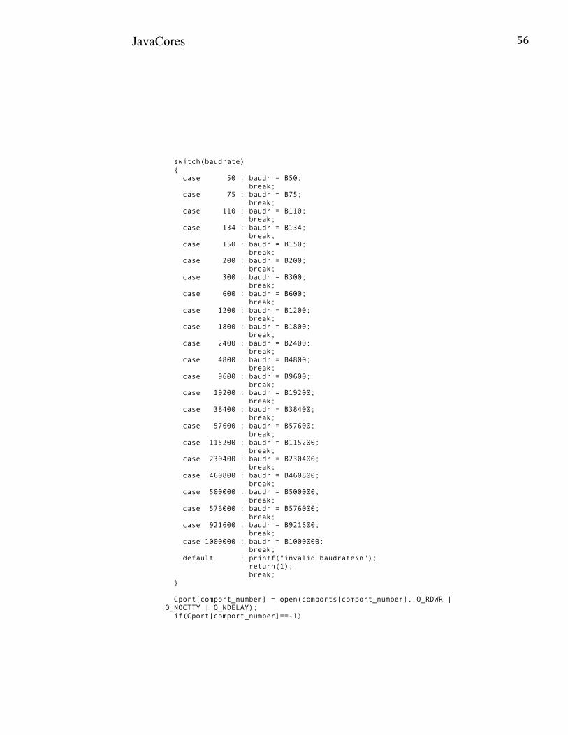
JavaCores !
56!
JavaCores Final Design Report
61
switch(baudrate) { case 50 : baudr = B50; break; case 75 : baudr = B75; break; case 110 : baudr = B110; break; case 134 : baudr = B134; break; case 150 : baudr = B150; break; case 200 : baudr = B200; break; case 300 : baudr = B300; break; case 600 : baudr = B600; break; case 1200 : baudr = B1200; break; case 1800 : baudr = B1800; break; case 2400 : baudr = B2400; break; case 4800 : baudr = B4800; break; case 9600 : baudr = B9600; break; case 19200 : baudr = B19200; break; case 38400 : baudr = B38400; break; case 57600 : baudr = B57600; break; case 115200 : baudr = B115200; break; case 230400 : baudr = B230400; break; case 460800 : baudr = B460800; break; case 500000 : baudr = B500000; break; case 576000 : baudr = B576000; break; case 921600 : baudr = B921600; break; case 1000000 : baudr = B1000000; break; default : printf("invalid baudrate\n"); return(1); break; } Cport[comport_number] = open(comports[comport_number], O_RDWR | O_NOCTTY | O_NDELAY); if(Cport[comport_number]==-1)
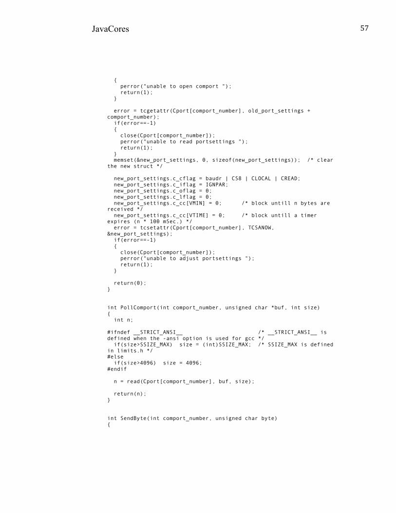
JavaCores !
57!
JavaCores Final Design Report
62
{ perror("unable to open comport "); return(1); } error = tcgetattr(Cport[comport_number], old_port_settings + comport_number); if(error==-1) { close(Cport[comport_number]); perror("unable to read portsettings "); return(1); } memset(&new_port_settings, 0, sizeof(new_port_settings)); /* clear the new struct */ new_port_settings.c_cflag = baudr | CS8 | CLOCAL | CREAD; new_port_settings.c_iflag = IGNPAR; new_port_settings.c_oflag = 0; new_port_settings.c_lflag = 0; new_port_settings.c_cc[VMIN] = 0; /* block untill n bytes are received */ new_port_settings.c_cc[VTIME] = 0; /* block untill a timer expires (n * 100 mSec.) */ error = tcsetattr(Cport[comport_number], TCSANOW, &new_port_settings); if(error==-1) { close(Cport[comport_number]); perror("unable to adjust portsettings "); return(1); } return(0); } int PollComport(int comport_number, unsigned char *buf, int size) { int n; #ifndef __STRICT_ANSI__ /* __STRICT_ANSI__ is defined when the -ansi option is used for gcc */ if(size>SSIZE_MAX) size = (int)SSIZE_MAX; /* SSIZE_MAX is defined in limits.h */ #else if(size>4096) size = 4096; #endif n = read(Cport[comport_number], buf, size); return(n); } int SendByte(int comport_number, unsigned char byte) {
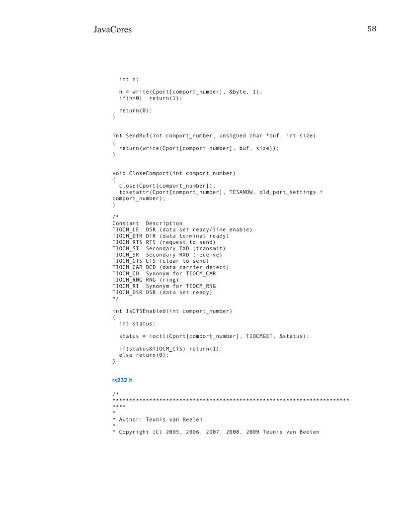
JavaCores !
58!
JavaCores Final Design Report
63
int n; n = write(Cport[comport_number], &byte, 1); if(n<0) return(1); return(0); } int SendBuf(int comport_number, unsigned char *buf, int size) { return(write(Cport[comport_number], buf, size)); } void CloseComport(int comport_number) { close(Cport[comport_number]); tcsetattr(Cport[comport_number], TCSANOW, old_port_settings + comport_number); } /* Constant Description TIOCM_LE DSR (data set ready/line enable) TIOCM_DTR DTR (data terminal ready) TIOCM_RTS RTS (request to send) TIOCM_ST Secondary TXD (transmit) TIOCM_SR Secondary RXD (receive) TIOCM_CTS CTS (clear to send) TIOCM_CAR DCD (data carrier detect) TIOCM_CD Synonym for TIOCM_CAR TIOCM_RNG RNG (ring) TIOCM_RI Synonym for TIOCM_RNG TIOCM_DSR DSR (data set ready) */ int IsCTSEnabled(int comport_number) { int status; status = ioctl(Cport[comport_number], TIOCMGET, &status); if(status&TIOCM_CTS) return(1); else return(0); }
rs232.h /* *************************************************************************** * * Author: Teunis van Beelen * * Copyright (C) 2005, 2006, 2007, 2008, 2009 Teunis van Beelen
JavaCores !
59!
JavaCores Final Design Report
64
* * [email protected] * *************************************************************************** * * This program is free software; you can redistribute it and/or modify * it under the terms of the GNU General Public License as published by * the Free Software Foundation version 2 of the License. * * This program is distributed in the hope that it will be useful, * but WITHOUT ANY WARRANTY; without even the implied warranty of * MERCHANTABILITY or FITNESS FOR A PARTICULAR PURPOSE. See the * GNU General Public License for more details. * * You should have received a copy of the GNU General Public License along * with this program; if not, write to the Free Software Foundation, Inc., * 51 Franklin Street, Fifth Floor, Boston, MA 02110-1301 USA. * *************************************************************************** * * This version of GPL is at http://www.gnu.org/licenses/old-licenses/gpl-2.0.txt * *************************************************************************** */ #ifndef rs232_INCLUDED #define rs232_INCLUDED #ifdef __cplusplus extern "C" { #endif #include <stdio.h> #include <string.h> #ifdef __linux__ #include <termios.h> #include <sys/ioctl.h> #include <unistd.h> #include <fcntl.h> #include <sys/types.h> #include <sys/stat.h> #include <limits.h> #else
JavaCores !
60!
JavaCores Final Design Report
65
#include <windows.h> #endif int OpenComport(int, int); int PollComport(int, unsigned char *, int); int SendByte(int, unsigned char); int SendBuf(int, unsigned char *, int); void CloseComport(int); void cprintf(int, const char *); int IsCTSEnabled(int); #ifdef __cplusplus } /* extern "C" */ #endif #endif
VHDL for Spartan 3A Starter Kit
spartan3a.ucf ##################################################### ### SPARTAN-3A STARTER KIT BOARD CONSTRAINTS FILE ### ##################################################### # ==== Pushbuttons (BTN) ==== #NET "BTN_EAST" LOC = "T16" | IOSTANDARD = LVTTL | PULLDOWN; #NET "BTN_NORTH" LOC = "T14" | IOSTANDARD = LVTTL | PULLDOWN; #NET "BTN_SOUTH" LOC = "T15" | IOSTANDARD = LVTTL | PULLDOWN; #NET "BTN_WEST" LOC = "U15" | IOSTANDARD = LVTTL | PULLDOWN; # ==== Clock inputs (CLK) ==== NET "CLK_50MHZ" LOC = "E12" | IOSTANDARD = LVCMOS33; # Define clock period for 50 MHz oscillator (40%/60% duty-cycle) NET "CLK_50MHZ" PERIOD = 20.0ns HIGH 40%; # ==== Discrete LEDs (LED) ==== NET "LED<0>" LOC = "R20" | IOSTANDARD = LVTTL | SLEW = SLOW | DRIVE = 8; NET "LED<1>" LOC = "T19" | IOSTANDARD = LVTTL | SLEW = SLOW | DRIVE = 8; NET "LED<2>" LOC = "U20" | IOSTANDARD = LVTTL | SLEW = SLOW | DRIVE = 8; NET "LED<3>" LOC = "U19" | IOSTANDARD = LVTTL | SLEW = SLOW | DRIVE = 8; NET "LED<4>" LOC = "V19" | IOSTANDARD = LVTTL | SLEW = SLOW | DRIVE = 8; NET "LED<5>" LOC = "V20" | IOSTANDARD = LVTTL | SLEW = SLOW | DRIVE = 8; NET "LED<6>" LOC = "Y22" | IOSTANDARD = LVTTL | SLEW = SLOW | DRIVE = 8;
JavaCores !
61!
JavaCores Final Design Report
66
NET "LED<7>" LOC = "W21" | IOSTANDARD = LVTTL | SLEW = SLOW | DRIVE = 8; # ==== Rotary Pushbutton Switch (ROT) ==== #NET "ROT_A" LOC = "T13" | IOSTANDARD = LVTTL | PULLUP; #NET "ROT_B" LOC = "R14" | IOSTANDARD = LVTTL | PULLUP; #NET "ROT_CENTER" LOC = "R13" | IOSTANDARD = LVTTL | PULLDOWN; # ==== RS-232 Serial Ports (RS232) ==== #NET "RS232_DCE_RXD" LOC = "E16" | IOSTANDARD = LVTTL; #NET "RS232_DCE_TXD" LOC = "F15" | IOSTANDARD = LVTTL | DRIVE = 8 | SLEW = SLOW; NET "RS232_DTE_RXD" LOC = "F16" | IOSTANDARD = LVTTL; NET "RS232_DTE_TXD" LOC = "E15" | IOSTANDARD = LVTTL | DRIVE = 8 | SLEW = SLOW; # ==== Slide Switches (SW) ==== NET "SW<0>" LOC = "V8" | IOSTANDARD = LVTTL | PULLUP; NET "SW<1>" LOC = "U10" | IOSTANDARD = LVTTL | PULLUP; NET "SW<2>" LOC = "U8" | IOSTANDARD = LVTTL | PULLUP; NET "SW<3>" LOC = "T9" | IOSTANDARD = LVTTL | PULLUP;
test.vhd -- PandaBoard Communication with Spartan 3A EVK over RS-232 -- University of San Diego EE Design, May 2012 -- Adapted from Spartan 3E Starter Kit VHDL Project by Frank Buss (c)2006 -- See license.txt for license -- See readme.html for documentation library ieee; use ieee.std_logic_1164.all; use ieee.numeric_std.all; entity test is port( clk_50mhz: in std_logic; rs232_dte_txd: out std_logic; rs232_dte_rxd: in std_logic; led: out unsigned(7 downto 0); SW: in unsigned(3 downto 0)); end entity test; architecture rtl of test is constant system_speed: natural := 50e6; --System clock is 50 MHz constant baudrate: natural := 115200; -- RS-232 Baud rate signal rs232_receiver_ack: std_logic := '0'; --Receiver Acknowledge signal signal rs232_receiver_dat: unsigned(7 downto 0) := (others => '0'); --Byte of data received over RS-232 signal rs232_receiver_stb: std_logic := '0'; --Receiver Standby Signal
JavaCores !
62!
JavaCores Final Design Report
67
signal rs232_sender_ack: std_logic := '0'; --Sender Acknowledge Signal signal rs232_sender_dat: unsigned(7 downto 0); --Byte of data sent to PandaBoard over RS-232 signal rs232_sender_stb: std_logic := '0'; -- Sender Standby Signal signal led_latch: unsigned(7 downto 0) := (others => '0'); -- LEDs on Spartan 3A dev kit signal switch_latch: unsigned(3 downto 0); -- Switches on Spartan 3A dev kit signal ready_switch: natural range 0 to 11 := 0; --Number of chars in string type state_type is ( wait_for_command, wait_for_strobe, send_data, wait_for_data_send_start); signal state: state_type := wait_for_command; signal echo: std_logic; begin sender: entity rs232_sender generic map(system_speed, baudrate) port map( ack_o => rs232_sender_ack, clk_i => clk_50mhz, dat_i => rs232_sender_dat, rst_i => '0', stb_i => rs232_sender_stb, tx => rs232_dte_txd); receiver: entity rs232_receiver generic map(system_speed, baudrate) port map( ack_i => rs232_receiver_ack, clk_i => clk_50mhz, dat_o => rs232_receiver_dat, rst_i => '0', stb_o => rs232_receiver_stb, rx => rs232_dte_rxd); switch_latch <= SW; --Map switch latch vector to switches rs232_comm: process(clk_50mhz) begin if rising_edge(clk_50mhz) then case state is -- read command from RS232 port
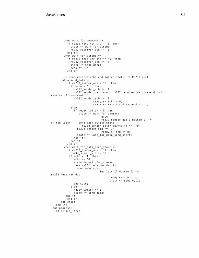
JavaCores !
63!
JavaCores Final Design Report
68
when wait_for_command => if rs232_receiver_stb = '1' then state <= wait_for_strobe; rs232_receiver_ack <= '1'; end if; when wait_for_strobe => if rs232_receiver_stb <= '0' then rs232_receiver_ack <= '0'; state <= send_data; echo <= '1'; end if; -- send reverse echo and switch states to RS232 port when send_data => if rs232_sender_ack = '0' then if echo = '1' then rs232_sender_stb <= '1'; rs232_sender_dat <= not rs232_receiver_dat; --send back reverse of char sent in rs232_sender_stb <= '1'; ready_switch <= 0; state <= wait_for_data_send_start; else if ready_switch = 0 then state <= wait_for_command; else rs232_sender_dat(3 downto 0) <= switch_latch ; --send back switch state rs232_sender_dat(7 downto 4) <= x"0"; rs232_sender_stb <= '1'; ready_switch <= 0; state <= wait_for_data_send_start; end if; end if; end if; when wait_for_data_send_start => if rs232_sender_ack = '1' then rs232_sender_stb <= '0'; if echo = '1' then echo <= '0'; state <= wait_for_command; case rs232_receiver_dat is when others => led_latch(7 downto 0) <= rs232_receiver_dat; ready_switch <= 1; state <= send_data; end case; else ready_switch <= 0; state <= send_data; end if; end if; end case; end if; end process; led <= led_latch;
JavaCores !
64!
JavaCores Final Design Report
69
end architecture rtl;
rs232receiver.vhd -- Copyright (c) 2006 Frank Buss ([email protected]) -- See license.txt for license -- -- RS232 receiver with Wishbone master interface and fixed, but generic, -- baudrate and 8N1 mode. -- -- This master sets stb_o to 1, after one byte was received and before the -- stop is received. When the slave acknowledges the strobe with ack_i = 1, -- stb_o is reset to 0. -- -- Supported Whishbone cycles: MASTER, WRITE library IEEE; use IEEE.STD_LOGIC_1164.ALL; use IEEE.NUMERIC_STD.ALL; use IEEE.MATH_REAL.ALL; entity rs232_receiver is generic(system_speed, baudrate: integer); port( ack_i: in std_logic; clk_i: in std_logic; dat_o: out unsigned(7 downto 0); rst_i: in std_logic; stb_o: out std_logic; rx: in std_logic); end entity rs232_receiver; architecture rtl of rs232_receiver is constant max_counter: natural := system_speed / baudrate; type state_type is ( wait_for_rx_start, wait_half_bit, receive_bits, wait_for_stop_bit); signal state: state_type := wait_for_rx_start; signal baudrate_counter: natural range 0 to max_counter := 0; signal bit_counter: natural range 0 to 7 := 0; signal shift_register: unsigned(7 downto 0) := (others => '0'); begin update: process(clk_i, ack_i) begin if rising_edge(clk_i) then if rst_i = '1' then state <= wait_for_rx_start; dat_o <= (others => '0'); stb_o <= '0'; else case state is when wait_for_rx_start => if rx = '0' then
JavaCores !
65!
JavaCores Final Design Report
70
-- start bit received, wait for a half bit time -- to sample bits in the middle of the signal state <= wait_half_bit; baudrate_counter <= max_counter / 2 - 1; end if; when wait_half_bit => if baudrate_counter = 0 then -- now we are in the middle of the start bit, -- wait a full bit for the middle of the first bit state <= receive_bits; bit_counter <= 7; baudrate_counter <= max_counter - 1; else baudrate_counter <= baudrate_counter - 1; end if; when receive_bits => -- sample a bit if baudrate_counter = 0 then shift_register <= rx & shift_register(7 downto 1); if bit_counter = 0 then state <= wait_for_stop_bit; else bit_counter <= bit_counter - 1; end if; baudrate_counter <= max_counter - 1; else baudrate_counter <= baudrate_counter - 1; end if; when wait_for_stop_bit => -- wait for the middle of the stop bit if baudrate_counter = 0 then state <= wait_for_rx_start; if rx = '1' then dat_o <= shift_register; stb_o <= '1'; -- else: missing stop bit, ignore end if; else baudrate_counter <= baudrate_counter - 1; end if; end case; end if; end if; -- when acknowledged, reset strobe if ack_i = '1' then stb_o <= '0'; end if; end process; end architecture rtl;
rs232sender.vhd -- Copyright (c) 2006 Frank Buss ([email protected]) -- See license.txt for license -- -- RS232 receiver with Wishbone master interface and fixed, but generic,
JavaCores !
66!
JavaCores Final Design Report
71
-- baudrate and 8N1 mode. -- -- This master sets stb_o to 1, after one byte was received and before the -- stop is received. When the slave acknowledges the strobe with ack=1, -- stb_o is reset to 0. -- -- Supported Whishbone cycles: MASTER, WRITE library IEEE; use IEEE.STD_LOGIC_1164.ALL; use IEEE.NUMERIC_STD.ALL; use IEEE.MATH_REAL.ALL; entity rs232_receiver is generic(system_speed, baudrate: integer); port( ack_i: in std_logic; clk_i: in std_logic; dat_o: out unsigned(7 downto 0); rst_i: in std_logic; stb_o: out std_logic; rx: in std_logic); end entity rs232_receiver; architecture rtl of rs232_receiver is constant max_counter: natural := system_speed / baudrate; type state_type is ( wait_for_rx_start, wait_half_bit, receive_bits, wait_for_stop_bit); signal state: state_type := wait_for_rx_start; signal baudrate_counter: natural range 0 to max_counter := 0; signal bit_counter: natural range 0 to 7 := 0; signal shift_register: unsigned(7 downto 0) := (others => '0'); begin update: process(clk_i, ack_i) begin if rising_edge(clk_i) then if rst_i = '1' then state <= wait_for_rx_start; dat_o <= (others => '0'); stb_o <= '0'; else case state is when wait_for_rx_start => if rx = '0' then -- start bit received, wait for a half bit time -- to sample bits in the middle of the signal state <= wait_half_bit; baudrate_counter <= max_counter / 2 - 1; end if; when wait_half_bit => if baudrate_counter = 0 then
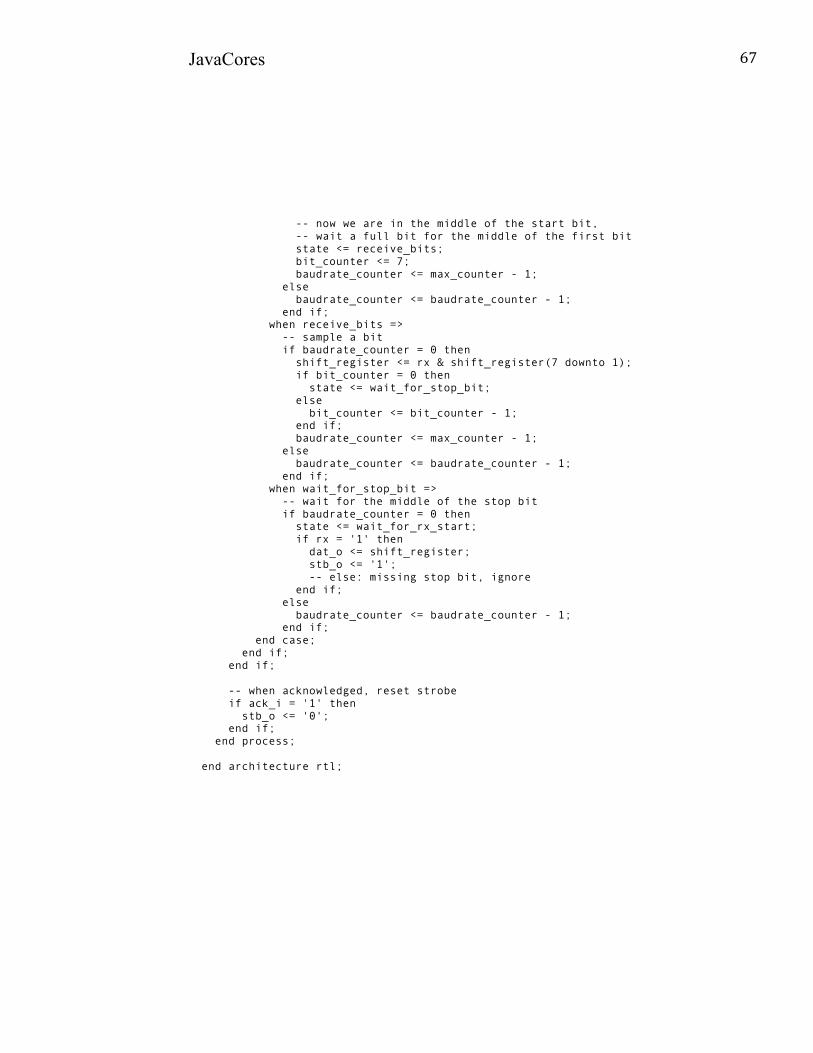
JavaCores !
67!
JavaCores Final Design Report
72
-- now we are in the middle of the start bit, -- wait a full bit for the middle of the first bit state <= receive_bits; bit_counter <= 7; baudrate_counter <= max_counter - 1; else baudrate_counter <= baudrate_counter - 1; end if; when receive_bits => -- sample a bit if baudrate_counter = 0 then shift_register <= rx & shift_register(7 downto 1); if bit_counter = 0 then state <= wait_for_stop_bit; else bit_counter <= bit_counter - 1; end if; baudrate_counter <= max_counter - 1; else baudrate_counter <= baudrate_counter - 1; end if; when wait_for_stop_bit => -- wait for the middle of the stop bit if baudrate_counter = 0 then state <= wait_for_rx_start; if rx = '1' then dat_o <= shift_register; stb_o <= '1'; -- else: missing stop bit, ignore end if; else baudrate_counter <= baudrate_counter - 1; end if; end case; end if; end if; -- when acknowledged, reset strobe if ack_i = '1' then stb_o <= '0'; end if; end process; end architecture rtl;
JavaCores !
68!
PLANES 2.1 LIST OF PLANES
A- Schematic PANDA XPRESSO
A PANDABOARD MEZZANINE CARD
Function Sheet Number
Block Diagram 2 Panda Header, USB 3 FPGA Banks 1 and 3 4
FPGA Banks 0,2, 101 and 123
5
FPGA Flash and JTAG 6 FPGA Decoupling 7
DDR3 8 DACs and ADCs 9
Display 10 Switches, LEDs, RS-232 11
Power 12 Headers 13
B- Layout
Function Page Number
Panda Xpresso 3D Design 83
Top Copper 84
Inner Layer I 84
Inner Layer II (Power) 85
Inner Layer III (Ground) 85
Inner Layer IV 86
Inner Layer V 86
Inner Layer VI 87
Bottom Copper 87
JavaCores !
69!
Top Silk 88
Bottom Silk 88
Drill Plot 89
Top Solder Mask 89
Bottom Solder Mask 90
2.2 PLANES
A- Schematic The design of the Panda Xpresso schematics has been primarily based on two reference
schematics, the Avnet Spartan 6 LX150T Development Board by Xilinx and the
PandaDAQ by Mark Haun, which can correspondingly be found at
http://www.em/avnet.com and
http://www.keteu.org/~haunma/proj/pandadaq/pandadaq_schem.pdf.
The thirteen page schematic has been created using Proteus PCB Design (ISIS). The
component’s election has been based on price and performance, and each of the
components’ symbols, pin outs assignment, and connections have been carefully
verified.
JavaCores !
70!
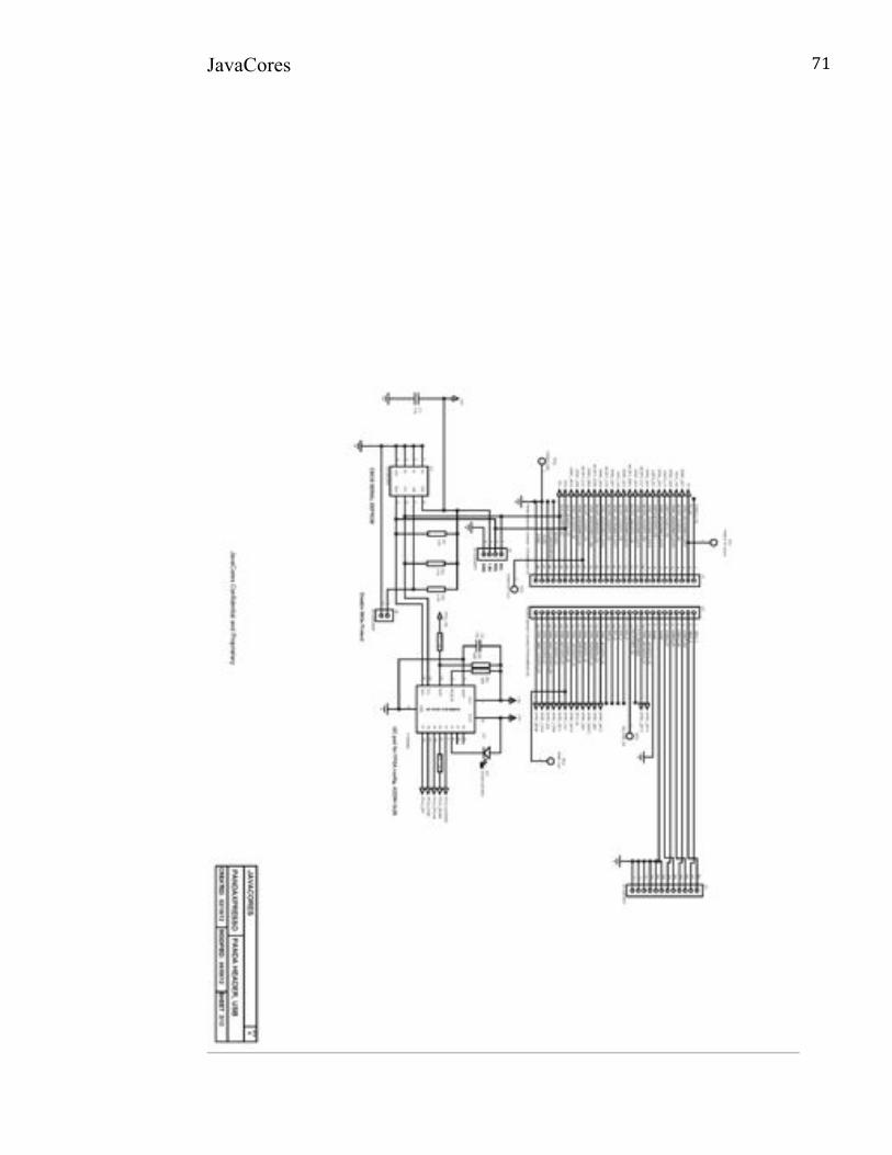
JavaCores !
71!
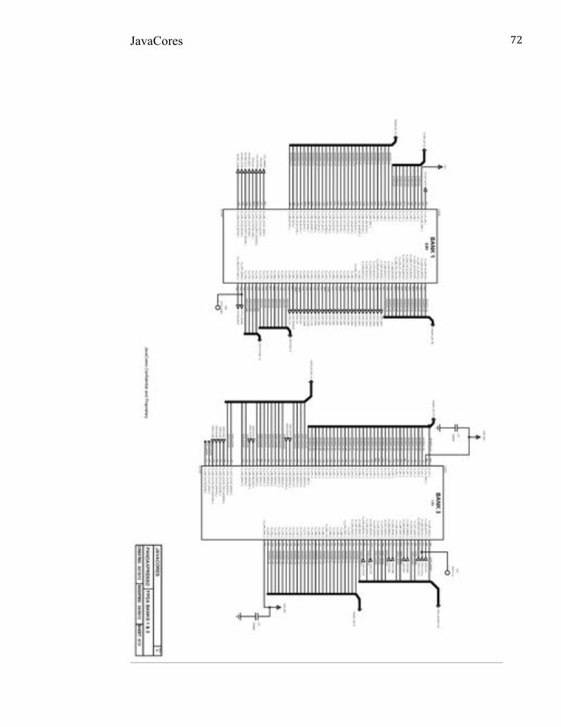
JavaCores !
72!
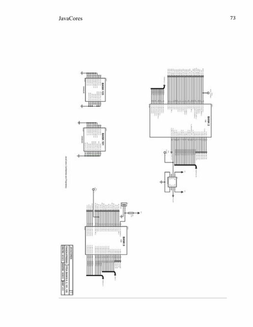
JavaCores !
73!

JavaCores !
74!
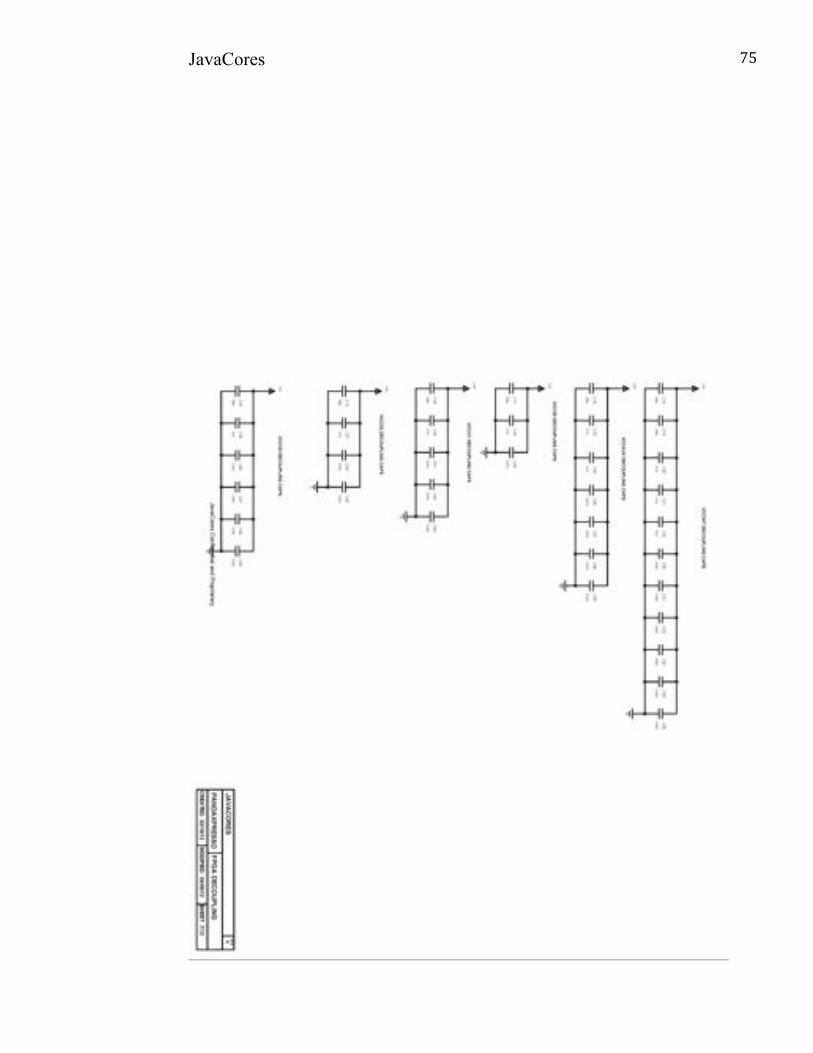
JavaCores !
75!
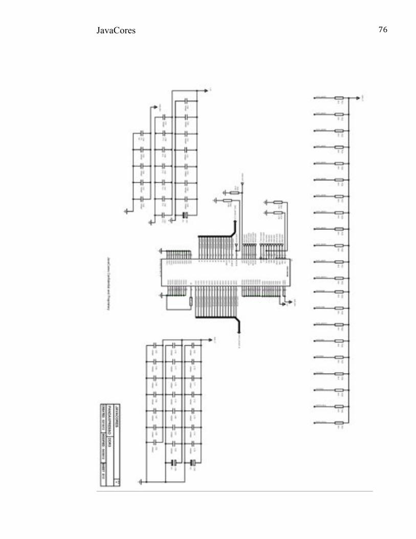
JavaCores !
76!
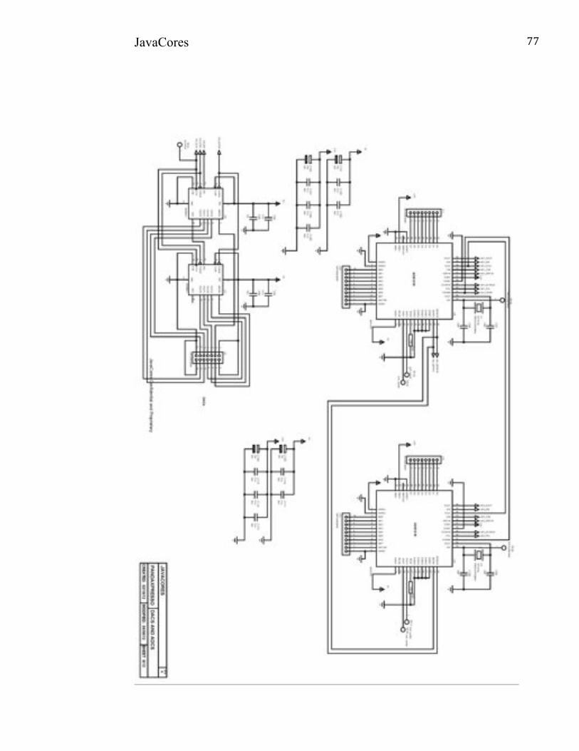
JavaCores !
77!
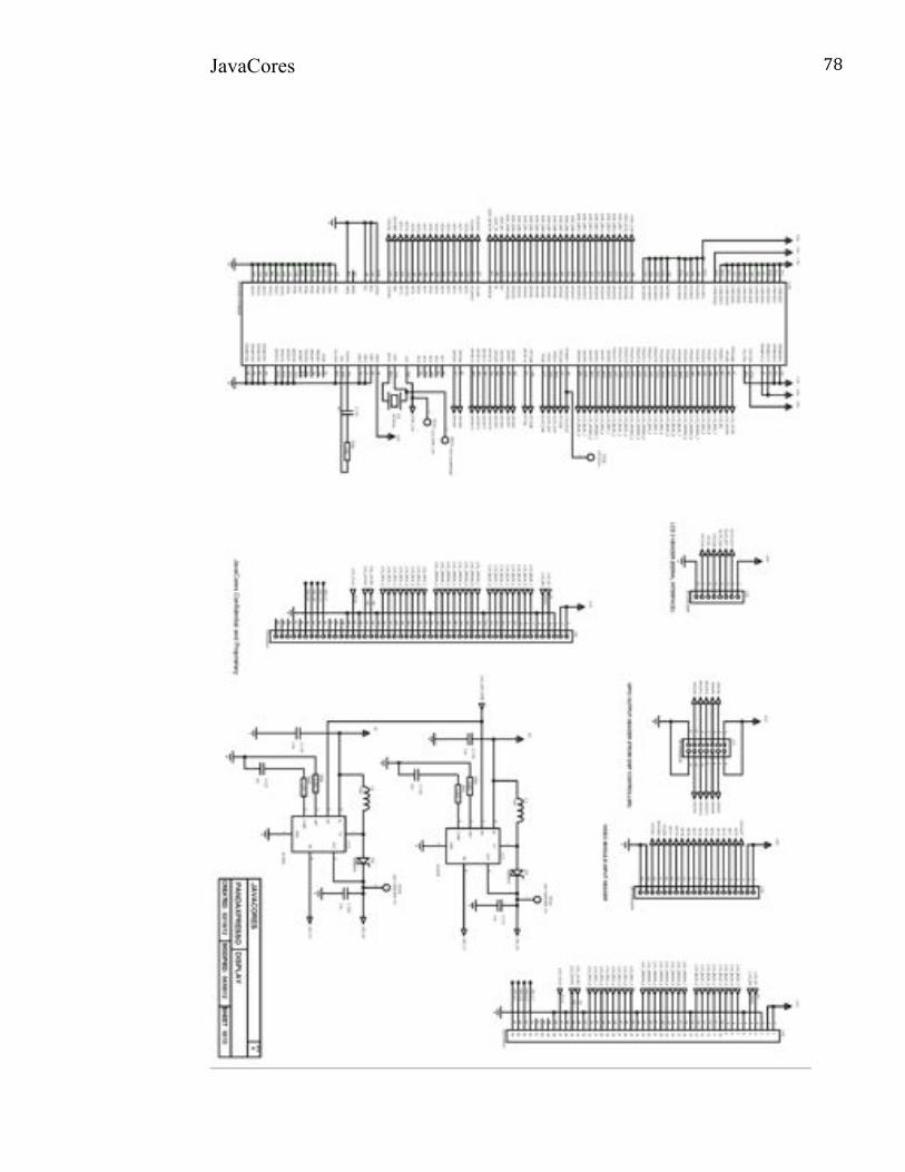
JavaCores !
78!
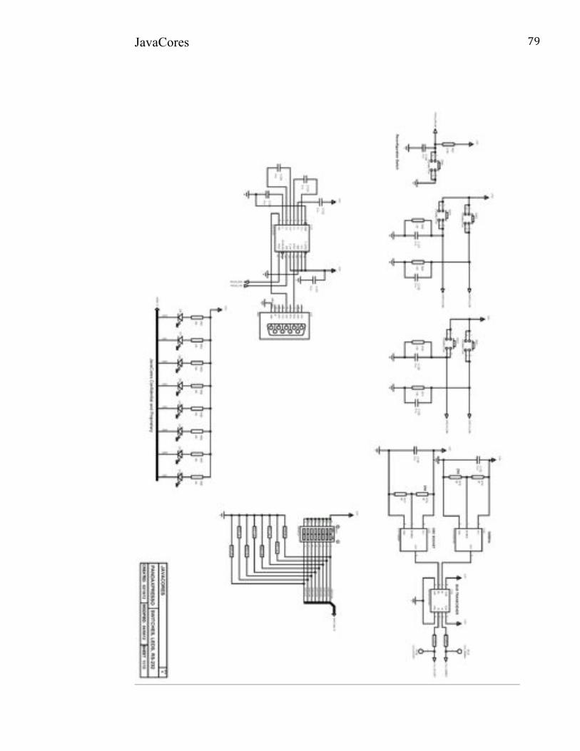
JavaCores !
79!
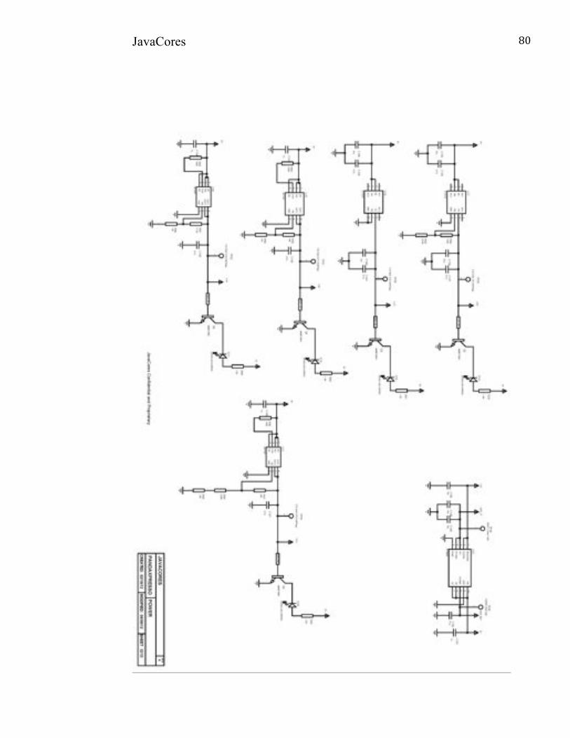
JavaCores !
80!
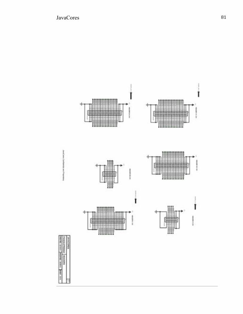
JavaCores !
81!
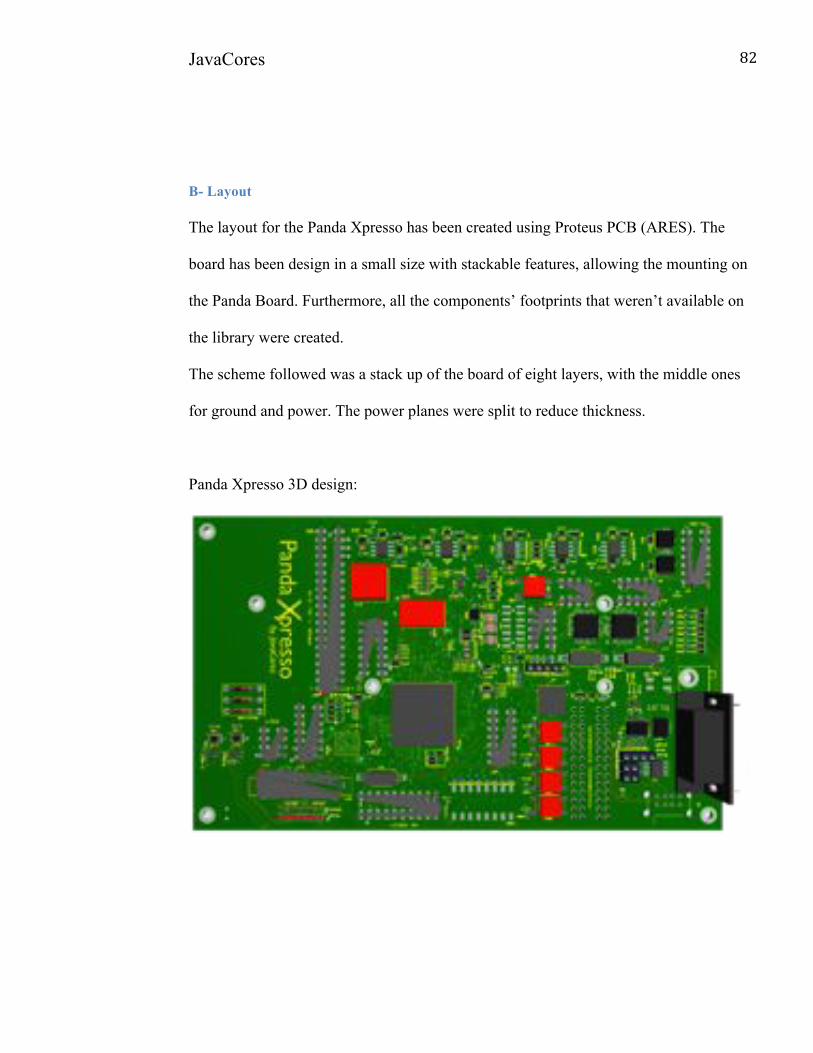
JavaCores !
82!
B- Layout The layout for the Panda Xpresso has been created using Proteus PCB (ARES). The
board has been design in a small size with stackable features, allowing the mounting on
the Panda Board. Furthermore, all the components’ footprints that weren’t available on
the library were created.
The scheme followed was a stack up of the board of eight layers, with the middle ones
for ground and power. The power planes were split to reduce thickness.
Panda Xpresso 3D design:
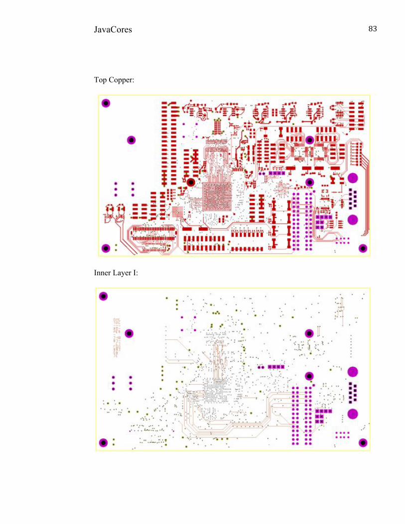
JavaCores !
83!
Top Copper:
Inner Layer I:
JavaCores Final Design Report
47
Layout
Top Copper
Inner Layer 1
JavaCores Final Design Report
47
Layout
Top Copper
Inner Layer 1
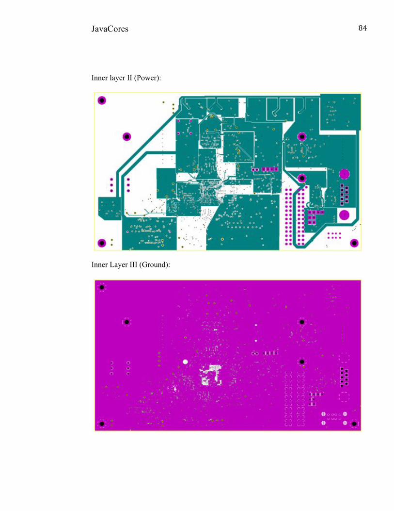
JavaCores !
84!
Inner layer II (Power):
Inner Layer III (Ground):
JavaCores Final Design Report
48
Inner Layer 2 (Power)
Inner Layer 3 (Ground)
JavaCores Final Design Report
48
Inner Layer 2 (Power)
Inner Layer 3 (Ground)
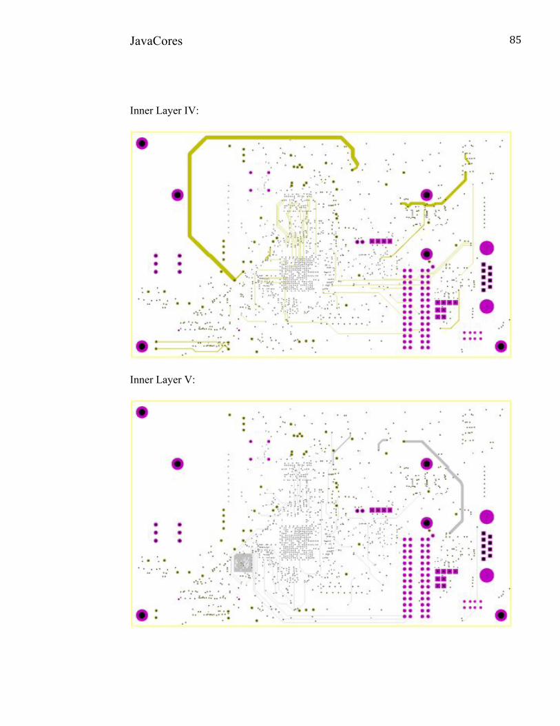
JavaCores !
85!
Inner Layer IV:
Inner Layer V:
JavaCores Final Design Report
49
Inner 4
Inner 5
JavaCores Final Design Report
49
Inner 4
Inner 5
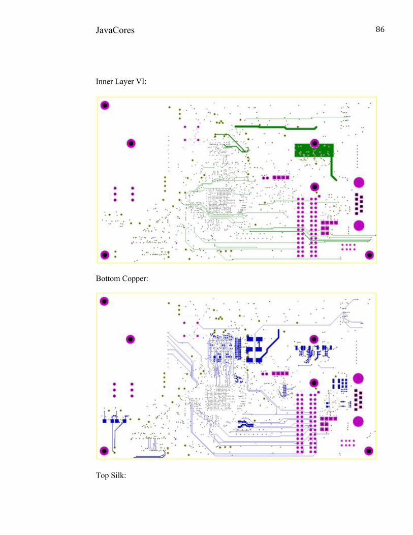
JavaCores !
86!
Inner Layer VI:
Bottom Copper:
Top Silk:
JavaCores Final Design Report
50
Inner 6
Bottom Copper
JavaCores Final Design Report
50
Inner 6
Bottom Copper
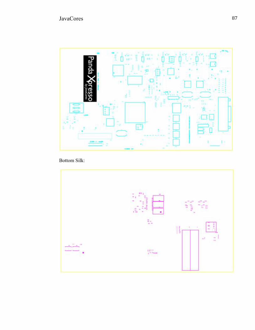
JavaCores !
87!
Bottom Silk:
JavaCores Final Design Report
49
Top Silk
Bottom Silk
JavaCores Final Design Report
49
Top Silk
Bottom Silk
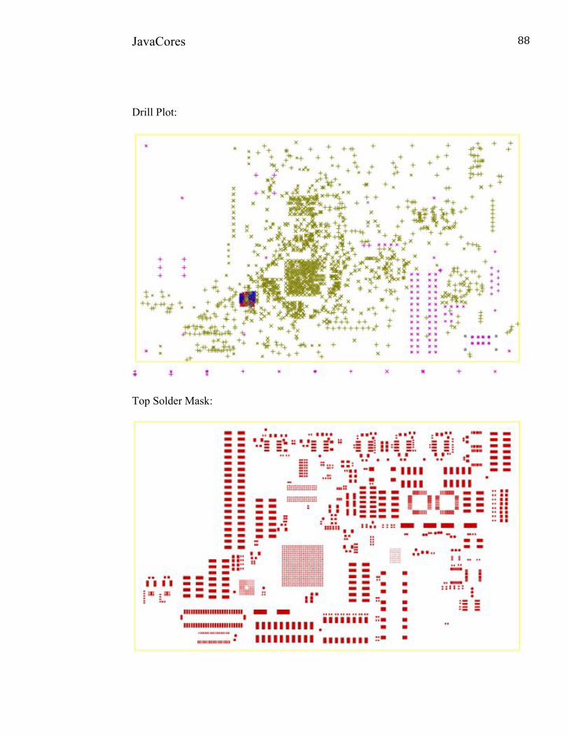
JavaCores !
88!
Drill Plot:
Top Solder Mask:
JavaCores Final Design Report
50
Drill Plot
Top Solder Mask
JavaCores Final Design Report
50
Drill Plot
Top Solder Mask
JavaCores !
89!
Bottom Solder Mask:
JavaCores Final Design Report
51
Bottom Solder Mask
JavaCores !
90!
PROJECT PLAN 3.1$GENERAL$AND$ECONOMIC$PROJECT$PLAN$The microprocessor XC-110 datasheet is not included in this document, due to
confidentiality reasons. Arrangements to view the document can be arranged under a
Non-Disclosure Agreement.
The codes and standards that apply to this specific project are related to the following:
• Institute of Electrical and Electronics Engineers (IEEE) (IEEE-SA, 2010)
• Java™ Version 2, Micro Edition (J2ME), licensed under the General Public
License and released under the project name phoneme (Oracle)
• Java™ Runtime Environment (JRE)
• Java™ application programming interfaces (APIs), which any Java™ Virtual
Machine (JVM) will use (Oracle, 2011)
• Connected Limited Device Configuration (CLDC), which provides the most
basic set of libraries and features that must be present in each implementation of
a J2ME environment (Wireless Center)
• ARM Advanced Microcontroller Bus Architecture (AMBA) (ARM, 2011)
o The AMBA 4.0 specification defines five buses/interfaces:
! Advanced extensible Interface (AXI)
! Advanced High-Performance Bus (AHB)
! Advanced System Bus (ASB)
! Advanced Peripheral Bus (APB)
! Advanced Trace Bus (ATB).

JavaCores !
91!
• The Secure Digital Standard-capacity (SDSC) (SD Association, 2011)
• Universal Serial Bus (USB) (USB Implementers Forum, Inc.)
• mLAN (mobile Local Area Network) (IEEE 802.11a/b/g/n)
• Bluetooth 3.0
3.2 TECHNICAL AND PARTICULAR PROJECT PLAN
3.2.1 FABRICATION A majority of the fabrication for this project was handled by outside vendors. Once the
schematic and layout of the board were finished, the board was sent to Accutrace Inc. for
manufacturing. Accutrace, Inc. manufactured ten boards, although only one board was
populated. The board was manually populated except for the BGAs. Qsic worked on the
BGAs, while the rest of the components including, resistors, capacitors, and ICs were
installed manually. For the populations the appropriate tools and equipment provided by
University of San Diego were used.
3.2.2 TESTING After the boards were manufactured, Accutrace Inc. performed an electrical test on each
individual board. The device under testing phase did undergo tests to verify the
functionality of the FPGA as well as the interaction between the Panda Xpresso and the
PandaBoard through the I2C interface.
Furthermore, In order to test the software that will be used on board, the PandaBoard
was directly connected to the Spartan 3A Development Kit, which acted as the Panda
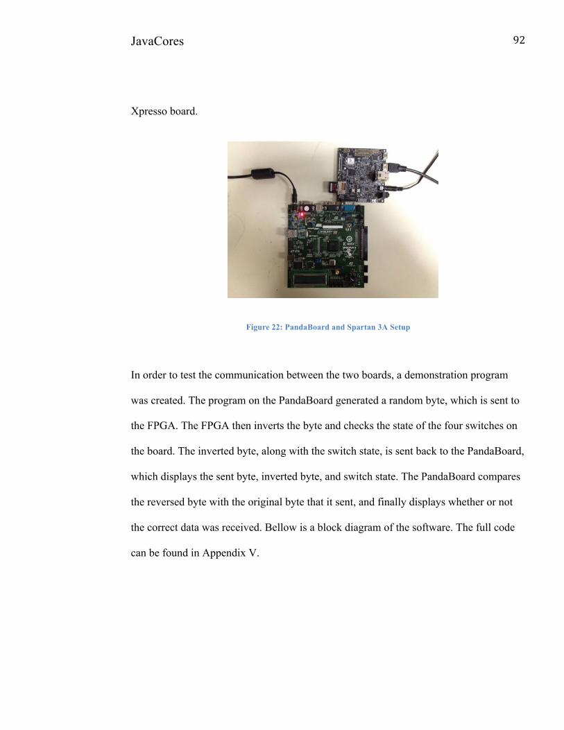
JavaCores !
92!
Xpresso board.
Figure 22: PandaBoard and Spartan 3A Setup
In order to test the communication between the two boards, a demonstration program
was created. The program on the PandaBoard generated a random byte, which is sent to
the FPGA. The FPGA then inverts the byte and checks the state of the four switches on
the board. The inverted byte, along with the switch state, is sent back to the PandaBoard,
which displays the sent byte, inverted byte, and switch state. The PandaBoard compares
the reversed byte with the original byte that it sent, and finally displays whether or not
the correct data was received. Bellow is a block diagram of the software. The full code
can be found in Appendix V.
JavaCores Final Design Report
20
communication between the Panda Xpresso and PandaBoard. This involved writing a VHDL code and a program written in C that uploads the VHDL bitfile directly to the Panda Xpresso from the PandaBoard. The VHDL code was written in Xilinx ISE 13.4 and includes a UCF of the entire Panda Xpresso FPGA, as well as a small verification program.
Project Plan
Fabrication A majority of the fabrication for this project was handled by outside vendors. Once the schematic and layout of the board were finished, the board was sent to Accutrace, Inc for manufacturing. Accutrace, Inc. manufactured ten boards, although only one board was populated. The board was populated by our industry mentor and by the team. The BGAs were installed by our industry mentor because of his access to the appropriate tools, and the remainder of the components on the board was populated by the team using equipment provided by University of San Diego.
Testing After the boards were manufactured, Accutrace Inc. performed an electrical test on each individual board. The device is currently in testing phase, and will undergo tests to verify the functionality of the FPGA as well as the interaction between the Panda Xpresso and the PandaBoard through the I2C interface. In order to test the software developed by the team that will be used on board, the PandaBoard was directly connected to the Spartan 3A Development Kit, which acted as the Panda Xpresso board, as shown in Figure below.
Figure 8: PandaBoard and Spartan 3A Test Setup

JavaCores !
93!
Figure 23: Software Block Diagram
3.2.3 PROJECT DELIVERABLES The deliverables for the project consisted of an entirely functional platform, as well as
VHDL code that allows the Panda Xpresso to communicate with the PandaBoard. In
order to create the Panda Xpresso PCB, the schematic was created using Proteus, which
was provided by the industry mentor, Bob Ganton. The PCB is the project’s overall
deliverable and this has been manufactured, populated, and tested using the new
developed software.
• Processors: The host processor used in this design (acting as a processor
in a modern day smart phone) is a TI OMAP4 Processor. This processor
has been mounted on a PandaBoard.
• Programming Host Platform: A bootstrap and Ubuntu 12.04 have been
loaded onto an SD card, which has successfully booted the PandaBoard.
JavaCores Final Design Report
21
In order to test the communication between the two boards, a demonstration program was created. The program on the PandaBoard generates a random byte, which is sent to the FPGA. The FPGA then inverts the byte and checks the state of the four switches on the board. The inverted byte, along with the switch state, is sent back to the PandaBoard, which displays the sent byte, inverted byte, and switch state. The PandaBoard compares the reversed byte with the original byte that it sent and displays whether or not the correct data was received. Below is a block diagram of the software. The full code can be found in Appendix G.
STARTSend(Binary(Byte(
from(PandaBoard(to(FPGA
Display(Byte(Sent Invert(Byte(using(FPGA
Get(Switch(State(from(FPGA
Display(Inverted(ByteDisplay(Switch(StateIs(value(equal(to(
FF?
Display(FAILURE!
Display(SUCCESS!New(LineCompare(Sent(Byte(
with(Inverted(Received(Byte
No
Yes
Send(Switch(state(and(inverted(byte(to(
PandaBoard
Figure 9: Software Test Block Diagram
Project Deliverables The deliverables for the project consisted of an entirely functional platform, as well as VHDL code that allows the Panda Xpresso to communicate with the PandaBoard. In order to create the Panda Xpresso PCB, we first created the schematic using Proteus, which was provided to us by our industry mentor, Bob Ganton. The PCB is the team’s overall deliverable and this has been manufactured, populated, and tested using the software developed by the team.
• Processors: The host processor used in this design (acting as a processor in a modern day smart phone) is a TI OMAP4 Processor. This processor has been mounted on a PandaBoard.
• Programming Host Platform: We have loaded a bootstrap and Ubuntu 12.04 onto an SD card, which has successfully booted the PandaBoard.
JavaCores !
94!
This permits that while optimizing the design for running Ubuntu,
Android™ and Gingerbread™ can still be running.
• Programming of FPGA: The FPGA was programmed using VHDL.
• Programming Medium: The VHDL developed was created in Xilinx
13.4 ISE.
• Special Design Medium: The schematic and layout design for the PCB
was completed with Proteus PCB Design Software. A copy of the
software was provided by Bob Ganton. Also, Linux/Ubuntu 12.04 was
used throughout the design process.
• Other Components: The proposed LCD is a 4.3” WVGA LED TFT-
LCD. Additionally, SDRAM from Micron is used for the host processor’s
memory. This memory is 1Gx16, 200MHz, manufacturer part number
(MPN) MT46H64M16LFBF-5IT:B.
3.2.4 FINAL DELIVERABLE The manufacturer Accutrace Inc. produced a total of ten Panda Xpresso boards.
Nevertheless, only one of them was entirely populated. The population process was
developed in two stages: BGAs’ installation and the manually population of the rest of
the components. The BGAs were installed by the company Qsic, while the rest of the
components were populated by hand at the University of San Diego’s lab Loma 209.
The implementation of the VHDL program wasn’t accomplished due to compatibilities
issues of the Spartan 6 LTX150 and the available Xilinx Software license. Nevertheless,
JavaCores !
95!
the Panda Xpresso board was successfully powered and all the voltages were
successfully tested. Moreover, the Xilinx software recognized the FPGA and the
platform flash.
A demonstration using the Spartan 3A Development Kit has being carried to show how
the Spartan 6 LX150 can potentially perform. The Spartan 3 board is used as a
substitute demonstration platform, which runs the same code from the PandaBoard to the
Spartan 3A and vice versa, that the Panda Xpresso would run. By demonstrating the
interaction between the Spartan 3A FPGA and the PandaBoard, which communicate via
I2C and SPI, proved that the software to be implemented onto the Panda Xpresso is
valid.
3.2.5 SCHEDULE The schedule of the project has drastically changed from the original due to the design
change request from JavaCores. First semester, a majority of the time was spent
researching and exploring the files provided by JavaCores that would essentially build
the XC-110. Near the end of the first semester, however, the code was not ready to be
executed and thus, it would need drastic professional modification. Therefore, work on
the newly designed Panda Xpresso board did not begin until second semester. This
caused many major setbacks in the initial schedule. The schematic design and layout
consumed eight weeks of work. This was largely due to the learning curve associated
with Proteus PCB Design, as well as the research that needed to be completed for each
component used. The routing took an additional two weeks, there were over 2100 nets to
JavaCores !
96!
route. To get the board sent out to manufacturers also took an extra week because of last
minute changes that were required before the board could be produced. Overall, the PCB
design consumed the most amount of time of the project and this called for many
adjustments to the schedule. Only a small amount of time was left for the population of
the board, which was done directly after the PCB returned from manufacturing. The
estimated time of population was of two days. Nevertheless, as a back up plan in case of
delays in the manufacturing/populating processes, a small simulation that emulates the
environment of the PandaBoard and Panda Xpresso was assembled. This is discussed
below in Predicted Results.
However, as with any engineering design project, there are unforeseeable outcomes that
have the ability to cause major delay. The schedule has been adjusted accordingly
because of these major delays.
BUDGET 4.1 BILL OF MATERIALS The following table gathers each of the components’ information including: Type of
component, Reference, Order Code (on DigiKey or Mouser), Price and Quantity (for one
table).
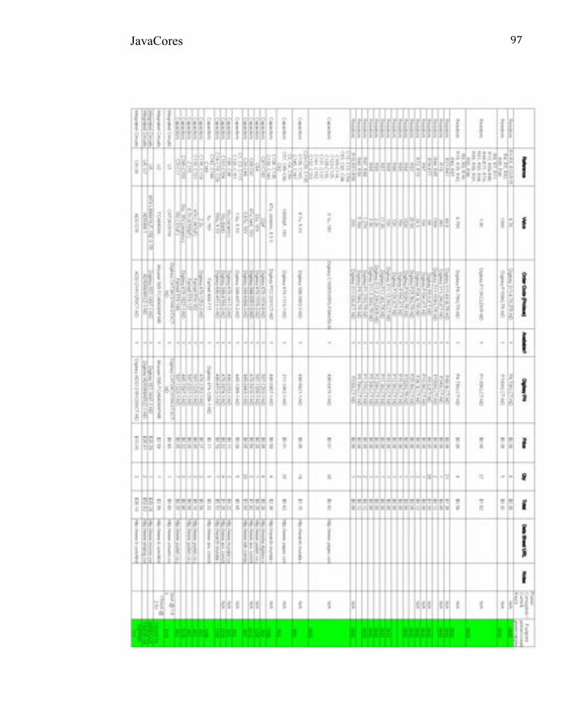
JavaCores !
97!
JavaCores Final Design Report
52
Appendix F: Bill of Materials
JavaCores !
98!
JavaCores Final Design Report
53

JavaCores !
99!
JavaCores Final Design Report
54
JavaCores !
100!
4.2 GENERAL BUDGET The general budget for this project is described in detail below:
Table 4: General Budget Part/Material Supplier Cost Quantity Subtotal
Spartan 6 XC6SLX150T DigiKey $197.50 1 $197.50
TFT LCD WVGA
screen
DigiKey $100.70 1 $100.70
PandaBoard DigiKey $187.00 1 $187.00
PCB Manufacturing Accutrace,
Inc.
$1650.00 1 $1650.00
Additional PCB
components
DigiKey
Mouser
$553.88 1 $553.88
Total $2689.08
Final BOM (Bill Of Materials) total: $434.18
Final BOM excluding FPGA and LCD: $236.68
PCB components Total: $553.88
• Including passive components for five boards
• Including one IC’s for one board
• Including shipping cost
PCB manufacturing total cost: $1650.00
• A total of ten boards were manufactured by Accutrace Incorporated