Embed Size (px)
Citation preview
Exploring DC/DC Converters with PowerESIM:
A Laboratory Manual
Siew-Chong Tan, Chi Kong Tse, Yuk Ming Lai Circuits and Microelectronics Section
Department of Electronic and Information Engineering The Hong Kong Polytechnic University
Hung Hom, Kowloon, Hong Kong
Frankie Poon and Joe Liu, PowerELab Limited
1/F Technology Innovation and Incubation Building Hong Kong University, Pokfulam Road, Hong Kong
08 May 2007

II
Copyright © 2007 by Siew-Chong Tan, Chi Kong Tse, Yuk Ming Lai, Frankie Poon, and Joe Liu. All rights reserved. No part of this publication may be reproduced, stored in a retrieval system, or transmitted, in any form or by any means, electronic, mechanical, photocopying, recording, or otherwise, without prior permission of the author.

III
Preface
This laboratory manual is originally developed for an introductory power electronics course in the Department of Electronic and Information Engineering, Hong Kong Polytechnic University, Hong Kong. The labs are based on PowerESim, an internet-based computer aided design (CAD) software tool for switch-mode power supplies developed by the PowerELab Limited. The general aim of the labs is to provide students essential knowledge and practical design experience on the development of DC-DC switch-mode power supplies. The exercises have been designed for senior students who have selected this elective coursework in their Bachelor/Master Degree of Electronic and Information Engineering programme. Most experiments in the manual are software based, which requires only the personal computers and broadband internet access, and are therefore highly appropriate for large classes. With simple and easy to follow procedures in each of the laboratory exercises, students require only minimal supervision when performing the labs. Each of the laboratory exercises (software) can be completed within a three-hour laboratory session. An optional hardware exercise, which requires about 15 hours work time, is also included in Laboratory 4 as a hands-on exercise for students. So far, we have had some successes in communicating the necessary knowledge to students through these laboratory sessions. We will be pleased to receive comments and suggestions from instructors who would use these labs in their training. Utilization of PowerESim in Course Agenda There will be four laboratory sessions in this course. The learning objectives of these sessions can be briefly described as follows. • Laboratory 1 is to familiarize the students with the operation and features of the
PowerESim software. • Laboratory 2 is for students to investigate the static and dynamic properties of the buck
and boost converters, and their feedback circuits, with respect to variations of circuit parameters, using existing converter platforms in the PowerESim package.
• Laboratory 3 is for students to investigate on how different parameters (physical dimensions, windings, core choices) can affect the magnetic properties of inductors and transformers, using the Magnetic Builders toolbox in the PowerESim package.
• Laboratory 4 is for students to experience the process of designing a practical power supply design, using the design framework and analytical toolboxes provided in the PowerESim package.
Acknowledgement The material in this tutorial is developed in corporation with PowerELab Limited.

IV
Table of Contents
Preface …………………………………………………………………………………….....III Utilization of PowerESim in Course Agenda ……………………………………..…………III Acknowledgement …………………………………………………………………………...III Table of Contents ……………………………………………………………………………IV List of Figures ……………………………………………………………………………….VI List of Tables ...…………………………………………………………………………….VIII Laboratory 1: Introduction to PowerESim 1.1 Objectives ……………………………………………………………………………..1 1.2 Introduction …………………………………………………………………………...1 1.3 Features/Operations of the PowerESim Package ……………………………………..1 1.4 Login Procedures ……………………………………………………………………...3 1.5 Exercises ……………………………………………………………………………....3 1.5.1 Exercise 1 ……………………………………………………………………..3 1.5.2 Exercise 2 ……………………………………………………………………..7 1.5.3 Exercise 3 ……………………………………………………………………..8
1.5.4 Exercise 4 ……………………………………………………………………12 1.5.5 Exercise 5 ……………………………………………………………………14 1.5.6 Exercise 6 ……………………………………………………………………15 1.5.7 Exercise 7 ……………………………………………………………………17 1.5.8 Exercise 8 ……………………………………………………………………19 1.5.9 Exercise 9 ……………………………………………………………………20 1.5.10 Exercise 10…………………………………………………………………...21
1.6 Assignment …………………………………………………………………………..22 Laboratory 2: Understanding the Characteristics of Buck and Boost Converters and Their
Control 2.1 Objectives …………………………………………………………………………....23 2.2 Introduction ………………………………………………………………………….23 2.2.1 Buck Converter ……………………………………………………………... 23 2.2.2 Boost Converter ……………………………………………………………...24 2.2.3 Controller …………………………………………………………………….25 2.2.4 Storage Elements …………………………………………………………….26 2.3 Exercises ……………………………………………………………………………..27 2.3.1 Exercise 1 ……………………………………………………………………27 2.3.2 Exercise 2 ……………………………………………………………………30 2.3.3 Exercise 3 ……………………………………………………………………34 2.3.4 Exercise 4 ……………………………………………………………………35 2.3.5 Exercise 5 ……………………………………………………………………38 2.3.6 Exercise 6 ……………………………………………………………………40 2.4 Assignment …………………………………………………………………………..42 2.5 References …………………………………………………………………………...42
V
Laboratory 3: Properties of Magnetic Devices 3.1 Objectives …………………………………………………………………………....43 3.2 Introduction ………………………………………………………………………….43 3.2.1 Common Types of magnetic Core Shapes ………………………………….43 3.2.2 General Terminologies of Magnetic Core …………………………………...44 3.2.3 Bobbins ………………………………………………………………………45 3.2.4 Practical Magnetic Devices ………………………………………………….45 3.3 Exercises ……………………………………………………………………………..46 3.3.1 Exercise 1 ……………………………………………………………………46 3.3.2 Exercise 2 ……………………………………………………………………48 3.3.3 Exercise 3 ……………………………………………………………………50 3.4 Assignment …………………………………………………………………………..51 Laboratory 4: Design and Construction of a 50 W Flyback Converter 4.1 Objectives …………………………………………………………………………....52 4.2 Introduction ………………………………………………………………………….52 4.3 Task 1 ………………………………………………………………………………..53 4.3 Task 2 (Optional) ……...……………………………………………………………..53
VI
List of Figures
Figure 1.1: Analytical tools module. ……………………………………………………….....2 Figure 1.2: Builders module. ……………………………………………………………… …3 Figure 1.3: Buck DC-DC. ……………………………………………………………… …….4 Figure 1.4: Pop-up window of buck DC-DC. ………………………………………………...4 Figure 1.5: Detailed specification. ……………………………………………………………5 Figure 1.6: Refreshed screen. …………………………………………………………………6 Figure 1.7: C7 selection screen. ………………………………………………………………6 Figure 1.8: Loss analysis screen. ……………………………………………………………...7 Figure 1.9: D1 selection screen. ………………………………………………………………8 Figure 1.10: Thermal simulation platform. …………………………………………………...9 Figure 1.11: Completed placement of components. …………………………………………10 Figure 1.12: Vertical placement of components. ……………………………………………10 Figure 1.13: Thermal analysis layout. ……………………………………………………….11 Figure 1.14: Rotation of component. ………………………………………………………...11 Figure 1.15: Attaching component to heatsink. ……………………………………………..12 Figure 1.16: DVT report. ……………………………………………………………….……13 Figure 1.17: MTBF screen. ……………………………………………………………….…14 Figure 1.18: Overall system analysis. ……………………………………………………….14 Figure 1.19: Individual component analysis. ………………………………………………..15 Figure 1.20: Loop analysis screen. …………………………………………………………..16 Figure 1.21: Transient analysis platform. ……………………………………………………16 Figure 1.22: Sinusoidal loading waveform. …………………………………………………17 Figure 1.23: Harmonic testing results. ………………………………………………………18 Figure 1.24: Voltage and current waveforms of M1 and D1. ……………………………….18 Figure 1.25: Magnetic builder popup screen. ………………………………………………..19 Figure 1.26: Magnetic builder selection screen. ……………………………………………..19 Figure 1.27: Magnetic loss report. …………………………………………………………...20 Figure 1.28: BOM report. ……………………………………………………………….…..21 Figure 1.29: Component builder. …………………………………………………………...21 Figure 1.30: Resistor builder screen. ………………………………………………………...22 Figure 2.1: The buck and boost converters. …………………………………………………23 Figure 2.2: The “On” and “Off” states of the buck converter. ………………………………24 Figure 2.3: The “On” and “Off” states of the boost converter. ……………………………...24 Figure 2.4: Overview of voltage mode control and peak current mode control. ……………25 Figure 2.5: Schematic of feedback controller in proposed buck DC-DC converter. ………..27 Figure 2.6: Open-loop characteristic of proposed buck DC-DC converter. …………………28 Figure 2.7: Compensation table of proposed buck DC-DC converter. ……………………...31 Figure 2.8: Characteristic of the compensated buck converter with voltage mode control. ...31 Figure 2.9: Transient analysis of the compensated system. …………………………………32 Figure 2.10: Clock generator symbol. ……………………………………………………….33 Figure 2.11: Loop phase plot. ………………………………………………………………..34 Figure 2.12: Characteristic of the compensated buck converter with peak current mode control. ……………………………………………………………….………………………35 Figure 2.12: Open-loop characteristic of proposed boost DC-DC converter. ……………….36

VII
Figure2.13: Characteristic of the compensated boost converter with voltage mode control. ……………………………………………………………………………………….38 Figure 2.14: Load current waveform for the compensated boost converter. ………………..39 Figure 2.15: Transient response of the boost converter with voltage mode control. ………..39 Figure 2.16: Advance setting table. ………………………………………………………….40 Figure 2.17: Characteristic of the boost converter with peak current mode control. ………..41 Figure 2.18: Transient response of the boost converter with peak current mode control. …..41 Figure 3.1: Common Types of Magnetic Core Shape. ………………………………………44 Figure 3.2: Common Types of Bobbin. ……………………………………………………...45 Figure 3.3: Some Practical Magnetic Devices. ……………………………………………...45

VIII
List of Tables
Table 2.1: Parameters of controller for achieving open-loop buck converter. ………………28 Table 2.2: Parameters of controller for achieving open-loop boost converter. ……………...36 Table 3.1: Power loss of the inductor with different inductances. …………………………..48 Table 3.2: Power loss of the inductor when operated under different conditions. …………..49 Table 3.3: Power loss of the inductor for different bobbin thicknesses. …………………….50 Table 4.1: Specification of flyback converter. ………………………………………………53
1
Laboratory 1
Introduction to PowerESim
1.1 Objectives 1. To familiarize students with the basic operation and features of the PowerESim software. 2. To give students a hands-on trial on the various functionalities of the software. 1.2 Introduction PowerESIM is an internet based computer aided design (CAD) software tool for switch-mode power supplies. The framework of this software is developed using actual practical power supplies circuit models and technical design methodologies, and is governed by the consideration of real-life industrial requirements and regulations. This framework is supported by a database of information (i.e., parameters, specifications, cost, etc.) collected from existing components in the market. With the choice of automatic and manual design options, the package can be effectively employed by both experienced and inexperienced engineers for optimizing the design of power supplies in terms of cost, performance, practicality, reliability, and/or other specified requirements compatible to industrial applications. Additionally, with the inclusion of features like the automatic report/document generation and cost evaluation/calculation functionalities, the software has been intelligently designed to serve diverse groups of the power supply industry, which includes engineers, managers, component vendors, and trainees, in ways other than simply the design of power supplies. Hence, it is a useful tool for those working or intending to work in power supplies related industry, to master. Furthermore, in terms of academic training, the PowerESim package can serve as a virtual power supply platform for students in their quests for improving their understanding of power electronics and power supplies, as well as a quick approach to verifying their theoretical knowledge in the area. For this coursework, the PowerESim is mainly engaged for both the aforementioned purposes. 1.3 Features/Operations of the PowerESim Package The PowerESim comprises seven Analytical Tools and three Builders function blocks that can be individually employed to supply critical analyses and simplified guidelines, which are important and helpful for optimizing the design of power supplies. The design procedure starts with the designer choosing a converter topology among a library option of 32 converter topologies that are most commonly used in the industrial power supply applications. With that, designers can select the appropriate power supply specification (i.e., input/output voltage and power requirements etc.) to generate a preliminary set of components for the selected topology matching the desired specification. Using the various analytical and builder
2
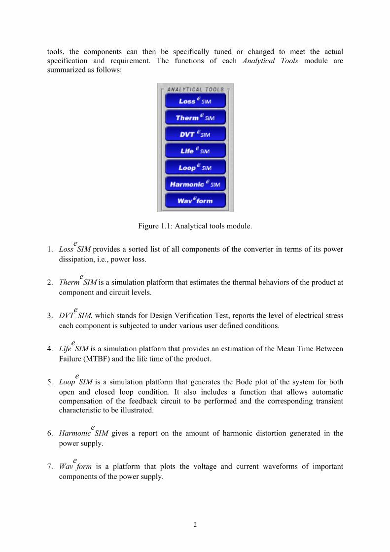
tools, the components can then be specifically tuned or changed to meet the actual specification and requirement. The functions of each Analytical Tools module are summarized as follows:
Figure 1.1: Analytical tools module.
1. LosseSIM provides a sorted list of all components of the converter in terms of its power
dissipation, i.e., power loss.
2. ThermeSIM is a simulation platform that estimates the thermal behaviors of the product at
component and circuit levels.
3. DVTeSIM, which stands for Design Verification Test, reports the level of electrical stress
each component is subjected to under various user defined conditions.
4. LifeeSIM is a simulation platform that provides an estimation of the Mean Time Between
Failure (MTBF) and the life time of the product.
5. LoopeSIM is a simulation platform that generates the Bode plot of the system for both
open and closed loop condition. It also includes a function that allows automatic compensation of the feedback circuit to be performed and the corresponding transient characteristic to be illustrated.
6. HarmoniceSIM gives a report on the amount of harmonic distortion generated in the
power supply.
7. Waveform is a platform that plots the voltage and current waveforms of important
components of the power supply.

3
The functions of the Builders modules are summarized as follows: 1. Magnetic Builder is a design platform for users to create their own magnetic components
by selecting different ferrite cores, bobbin (container) types, and the winding methods. 2. BOM Builder allows users to construct a report of the Bill of Material (BOM). 3. Component Builder provides a channel for users to model their preferred characteristics
of various electrical and electronic components commonly used in power supplies.
Figure 1.2: Builders module. With the aid of these functions, designers can easily generate an optimal power supply design in terms of circuit cost, efficiency, performance, and reliability, by selecting among different circuitries, components, design parameters, and manufacturers etc. 1.4 Login Procedure 1. The PowerESim is a licensed software that requires subscription. 2. Go to the website http://www.poweresim.com/. 3. Login using the username and password assigned to you. 4. You are now free to perform the following exercises. 1.5 Exercises 1.5.1 Exercise 1 This exercise aims to introduce the basic usage of PowerESim in the selection of converter topology and its components. 1. Log in using the Login Procedure described in the previous section. 2. Select the buck converter on the front page by first clicking Topologies and then double-
clicking on Buck DC-DC, as shown in Figure 1.3.
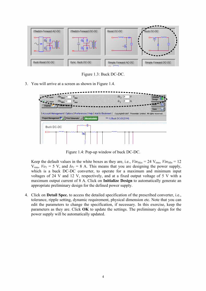
4
Figure 1.3: Buck DC-DC.
3. You will arrive at a screen as shown in Figure 1.4.
Figure 1.4: Pop-up window of buck DC-DC.
Keep the default values in the white boxes as they are, i.e., VinMax = 24 Vrms, VinMin = 12 Vrms, Vo1 = 5 V, and Io1 = 8 A. This means that you are designing the power supply, which is a buck DC-DC converter, to operate for a maximum and minimum input voltages of 24 V and 12 V, respectively, and at a fixed output voltage of 5 V with a maximum output current of 8 A. Click on Initialize Design to automatically generate an appropriate preliminary design for the defined power supply.
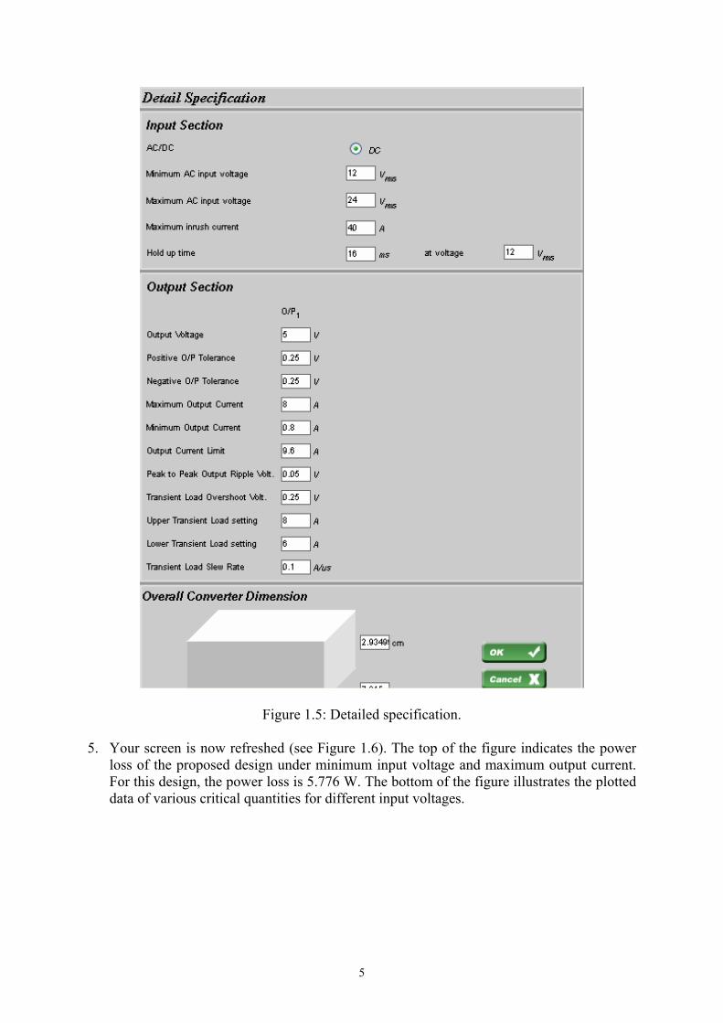
4. Click on Detail Spec. to access the detailed specification of the prescribed converter, i.e.,
tolerance, ripple setting, dynamic requirement, physical dimension etc. Note that you can edit the parameters to change the specification, if necessary. In this exercise, keep the parameters as they are. Click OK to update the settings. The preliminary design for the power supply will be automatically updated.
5
Figure 1.5: Detailed specification.
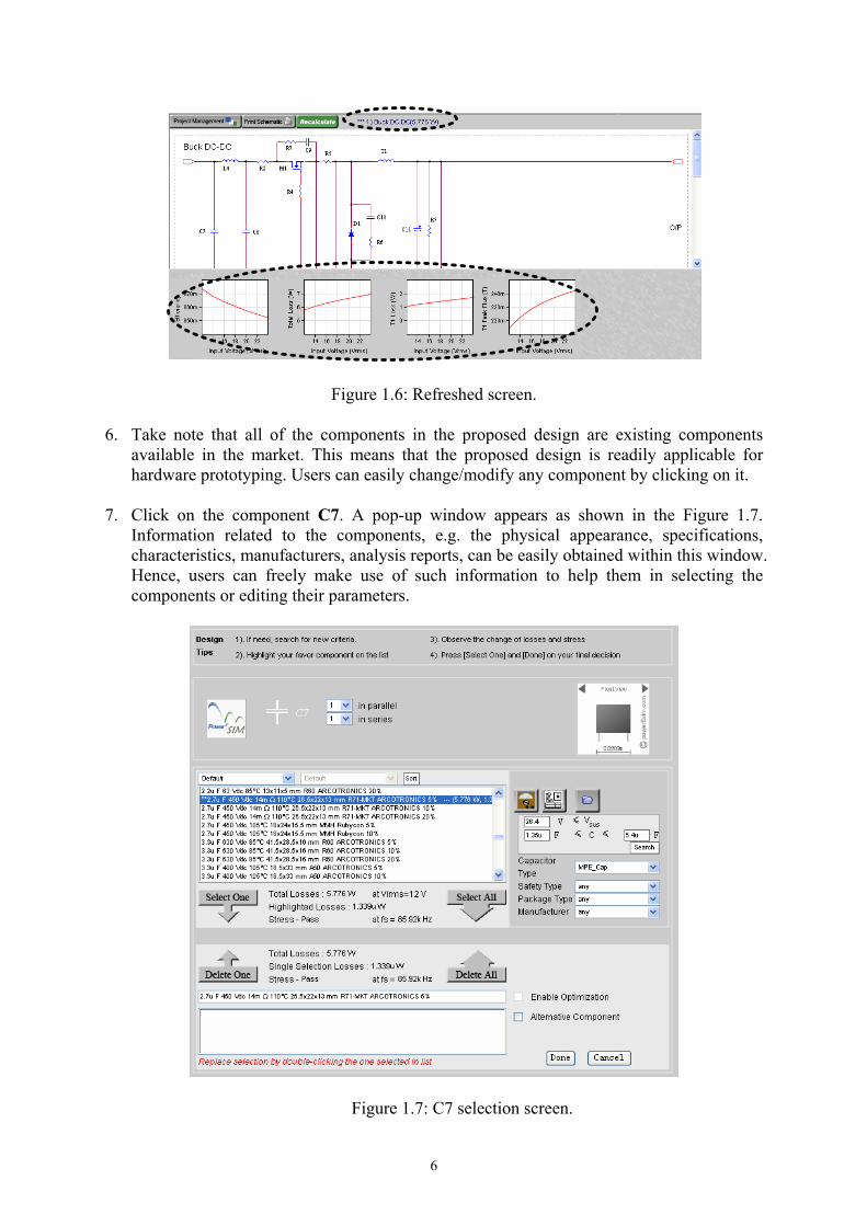
5. Your screen is now refreshed (see Figure 1.6). The top of the figure indicates the power loss of the proposed design under minimum input voltage and maximum output current. For this design, the power loss is 5.776 W. The bottom of the figure illustrates the plotted data of various critical quantities for different input voltages.
6
Figure 1.6: Refreshed screen.
6. Take note that all of the components in the proposed design are existing components available in the market. This means that the proposed design is readily applicable for hardware prototyping. Users can easily change/modify any component by clicking on it.
7. Click on the component C7. A pop-up window appears as shown in the Figure 1.7.
Information related to the components, e.g. the physical appearance, specifications, characteristics, manufacturers, analysis reports, can be easily obtained within this window. Hence, users can freely make use of such information to help them in selecting the components or editing their parameters.
Figure 1.7: C7 selection screen.

7
8. Here, the highlighted component represents the one that is currently considered in the design. One can easily switch to a different component simply by clicking over the key words. Note that for a different component, a different loss and stress will be experienced. This allows users to make their component selections for optimizing the power efficiency and meeting stress requirements.
9. Once the component is chosen, click on Select One and then Done to finalize the change. 10. Remember to click Save or Load to save and load your design at any stage of the
exercises. 11. You have completed Exercise 1 on the basic usage of selection of converter topology and
components. Keeping the existing setup, move on to Exercise 2. 1.5.2 Exercise 2
This exercise aims to introduce the operation and functionality of LosseSIM.
1. Continuing from where you left off in Exercise 1, click on LosseSIM.
Figure 1.8: Loss analysis screen.
8
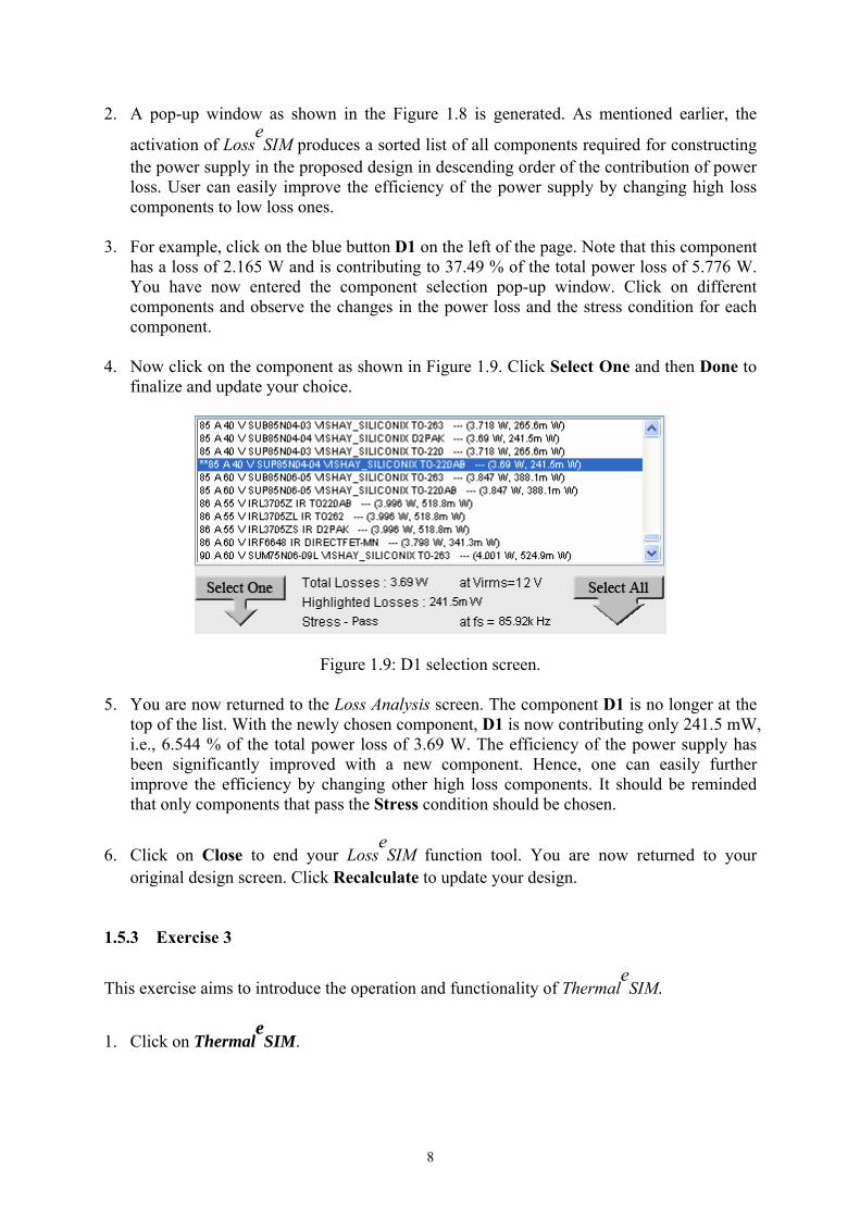
2. A pop-up window as shown in the Figure 1.8 is generated. As mentioned earlier, the
activation of LosseSIM produces a sorted list of all components required for constructing
the power supply in the proposed design in descending order of the contribution of power loss. User can easily improve the efficiency of the power supply by changing high loss components to low loss ones.
3. For example, click on the blue button D1 on the left of the page. Note that this component
has a loss of 2.165 W and is contributing to 37.49 % of the total power loss of 5.776 W. You have now entered the component selection pop-up window. Click on different components and observe the changes in the power loss and the stress condition for each component.
4. Now click on the component as shown in Figure 1.9. Click Select One and then Done to
finalize and update your choice.
Figure 1.9: D1 selection screen.
5. You are now returned to the Loss Analysis screen. The component D1 is no longer at the top of the list. With the newly chosen component, D1 is now contributing only 241.5 mW, i.e., 6.544 % of the total power loss of 3.69 W. The efficiency of the power supply has been significantly improved with a new component. Hence, one can easily further improve the efficiency by changing other high loss components. It should be reminded that only components that pass the Stress condition should be chosen.
6. Click on Close to end your LosseSIM function tool. You are now returned to your
original design screen. Click Recalculate to update your design. 1.5.3 Exercise 3
This exercise aims to introduce the operation and functionality of ThermaleSIM.
1. Click on ThermaleSIM.
9
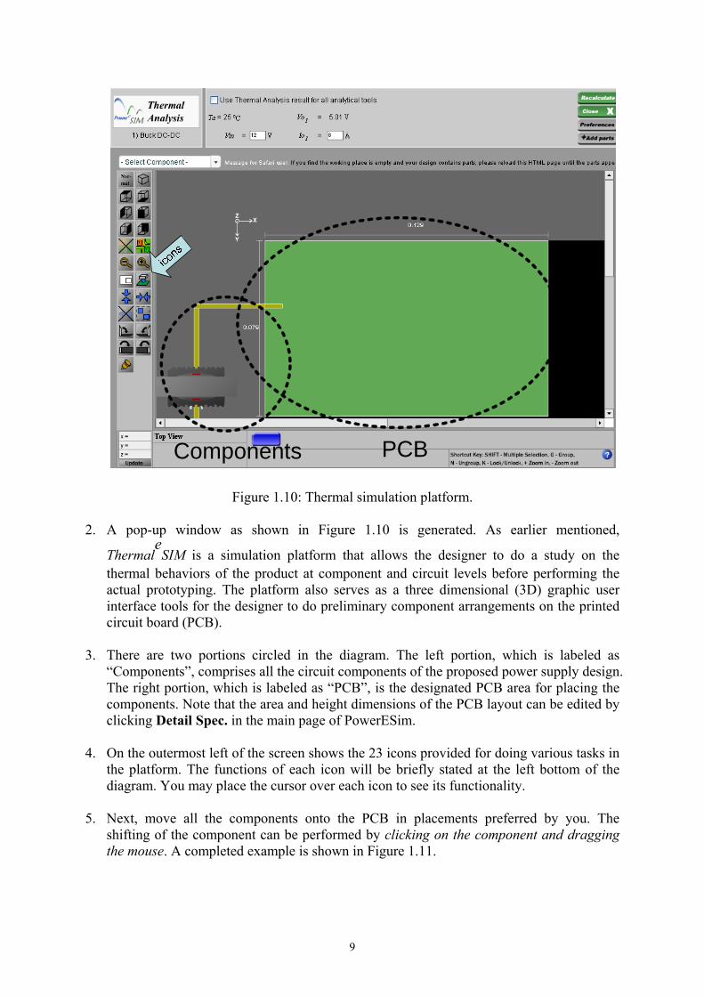
PCBComponents
Figure 1.10: Thermal simulation platform.
2. A pop-up window as shown in Figure 1.10 is generated. As earlier mentioned,
ThermaleSIM is a simulation platform that allows the designer to do a study on the
thermal behaviors of the product at component and circuit levels before performing the actual prototyping. The platform also serves as a three dimensional (3D) graphic user interface tools for the designer to do preliminary component arrangements on the printed circuit board (PCB).
3. There are two portions circled in the diagram. The left portion, which is labeled as
“Components”, comprises all the circuit components of the proposed power supply design. The right portion, which is labeled as “PCB”, is the designated PCB area for placing the components. Note that the area and height dimensions of the PCB layout can be edited by clicking Detail Spec. in the main page of PowerESim.
4. On the outermost left of the screen shows the 23 icons provided for doing various tasks in
the platform. The functions of each icon will be briefly stated at the left bottom of the diagram. You may place the cursor over each icon to see its functionality.
5. Next, move all the components onto the PCB in placements preferred by you. The
shifting of the component can be performed by clicking on the component and dragging the mouse. A completed example is shown in Figure 1.11.
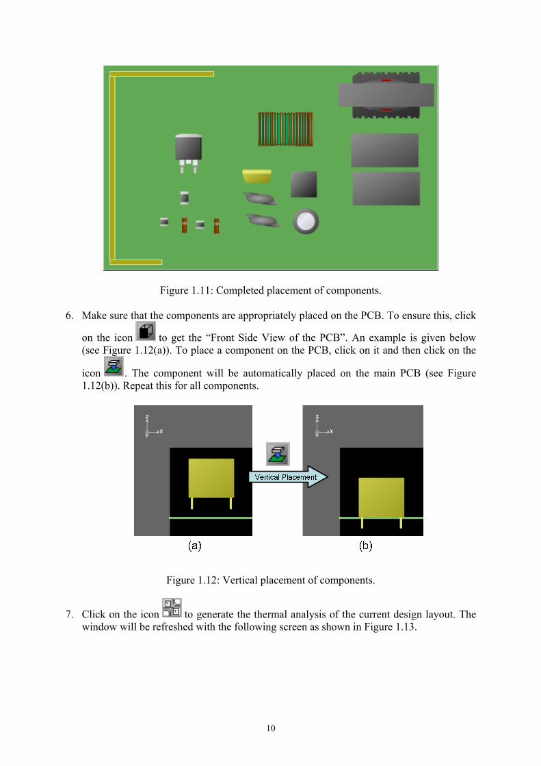
10
Figure 1.11: Completed placement of components.
6. Make sure that the components are appropriately placed on the PCB. To ensure this, click
on the icon to get the “Front Side View of the PCB”. An example is given below (see Figure 1.12(a)). To place a component on the PCB, click on it and then click on the
icon . The component will be automatically placed on the main PCB (see Figure 1.12(b)). Repeat this for all components.
Figure 1.12: Vertical placement of components.
7. Click on the icon to generate the thermal analysis of the current design layout. The window will be refreshed with the following screen as shown in Figure 1.13.

11
Figure 1.13: Thermal analysis layout.
The colour spectrum on the left side of the diagram maps out the component temperature in terms of colour representation. Here, a scale of 19 °C (violet) to 100 °C (pink) is used for easy identification of “hot spot” on the PCB. Pinpoint temperature identification is also provided by the simulation with the actual values stated on the components themselves. For example, the MOSFET M1 in this design and PCB arrangement has an operating temperature of 159 °C.
8. Next, click on the icon to remove the thermal analysis. The thermal analysis must be disabled before you can proceed on to use other function on the platform.
9. Click on the component M1. Click on the icon three times to rotate M1 by 270° in the direction as shown in the Figure 1.14. Now, M1 is placed such that its heat loss surface is parallel to the largest surface area of the heat sink.
Figure 1.14: Rotation of component.
12
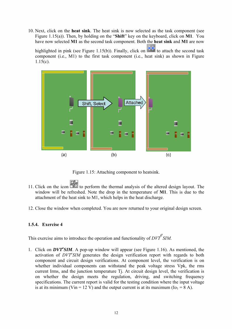
10. Next, click on the heat sink. The heat sink is now selected as the task component (see Figure 1.15(a)). Then, by holding on the “Shift” key on the keyboard, click on M1. You have now selected M1 as the second task component. Both the heat sink and M1 are now
highlighted in pink (see Figure 1.15(b)). Finally, click on to attach the second task component (i.e., M1) to the first task component (i.e., heat sink) as shown in Figure 1.15(c).
Figure 1.15: Attaching component to heatsink.
11. Click on the icon to perform the thermal analysis of the altered design layout. The window will be refreshed. Note the drop in the temperature of M1. This is due to the attachment of the heat sink to M1, which helps in the heat discharge.
12. Close the window when completed. You are now returned to your original design screen. 1.5.4. Exercise 4
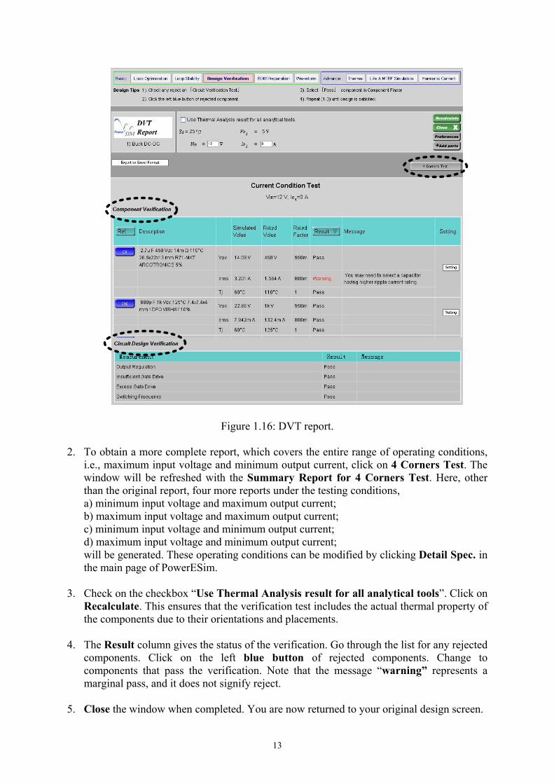
This exercise aims to introduce the operation and functionality of DVTeSIM.
1. Click on DVTeSIM. A pop-up window will appear (see Figure 1.16). As mentioned, the
activation of DVTeSIM generates the design verification report with regards to both component and circuit design verifications. At component level, the verification is on whether individual components can withstand the peak voltage stress Vpk, the rms current Irms, and the junction temperature Tj. At circuit design level, the verification is on whether the design meets the regulation, driving, and switching frequency specifications. The current report is valid for the testing condition where the input voltage is at its minimum (Vin = 12 V) and the output current is at its maximum (Io1 = 8 A).
13
Figure 1.16: DVT report.
2. To obtain a more complete report, which covers the entire range of operating conditions, i.e., maximum input voltage and minimum output current, click on 4 Corners Test. The window will be refreshed with the Summary Report for 4 Corners Test. Here, other than the original report, four more reports under the testing conditions, a) minimum input voltage and maximum output current; b) maximum input voltage and maximum output current; c) minimum input voltage and minimum output current; d) maximum input voltage and minimum output current; will be generated. These operating conditions can be modified by clicking Detail Spec. in the main page of PowerESim.
3. Check on the checkbox “Use Thermal Analysis result for all analytical tools”. Click on Recalculate. This ensures that the verification test includes the actual thermal property of the components due to their orientations and placements.
4. The Result column gives the status of the verification. Go through the list for any rejected
components. Click on the left blue button of rejected components. Change to components that pass the verification. Note that the message “warning” represents a marginal pass, and it does not signify reject.
5. Close the window when completed. You are now returned to your original design screen.
14
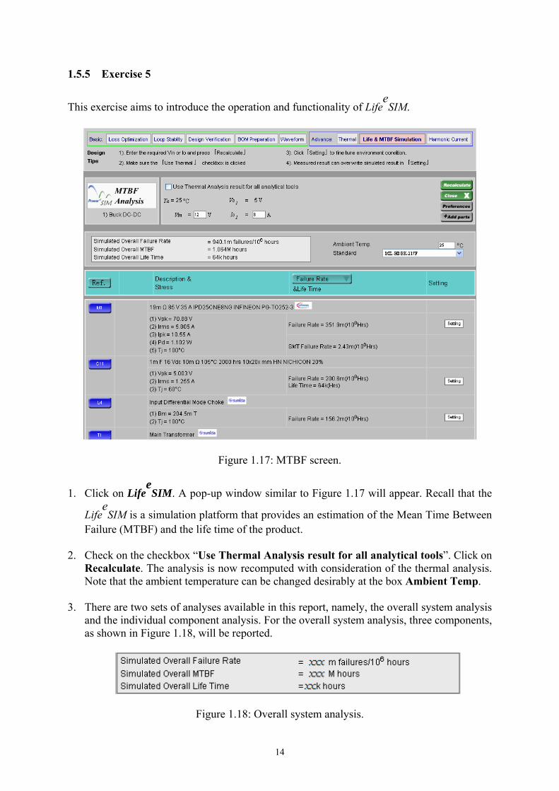
1.5.5 Exercise 5
This exercise aims to introduce the operation and functionality of LifeeSIM.
Figure 1.17: MTBF screen.
1. Click on LifeeSIM. A pop-up window similar to Figure 1.17 will appear. Recall that the
LifeeSIM is a simulation platform that provides an estimation of the Mean Time Between
Failure (MTBF) and the life time of the product. 2. Check on the checkbox “Use Thermal Analysis result for all analytical tools”. Click on
Recalculate. The analysis is now recomputed with consideration of the thermal analysis. Note that the ambient temperature can be changed desirably at the box Ambient Temp.
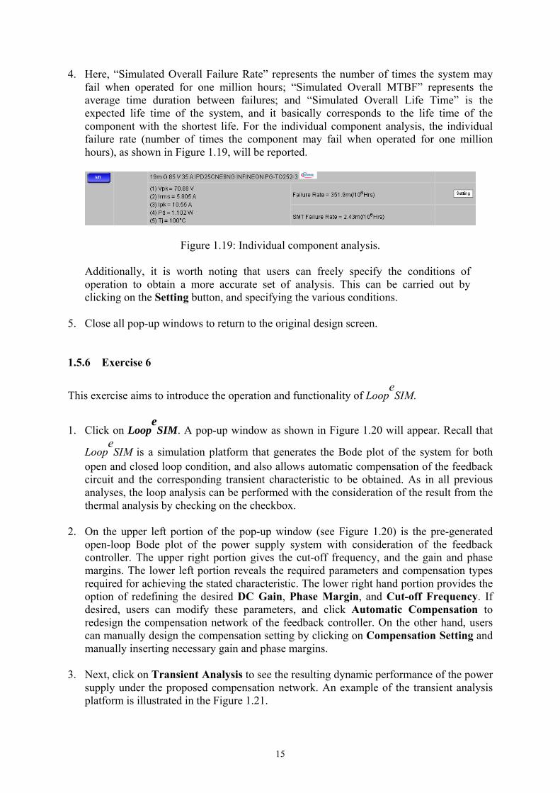
3. There are two sets of analyses available in this report, namely, the overall system analysis
and the individual component analysis. For the overall system analysis, three components, as shown in Figure 1.18, will be reported.
Figure 1.18: Overall system analysis.
15
4. Here, “Simulated Overall Failure Rate” represents the number of times the system may fail when operated for one million hours; “Simulated Overall MTBF” represents the average time duration between failures; and “Simulated Overall Life Time” is the expected life time of the system, and it basically corresponds to the life time of the component with the shortest life. For the individual component analysis, the individual failure rate (number of times the component may fail when operated for one million hours), as shown in Figure 1.19, will be reported.
Figure 1.19: Individual component analysis.
Additionally, it is worth noting that users can freely specify the conditions of operation to obtain a more accurate set of analysis. This can be carried out by clicking on the Setting button, and specifying the various conditions.
5. Close all pop-up windows to return to the original design screen. 1.5.6 Exercise 6
This exercise aims to introduce the operation and functionality of LoopeSIM.
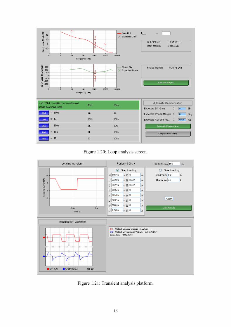
1. Click on LoopeSIM. A pop-up window as shown in Figure 1.20 will appear. Recall that
LoopeSIM is a simulation platform that generates the Bode plot of the system for both
open and closed loop condition, and also allows automatic compensation of the feedback circuit and the corresponding transient characteristic to be obtained. As in all previous analyses, the loop analysis can be performed with the consideration of the result from the thermal analysis by checking on the checkbox.
2. On the upper left portion of the pop-up window (see Figure 1.20) is the pre-generated
open-loop Bode plot of the power supply system with consideration of the feedback controller. The upper right portion gives the cut-off frequency, and the gain and phase margins. The lower left portion reveals the required parameters and compensation types required for achieving the stated characteristic. The lower right hand portion provides the option of redefining the desired DC Gain, Phase Margin, and Cut-off Frequency. If desired, users can modify these parameters, and click Automatic Compensation to redesign the compensation network of the feedback controller. On the other hand, users can manually design the compensation setting by clicking on Compensation Setting and manually inserting necessary gain and phase margins.
3. Next, click on Transient Analysis to see the resulting dynamic performance of the power
supply under the proposed compensation network. An example of the transient analysis platform is illustrated in the Figure 1.21.
16
Figure 1.20: Loop analysis screen.
Figure 1.21: Transient analysis platform.
17
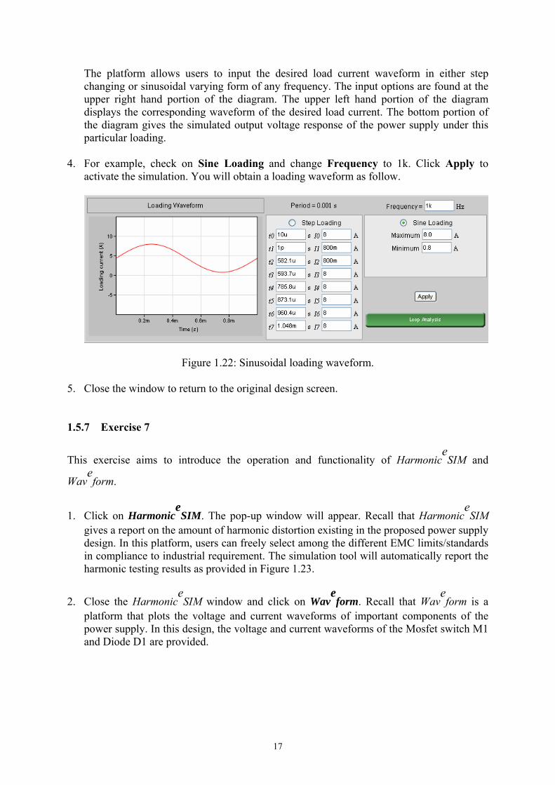
The platform allows users to input the desired load current waveform in either step changing or sinusoidal varying form of any frequency. The input options are found at the upper right hand portion of the diagram. The upper left hand portion of the diagram displays the corresponding waveform of the desired load current. The bottom portion of the diagram gives the simulated output voltage response of the power supply under this particular loading.
4. For example, check on Sine Loading and change Frequency to 1k. Click Apply to activate the simulation. You will obtain a loading waveform as follow.
Figure 1.22: Sinusoidal loading waveform.
5. Close the window to return to the original design screen. 1.5.7 Exercise 7
This exercise aims to introduce the operation and functionality of HarmoniceSIM and
Waveform.
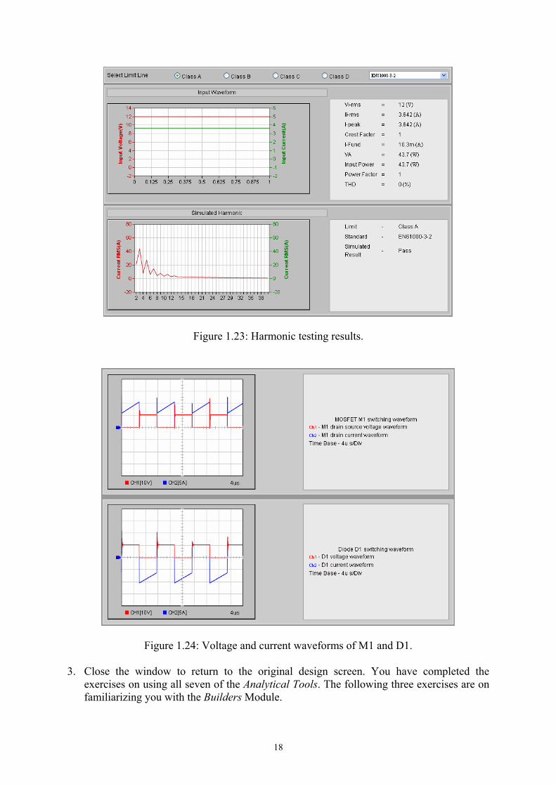
1. Click on HarmoniceSIM. The pop-up window will appear. Recall that Harmonic
eSIM
gives a report on the amount of harmonic distortion existing in the proposed power supply design. In this platform, users can freely select among the different EMC limits/standards in compliance to industrial requirement. The simulation tool will automatically report the harmonic testing results as provided in Figure 1.23.
2. Close the HarmoniceSIM window and click on Wav
eform. Recall that Wav
eform is a
platform that plots the voltage and current waveforms of important components of the power supply. In this design, the voltage and current waveforms of the Mosfet switch M1 and Diode D1 are provided.
18
Figure 1.23: Harmonic testing results.
Figure 1.24: Voltage and current waveforms of M1 and D1.
3. Close the window to return to the original design screen. You have completed the exercises on using all seven of the Analytical Tools. The following three exercises are on familiarizing you with the Builders Module.

19
1.5.8 Exercise 8 This exercise aims to introduce the operation and functionality of Magnetic Builder. Recall that Magnetic Builder is a design platform for users to create their own magnetic components by selecting different ferrite cores, bobbin (container) types, and the winding methods. 1. Click on Magnetic Builder. A pop-up window appears as shown in Figure 1.25. Change
“Number of Secondary Windings” to 0 and click OK.
Figure 1.25: Magnetic builder popup screen.
Figure 1.26: Magnetic builder selection screen.
2. The window will be refreshed as shown in Figure 1.26. Click on and try changing
the inductance to 50 μH. Next, note that clicking on the icon will introduce a
20
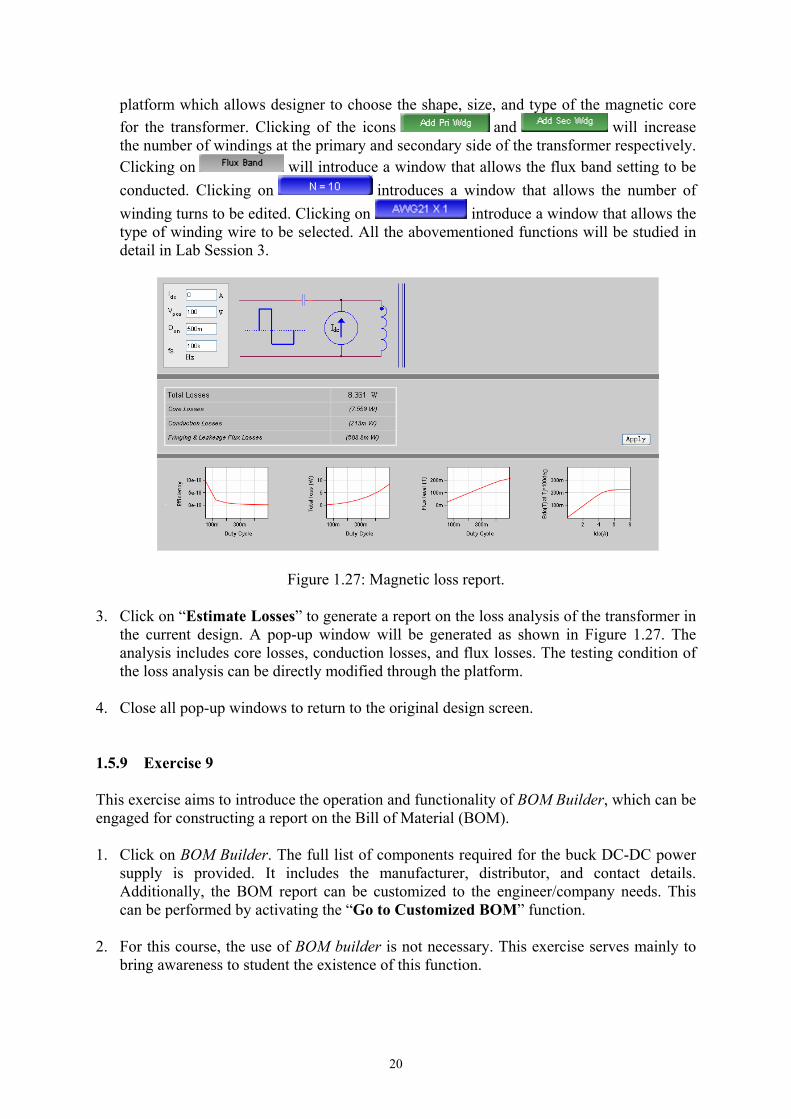
platform which allows designer to choose the shape, size, and type of the magnetic core for the transformer. Clicking of the icons and will increase the number of windings at the primary and secondary side of the transformer respectively. Clicking on will introduce a window that allows the flux band setting to be conducted. Clicking on introduces a window that allows the number of winding turns to be edited. Clicking on introduce a window that allows the type of winding wire to be selected. All the abovementioned functions will be studied in detail in Lab Session 3.
Figure 1.27: Magnetic loss report.
3. Click on “Estimate Losses” to generate a report on the loss analysis of the transformer in the current design. A pop-up window will be generated as shown in Figure 1.27. The analysis includes core losses, conduction losses, and flux losses. The testing condition of the loss analysis can be directly modified through the platform.
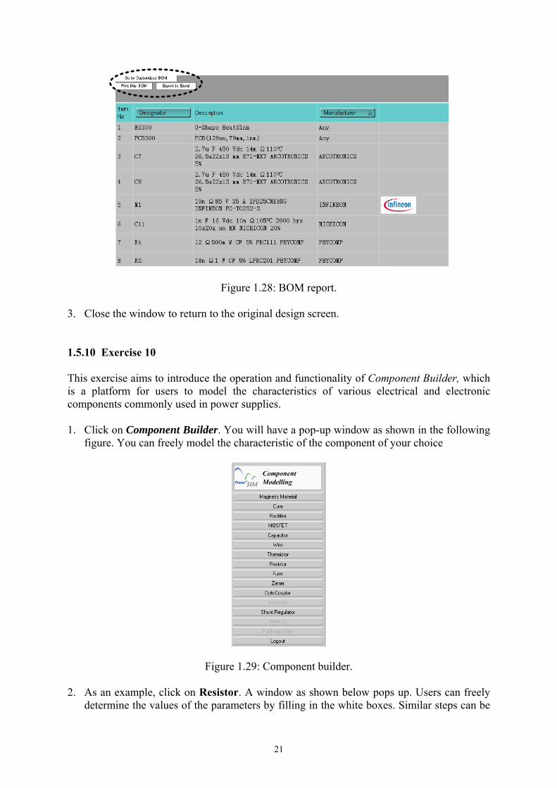
4. Close all pop-up windows to return to the original design screen. 1.5.9 Exercise 9 This exercise aims to introduce the operation and functionality of BOM Builder, which can be engaged for constructing a report on the Bill of Material (BOM). 1. Click on BOM Builder. The full list of components required for the buck DC-DC power
supply is provided. It includes the manufacturer, distributor, and contact details. Additionally, the BOM report can be customized to the engineer/company needs. This can be performed by activating the “Go to Customized BOM” function.
2. For this course, the use of BOM builder is not necessary. This exercise serves mainly to
bring awareness to student the existence of this function.
21
Figure 1.28: BOM report.
3. Close the window to return to the original design screen. 1.5.10 Exercise 10 This exercise aims to introduce the operation and functionality of Component Builder, which is a platform for users to model the characteristics of various electrical and electronic components commonly used in power supplies. 1. Click on Component Builder. You will have a pop-up window as shown in the following
figure. You can freely model the characteristic of the component of your choice
Figure 1.29: Component builder.
2. As an example, click on Resistor. A window as shown below pops up. Users can freely determine the values of the parameters by filling in the white boxes. Similar steps can be

22
taken to characterize other components in Component Builder.
Figure 1.30: Resistor builder screen.
3. Close all pop-up windows to return to the original design screen. 1.6 Assignment Having completed all the exercises, it is now time to practice what you have learnt in this laboratory. As a home assignment, do the following. 1. Generate a preliminary design of a Boost DC-DC power supply that operates with
maximum and minimum input voltages of 12 V and 8 V, an output voltage of 24 V, and a maximum output current of 2 A. (Hint: Refer to Exercise 1.)
2. Optimize the power efficiency of your design by using different components. You should
reduce the total power loss to less than 6 W. (Hint: Refer to Exercise 2.) 3. Generate the 4 Corners Test report for the design. (Hint: Refer to Exercise 4.) 4. Generate the MTBF Analysis report for the design. (Hint: Refer to Exercise 5.) 5. Generate Bode plot of the system and the compensation requirement. Show also the result
of the transient analysis. (Hint: Refer to Exercise 6.) 6. Generate the critical voltage and current waveforms of the design. (Hint: Refer to
Exercise 7.) Finally, submit a complete report evaluating the different aspects of your power supply design. Attach all reports, analyses, and waveforms generated that are relevant to the discussion.
23
Laboratory 2
Understanding the Characteristics of Buck and Boost Converters and Their Control
2.1 Objectives 1. To study the transient and steady-state properties of the buck and boost converters with
respect to circuit parameters using the PowerESim package. 2. To understand the two common control methods, namely, voltage mode control and
current mode control, and their feedback circuits as applied to the buck and boost converters using the PowerESim package.
2.2 Introduction
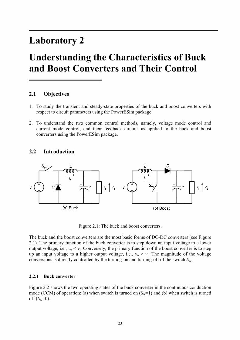
Figure 2.1: The buck and boost converters.
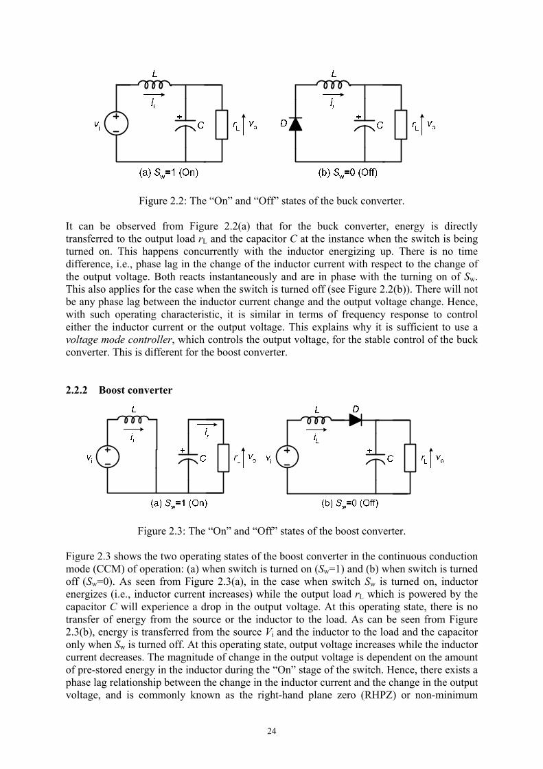
The buck and the boost converters are the most basic forms of DC-DC converters (see Figure 2.1). The primary function of the buck converter is to step down an input voltage to a lower output voltage, i.e., vo < vi. Conversely, the primary function of the boost converter is to step up an input voltage to a higher output voltage, i.e., vo > vi. The magnitude of the voltage conversions is directly controlled by the turning-on and turning-off of the switch Sw. 2.2.1 Buck converter Figure 2.2 shows the two operating states of the buck converter in the continuous conduction mode (CCM) of operation: (a) when switch is turned on (Sw=1) and (b) when switch is turned off (Sw=0).
24
Figure 2.2: The “On” and “Off” states of the buck converter.
It can be observed from Figure 2.2(a) that for the buck converter, energy is directly transferred to the output load rL and the capacitor C at the instance when the switch is being turned on. This happens concurrently with the inductor energizing up. There is no time difference, i.e., phase lag in the change of the inductor current with respect to the change of the output voltage. Both reacts instantaneously and are in phase with the turning on of Sw. This also applies for the case when the switch is turned off (see Figure 2.2(b)). There will not be any phase lag between the inductor current change and the output voltage change. Hence, with such operating characteristic, it is similar in terms of frequency response to control either the inductor current or the output voltage. This explains why it is sufficient to use a voltage mode controller, which controls the output voltage, for the stable control of the buck converter. This is different for the boost converter. 2.2.2 Boost converter
Figure 2.3: The “On” and “Off” states of the boost converter.
Figure 2.3 shows the two operating states of the boost converter in the continuous conduction mode (CCM) of operation: (a) when switch is turned on (Sw=1) and (b) when switch is turned off (Sw=0). As seen from Figure 2.3(a), in the case when switch Sw is turned on, inductor energizes (i.e., inductor current increases) while the output load rL which is powered by the capacitor C will experience a drop in the output voltage. At this operating state, there is no transfer of energy from the source or the inductor to the load. As can be seen from Figure 2.3(b), energy is transferred from the source Vi and the inductor to the load and the capacitor only when Sw is turned off. At this operating state, output voltage increases while the inductor current decreases. The magnitude of change in the output voltage is dependent on the amount of pre-stored energy in the inductor during the “On” stage of the switch. Hence, there exists a phase lag relationship between the change in the inductor current and the change in the output voltage, and is commonly known as the right-hand plane zero (RHPZ) or non-minimum

25
phase response property. Therefore, unlike the buck converter, the control of the inductor current or the output voltage state variable in the boost converter does not offer the same frequency performance in terms of converter regulation. Even though it is possible to use a voltage mode controller with the boost converter, it can only be realized at a reduced frequency bandwidth. For a higher bandwidth (faster) response, a current mode controller, which controls the inductor current, is required for the stable control of the boost converter. Additionally, for a better understanding of the buck and boost converters operation in the discontinuous conduction mode of operation, please refer to [1], [2]. 2.2.3 Controller The two most commonly used control techniques in DC-DC power supplies are the fixed-frequency pulse-width-modulation (PWM) voltage mode control and peak current mode control. The voltage mode control is a single-loop control where the output voltage is regulated by closing a feedback loop between the output voltage and the duty-ratio signal (see Figure 2.4(a)). The output voltage is compared with a constant reference signal Vref to give the error, which is then passed through the compensation network Zf to generate a control signal. The PWM modulator then compares this compensated control signal with the externally generated ramp signal vramp to generate the desired control signal for driving the power switch.
+vi
+vo
-
L
D C rL
SW
VREF
_
+vramp
R1
R2
+_
Zf
PWM
Figure 2.4: Overview of voltage mode control and peak current mode control.
On the other hand, the peak current mode control is a two-loop control system which uses an inner current loop (i.e., inductor current or power switch current) in addition to the voltage feedback loop (see Figure 2.4(b)). The aim of this control is to force the peak inductor current to follow a reference signal which is derived from the output voltage feedback loop. The idea is to turn on the power switch SW at periodic cycles commanded by a fixed-frequency clock signal, and to turn it off when the peak of the instantaneous current touches the desired reference level. According to [3], [4], the advantages and disadvantages of using peak current mode control over voltage mode control can be summarized as follows.

26
Advantages: 1. Easier to perform control compensation with current mode control than voltage mode
control, especially with the presence of right-half plane zero; 2. Current mode control has inherent input current limiting and line rejection capability. For
voltage mode control, external over-current protection and input feedforward circuitries are required.
Disadvantages: 1. Current mode control requires an additional current sensor as compared to voltage mode
control; 2. Peak current mode control can be unstable when the duty cycle of the converter
approaches 50%. This is known as sub-harmonic oscillation. Typically, a compensating ramp (with slope equal to the inductor current downslope) is required at the comparator input to eliminate this instability;
3. Current mode control has a high Signal-to-Noise Ratio and the control is more easily
affected by noise signal than voltage mode control. Apart from selecting the proper controller, it is also the power supply designer’s duty to choose suitable compensation network Zf to achieve the desired regulation and dynamic performances in the converters. For information concerning the average current mode control, please refer to [5]. 2.2.4 Storage Elements It is known that the size of the inductive and capacitive energy storage tanks, i.e., L and C affects the dynamic performance of the DC-DC converter. This can be understood by examining the operating mechanism of these elements. Since the rate of storing/releasing electrical energy, i.e., τ = rLC (capacitor) and τ = L/rL (inductor), is directly affected by the value of the energy storage elements, the ability to respond to the load changes is therefore also affected by the size of the energy storages. Specifically, for a fixed-frequency operation, the dynamic response of the regulation will be faster with smaller values of L or C, since smaller energy storage elements require a shorter time to store and release energy. On the other hand, a smaller value of L will lead to a higher-ripple inductor current and a smaller output voltage undershoot or overshoot during a step increment or step decrement in the load current. Yet, a larger value of C will give a smaller output voltage undershoot during a step increment in the load current, and a smaller output voltage overshoot during a step decrement in the load current. All these aspects shape the dynamic behavior of the converter.

27
2.3 Exercises 2.3.1 Exercise 1 This exercise aims to inform student the typical open-loop characteristic of the buck DC-DC converters and how different converter parameters affect this characteristic. 1. Log in to PowerESim. 2. Click on . Save both the Lecture 2 Buck Converter Template and Lecture 2
Boost Converter Template from the tutorial section of the pop-up window onto the “Desktop” of the computer. Close the pop-up window.
3. Load the buck converter model into the simulation platform.
Procedure: a) Click on . b) In the Load Project window, click on Browse. Select the path “Desktop” and double
click on Buck_PolyU.pesim.
c) Click on Load Design.
d) The proposed buck converter design has the following specification: VinMax = 24 Vrms, VinMin = 12 Vrms, Vo1 = 5 V, and Io1 = 8 A.
4. Scroll down to the bottom of the schematic diagram, which displays the default generic
feedback controller of the converter, as shown in Figure 2.5.
Figure 2.5: Schematic of feedback controller in proposed buck DC-DC converter.
The right side of the figure shows the “Non-Isolated Generic Feedback Block”. This is basically a general error amplifier circuit for controlling the output voltage variable Vo. Vref signifies the reference tracking voltage and the combination of resistors Rb1 to Rb5 and capacitors Cb1 to Cb3 forms the general compensation network of the error amplifier.
28
With different combinative parameters for these resistive and capacitive components, a whole range of compensation is possible. The output of the amplifier is fed into the positive pin of PWM comparator on the left side of the figure, which is labeled as “Generic I-mode High Side Drive PWM Block”, via buffer (x1), voltage divider network (Rpwm4 and Rpwm5), and voltage clamp Vcs. The negative pin of the PWM comparator is tied to a gain amplifier Gcs, with input corresponding to the summation of the slope compensation (ramp signal) and the filtered inductor current. Note that the sensing of the inductor current is carried out by the resistor R5 in the power circuit and the inductor current filter is constructed through Rpwm6, Rpwm7, and Cpwm3. The output of the PWM comparator gives the discrete switching pulse and is fed to the Reset pin of the RS flip flop. The Set pin of the flip flop is tied to a square wave oscillator.
5. To obtain the open-loop converter characteristic, the compensation of the controller must be modified to achieve a high DC gain and flat ac gain of 1 at frequency higher than 0.2 Hz. This can be achieved by changing the component parameters to the values given in the following table.
Cfb1 = 0.1 pF Rfb5 = 20 MΩ Rfb6 = 41 kΩ
Rfb2 = 20 MΩ Cfb2 = 0.1 pF Cfb3 = 100 μF
Rpwm6 = 10 MΩ Rpwm7 = 1 Ω Vpeak = 333 mV
Table 2.1: Parameters of controller for achieving open-loop buck converter.
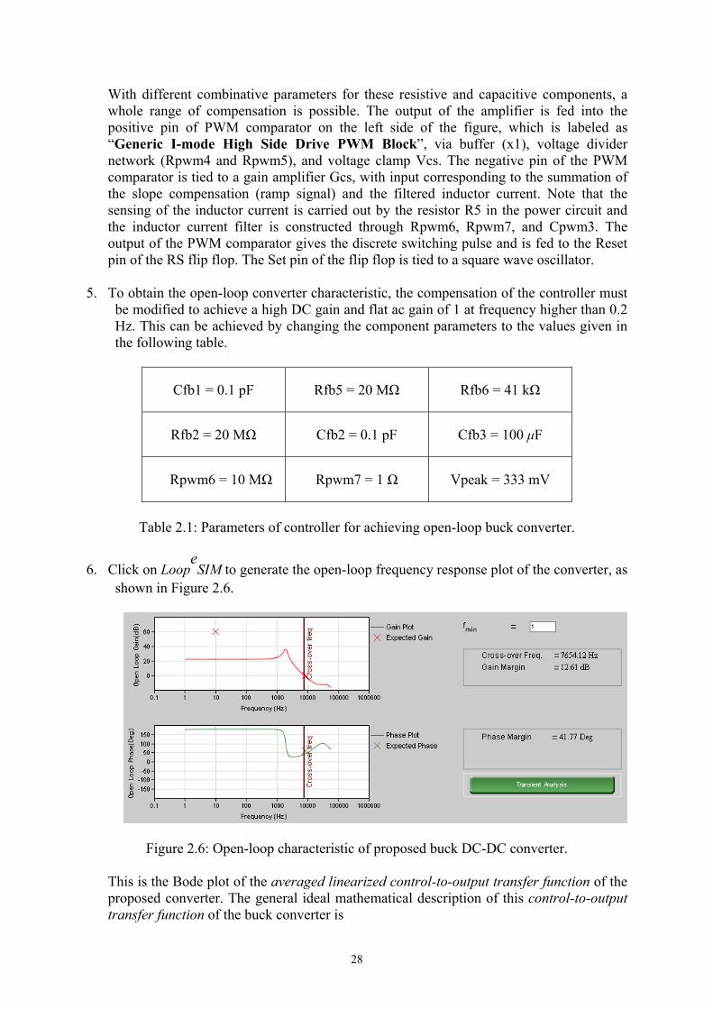
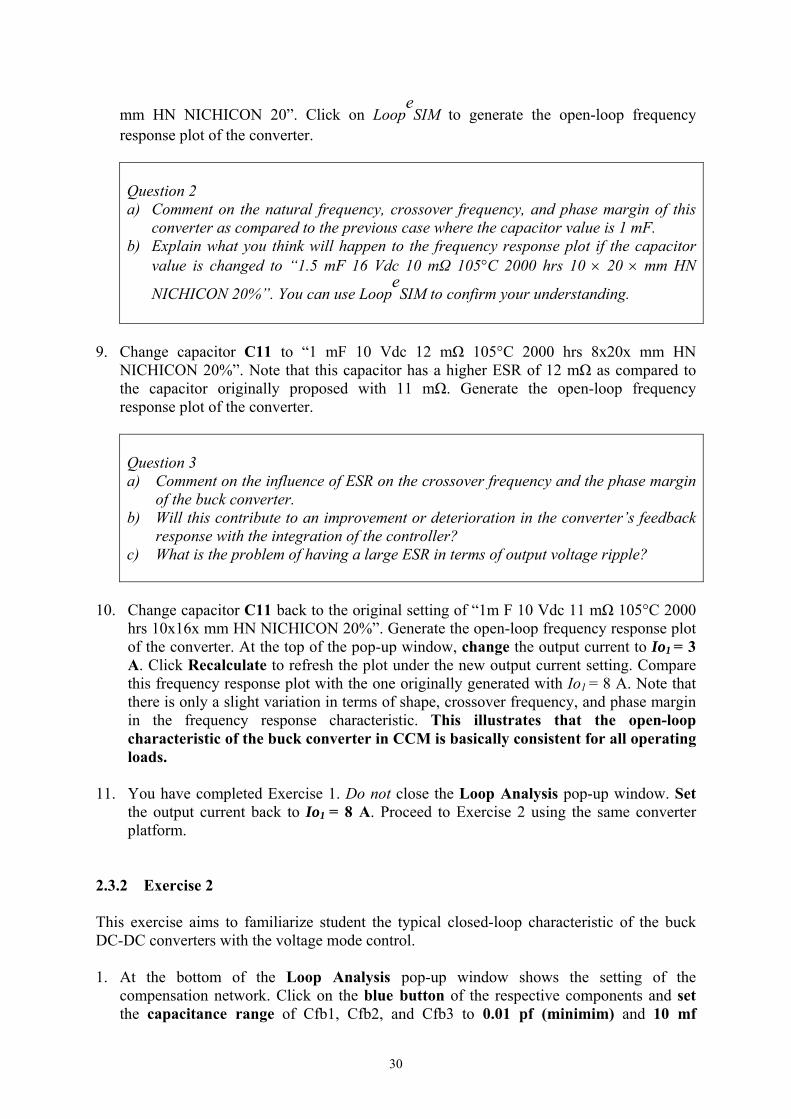
6. Click on LoopeSIM to generate the open-loop frequency response plot of the converter, as
shown in Figure 2.6.
Figure 2.6: Open-loop characteristic of proposed buck DC-DC converter.
This is the Bode plot of the averaged linearized control-to-output transfer function of the proposed converter. The general ideal mathematical description of this control-to-output transfer function of the buck converter is
29
.1
1)(~)(~
)(2LCssCR
rL
CsRVsdsvsG
ESRL
ESRi
ovd
+⎟⎟⎠
⎞⎜⎜⎝
⎛++
+≈=
From the equation above, it can be noticed that the open-loop small-signal description of
the buck converter has a double pole at LC
fP π21
= and a zero at CR
fESR
Z π21
= .
Typically, for the buck converter, this double pole occurs before the crossover frequency and the zero which is influenced by the capacitor’s equivalent series resistance RESR occurs after the crossover frequency. Hence, the effective description of the buck converter below the crossover frequency is dominantly an input voltage passing through a lowpass filter. This can be reflected from the gain-phase plot. Note that with the input voltage Vi = 12 V, the dB gain (dB) is around 20 log Vi = 21.6 dB for frequency up to 800 Hz (see Open Loop Gain (dB) plot). Additionally, it is also shown that a resonance (peaking) response which causes a sudden increment in dB gain occurs at 1927 Hz. This corresponds the natural frequency of the converter’s LC tank, which is
Hz1927mF1H82.62
1=
×=
μπPf . Following the resonance response, the dB gain drops
at 40 dB per decade. The zero occurs at Hz6.14468mF1m112
1=
×Ω×=
πZf . From the
simulation, it is given that for the proposed converter, the open-loop crossover frequency is 7654.12 Hz and the phase margin is 41.77 degree. It is known that with the integration of the feedback controller, systems with a higher crossover frequency gives a faster dynamic response as compared to system with a lower crossover frequency. Furthermore, in practical power supplies, a closed-loop phase margin of at least 45 to 60 degree is typically required for the stability of the regulation.
7. Next, close the pop-up window and return to the main page of PowerESim. Change the
value of the inductor T1 of the buck converter to 15 μH. Click on LoopeSIM to generate
the open-loop frequency response plot of the converter.
Question 1 a) Comment on the natural frequency, crossover frequency, and phase margin of this
converter as compared to the previous case where the inductor value is 6.82 μH. b) Explain what you think will happen to the frequency response plot if the inductor
value is changed to 3 μH. You can use LoopeSIM to confirm your understanding.
Will this contribute to an improvement or deterioration in the converter’s feedback response with the integration of the controller?
c) What could be the problem in terms of converter’s operation when the inductance is too small?
8. Close the pop-up window and reset the value of the inductor T1 to 6.82 μH. The present
capacitor C11 in the converter is “1m F 10 Vdc 11 mΩ 105°C 2000 hrs 10x16x mm HN NICHICON 20%”. Change C11 to “820 uF 16 Vdc 11 mΩ 105°C 2000 hrs 10 × 16 ×
30
mm HN NICHICON 20”. Click on LoopeSIM to generate the open-loop frequency
response plot of the converter.
Question 2 a) Comment on the natural frequency, crossover frequency, and phase margin of this
converter as compared to the previous case where the capacitor value is 1 mF. b) Explain what you think will happen to the frequency response plot if the capacitor
value is changed to “1.5 mF 16 Vdc 10 mΩ 105°C 2000 hrs 10 × 20 × mm HN
NICHICON 20%”. You can use LoopeSIM to confirm your understanding.
9. Change capacitor C11 to “1 mF 10 Vdc 12 mΩ 105°C 2000 hrs 8x20x mm HN
NICHICON 20%”. Note that this capacitor has a higher ESR of 12 mΩ as compared to the capacitor originally proposed with 11 mΩ. Generate the open-loop frequency response plot of the converter.
Question 3 a) Comment on the influence of ESR on the crossover frequency and the phase margin
of the buck converter. b) Will this contribute to an improvement or deterioration in the converter’s feedback
response with the integration of the controller? c) What is the problem of having a large ESR in terms of output voltage ripple?
10. Change capacitor C11 back to the original setting of “1m F 10 Vdc 11 mΩ 105°C 2000
hrs 10x16x mm HN NICHICON 20%”. Generate the open-loop frequency response plot of the converter. At the top of the pop-up window, change the output current to Io1 = 3 A. Click Recalculate to refresh the plot under the new output current setting. Compare this frequency response plot with the one originally generated with Io1 = 8 A. Note that there is only a slight variation in terms of shape, crossover frequency, and phase margin in the frequency response characteristic. This illustrates that the open-loop characteristic of the buck converter in CCM is basically consistent for all operating loads.
11. You have completed Exercise 1. Do not close the Loop Analysis pop-up window. Set
the output current back to Io1 = 8 A. Proceed to Exercise 2 using the same converter platform.
2.3.2 Exercise 2 This exercise aims to familiarize student the typical closed-loop characteristic of the buck DC-DC converters with the voltage mode control. 1. At the bottom of the Loop Analysis pop-up window shows the setting of the
compensation network. Click on the blue button of the respective components and set the capacitance range of Cfb1, Cfb2, and Cfb3 to 0.01 pf (minimim) and 10 mf
31
(maximum), and resistance range of Rfb2 and Rfb6 to 1 Ω (minimum) and 20 MΩ (maximum). For example, the range setting of Cfb1 can be performed by writing over the white boxes in with the desired parameter. Click Done to update. Repeat for all other components. The setting allows the computer simulation to search for the optimal compensation network within the preset ranges of capacitance and resistance values (see Figure 2.7).
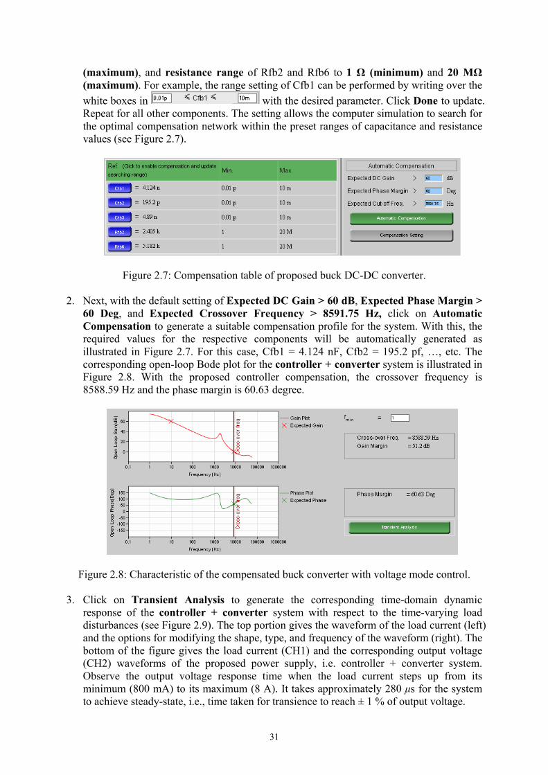
Figure 2.7: Compensation table of proposed buck DC-DC converter.
2. Next, with the default setting of Expected DC Gain > 60 dB, Expected Phase Margin > 60 Deg, and Expected Crossover Frequency > 8591.75 Hz, click on Automatic Compensation to generate a suitable compensation profile for the system. With this, the required values for the respective components will be automatically generated as illustrated in Figure 2.7. For this case, Cfb1 = 4.124 nF, Cfb2 = 195.2 pf, …, etc. The corresponding open-loop Bode plot for the controller + converter system is illustrated in Figure 2.8. With the proposed controller compensation, the crossover frequency is 8588.59 Hz and the phase margin is 60.63 degree.
Figure 2.8: Characteristic of the compensated buck converter with voltage mode control.
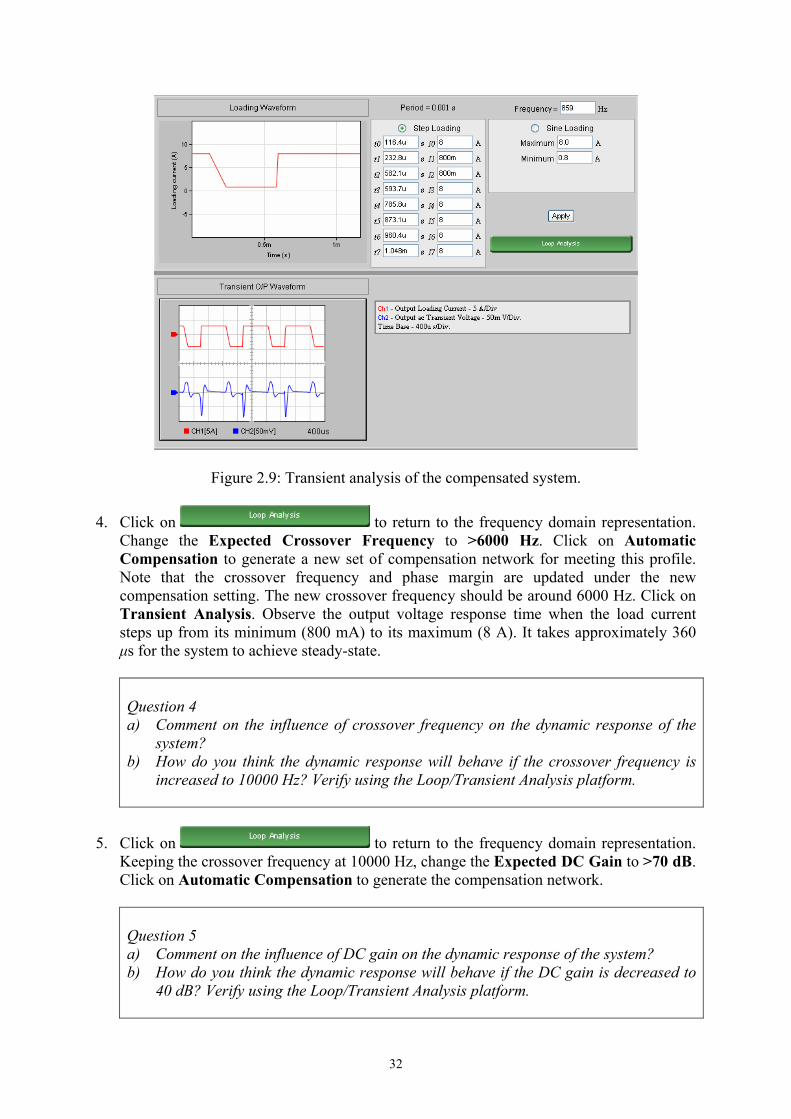
3. Click on Transient Analysis to generate the corresponding time-domain dynamic response of the controller + converter system with respect to the time-varying load disturbances (see Figure 2.9). The top portion gives the waveform of the load current (left) and the options for modifying the shape, type, and frequency of the waveform (right). The bottom of the figure gives the load current (CH1) and the corresponding output voltage (CH2) waveforms of the proposed power supply, i.e. controller + converter system. Observe the output voltage response time when the load current steps up from its minimum (800 mA) to its maximum (8 A). It takes approximately 280 μs for the system to achieve steady-state, i.e., time taken for transience to reach ± 1 % of output voltage.
32
Figure 2.9: Transient analysis of the compensated system.
4. Click on to return to the frequency domain representation. Change the Expected Crossover Frequency to >6000 Hz. Click on Automatic Compensation to generate a new set of compensation network for meeting this profile. Note that the crossover frequency and phase margin are updated under the new compensation setting. The new crossover frequency should be around 6000 Hz. Click on Transient Analysis. Observe the output voltage response time when the load current steps up from its minimum (800 mA) to its maximum (8 A). It takes approximately 360 μs for the system to achieve steady-state.
Question 4 a) Comment on the influence of crossover frequency on the dynamic response of the
system? b) How do you think the dynamic response will behave if the crossover frequency is
increased to 10000 Hz? Verify using the Loop/Transient Analysis platform.
5. Click on to return to the frequency domain representation.
Keeping the crossover frequency at 10000 Hz, change the Expected DC Gain to >70 dB. Click on Automatic Compensation to generate the compensation network.
Question 5 a) Comment on the influence of DC gain on the dynamic response of the system? b) How do you think the dynamic response will behave if the DC gain is decreased to
40 dB? Verify using the Loop/Transient Analysis platform.
33
6. Next, set the Expected DC Gain to >80 dB and Expected Crossover Frequency to >20000 Hz and generate the corresponding compensation network. Observe the transient response of the output voltage for the load disturbance. Note the significant improvement in the dynamic response, i.e. shorter settling time and smaller overshoot ripple.
7. Now, increase the Expected Crossover Frequency to >21000 Hz and generate the
corresponding compensation network. Observe the transient response of the output voltage for the load disturbance. You will see that the output voltage response is oscillatory. This is known as output voltage regulation instability. Note that in this case, the instability is not due to the –ve phase margin. Instead, it is due to the crossover frequency being too high for this system. To prevent this kind instability, it is a typical practice in buck converter design to set the crossover frequency below ¼ of the switching frequency. The current setting of the switching frequency is 85.92 kHz. Change the switching frequency to 114.5 kHz. You can do this by going to the main page of PowerESim and click on the wording “fosc” of the clock generator at the bottom of the controller (see Figure 2.10). Select 114.5 kHz and click Done.
Figure 2.10: Clock generator symbol.
Go back to the Loop Analysis platform and generate the compensation network for the new frequency. Switch to Transient Analysis and observe the output voltage waveform. The output voltage regulation is now stable. Question 6 Why do you think this happens?
8. Set the switching frequency of the clock generator back to 85.91 kHz. Next, set the
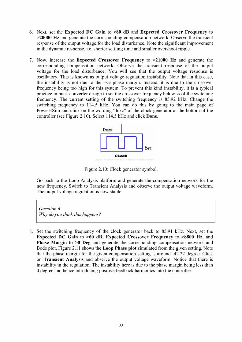
Expected DC Gain to >60 dB, Expected Crossover Frequency to >8800 Hz, and Phase Margin to >0 Deg and generate the corresponding compensation network and Bode plot. Figure 2.11 shows the Loop Phase plot simulated from the given setting. Note that the phase margin for the given compensation setting is around -42.22 degree. Click on Transient Analysis and observe the output voltage waveform. Notice that there is instability in the regulation. The instability here is due to the phase margin being less than 0 degree and hence introducing positive feedback harmonics into the controller.
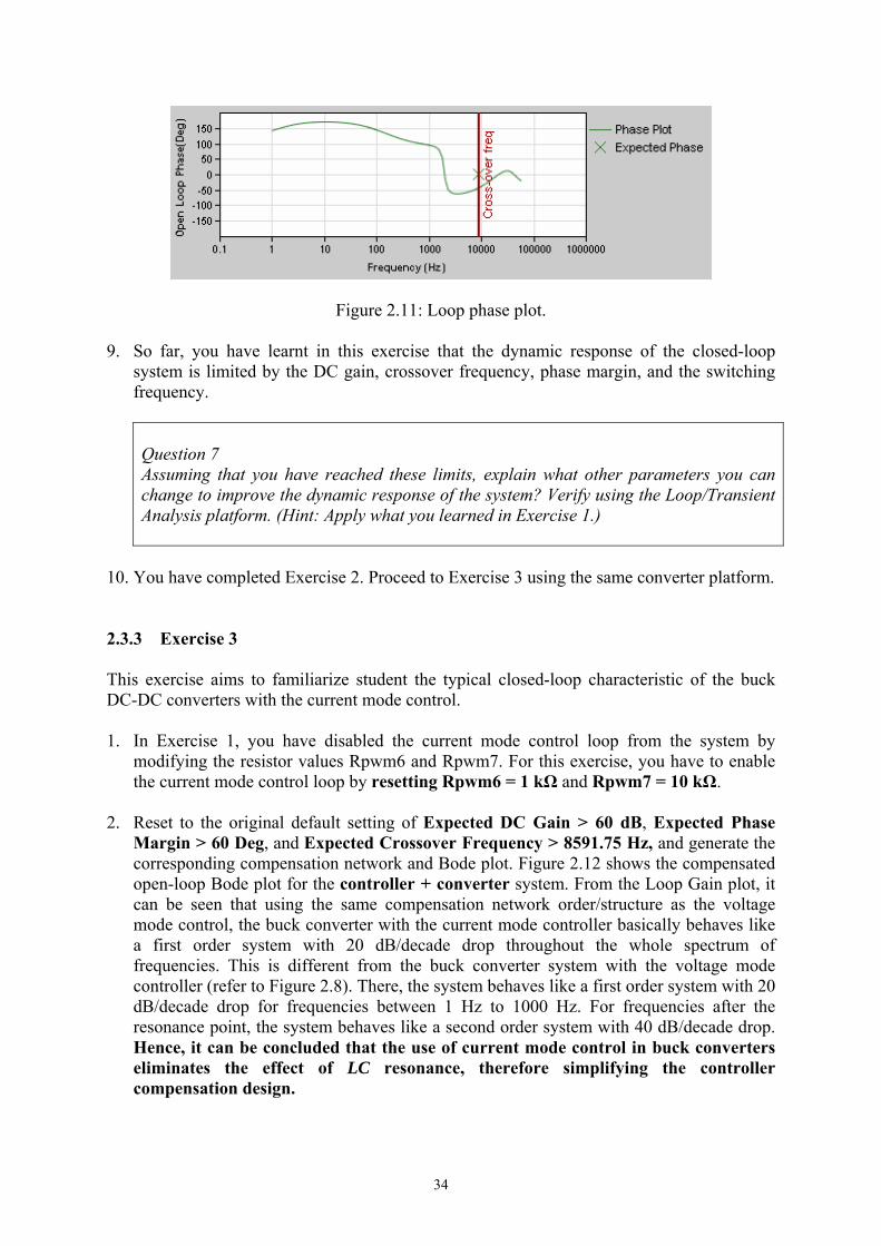
34
Figure 2.11: Loop phase plot.
9. So far, you have learnt in this exercise that the dynamic response of the closed-loop system is limited by the DC gain, crossover frequency, phase margin, and the switching frequency.
Question 7 Assuming that you have reached these limits, explain what other parameters you can change to improve the dynamic response of the system? Verify using the Loop/Transient Analysis platform. (Hint: Apply what you learned in Exercise 1.)
10. You have completed Exercise 2. Proceed to Exercise 3 using the same converter platform. 2.3.3 Exercise 3 This exercise aims to familiarize student the typical closed-loop characteristic of the buck DC-DC converters with the current mode control. 1. In Exercise 1, you have disabled the current mode control loop from the system by
modifying the resistor values Rpwm6 and Rpwm7. For this exercise, you have to enable the current mode control loop by resetting Rpwm6 = 1 kΩ and Rpwm7 = 10 kΩ.
2. Reset to the original default setting of Expected DC Gain > 60 dB, Expected Phase
Margin > 60 Deg, and Expected Crossover Frequency > 8591.75 Hz, and generate the corresponding compensation network and Bode plot. Figure 2.12 shows the compensated open-loop Bode plot for the controller + converter system. From the Loop Gain plot, it can be seen that using the same compensation network order/structure as the voltage mode control, the buck converter with the current mode controller basically behaves like a first order system with 20 dB/decade drop throughout the whole spectrum of frequencies. This is different from the buck converter system with the voltage mode controller (refer to Figure 2.8). There, the system behaves like a first order system with 20 dB/decade drop for frequencies between 1 Hz to 1000 Hz. For frequencies after the resonance point, the system behaves like a second order system with 40 dB/decade drop. Hence, it can be concluded that the use of current mode control in buck converters eliminates the effect of LC resonance, therefore simplifying the controller compensation design.

35
Figure 2.12: Characteristic of the compensated buck converter with peak current mode control.
3. Next, set the Expected DC Gain to >80 dB and Expected Crossover Frequency to
>20000. Generate the corresponding compensation network and observe the transient response of the output voltage for the load disturbance.
Question 8 Is the regulation stable?
4. Increase the Expected Crossover Frequency to >21000, 23000, and 25000. For each
case, generate the corresponding compensation network and observe the transient response of the output voltage. You can see that the output voltage waveform becomes increasingly oscillatory and unstable as crossover frequency increases.
Question 9 What conclusion can you draw about the crossover frequency limit of the current mode control as compared to voltage mode control in buck converters?
5. You have completed Exercise 3. Close all pop-up windows and return to the main page.
Click on and then on to return to the homepage of PowerESim. 2.3.4 Exercise 4 This exercise aims to inform student the typical open-loop characteristic of the boost DC-DC converters and how different converter parameters affect this characteristic. 1. Choose the boost converter as the platform for investigation.
Procedure: a) Click on . In the Load Project window, click on Browse. Select the path
36
“Desktop” and double click on Boost_PolyU.pesim. Click on Load Design. b) This is the proposed boost converter design with the following specification, i.e.,
VinMax = 24 Vrms, VinMin = 12 Vrms, Vo1 = 48 V, and Io1 = 1 A.
c) Click on T1 to activate its pop-up window. Click on and change the turns ratio to N = 5. Next, click on , then click on and change the No. of Parallel Wire to 5. Click Done to update the change. You have reduced the DC and AC resistances of the inductor T1. Click OK to close the pop-up window of T1.
d) Click on L3 to activate its pop-up window. Change the turns ratio to N = 1 to reduce
the inductance to 51.2 nH. Click OK to close the pop-up window of L3. 2. Similar to the buck converter, the open-loop characteristic of the boost converter can be
obtained by modifying the compensation network to the values given in the table.
Cfb1 = 0.1 pF Rfb5 = 20 MΩ Rfb6 = 41 kΩ
Rfb2 = 20 MΩ Cfb2 = 0.1 pF Cfb3 = 100 μF
Rpwm6 = 10 MΩ Rpwm7 = 1 Ω Vpeak = 333 mV
Table 2.2: Parameters of controller for achieving open-loop boost converter.
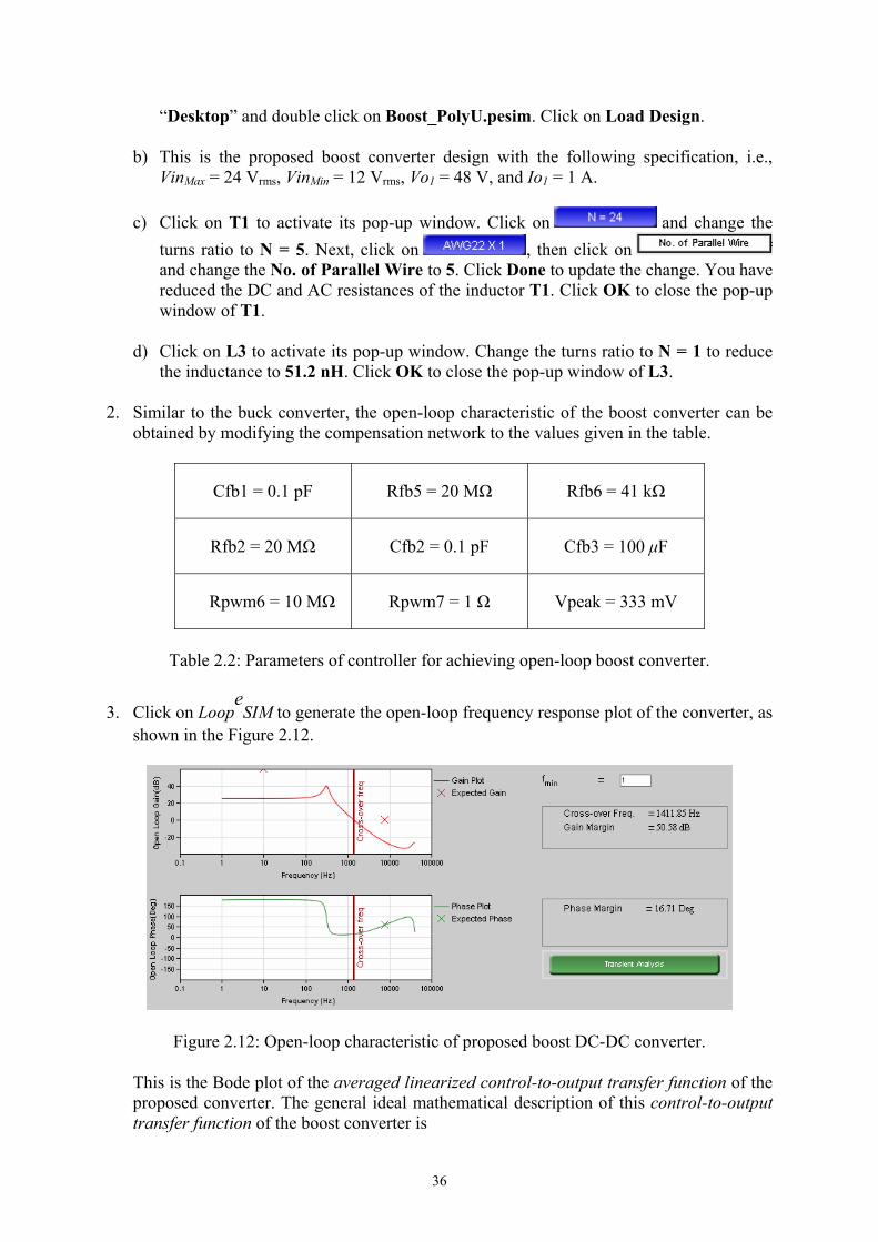
3. Click on LoopeSIM to generate the open-loop frequency response plot of the converter, as
shown in the Figure 2.12.
Figure 2.12: Open-loop characteristic of proposed boost DC-DC converter.
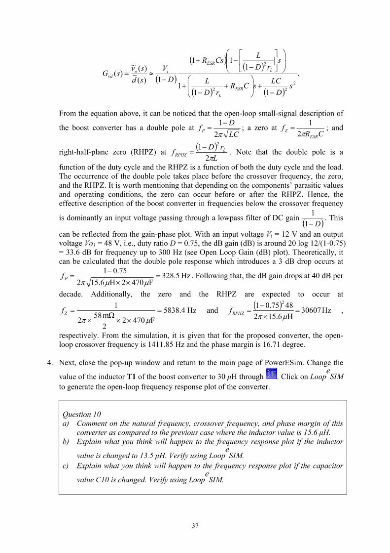
This is the Bode plot of the averaged linearized control-to-output transfer function of the proposed converter. The general ideal mathematical description of this control-to-output transfer function of the boost converter is
37
( )
( )( )
( ) ( )
.
111
111
1)(~)(~
)(2
22
2
sD
LCsCRrD
L
srD
LCsR
DV
sdsvsG
ESRL
LESR
iovd
−+⎟⎟
⎠
⎞⎜⎜⎝
⎛+
−+
⎟⎟⎠
⎞⎜⎜⎝
⎛⎥⎦
⎤⎢⎣
⎡
−−+
−≈=
From the equation above, it can be noticed that the open-loop small-signal description of
the boost converter has a double pole at LCDfP π2
1−= ; a zero at
CRf
ESRZ π2
1= ; and
right-half-plane zero (RHPZ) at ( )L
rDf LRPHZ π2
1 2−= . Note that the double pole is a
function of the duty cycle and the RHPZ is a function of both the duty cycle and the load. The occurrence of the double pole takes place before the crossover frequency, the zero, and the RHPZ. It is worth mentioning that depending on the components’ parasitic values and operating conditions, the zero can occur before or after the RHPZ. Hence, the effective description of the boost converter in frequencies below the crossover frequency
is dominantly an input voltage passing through a lowpass filter of DC gain ( )D−11 . This
can be reflected from the gain-phase plot. With an input voltage Vi = 12 V and an output voltage Vo1 = 48 V, i.e., duty ratio D = 0.75, the dB gain (dB) is around 20 log 12/(1-0.75) = 33.6 dB for frequency up to 300 Hz (see Open Loop Gain (dB) plot). Theoretically, it can be calculated that the double pole response which introduces a 3 dB drop occurs at
Hz5.328F4702H6.152
75.01=
××−
=μμπPf . Following that, the dB gain drops at 40 dB per
decade. Additionally, the zero and the RHPZ are expected to occur at
Hz4.5838F4702
2m582
1=
××Ω
×=
μπZf and ( ) Hz30607
H6.1524875.01 2
=×−
=μπRPHZf ,
respectively. From the simulation, it is given that for the proposed converter, the open-loop crossover frequency is 1411.85 Hz and the phase margin is 16.71 degree.
4. Next, close the pop-up window and return to the main page of PowerESim. Change the
value of the inductor T1 of the boost converter to 30 μH through . Click on LoopeSIM
to generate the open-loop frequency response plot of the converter.
Question 10 a) Comment on the natural frequency, crossover frequency, and phase margin of this
converter as compared to the previous case where the inductor value is 15.6 μH. b) Explain what you think will happen to the frequency response plot if the inductor
value is changed to 13.5 μH. Verify using LoopeSIM.
c) Explain what you think will happen to the frequency response plot if the capacitor
value C10 is changed. Verify using LoopeSIM.
38
5. Close the pop-up window and reset the inductor T1 to 15.6 μH and the capacitor C10 to “470u F 80 Vdc 58 mΩ 105°C 5000 hrs 16x30x mm LXV NCC 20%”. Generate the open-loop frequency response plot of the converter. At the top of the pop-up window, change the output current to Io1 = 4 A. Click Recalculate to refresh the plot under the new output current setting. Compare this frequency response plot with the one originally generated with Io1 = 1 A. Notice the deviation in crossover frequency and phase margin in the frequency response characteristic. This reflects that unlike the buck converter, the open-loop characteristic of the boost converter in CCM varies with different operating loads. Moreover, it has an RHPZ that moves with the load. This may affect the stable control of the boost converter since compensation network designed for a specific load may inject instability when the RHPZ changes when a different load is used.
6. You have completed Exercise 4. Do not close the Loop Analysis pop-up window. Reset
the output current back to Io1 = 1 A. Proceed to Exercise 5 using the same converter platform.
2.3.5 Exercise 5 This exercise aims to familiarize student the typical closed-loop characteristic of the boost DC-DC converters with the voltage mode control. 1. First of all, set the capacitance range of Cfb1, Cfb2, and Cfb3 to 0.01 pf (minimim) and
10 mf (maximum), and resistance range of Rfb2 and Rfb6 to 1 Ω (minimum) and 20 MΩ (maximum). The setting allows the computer simulation to search for the optimal compensation network within the preset ranges of capacitance and resistance.
2. Set the Expected DC Gain to > 70 dB, the Expected Phase Margin to > 60 Deg, and
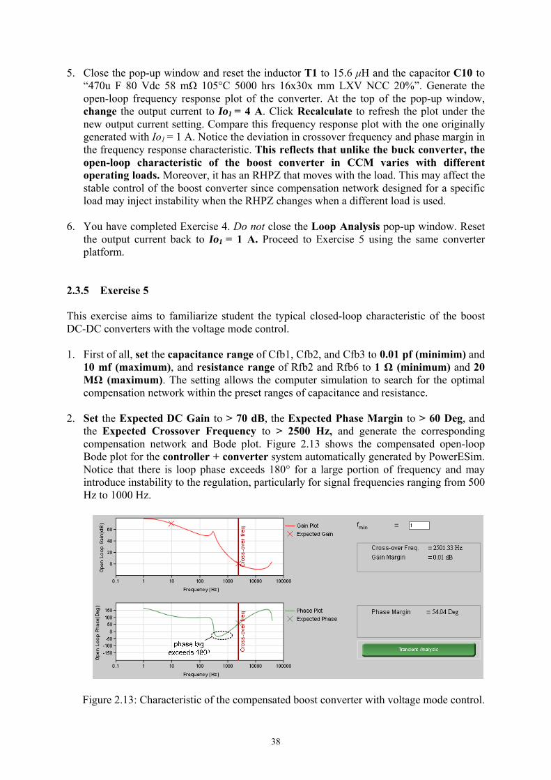
the Expected Crossover Frequency to > 2500 Hz, and generate the corresponding compensation network and Bode plot. Figure 2.13 shows the compensated open-loop Bode plot for the controller + converter system automatically generated by PowerESim. Notice that there is loop phase exceeds 180° for a large portion of frequency and may introduce instability to the regulation, particularly for signal frequencies ranging from 500 Hz to 1000 Hz.
Figure 2.13: Characteristic of the compensated boost converter with voltage mode control.

39
3. Next, click on Transient Analysis. Change the load current waveform by modifying Frequency, t0, t1, t2, …, and t7 to values as shown in Figure 2.14.
Figure 2.14: Load current waveform for the compensated boost converter.
4. Click on Apply to update the settings and to regenerate the transient waveforms (see Figure 2.15). The response of the output voltage is not particularly fast and stable. To stabilize the regulation, it is necessary to keep the loop phase to within 180° (ideal) and 120° (practical) for all frequencies below the crossover frequency.
Figure 2.15: Transient response of the boost converter with voltage mode control.
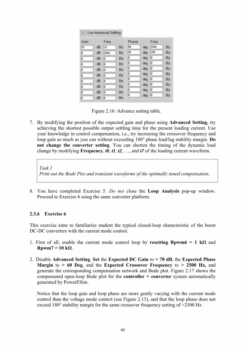
5. Click on Loop Analysis. Next, click on and then check on Use Advanced Setting, and modify the setting according to Figure 2.16.
6. Click on Automatic Compensation.
Question 11 a) Observe and comment on the change of the Bode plot. b) Do you think the transient response will be stable? Why? Verify your answer.
40
Figure 2.16: Advance setting table. 7. By modifying the position of the expected gain and phase using Advanced Setting, try
achieving the shortest possible output settling time for the present loading current. Use your knowledge in control compensation, i.e., try increasing the crossover frequency and loop gain as much as you can without exceeding 180° phase lead/lag stability margin. Do not change the converter setting. You can shorten the timing of the dynamic load change by modifying Frequency, t0, t1, t2, …, and t7 of the loading current waveform.
Task 1 Print out the Bode Plot and transient waveforms of the optimally tuned compensation.
8. You have completed Exercise 5. Do not close the Loop Analysis pop-up window.
Proceed to Exercise 6 using the same converter platform. 2.3.6 Exercise 6 This exercise aims to familiarize student the typical closed-loop characteristic of the boost DC-DC converters with the current mode control. 1. First of all, enable the current mode control loop by resetting Rpwm6 = 1 kΩ and
Rpwm7 = 10 kΩ. 2. Disable Advanced Setting. Set the Expected DC Gain to > 70 dB, the Expected Phase
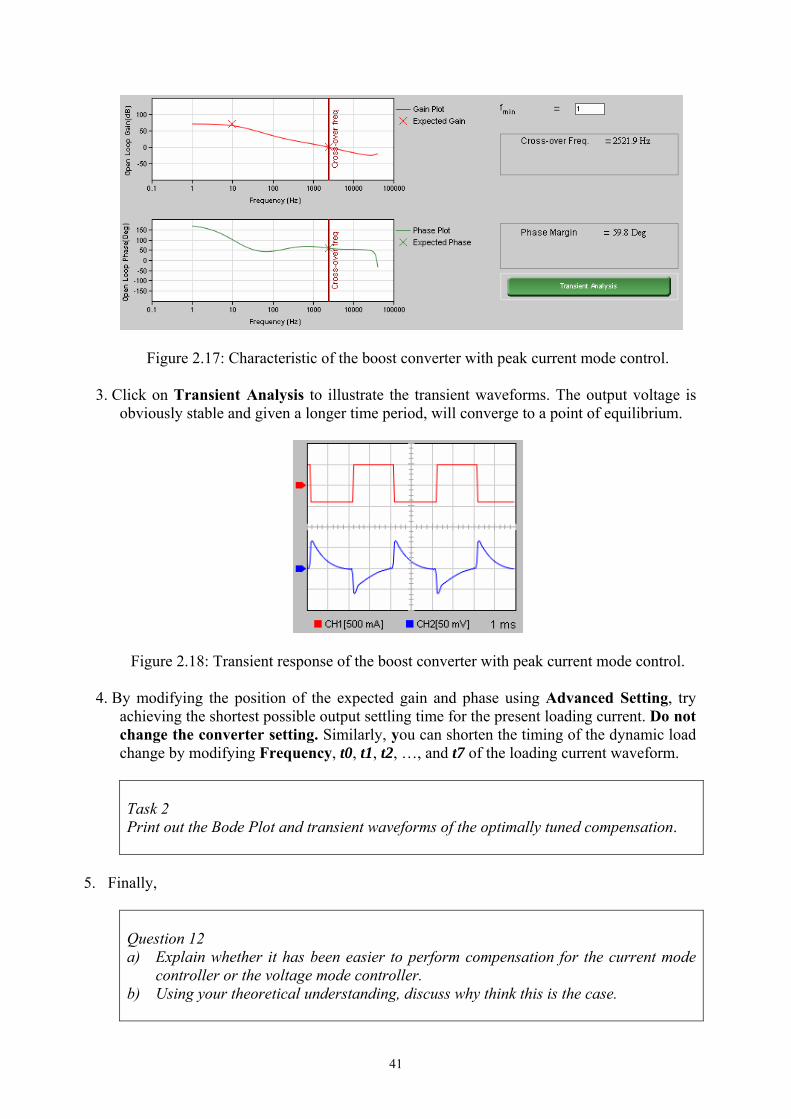
Margin to > 60 Deg, and the Expected Crossover Frequency to > 2500 Hz, and generate the corresponding compensation network and Bode plot. Figure 2.17 shows the compensated open-loop Bode plot for the controller + converter system automatically generated by PowerESim.
Notice that the loop gain and loop phase are more gently varying with the current mode control than the voltage mode control (see Figure 2.13), and that the loop phase does not exceed 180° stability margin for the same crossover frequency setting of >2500 Hz.
41
Figure 2.17: Characteristic of the boost converter with peak current mode control.
3. Click on Transient Analysis to illustrate the transient waveforms. The output voltage is obviously stable and given a longer time period, will converge to a point of equilibrium.
Figure 2.18: Transient response of the boost converter with peak current mode control.
4. By modifying the position of the expected gain and phase using Advanced Setting, try achieving the shortest possible output settling time for the present loading current. Do not change the converter setting. Similarly, you can shorten the timing of the dynamic load change by modifying Frequency, t0, t1, t2, …, and t7 of the loading current waveform.
Task 2 Print out the Bode Plot and transient waveforms of the optimally tuned compensation.
5. Finally,
Question 12 a) Explain whether it has been easier to perform compensation for the current mode
controller or the voltage mode controller. b) Using your theoretical understanding, discuss why think this is the case.

42
2.4 Assignment Submit a complete report answering all questions posed in the exercises. Attach all related theoretical proofs and simulated waveforms from the PowerESim. 2.5 References [1] E. Rogers, “Understanding buck power stages in switchmode power supplies”, Application Report SLVA057,
Texas Instruments, Mar. 1999. [2] E. Rogers, “Understanding boost power stages in switchmode power supplies”, Application Report SLVA061,
Texas Instruments, Mar. 1999. [3] R. Ridley, “Current mode or voltage mode?”, in Switching Power Magazine, pp. 4-9, Oct 2000. [4] R. Mammano, “Switching Power Supply Topology: Voltage Mode vs. Current Mode”, Design Note DN-62,
Unitrode, Jun. 1994. [5] L. Dixon, “Average current mode control of switching power supplies”, Application Note U-140, Unitrode,
1999.
43
Laboratory 3
Properties of Magnetic Devices
3.1 Objectives 1. To study how different parameters, i.e., physical dimensions, windings, core choices etc.,
affect the properties of magnetic devices, using the Magnetic Builders toolbox in the PowerESim package.
2. To understand the different aspects of practical inductors and transformers in power
supply industry. 3.2 Introduction Magnetic components (transformers and inductors) are a necessary part of power supply circuits. These magnetic devices come in many shapes, designs, winding arrangements, and properties etc., to cater for different applications. The application of transformers in switch mode power supplies is mainly to provide voltage/current amplitude conversion of high frequency pulses as well as for isolating the electrical circuit. The application of inductor in switch mode power supply, on the other hand, is for storing of electrical energy in the form of magnetic field and for filtering of high frequency ripple. The general structure of transformers and inductors are similar in the sense that both are constructed as coil(s) of conducting material (typically copper wire) that are wrapped around core(s) of either air or ferromagnetic material. Core materials with a higher permeability than air confine the magnetic field closely to the inductor, thereby increasing the inductance. In fact, the magnetic core is a major component influencing the characteristics of the inductor/transformer, with the most important factors being:
1. the geometry of the magnetic core; 2. the amount of air gap in the magnetic circuit; 3. the magnetic core material (especially permeability and hysteresis); and 4. the temperature of the core.
3.2.1 Common Types of Magnetic Core Shape The following figures show the common types of core shape used in the magnetic devices in the power supply industry.
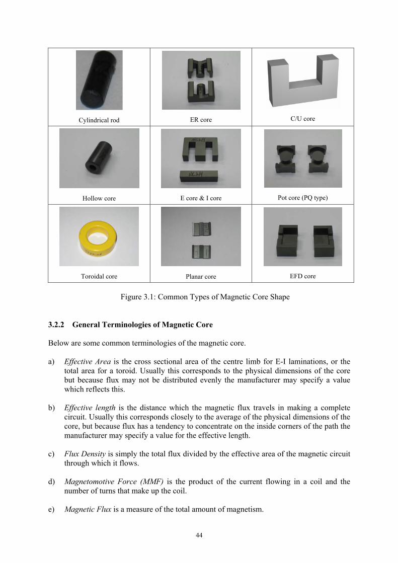
44
Cylindrical rod
ER core
C/U core
Hollow core
E core & I core
Pot core (PQ type)
Toroidal core
Planar core
EFD core
Figure 3.1: Common Types of Magnetic Core Shape
3.2.2 General Terminologies of Magnetic Core Below are some common terminologies of the magnetic core. a) Effective Area is the cross sectional area of the centre limb for E-I laminations, or the
total area for a toroid. Usually this corresponds to the physical dimensions of the core but because flux may not be distributed evenly the manufacturer may specify a value which reflects this.
b) Effective length is the distance which the magnetic flux travels in making a complete
circuit. Usually this corresponds closely to the average of the physical dimensions of the core, but because flux has a tendency to concentrate on the inside corners of the path the manufacturer may specify a value for the effective length.
c) Flux Density is simply the total flux divided by the effective area of the magnetic circuit
through which it flows. d) Magnetomotive Force (MMF) is the product of the current flowing in a coil and the
number of turns that make up the coil. e) Magnetic Flux is a measure of the total amount of magnetism.
45
f) Permeability is defined as the ratio of the flux density to the magnetic field strength, and is determined by the type of material within the magnetic field, i.e., the core material.
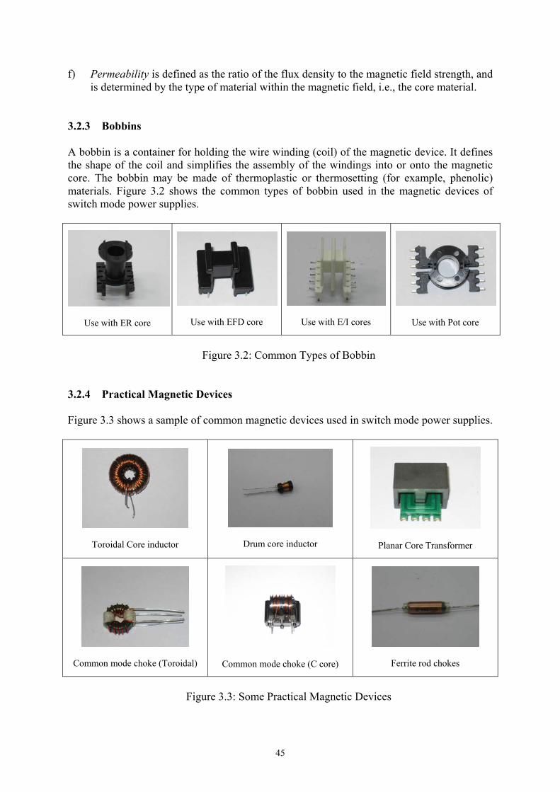
3.2.3 Bobbins A bobbin is a container for holding the wire winding (coil) of the magnetic device. It defines the shape of the coil and simplifies the assembly of the windings into or onto the magnetic core. The bobbin may be made of thermoplastic or thermosetting (for example, phenolic) materials. Figure 3.2 shows the common types of bobbin used in the magnetic devices of switch mode power supplies.
Use with ER core
Use with EFD core
Use with E/I cores
Use with Pot core
Figure 3.2: Common Types of Bobbin
3.2.4 Practical Magnetic Devices Figure 3.3 shows a sample of common magnetic devices used in switch mode power supplies.
Toroidal Core inductor
Drum core inductor
Planar Core Transformer
Common mode choke (Toroidal)
Common mode choke (C core)
Ferrite rod chokes
Figure 3.3: Some Practical Magnetic Devices

46
3.3 Exercises 3.3.1 Exercise 1 This exercise aims to familiarize students the effect of the inductor’s winding turns N and copper wire thickness on the magnetic and resistance property of the inductor. 1. Log in to PowerESim. 2. Click on Magnetic Builder to activate the platform. 3. Set Number of Secondary Windings to 0. Click OK to update the change. 4. At the Allowance for gap portion, check on No to select a core structure that has no air
gap. With the number of winding turns being set to N = 10, write down the value of the inductor, the DC resistance, and the ac resistance in the blanks provided below.
N = 10; Inductor L: _________ H; Rdc = ________ Ω; Rac = ________ Ω.
5. Now, set N = 5. Write down the respective parameters in the blanks below.
N = 5; Inductor L: _________ H; Rdc = ________ Ω; Rac = ________ Ω.
6. Next, set N = 20. Write down the respective parameters in the blanks below and answer
the following questions.
N = 20; Inductor L: _________ H; Rdc = ________ Ω; Rac = ________ Ω.
Question 1 a) Did L increase or decrease when N decreases? Why is this so? What is the
relationship of L and N? b) The DC resistance Rdc changes almost proportionally with the change of N. Explain
why this happens using your understanding on the resistive property of the inductor.c) The AC resistance increases with the increment of N. Why? Explain using your
understanding of the relationship of the AC resistance with the skin effect and proximity effect. Additionally, explain why AC resistance increases more quickly than the DC resistance for any increment in turning ratio.

47
7. Set winding turns back to N = 10. The copper wire used currently is “0.828 mm 155deg POLYON155 Triple Coated AWG21 Magnet Wire SHELHAV”. Click on
and change the wire to “1.593 mm 155deg POLYON155 Triple Coated AWG15 Magnet Wire SHELHAV”. This copper wire is almost twice as thick as the previous one. Write down the value of the inductor, the DC resistance, and the ac resistance in the blanks provided below.
N = 10; Inductor L: _________ H; Rdc = ________ Ω; Rac = ________ Ω.
8. Compare these results with that recorded in (4) and answer the following questions.
Question 2 a) Does the change of copper wire thickness affect the inductance? b) Explain why the overall DC resistance Rdc drop when a thicker copper wire is used?c) On the other hand, why did the AC resistance increase when a thicker copper wire
is used? Explain the phenomenon using the relationship of eddy current and proximity effect versus thickness of copper wire.
9. Next, change the wire to “0.4166 mm 180deg ISOBOND Heavy Coated AWG27
Magnet Wire SHELHAV”. This copper wire is almost half as thick as the original one in (4). Also, change the number of parallel wire to 5 by clicking . Write down the value of the inductor, the DC resistance, and the ac resistance in the blanks provided below.
N = 10; Inductor L: _________ H; Rdc = ________ Ω; Rac = ________ Ω.
10. Compare these results with that recorded in (4). You can see that both DC and AC
resistances are reduced by paralleling thinner copper wires. This technique is commonly practiced in application.
Question 3 a) Explain why this paralleling of thin wires technique works in reducing both AC and
DC resistances? b) Why is it important to minimize the AC and DC resistances of the inductor in switch
mode power supply?
11. Close the pop-up window to return to the main page of PowerEsim. You have completed
Exercise 1. Proceed to Exercise 2.

48
3.3.2 Exercise 2 This exercise aims to familiarize students the effect of various parameters on the power loss property of the inductor. 1. Click on Magnetic Builder to activate the platform. 2. Set Number of Secondary Windings to 0. Click OK to update the change. 3. At the Allowance for gap portion, keep the check on Yes. This means that you have
selected a core structure with air gap. Click on to see the estimated power loss for the present inductor. Copy down the parameters in the blanks provided in Table 3.1 under the column “Inductor 1”. Close the Estimate Power Loss platform.
Parameters Inductor 1 Inductor 2 Bm (mT) N (turns) Inductor value (H) Gap Length (mm) Total loss (W) Core loss (W) Conduction loss (W) Fringing and leakage loss (W)
Table 3.1: Power loss of the inductor with different inductances.
4. Change winding turns to N = 20. Click on to see the estimated power loss for this inductor. Copy down the parameters in the blanks provided in Table 3.1 under the column “Inductor 2”. Close the Estimate Power Loss platform. Check the magnetic flux density Bm value at the top of the Magnetic Builder platform. Set the turns back to N = 10. Proceed to answer the following questions.
Question 4 a) Why is there no change of inductance value when N change? (Hint: observe airgap
length). b) We know that the conduction loss is composed of losses due to the AC and DC
resistances, and the fringing and leakage loss is due to the leakage and fringing fluxes. State what core loss is contributed by?
c) According to Table 3.1, did the fringing and leakage flux loss increase or decrease when N increases? Explain why this happens?
d) According to Table 3.1, did the overall core loss increase or decrease when N increases? Explain why this happens? (Hint: N affects the level of magnetic flux).

49
5. Fill in the blanks of the second column in Table 3.2, i.e., “Idc = 0 A, Vpos = 100 V, fs = 100 kHz”, with the parameters recorded in Table 3.1 of the column “Inductor 1”. These values signify the various inductor losses when there is no DC current passing through the inductor.
Parameters Idc = 0 A,
Vpos = 100 V, fS = 100 kHz.
Idc = 3 A, Vpos = 100 V, fS = 100 kHz.
Idc = 0 A, Vpos = 100 V, fS = 1 MHz.
Idc = 0 A, Vpos = 50 V,
fS = 100 kHz.Bm (mT) Total loss (W) Core loss (W) Conduction loss (W) Fringing and leakage loss (W)
Table 3.2: Power loss of the inductor when operated under different conditions.
6. Click on . Change the DC current to Idc = 3 A. Click Apply to refresh the computation. Copy down the various losses in the blanks provided in Table 3.2 of the third column, i.e., “Idc = 3 A, Vpos = 100 V, fs = 100 kHz”. These are the inductor losses when it is operated with a DC current of 3 A. Close the Estimate Power Loss platform. Check the magnetic flux density Bm value at the top of the Magnetic Builder platform. Proceed to answer the following questions.
Question 5 a) Is there any change in the fringing and leakage loss? Why? b) Was the change in the conduction loss due to AC resistances or DC resistances? c) Why is there an increment in core loss when the inductor is operated with a DC
current? (Hint: refer to BH curve operating condition)
7. Click on . Change the DC current back to Idc = 0 A. Set the operating frequency to fS = 1 MHz. Click Apply to refresh the computation. Copy down the various losses in the blanks provided in Table 3.2 of the fourth column, i.e., “Idc = 0 A, Vpos = 100 V, fs = 1 MHz”. These are the inductor losses when it is operated at 1 MHz. Close the Estimate Power Loss platform. Check the magnetic flux density Bm. Make a comparison between the results obtained for this operating condition and the ones in column two, i.e., “Idc = 0 A, Vpos = 100 V, fs = 100 kHz”. Proceed to answer the following questions.
Question 6 a) Did the increment of the operating frequency increases or decreases the various
categories of losses? b) Was this what you expect? If not, what could be the contribution to these
discrepancies? (Hint: operating frequency affects the Bm value )

50
8. Click on . Change the frequency back to fS = 100 kHz. Set the applied voltage to Vpos = 50 V. Click Apply to refresh the computation. Copy down the various losses in the blanks provided in Table 3.2 of the last column, i.e., “Idc = 0 A, Vpos = 50 V, fs = 100 kHz”. These are the inductor losses when it is applied with a voltage of Vpos = 50 V. Close the Estimate Power Loss platform. Check the magnetic flux density Bm. Make a comparison between the results obtained for this operating condition and the ones in column two, i.e., “Idc = 0 A, Vpos = 100 V, fs = 100 kHz”. Proceed to answer the following questions.
Question 7 a) Did the reduction in the magnitude of the applied voltage increases or decreases the
various categories of losses? b) Was this what you expect? If not, what could be the contribution to these
discrepancies? (Hint: applied voltage affects the Bm value )
9. Close the pop-up window to return to the main page of PowerEsim. You have completed
Exercise 2. Proceed to Exercise 3. 3.3.3 Exercise 3 This exercise aims to familiarize students the effect of fringing and leakage fluxes on the power loss property of the inductor. 1. Click on Magnetic Builder to activate the platform. 2. Set Number of Secondary Windings to 0. Click OK to update the change.
3. At the Allowance for gap portion, keep the check on Yes. Click on and set the inductance as 40 μH. At the bottom right of Magnetic Builder platform, set the Overall
bobbin thickness to 0.25 mm. Click on to see the estimated power loss for the present inductor. Copy down the parameters in the blanks provided in Table 3.1 under the column “0.25 mm”. Close the Estimate Power Loss platform.
Bobbin Thickness (mm) 0.25 0.50 1.00 2.00 2.25 2.50 2.75 4.00 Total loss (W) Core loss (W) Conduction loss (W) Fringing/leakage loss (W)
Table 3.3: Power loss of the inductor for different bobbin thicknesses.
4. Change the Overall bobbin thickness to 0.5 mm. Check the estimated power loss. Copy
the parameters in the blanks of Table 3.3 under the column “0.5 mm”. Repeat the steps for bobbin thicknesses of 1.00 mm, 2.00 mm, 2.25 mm, 2.50 mm. 2.75 mm, and 4.00 mm.

51
5. Observe the loss due to fringing and leakage flux in Table 3.3. Make a comparison between the results obtained for different bobbin thicknesses. Proceed to answer the following questions.
Question 8 a) Did you expect fringing and leakage loss to reduce as bobbin thickness increases
from 0.25 mm to 2.25 mm? Why do you think this happens? b) Is there an optimal bobbin thickness in terms of fringing and leakage flux loss? If
so, why does the fringing and leakage flux loss increase after this optimal bobbin thickness?
c) Do you think there will be fringing and leakage flux loss if there is no airgap in the magnetic core structure? If yes, what is this loss due to? Verify using PowerESim.
3.4 Assignment Submit a complete report answering all questions posed in the exercises. Attach all related theoretical proofs and simulated waveforms from the PowerESim.

52
Laboratory 4
Design and Construction of a 50 W Flyback Converter
4.1 Objectives 1. To perform a thorough circuit design of a flyback converter using the PowerESim
package. 2. To perform the hardware construction and circuit evaluation of the flyback converter. 4.2 Introduction The flyback converter is a DC-to-DC converter with a galvanic isolation between the input source and the output source(s). More precisely, the flyback converter is a buck-boost converter with its inductor being split to form a transformer, so that the voltage conversion ratios are multiplied and that electrical isolation is provided. The typical use of this converter is in low power applications (< 250 W), namely, in low-power switch-mode power supplies like cell-phone charger, standby power supply in PCs, main PC supplies; and in high voltage supply for the CRT in TVs and monitors. The aim of this laboratory exercise is to familiarize students on the use of PowerESim to design a power supply base on the flyback converter topology, and also to provide students the opportunity to go through both the process of designing and constructing a complete power supply product with compliance to the common industrial standard.
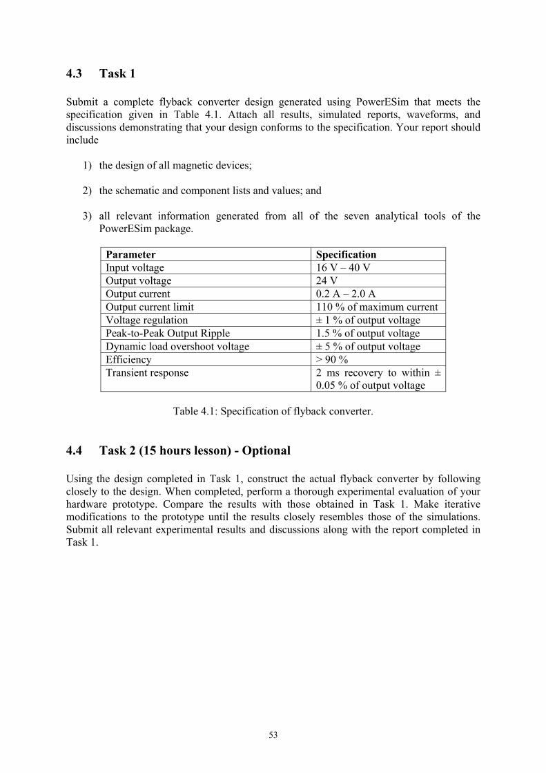
53
4.3 Task 1 Submit a complete flyback converter design generated using PowerESim that meets the specification given in Table 4.1. Attach all results, simulated reports, waveforms, and discussions demonstrating that your design conforms to the specification. Your report should include
1) the design of all magnetic devices; 2) the schematic and component lists and values; and
3) all relevant information generated from all of the seven analytical tools of the
PowerESim package.
Parameter Specification Input voltage 16 V – 40 V Output voltage 24 V Output current 0.2 A – 2.0 A Output current limit 110 % of maximum current Voltage regulation ± 1 % of output voltage Peak-to-Peak Output Ripple 1.5 % of output voltage Dynamic load overshoot voltage ± 5 % of output voltage Efficiency > 90 % Transient response 2 ms recovery to within ±
0.05 % of output voltage
Table 4.1: Specification of flyback converter. 4.4 Task 2 (15 hours lesson) - Optional Using the design completed in Task 1, construct the actual flyback converter by following closely to the design. When completed, perform a thorough experimental evaluation of your hardware prototype. Compare the results with those obtained in Task 1. Make iterative modifications to the prototype until the results closely resembles those of the simulations. Submit all relevant experimental results and discussions along with the report completed in Task 1.