Embed Size (px)
Citation preview
Fabrication of (K,Na)NbO3 Lead-Free Piezoceramic Microrod Arraysby Sol–Gel Processing with Micromachined Silicon Templates
Ying Xu, Dawei Liu, Fengping Lai, Yuhua Zhen, and Jing-Feng Li*,w
State Key Laboratory of New Ceramics and Fine Processing, Department of Materials Science and Engineering,Tsinghua University, 100084 Beijing, China
A microfabrication process combining sol–gel processing andsilicon micromolding was proposed to fabricate microrod arraysof K0.5Na0.5NbO3 (KNN) lead-free piezoelectric ceramics. Byultraviolet lithography and inductively coupled plasma deep re-active ion etching, a Si mold with a regular array of columnarcavities was micromachined, and then filled with KNN sol, fol-lowed by pyrolysis and annealing treatment. By optimizing theprocessing conditions, KNN ceramic microrod arrays of 15 lmlateral width, 30 lm height, and 70 lm spacing were produced,which were identified as perovskite phase structure by X-raydiffraction.
I. Introduction
PIEZOELECTRIC ceramics that couple electrical and mechanicalenergy are widely used for electromechanical transducers,
such as underwater hydrophones and ultrasonic imagingprobes.1–3 Connectivity piezoelectric composites, in which pie-zoceramic rods are embedded in a polymeric matrix, show manyadvantages over bulk piezoelectric ceramics, such as loweracoustic impedance (Z), higher coupling coefficient (kt), higherpiezoelectric voltage output coefficient (g33), lower mechanicalquality factor (Qm), dielectric loss (tgd), and better design flex-ibility.1–5 Many studies have been conducted so far to develop afabrication process related to 1–3 piezoelectric composites, par-ticularly piezoceramic microrod arrays having a microscale lat-eral width and high aspect ratio, which are required for high-frequency and high-resolution medical imaging.1,6–13 Recently,the fabrication technology of such microrod arrays has becomeincreasingly important not only for developing piezoceramic/polymer composites but also for other novel functional materi-als such as multiferroic composites containing piezoceramic rodarrays embedded in a ferromagnetic medium.14
This paper reports the method of combining silicon micro-machining and sol–gel processing to fabricate ceramic microrodarrays, by which (K0.5Na0.5)NbO3 (abbreviated as KNN here-after) microrod arrays of 15 mm lateral width, 30 mm height, and70 mm spacing were obtained. The KNN rods were formed in-side a micromachined silicon mold that was filled with KNN solsolution, being similar to an impregnating sol process reportedby Kakimoto et al.15 Although the present process can be ap-plied to other ceramic materials including widely used lead-con-taining Pb(Zr,Ti)O3-based piezoelectric ceramics, KNN wasselected in the present study mainly because it is one of thepromising candidates of lead-free piezoelectric ceramics, whichare being extensively studied currently.16–18Additionally, the
KNN-based ceramic of the 1–3-type structure may meet spe-cific requirements for imaging transducers and is more favorablethan most Pb(Zr,Ti)O3-based ceramics in this field because of itslower dielectric properties and lower mechanical quality factor.
II. Experimental Procedure
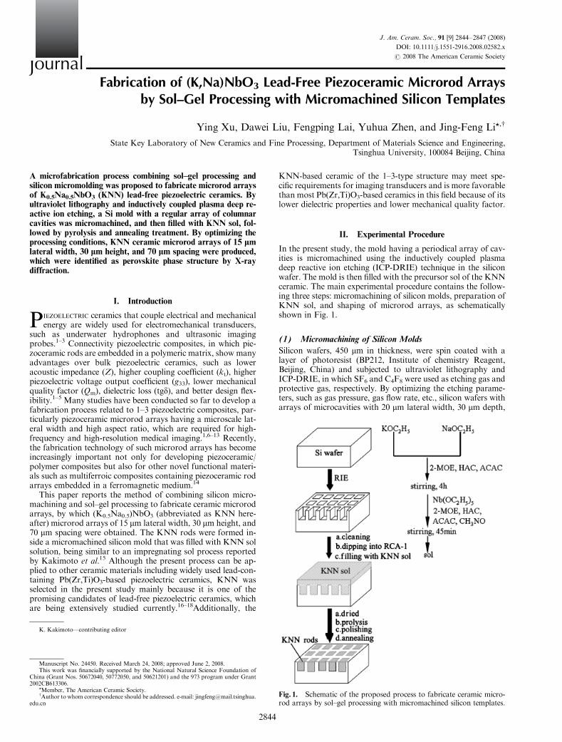
In the present study, the mold having a periodical array of cav-ities is micromachined using the inductively coupled plasmadeep reactive ion etching (ICP-DRIE) technique in the siliconwafer. The mold is then filled with the precursor sol of the KNNceramic. The main experimental procedure contains the follow-ing three steps: micromachining of silicon molds, preparation ofKNN sol, and shaping of microrod arrays, as schematicallyshown in Fig. 1.
(1) Micromachining of Silicon Molds
Silicon wafers, 450 mm in thickness, were spin coated with alayer of photoresist (BP212, Institute of chemistry Reagent,Beijing, China) and subjected to ultraviolet lithography andICP-DRIE, in which SF6 and C4F8 were used as etching gas andprotective gas, respectively. By optimizing the etching parame-ters, such as gas pressure, gas flow rate, etc., silicon wafers witharrays of microcavities with 20 mm lateral width, 30 mm depth,
Fig. 1. Schematic of the proposed process to fabricate ceramic micro-rod arrays by sol–gel processing with micromachined silicon templates.
K. Kakimoto—contributing editor
This work was financially supported by the National Natural Science Foundation ofChina (Grant Nos. 50672040, 50772050, and 50621201) and the 973 program under Grant2002CB613306.
*Member, The American Ceramic Society.wAuthor to whom correspondence should be addressed. e-mail: [email protected].
edu.cn
Manuscript No. 24450. Received March 24, 2008; approved June 2, 2008.
Journal
J. Am. Ceram. Soc., 91 [9] 2844–2847 (2008)
DOI: 10.1111/j.1551-2916.2008.02582.x
r 2008 The American Ceramic Society
2844
and 60 mm spacing were successfully machined. A detailed de-scription of ultraviolet lithography and ICP-DRIE can be foundelsewhere.9–11,19
(2) Preparation of KNN Sol
Proper amounts of sodium ethoxide (NaOC2H5) solution andpotassium ethoxide (KOC2H5) solution, which were prepared byreacting solid Na and K with ethanol (99.7%), were mixed in asolvent of 2-methoxyethanol (2-MOE) to form alkoxide solu-tion. By adding 2 mL acetic acid (HAC) and 1 mL acetylacetone(ACAC) as stabilizer and chelating ligand, respectively, the mix-ture was stirred and heated at 1201C for 4 h to stabilize thedouble-metal alkoxides. A stoichiometric amount of niobiumpentaethoxide [Nb(OC2H5)5], 2 mL 2-MOE, 2 mL HAC, 1 mLACAC, and 1 mL formamide were then added to the solution,which was stirred for another 45 min and distilled to the re-quired concentration. By this method, two kinds of sol (0.167and 0.3M KNN sol) with a stoichiometric ratio of 1:1:2 (K, Na,Nb) were prepared. The sol was then aged for 2 weeks for sub-sequent processes.
(3) Shaping of KNN Arrays
Completely filling the micromachined silicon mold with KNNsol is the key point of the present process. Several methods weretested in the present study to improve the filling quality, andeventually the cavities of the silicon mold were successfully filledwith KNN sol. The detailed process will be described later to-gether with the experimental results. Finally, the filled mold wassubjected to pyrolysis at 4001C and annealing treatment at8301C to crystallize the ceramic rods, as in the case of fabricat-ing sol–gel-derived KNN films.20
The crystal structure of the KNN arrays was investigated byX-ray diffraction (XRD, D/max-RB, Rigaku, Tokyo, Japan)using CuKa radiation. The surface morphology and the cross-sectional microstructure of the arrays were inspected by scan-ning electron microscopy (SEM, JSM6460, JEOL Ltd., Tokyo,Japan).
III. Results and Discussion
The micromachined silicon mold was cleaned before the fillingprocess, using acetone and a mixture of concentrated sulfuric acid(98%) and hydrogen peroxide solution (30%) with a volume ratioof 2:1. As it was difficult to completely fill the mold, RCA-1 so-lution, which was composed of ammonia solution (25%), hydro-gen peroxide solution (30%), and deionized water with a volumeratio of 1:1:5, was introduced to improve its surface wettabilityafterward. Moreover, a vacuum condition was created by a me-chanical pump to enhance the filling speed; only 10 min wereneeded for the sol to fill the mold and be dried in vacuum,whereas this period was at least 40 min in open atmosphere.
Table I summarizes the preparation conditions of samples,with molds treated with RCA-1 solution or not treated, andfilled in vacuum or in open atmosphere; for the vacuum-enhanced filling process, the sol concentration was also changedfor comparison.
To observe the cross-sections, the filled samples after anneal-ing treatment were cleaved mechanically with a diamond cutter,in which KNN rods were damaged to some extent. Generallyspeaking, the quality of the filling and rod formation were in-
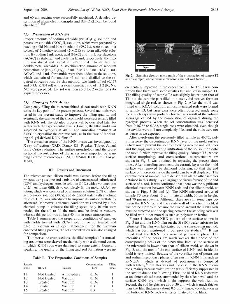
crementally improved in the order from T1 to T5. It was con-firmed that there were some cavities left unfilled in sample T1.The filling quality of sample T2 was slightly better than that ofT1, but the ceramic part filled in a cavity did not yet form anintegrated single rod, as shown in Fig. 2. After the mold wasrinsed with RCA-1 solution, almost integrated rods were formedin sample T3, but large gaps were often observed inside somerods. Such gaps were probably formed as a result of the volumeshrinkage caused by the combustion of organics during thepyrolysis process. When the sol concentration was increasedfrom 0.167M to 0.3M, single rods were obtained, even thoughthe cavities were still not completely filled and the rods were notas dense as we expected.
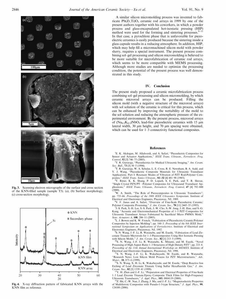
After pyrolyzing the previously filled sample at 4001C, pol-ishing away the discontinuous KNN layer on the mold surface(which might prevent the sol from flowing into the unfilled holesand the gaps) and repeating infiltration of the sol solution ontothe mold further improve the filling quality. Sample T5 , whosesurface morphology and cross-sectional microstructure areshown in Fig. 3, was obtained by repeating the process threetimes. After annealing treatment, the ceramic layer on the moldsurface was removed by diamond polishing, so that the endsurface of microrods inside the mold can be well displayed. Theceramic rods of sample T5 are denser than all the other samplesobtained in this study. By enlarging the circumference of the endsurface of a rod, it was confirmed that there was no significantchemical reaction between KNN rods and the silicon mold, asshown in Figs. 3 (b) and (c). The KNN microrod arrays ofsample T5 were about 15 mm in lateral width, 30 mm in height,and 70 mm in spacing. Although there are still some gaps be-tween the KNN rod and the cavity wall of the silicon mold, itwill not be a problem because the silicon around the KNN rodsmust be removed and the spacing between the standing rods willbe filled with other materials such as polymer or ferrite.
Figure 4 shows the XRD pattern of the surface shown inFig. 3 (a) and the KNN film on the Si (100) wafer substrate forreference. The film was fabricated by the spin-coating method,which has been mentioned in our previous studies.20,21 It wasfound that the KNN rods were of perovskite phase. Theintensities of the peaks are much weaker than those of thecorresponding peaks of the KNN film, because the surface ofthe microrods is lower than that of silicon mold, as shown inFig. 3, and the area of the end surface of KNN rods inside themold is very limited. Because of the volatilization of potassiumand sodium, secondary phases often exist in KNN films such asK2Nb4O11, which is devoid of potassium as comparedwith KNbO3,
20 but this was not the case in the KNN micro-rods, mainly because volatilization was sufficiently suppressed inthe cavities due to the following. First, the filled KNN rods wereat an almost closed state, surrounded by the silicon wall and thesurface KNN layer, which might suppress the volatilization.Second, the rod heights are about 30 mm, which is much thickerthan the film thickness (about 0.5 mm); hence, volatilization inthe bulk-like KNN rods was lesser relative to the films.
Table I. The Preparation Conditions of Samples
Sample
name RCA-1 Pressure
Concentration
(M)
Filling
times
T1 Not treated Atmosphere 0.167 1T2 Not treated Vacuum 0.167 1T3 Treated Vacuum 0.167 1T4 Treated Vacuum 0.3 1T5 Treated Vacuum 0.3 3
Fig. 2. Scanning electron micrograph of the cross section of sample T2as an example, whose ceramic microrods are not well formed.
September 2008 Fabrication of (K,Na)NbO3 Lead-Free Piezoceramic Microrod Arrays 2845
A similar silicon micromolding process was invented to fab-ricate Pb(Zr,Ti)O3 ceramic rod arrays in 1999 by one of thepresent authors together with his coworkers, in which a powderprocess and glass-encapsulated hot-isostatic pressing (HIP)method were used for the forming and sintering processes.9–11
In that case, a pyrochlore phase that is unfavorable for piezo-electric ceramics is easily produced because the sintering inside aglass capsule results in a reducing atmosphere. In addition, HIP,which may help fill a micromachined silicon mold with powderslurry, requires a special instrument. The present process com-bining sol–gel processing and silicon micromolding is believed tobe more suitable for microfabrication of ceramic rod arrays,which seems to be more compatible with MEMS processing.Although more studies are needed to optimize the processingcondition, the potential of the present process was well demon-strated in this study.
IV. Conclusion
The present study proposed a ceramic microfabrication processcombining sol–gel processing and silicon micromolding, by whichceramic microrod arrays can be produced. Filling thesilicon mold (with a negative structure of the microrod arrays)with sol solution of the ceramic is critical for this process, whichcan be enhanced by improving the wettability of the mold tothe sol solution and reducing the atmospheric pressure of the ex-perimental environment. By the present process, microrod arraysof (Na0.5K0.5)NbO3 lead-free piezoelectric ceramics with 15 mmlateral width, 30 mm height, and 70 mm spacing were obtained,which can be used for 1–3 connectivity functional composites.
References
1E. K. Akdogan, M. Allahverdi, and A. Safari, ‘‘Piezoelectric Composites forSensor and Actuator Applications,’’ IEEE Trans. Ultrason., Ferroelectr. Freq.Control, 52 [5] 746–75 (2005).
2T. R. Gururaja, ‘‘Piezoelectrics for Medical Ultrasonic Imaging,’’ Am. Ceram.Soc. Bull., 73 [5] 50–5 (1994).
3T. R. Gururaja, W. A. Schulze, L. E. Cross, R. E. Newnham, B. A. Auld, andY. J. Wang, ‘‘Piezoelectric Composite Materials for Ultrasonic TransducerApplications. Part I: Resonant Modes of Vibration of PZT Rod-Polymer Com-posites,’’ IEEE Trans. Sonics Ultrason., SU-32 [4] 481–98 (1985).
4T. Ritter, K. K. Shung, P. D. Lopath, S. E. Park, and T. R. Shrout,‘‘Single Crystal PZN/PT—Polymer Composites for Ultrasound Transducer Ap-plications,’’ IEEE Trans. Ultrason., Ferroelectr. Freq. Control, 47 [4] 792–800(2000).
5W. A. Smith, ‘‘The Role of Piezocomposites in Ultrasonic Transducers’’;pp. 755–66. Proceedings of the 1989 IEEE Ultrasonics Symposium. Institute ofElectrical and Electronics Engineers, Piscataway, NJ, 1989.
6V. F. Janas and A. Safari, ‘‘Overview of Fine-Scale Piezoelectric Ceramic/Polymer Composite Processing,’’ J. Am. Ceram. Soc., 78 [11] 2445–55 (1995).
7J.-S. Park, S.-H. Lee, S.-S. Park, J.-W. Cho, S.-W. Jung, J.-H. Han, and S.-G.Kang, ‘‘Acoustic and Electromechanical Properties of 1–3 PZT Composites forUltrasonic Transducer Arrays Fabricated by Sacrificial Micro PMMA Mold,’’Sens. Actuators A, 108, 206–11 (2003).
8L. J. Bowen and K. W. French, ‘‘Fabrication of Piezoelectric Ceramic/PolymerComposites by Injection Molding’’; pp. 160–3. Proceeding of the 8th IEEE Inter-national Symposium on Applications of Ferroelectrics. Institute of Electrical andElectronics Engineers, Piscataway, NJ, 1992.
9S. N. Wang, J.-F. Li, R. Watanabe, and M. Esashi, ‘‘Fabrication of Lead Zir-conate Titanate Microrods for 1–3 Piezocomposites Using Hot Isostatic Pressingwith Silicon Molds,’’ J. Am. Ceram. Soc., 82 [1] 213–5 (1999).
10S. N. Wang, J.-F. Li, R. Watanabe, K. Minami, and M. Esashi, ‘‘NovelProcessing of High Aspect Ratio 1–3 Structures of High Density PZT’’; pp. 223–8.Proceeding of the 11th Annual International Workshop on MEMES. Institute ofElectrical and Electronics Engineers, Piscataway, NJ, 1998.
11S. N. Wang, J.-F. Li, K. Wakabayashi, M. Esashi, and R. Watanabe,‘‘Research News: Lost Silicon Mold Process for PZT Microstructures,’’ Adv.Mater., 10, 873–6 (1999).
12S. N. Wang, X. H. Li, K. Wakabayashi, and M. Esashi, ‘‘Deep Reactive IonEtching of Lead Zirconate Titanate Using Sulfur Hexafluoride Gas,’’ J. Am.Ceram. Soc., 82 [5] 1339–41 (1999).
13Y. H. Zhen and J.-F. Li, ‘‘Preparation and Electrical Properties of Fine-Scale1–3 Lead Zirconic Titanate/Epoxy Composite Thick Films for High-FrequencyUltrasonic Transducers,’’ J. Appl. Phys., 103, 0804119 (2008).
14Z. Shi, C.-W. Nan, J. Zhang, J. Ma, and J.-F. Li, ‘‘Magnetoelectric Propertiesof Multiferroic Composites with Pseudo-1-3-type Structure,’’ J. Appl. Phys., 99,124108 (2006).
Fig. 4. X-ray diffraction pattern of fabricated KNN arrays with theKNN film as reference.
Fig. 3. Scanning electron micrographs of the surface and cross sectionof the KNN-filled sample (sample T5). (a), (b) Surface morphology;(c) cross-section morphology.
2846 Journal of the American Ceramic Society—Xu et al. Vol. 91, No. 9

15K. Kakimoto, T. Imura, Y. Fukui, M. Kuno, K. Yamagiwa, T. Mitsuoka,and K. Ohbayashi, ‘‘Processing of Piezoelectric (Li,Na,K)NbO3 Porous Ceramicsand (Li,Na,K)NbO3/KNbO3 Composites,’’ Jpn. J. Appl. Phys., 46, 7089–93 (2007).
16C. Eric, ‘‘Lead Free at Last,’’ Nature, 432 [7013] 24–5 (2004).17Y. Saito, H. Takao, T. Tani, T. Nonoyama, K. Takatori, T. Homma, T. Nagaya,
and M. Nakamura, ‘‘Lead-Free Piezoceramics,’’ Nature, 432 [7013] 84–7 (2004).18J.-F. Li and K. Wang, ‘‘Ferroelectric and Piezoelectric Properties of
Fine-Grained Na0.5K0.5NbO3 Lead-Free Piezoelectric Ceramics Prepared bySpark Plasma Sintering,’’ J. Am. Soc., 89 [2] 706–9 (2006).
19H. Jansen, H. Gardeniers, M. Boer, M. Elwenspoek, and J. Fluitman, ‘‘ASurvey on the Reactive Ion Etching of Silicon inMicrotechnology,’’ J. Micromech.Microeng., 6, 14–28 (1996).
20F. P. Lai and J.-F. Li, ‘‘Sol–Gel Processing of Lead-Free (Na,K)NbO3 Fer-roelectric Films,’’ J. Sol–Gel Sci. Tech., 42, 287–92 (2007).
21W. Gong, J.-F. Li, X. C. Chu, Z. L. Gui, and L. T. Li, ‘‘Preparation andCharacterization of Sol–Gel Derived (100)-Textured Pb(Zr,Ti)O3 Thin Films: PbOSeeding Role in the Formation of Preferential Orientation,’’ Acta Mater., 52,2787–93 (2004). &
September 2008 Fabrication of (K,Na)NbO3 Lead-Free Piezoceramic Microrod Arrays 2847