Embed Size (px)
Citation preview
NASA/TM-2003-212501
Field Programmable Gate Array for Implementation of Redundant Advanced Digital Feedback Control K.D. King Marshall Space Flight Center, Marshall Space Flight Center, Alabama
June 2003 i
https://ntrs.nasa.gov/search.jsp?R=20030065651 2018-07-10T08:53:40+00:00Z

The NASA STI Program Ofice...in Profile
Since its founding, NASA has been dedicated to the advancement of aeronautics and space science. The NASA Scientific and Technical Information (STI) Program Office plays a key part in helping NASA maintain this important role.
The NASA STI Program Office is operated by Langley Research Center, the lead center for NASA’s scientific and technical information. The NASA STI Program Office provides access to the NASA STI Database, the largest collection of aeronautical and space science STI in the world. The Program Office is also NASA’s institutional mechanism for disseminating the results of its research and development activities. These results are published by NASA in the NASA STI Report Series, which includes the following report types:
TECHNICAL PUBLICATION. Reports of completed research or a major significant phase of research that present the results of NASA programs and include extensive data or theoretical analysis. Includes compilations of significant scientific and technical data and information deemed to be of continuing reference value. NASA’s counterpart of peer-reviewed formal professional papers but has less stringent limitations on manuscript length and extent of
I graphic presentations.
TECHNICAL MEMORANDUM. Scientific and technical findings that are preliminary or of specialized interest, e.g., quick release reports, working papers, and bibliographies that contain minimal annotation. Does not contain extensive analysis.
CONTRACTOR REPORT. Scientific and I technical findings by NASA-sponsored
contractors and grantees.
CONFERENCE PUBLICATION. Collected papers from scientific and technical conferences, symposia, seminars, or other meetings sponsored or cosponsored by NASA.
SPECIAL PUBLICATION. Scientific, technical, or historical information from NASA programs, projects, and mission, often concerned with subjects having substantial public interest.
TECHNICAL TRANSLATION. English-language translations of foreign scientific and technical material pertinent to NASA’s mission.
Specialized services that complement the STI Program Office’s diverse offerings include creating custom thesauri, building customized databases, organizing and publishing research results.. .even providing videos.
For more information about the NASA STI Program Office, see the following:
Access the NASA STI Program Home Page at http://w wwsti.nasa.gov
E-mail your question via the Internet to help@ sti.nasa.gov
Fax your question to the NASA Access Help Desk at (301) 621-0134
Telephone the NASA Access Help Desk at (301) 621-0390
Write to: NASA Access Help Desk NASA Center for Aerospace Information 7 12 1 Standard Drive Hanover, MD 21076-1320
NASA /T~-2003-212501
Field Programmable Gate Array for Implementation of Redundant Advanced Digital Feedback Control K.D. King Marshall Space Flight Center, Marshall Space Flight Center, Alabama
National Aeronautics and Space Administration
Marshall Space Flight Center MSFC, Alabama 35812
June 2003
TABLE OF CONTENTS
1. INTRODUCTION .......................................................................................................................... 1
2. BACKGROUND ....................... . .................................................................................................... 2
3. APPROACH ................................................................................................................................... 3
4. DESIGN DESCRIPTION ............................................................................................................... 5
4.1 Serial Receiver Interface ......................................................................................................... 6 4.2 Motor Control Logic ............................................................................................................... 7 4.3 Serial Transmitter Interface ............................................ ............................... .......................... 9
5. APPLICATIONS AND OBSERVATIONS ..... .. . . . . . . . . .. . . . . . .. . . . . . . .. . . . . . ... . . . .. .. . . . .. .. . . . . . . . . . . .. .. . . . . . . . . . .. . .. . . 10
6. SUMMARY .................................................................................................................................... 1 1
... 111

LIST OF ACRONYMS
A2D
ccw
I cw
FPGA
R A D
PID
PWM
rad
I I SEU
SRAM
TED
TMR
TTL
UART
VHDL
analog to digital
counterclockwise
clockwise
field programmable gate array
independent research and development
proportional-integral-derivative (controller)
pulse-width modulation
radiation
single event upset
static random access memory
thermal electric device
triple-modular redundancy
transistor transistor logic
universal asynchronus receiver/transmitter
very high-speed integrated circuit hardware description language
l
.

LIST OF FIGURES
1. Breadboard configuration ........................................................................................................... 4
2. FPGA block diagram .................................................................................................................. 5
3. Constant velocity mode profile ................................................................................................... 8
4. Position mode profile .................................................................................................................. 8
V

NOMENCLATURE
e
Kd
I Ki
KP
I
n
0
t
I
I
I V
error
derivative constant
integral constant
proportional constant
current sample period
output to motor
time
velocity
vii .l

TECHNICAL MEMORANDUM
FIELD PROGRAMMABLE GATE ARRAY FOR IMPLEMENTATION OF REDUNDANT ADVANCED DIGITAL FEEDBACK CONTROL
1. INTRODUCTION
The goal of this effort was to develop a digital motor controller using field programmable gate arrays (FPGAs). This is a more rugged approach than a conventional microprocessor digital controller. FPGAs typically have a higher radiation (rad) tolerance than both the microprocessor and memory required for a conventional digital controller. Furthermore, FPGAs can typically operate at higher speeds. (While speed is usually not an issue for motor controllers, it can be for other system controllers.) Other than motor power, only a 3.3-V digital power supply was used in the controller; no analog bias supplies were used. Since most of the circuit was implemented in the FPGA, no additional parts were needed other than the power transistors to drive the motor. The benefits that FPGAs provide over conventional designs-lower power and fewer parts-allow for smaller packaging and reduced weight and cost.

2. BACKGROUND
Motor control systems are currently being employed at Marshall Space Flight Center for both propulsion and microgravity experiments. NASA also utilizes motor-driven systems for reusable vehicle flight control surfaces. Some motor-driven systems are used in propulsion for nozzle and fuel valve positioning. It is obvious that fault-tolerance and redundancy techniques must be used where control surface or propulsion system malfunctions could result in loss of mission, vehicle, or crew.
Usually, the experimenter accepts risk without the benefit of fault-tolerant techniques even though they would provide a higher probability of mission success. Smaller, cheaper solutions are normally used for experiments because of budget constraints. If redundancy could be provided at very little extra cost, it would greatly benefit the experimenter.
2 ~
3. APPROACH
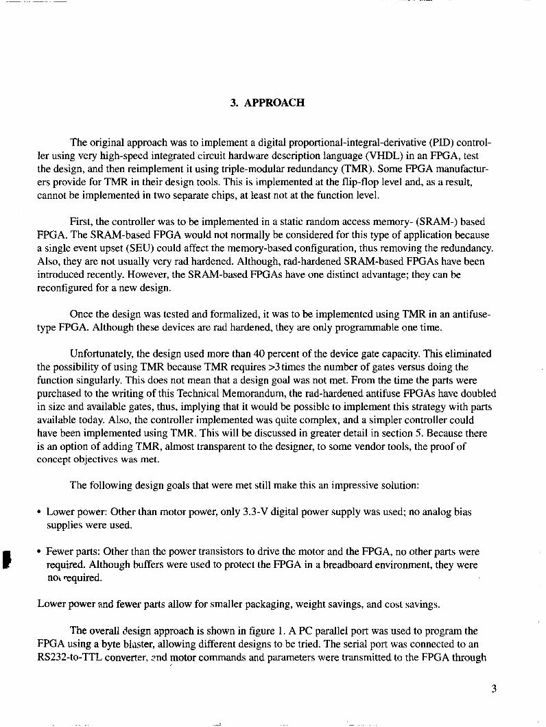
The original approach was to implement a digital proportional-integral-derivative (PID) control- ler using very high-speed integrated circuit hardware description language (VHDL) in an FPGA, test the design, and then reimplement it using triple-modular redundancy (TMR). Some FPGA manufactur- ers provide for TMR in their design tools. This is implemented at the flip-flop level and, as a result, cannot be implemented in two separate chips, at least not at the function level.
First, the controller was to be implemented in a static random access memory- (SRAM-) based FPGA. The SRAM-based FPGA would not normally be considered for this type of application because a single event upset (SEU) could affect the memory-based configuration, thus removing the redundancy. Also, they are not usually very rad hardened. Although, rad-hardened SRAM-based FPGAs have been introduced recently. However, the SRAM-based FPGAs have one distinct advantage; they can be reconfigured for a new design.
Once the design was tested and formalized, it was to be implemented using TMR in an antifuse- type FPGA. Although these devices are rad hardened, they are only programmable one time.
Unfortunately, the design used more than 40 percent of the device gate capacity. This eliminated the possibility of using TMR because TMR requires >3 times the number of gates versus doing the function singularly. This does not mean that a design goal was not met. From the time the parts were purchased to the writing of this Technical Memorandum, the rad-hardened antifuse FPGAs have doubled in size and available gates, thus, implying that it would be possible to implement this strategy with parts available today. Also, the controller implemented was quite complex, and a simpler controller could have been implemented using TMR. This will be discussed in greater detail in section 5. Because there is an option of adding TMR, almost transparent to the designer, to some vendor tools, the proof of concept objectives was met.
The following design goals that were met still make this an impressive solution:
Lower power: Other than motor power, only 3.3-V digital power supply was used; no analog bias supplies were used.
Fewer parts: Other than the power transistors to drive the motor and the FPGA, no other parts were required. Although buffers were used to protect the FPGA in a breadboard environment, they were noi required.
Lower power and fewer parts allow for smaller packaging, weight savings, and cost savings.
The overall design approach is shown in figure 1. A PC parallel port was used to program the FPGA using a byte blaster, allowing different designs to be tried. The serial port was connected to an RS232-to-TTL converter, 2nd motor commands and parameters were transmitted to the FPGA through
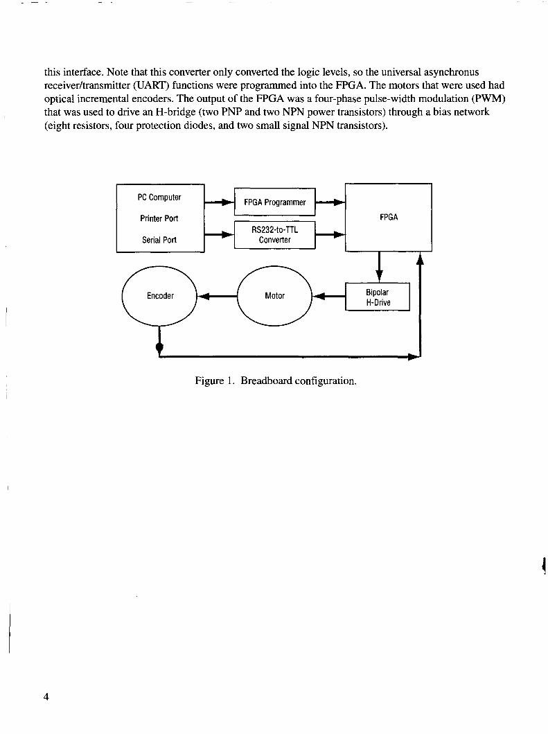
this interface. Note that this converter only converted the logic levels, so the universal asynchronus receiverhransmitter (UART) functions were programmed into the FPGA. The motors that were used had optical incremental encoders. The output of the FPGA was a four-phase pulse-width modulation (PWM) that was used to drive an H-bridge (two PNP and two NPN power transistors) through a bias network (eight resistors, four protection diodes, and two small signal NPN transistors).
I
I I i I
FPGAProgrammer PC Computer
Printer Port I I FPGA
I I
7
Figure 1. Breadboard configuration.
4
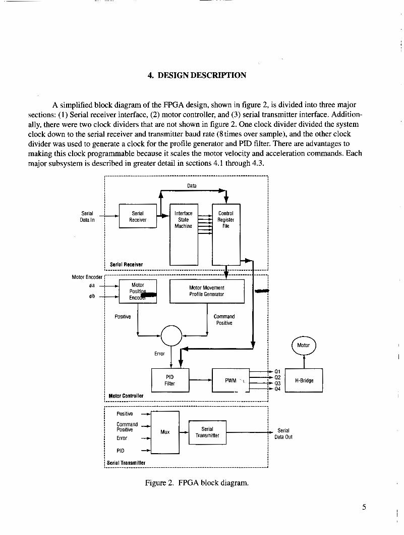
4. DESIGN DESCRIPTION
A simplified block diagram of the FPGA design, shown in figure 2, is divided into three major sections: ( 1) Serial receiver interface, (2) motor controller, and (3) serial transmitter interface. Addition- ally, there were two clock dividers that are not shown in figure 2. One clock divider divided the system clock down to the serial receiver and transmitter baud rate (8 times over sample), and the other clock divider was used to generate a clock for the profile generator and PID filter. There are advantages to making this clock programmable because it scales the motor velocity and acceleration commands. Each major subsystem is described in greater detail in sections 4.1 through 4.3.
I ! I Q1
Q2 Q3 Q4
Motor Y H-Bridge
i Positive Serial i Error Transmitter Data Out
Figure 2. FPGA block diagram.
5

4.1 Serial Receiver Interface
Although not the focus of this project, a good overview of the registers and commands provides insight concerning how the motor controller section works, so it will be described first.
The serial receiver interface consists of a serial receiver, interface state machine, and a register file, shown in figure 2. The serial receiver simply detects the RS232 start bit and shifts the serial data stream into an 8-bit parallel word. The interface state machine takes the first word into the register file as an address. When the second word is received, it generates a latch enable for the selected register in the register file. The format is as follows:
First word=Address of register.
Second word=Data for selectec.
To provide for a common starting point, register addresses start with 1 and a register address of zero generates a reset to the sequence generator; thus, sending two consecutive zeros will always reset the sequence generator.
The register file contains the following nine registers with their functions:
(1) Kp: This is the 8-bit proportional gain used by the PID controller.
(2) Kd: This is the 8-bit differential gain used by the PID controller. - (3) Ki: This is the %bit iilLcgra1 gain used by the PID contl-.
(4) Most significant byte of the end position: See list item 5.
(5) Least significant byte of the end position: When in position mode, the motor profile generator uses the least significant byte of the end position. Registers 4 and 5 form a 16-bit position for the generator to stop and hold the motor.
(6) Start velocity: This 8-bit value is used by the profile generator for the starting velocity. It is used in both position and constant velocity modes.
(7) End velocity: This value is used by the profile generator as the end velocity; acceleration is stopped when this velocity is reached. End velocity is also used in both position and velocity modes.
(8) Acceleration: This value is used by the profile generator in both position and velocity modes. In the position mode, it is also used as the deacceleration value when slowing down to stop at the end position.
6

(9) Control register: This register controls the operation of the motor drive. The bits in this word have the following meanings:
Bit &Direction: l=clockwise (CW) and O=counterclockwise (CCW). Bit I-Position mode: l=move to and hold constant position and O=maintain constant
Bit 2-Start: When set to 1, all registers are loaded and motor drive logic may start. Bit 3-Stop: When set to 1, the profile generator and PID are reset and the PWM output is disabled. Bits 4 and 5-Serial transmit data select: Serial transmit data select chooses the transmit data to PID output, motor encoder position, profile generator, or error signal. The serial transmit output was primarily used for debugging, troubleshooting, and evaluation. Bit &Polarity: If polarity is set to 1, it reverses the polarity of the PWM. If the motor is wired backwards, reversing the PWM polarity removes the requirement of reversing the motor leads.
velocity.
4.2 Motor Control Logic
The motor control logic consists of four primary components: (1) Motor position encoder, (2) profile generator, (3) PID filter, and (4) the PWM.
4.2.1 Motor Position Encoder
The motor position encoder accepted two biphase signals from the motor’s optical encoder. The two signals form a binary Gray code (00, 01, 1 1, 10,OO.. .). Note that only one bit of the code changes (0 to 1 or 1 to 0) at a time. In this manner, bouncing can be detected. Also, from this code the direction of rotation can be determined. The position encoder used a 16-bit counter and a four-state state machine.
4.2.1.1 Operation. The state machine remembers the current state of the inputs. If the inputs change to a valid CCW direction, then the counter is decremented If the inputs change to a valid CW direction, then the counter is incremented. It is important that the state machine runs at a higher clock rate than the bounce frequency of the optical encoders in the motor. A frequency of 2.4576 MHz was chosen because it is a higher clock rate and is evenly divisible to give a standard PC RS232 baud rate.
The above circuit was originally designed with Schmitt-trigger buffers (74HC 14) to reduce the effect of bouncing and slow rise times from the motor’s optical encoders. They were later removed to prove that the state machine did not require them. Although the encoder was not affected by the removal of the Schmitt-trigger buffers, good engineering practices would indicate their use regardless.
4.2.2 Profile Generator
The profile generator has two modes of operation: (1) Constant velocity mode and (2) position mode. In both modes, the generator provides the desired motor position to the error amplifier. The constant velocity mode is the simpler of the two modes and will be explained first.
7
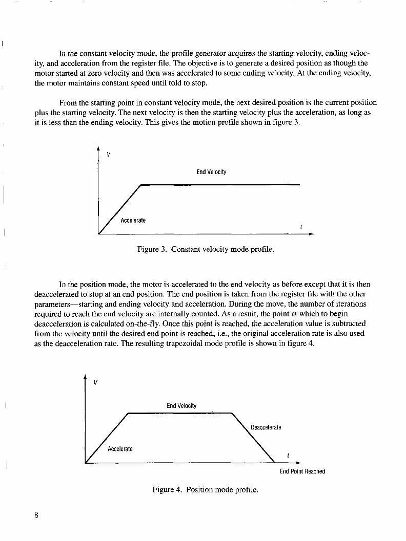
In the constant velocity mode, the profile generator acquires the starting velocity, ending veloc- ity, and acceleration from the register file. The objective is to generate a desired position as though the motor started at zero velocity and then was accelerated to some ending velocity. At the ending velocity, the motor maintains constant speed until told to stop.
From the starting point in constant velocity mode, the next desired position is the current position plus the starting velocity. The next velocity is then the starting velocity plus the acceleration, as long as it is less than the ending velocity. This gives the motion profile shown in figure 3.
t ' End Velocity
Accelerate
Figure 3. Constant velocity mode profile.
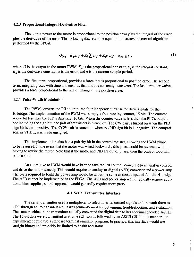
In the position mode, the motor is accelerated to the end velocity as before except that it is then deaccelerated to stop at an end position. The end position is taken from the register file with the other parameters-starting and ending velocity and acceleration. During the move, the number of iterations required to reach the end velocity are internally counted. As a result, the point at which to begin deacceleration is calculated on-the-fly. Once this point is reached, the acceleration value is subtracted
as the deacceleration rate. The resulting trapezoidal mode profile is shown in figure 4.
I from the velocity until the desired end point is reached; i.e., the original acceleration rate is also used
I ' End Velocity
End Point Reached
Figure 4. Position mode profile.
4.2.3 Proportional-Integral-Derivative Filter
The output power to the motor is proportional to the position error plus the integral of the error plus the derivative of the error. The following discrete time equation illustrates the control algorithm performed by the FPGA:
where 0 is the output to the motor PWM, Kp is the proportional constant, Ki is the integral constant, Kd is the derivative constant, e is the error, and n is the current sample period.
The first term, proportional, provides a force that is proportional to position error. The second term, integral, grows with time and ensures that there is no steady-state error. The last term, derivative, provides a force proportional to the rate of change of the position error.
4.2.4 Pulse-Width Modulation
The PWM converts the PID output into four independent transistor drive signals for the H-bridge. The implementation of the PWM was simply a free-running counter, 15 bits. The counter is one bit less than the PID’s data size, 16 bits. When the counter value is less than the PID’s output, not including the sign bit, one pair of transistors is turned on. The CW pair is turned on when the PID sign bit is zero, positive. The CCW pair is turned on when the PID sign bit is 1, negative. The compari- son, in VHDL, was made unsigned.
This implementation also had a polarity bit in the control register, allowing the PWM phase to be reversed. In the event that the motor was wired backwards, this phase could be reversed without having to rewire the motor. Note that if the motor and PID are out of phase, then the control loop will be unstable.
An alternative to PWM would have been to take the PID output, convert it to an analog voltage, and drive the motor directly. This would require an analog-to-digital (A2D) converter and a power amp. The parts required to build the power amp would be about the same as those required for the H-bridge. The A2D cannot be implemented in the FPGA. The A2D and power amp would typically require addi- tional bias supplies, so this approach would generally require more parts.
4.3 Serial nansmitter Interface
The serial transmitter used a multiplexer to select internal control signals and transmit them to a PC through an RS232 interface. It was primarily used for debugging, troubleshooting, and evaluation. The state machine in the transmitter actually converted the digital data to hexadecimal encoded ASCII. The 16-bit data were transmitted as four ASCII words followed by an ASCII CR. In this manner, the experimenter could use a standard terminal emulator program. In practice, this interface would use straight binary and probably be limited to health and status.
9

5. APPLICATIONS AND OBSERVATIONS
The two areas of this design that are very complex are as follows:
(1) Serial transmitter interface: This interface was required to support the general purpose design in a breadboard environment. In a more typical application-specific situation, this interface might be greatly simplified. For example, for a given motor, Ki, Kp, and Kd might be known, so in this case, there would be no reason for these parameters to be transmitted to the controller. For the same case, even the starting and maximum velocities might be constant. Also, the data would not need to be ASCII encoded hexadecimal.
I (2) Profile generator: The profile generator can operate in both constant velocity and position modes, making the module more complex. In a typical application, velocity or position might need to be controlled, but probably not both.
Even though TMR was not implemented with the devices selected, a specific application might lend itself to optimizations that would allow TMR even with smaller parts. Furthermore, FPGAs have doubled in size since these parts were purchased for this independent research and development. Because some VHDL compilers can implement TMR with a simple switch, the proof of concept is still valid.
Other applications might include thermal controls. Many space flight experiments require heaters or coolers. Because multiple mode profiles would not be required for a heater or cooler, a smaller device could be used and still be redundant. The H-drive used in this investigation could be used to drive a thermal electric device (TED). TEDs can heat or cool depending on the direction of current through the device.
~
I
Where redundancy is not required, there are many commercial applications that would benefit I from this as well. This design solution provides a cost effective means of saving power, weight, and size.
I 10

6. SUMMARY
It has been shown that a complex general purpose motor controller can be implemented in an FPGA. This controller was capable of position or constant velocity control. As a general purpose controller, it could communicate with a PC and accept mode profiles and control parameters. The entire controller, with the exception of a high-voltage current drive, was implemented in an FPGA. Some additional advantages of an all-FTGA solution follow:
Lower power: A classical analog solution using op-amps usually requires more power supply voltages-plus and minus bias voltages in addition to the motor power.
Fewer parts: A classical analog solution using op-amps would typically require more parts, including resistors and capacitors to set the gain and transfer function. Even the conventional digital solution requires more parts-a microprocessor, memory, interfaces, and glue logic.
N o additional software: The FPGA solution versus the conventional digital approach does not require any software. This can translate to quicker design turnaround and lower manpower required for main- taining the design throughout its life cycle.
The proof of concept shows a direct migration path to implementation in a rad-hardened, triple- modular redundant FPGA. Applications are high-reliability space flight systems, with cost savings that may make it possible for low-budget experiments to benefit from a higher probability of mission suc- cess. Additionally, terrestrial applications, which may not need the redundancy, could still benefit from the savings of cost, weight, and power.
11
REPORT DOCUMENTATION PAGE
1. AGENCY USE ONLY (Leave Blank) 2. REPORT DATE
June 2003
I Fom Approved OMB No. 0704-0188
3. REPORT TYPE AND DATES COVERED
Technical Memorandum
I
Public reporting burden for this collection of information is estimated to average 1 hour per response, including the time for reviewing instructions. searching existing data sources. gathering and maintaining the data needed, and cmpleting and reviewing the collection of information. Send comments regarding this burden estimate or any other aspect of this collection of information. includino sumstions lor reducino this burden. to Washinoton Headauallers Services. Directorate for Information Owration and R e o m . 1215 Jefferson
1. TITLE AND SUBTITLE
Field Programmable Gate Array for Implementation of Redundant Advanced Digital Feedback Control
5. FUNDING NUMBERS
i. AUTHORS
K.D. King
’. PERFORMING ORGANIZATION NAMES(S) AND ADDRESS(ES)
George C. Marshall Space Flight Center Marshall Space Flight Center, AL 358 12
8. PERFORMING ORGANIZATION
I NUMBER
1. SPONSORlNGIMONlTORlNG AGENCY NAME(S) AND ADDRESqES)
National Aeronautics and Space Administration Washington, DC 20546-0001
M-1076
10. SPONSORlNGMONlTORlNG AGENCY REPORT NUMBER
NASPSTM-2003-212501
14. SUBJECT TERMS
field programmable gate, array, digital, microprocessor, controller, radiation, motor, static, random, tnple-modular redundancy, serial, receiver, interface, generator 7. SECURITY CLASSIFICATION 18. SECURITY CLASSIFICATION 19. SECURITY CLASSIFICATION
OF REPORT OF THIS PAGE OF ABSTRACT
Unclassified Unclassified Unclassified
I
3. ABSTRACT (Maximum 200 words)
The goal of this effort was to develop a digital motor controller using field programmable gate arrays (FPGAs). This is a more rugged approach than a conventional microprocessor digital controller. FPGAs typically have higher radiation (rad) tolerance than both the microprocessor and memory required for a conventional digital controller. Furthermore, FPGAs can typically operate at higher speeds. (While speed is usually not an issue for motor controllers, it can be for other system controllers.) Other than motor power, only a 3.3-V digital power supply was used in the controller; no analog bias supplies were used. Since most of the circuit was implemented in the FPGA, no additional parts were needed other than the power transistors to drive the motor. The benefits that FPGAs provide over conventional designs-lower power and fewer parts-allow for smaller packaging and reduced weight and cost.
15. NUMBER OF PAGES
20 16. PRICE CODE
20. LIMITATION OF ABSTRACT
Unlimited