Embed Size (px)
Citation preview
L - -
RESEARCH ON DIGITAL
TRANSDUCER PRINCIPLES
Volume X.
THIN FILM TITANIUM DIOXIDE
BY CHEMICAL VAPOR DEPOSITION
CASE F ILE COP%
THE UNIVERSITY OF TEXAS
COLLEGE OF ENGINEERING
AUSTIN
https://ntrs.nasa.gov/search.jsp?R=19700001409 2018-06-13T09:59:11+00:00Z


RESEARCH ON D I G I T A L
TRANSDUCER P R I N C I P L E S
V o l u m e X.
T H I N F I L M TITANIUM D I O X I D E
BY CHEMICAL VAPOR D E P O S I T I O N
f o r the
NATIONAL AERONAUTICS AND SPACE ADMINISTRATION
GRANT NGL 44-012-043
C o v e r i n g t he Pe r iod
July 1, 1968 - D e c e m b e r 31, 1968
by
D a l e R . H a r b i s o n
H . L y n d o n T a y l o r
W i l l i a m H. H a r t w i g
T h e U n i v e r s i t y of T e x a s a t A u s t i n
A u s t i n , T e x a s 78712

Page intentionally left blank

PREFACE
The discont inuous V-I c h a r a c t e r i s t i c of t h i n f i l m MIS s t r u c -
t u r e s has been regarded a s p o t e n t i a l l y product ive of d i g i t a l t ransducer
ac t ion . The missing element i s an a c t i v e d i e l e c t r i c f i l m which responds
t o e x t e r n a l s t i m u l i . A t t h e o u t s e t , cons iderable research has been con-
ducted by t h e s e n i o r au thor with a view t o development of such "exot ic"
d i e l e c t r i c s . The j u s t i f i c a t i o n i s much broader , however, s i n c e new di -
e l e c t r i c f i lms a r e p o t e n t i a l l y u s e f u l i n many microe lec t ronics and i n t e -
g r a t e d c i r c u i t s a r e a s .
Thin d i e l e c t r i c f i l m formation by chemical vapor depos i t ion ( C V D )
remains t o be i n v e s t i g a t e d a s thoroughly as s p u t t e r i n g , evapora t ion , and
oxida t ion . Chemical vapor depos i t ion o f f e r s s e v e r a l advantages over o t h e r
methods of d i e l e c t r i c f i l m growth. Titanium dioxide has promise a s a di-
e l e c t r i c m a t e r i a l i n i n t e g r a t e d c i r c u i t s because of i t s high d i e l e c t r i c
cons tan t . Present emphasis on microe lec t ronics and i n t e g r a t e d c i r c u i t s in -
d i c a t e s a need f o r new ma te r i a l s t o improve t h e performance of e x i s t i n g
devices and t o a i d i n new developments. High d i e l e c t r i c constant m a t e r i a l s
o f f e r t h e advantage of h ighe r capaci tance without t h e n e c e s s i t y f o r l a r g e r
a reas o r t h i n n e r f i l m s which l e a d t o p i n holes and device f a i l u r e . This
d i s s e r t a t i o n i n v e s t i g a t e s us ing CVD of t i t a n i u m organometal l ics t o form
t h i n f i lms of Ti0 followed by a s tudy of t h e phys i ca l and e l e c t r i c a l prop- 2 )
e r t i e s of t h e f i l m s .
The work descr ibed i n t h i s r epo r t rece ived p a r t i a l support from
NASA Grant NGL 44-012-043, and from t h e NSF (Grant GK 1395) and t h e J o i n t
Serv ices E lec t ron ic s Program r rant A~-AFosR-766-76).
i v
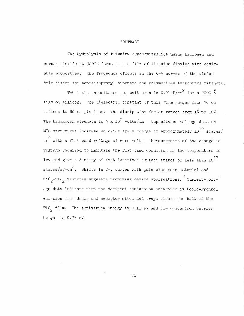
The hydro lys is of t i t an ium organometal l ics us ing hydrogen and
carbon dioxide a t 900°C forms a t h i n f i l m of t i t an ium dioxide with d e s i r -
ab le p r o p e r t i e s . The frequency e f f e c t s i n t h e C-V curves of t he d i e l ec -
t r i c d i f f e r f o r t e t r a i s o p r o p y l t i t a n a t e and polymerized t e t r a b u t y l t i t a n a t e .
2 0
The 1 kHz capaci tance pe r u n i t a r e a i s 0.2lyF/cm f o r a 2000 A
f i l m on s i l i c o n . The d i e l e c t r i c cons tan t of t h i s f i l m ranges from 50 on
s i l i c o n t o 80 on plat inum. The d i s s i p a t i o n f a c t o r ranges from 1% t o 10%.
The breakdown s t r e n g t h i s 5 x l o 5 volts/cm. Capacitance-voltage d a t a on
MIS s t r u c t u r e s i n d i c a t e an oxide space charge of approximately 1012 s t a t e s /
2 cm wi th a f la t -band vol tage of zero v o l t s . Measurements of t h e change i n
vol tage r equ i r ed t o maintain t h e f l a t band condi t ion a s t h e temperature i s
].owered g ive a dens i ty of f a s t i n t e r f a c e su r f ace s t a t e s of l e s s than 10 12
2 states/eV-cm . S h i f t s i n C-V curves wi th g a t e e l ec t rode m a t e r i a l and
SiO -Ti0 mixtures sugges ts promising device a p p l i c a t i o n s . Current-volt- 2 2
age d a t a i n d i c a t e t h a t t h e dominant conduction mechanism i s Poole-Frenkel
emission from donor and acceptor s i t e s and t r a p s wi th in t h e bulk of t h e
Ti0 f i lm . The a c t i v a t i o n energy i s 0 .11 eV and t h e conduction b a r r i e r 2
height i s 0.25 eVs
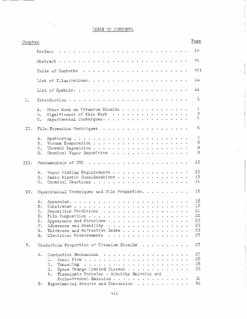
TABLE OF CONTENTS
Chapter Page
. . . . . . . . . . . . . . . . . . . . . . . . . . . Preface i v
. . . . . . . . . . . . . . . . . . . . . . . . . . . Abst rac t v i
. . . . . . . . . . . . . . . . . . . . . . Table of Contents v i i
. . . . . . . . . . . . . . . . . . . . . L i s t of I l l u s t r a t i o n s i x
. . . . . . . . . . . . . . . . . . . . . . . . L i s t of Symbols x i
I In t roduc t ion . . . . . . . . . . . . . . . . . . . . . . . . . 1 .
A Other Work on Titanium Dioxide . . . . . . . . . . . . . . 1 . B Signi f icance o f t h i s Work . . . . . . . . . . . . . . . . 3 . C Experimental Techniques . . . . . . . . . . . . . . . . . . 4 .
I1 . Film Formation Techniques . . . . . . . . . . . . . . . . . . 6
A . Spu t t e r ing . . . . . . . . . . . . . . . . . . . . . . . . 7 B . Vacuum Evaporation . . . . . . . . . . . . . . . . . . . . 8 C . Thermal Deposi t ion . . . . . . . . . . . . . . . . . . . . 9 D . Chemical Vapor Deposi t ion . . . . . . . . . . . . . . . . 9
. . . . . . . . . . . . . . . . . . . . . I11 . Fundamentals of CVD 1 3
. . . . . . . . . . . . . . . . A . Vapor P l a t i n g Requirements 1 3 . . . . . . . . . . . . . . . B . Basic Kine t ic Considerat ions 1 3
. . . . . . . . . . . . . . . . . . . . C . Chemical Reactions 1 4
. . . . . . . . . . IV . Experimental Techniques and Film P r o p e r t i e s 18
A . Apparatus . . . . . . . . B . Subs t r a t e s . . . . . . . C . Deposition Conditions .
. . . . . D Film Composition E . Appearance and S t r u c t u r e F . Adherence and S t a b i l i t y G . Thickness and Ref rac t ive H . E l e c t r i c a l Measurements
. . . . . . . . . . . . . . . . . 18
. . . . . . . . . . . . . . . . . 18
. . . . . . . . . . . . . . . . . 2 1
. . . . . . . . . . . . . . . . . 22
. . . . . . . . . . . . . . . . . 23
. . . . . . . . . . . . . . . . . 23 . . . . . . . . . . . . . . Index 23
. . . . . . . . . . . . . . . . . 25
. . . . . . . . . . V . Conduction P r o p e r t i e s of Titanium Dioxide 27
. . . . . . . . . . . . . . . . . . A . Conduction Mechanisms 27 . . . . . . . . . . . . . . . . . . . . . . 1 . Ion ic Flow 28 . . . . . . . . . . . . . . . . . . . . . . 2 . Tunneling 28
. . . . . . . . . . . . . 3 . Space Charge L i m i t e d c u r r e n t 29 4 . Thermionic Emission - Schottky Emission and
. . . . . . . . . . . . . . . . Poole-Frenkel Emission 32 . . . . . . . . . . . B Experimental Resul t s and Discussion 40

Chaptei- Page
V I Capacitance-Voltage P rope r t i e s of Metal-Ti0 -S i l icon . . . . . 55 2
V I I I
. . . . . . . . A Theory of t h e M-O-S S t r u c t u r e 1 . Aecvrilulation . . . . . . . . . . . . . 2 . F l a t Band . . . . . . . . . . . . . . . 3 . Deplet ion . . . . . . . . . . . . . . . 4 . Invers ion . . . . . . . . . . . . . . .
. . . . . . . . . 5 Ef fec t of Surface S t a t e s 6 . Ef fec t of I n t e r f a c e Contact P o l a r i z a t i o n
. . . . . . . . . . . P o t e n t i a l s . . . . 7 E f f e c t of Work Function Difference
. . . . B . Experimental Resul t s and Discussion . . . . . . . . . . . 1 D i e l e c t r i c Constant
. . . . 2 Surface Charge and Surface S t a t e s . . . . . . . a Oxide Space Charge, Q
so b . Fas t I n t e r f a c e Surfa. ce S t a t e s . QFS .
. . . . . . . . . . . . 3 Frequency Effect. s . . . . . . . . . . . . . . . 4. C-V S h i f t s
. . . . . . . . . . . . . . . . . S m a r y and Conclusions 89
. . . . . . . . . Appendix-Attempts t o Grow Lead T i t a n a t e 92
. . . . . . . . . . . . . . . . . . . . . . . Bibliography 94
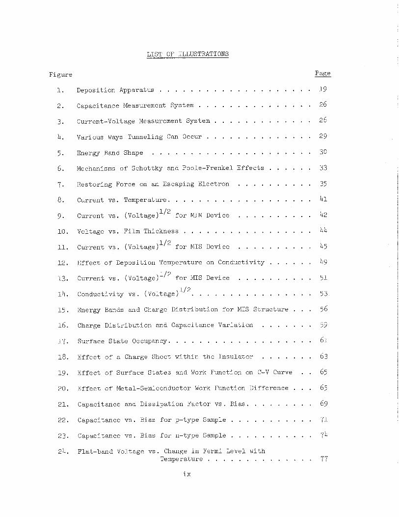
LIST OF ILLUSTRATIONS
Figure Page
. . . . . . . . . . . . . . . . . . . . Deposition Apparatus 19
. . . . . . . . . . . . . . . Capacitance Measurement System 26
. . . . . . . . . . . . . Current-Voltage Measurement System 26
. . . . . . . . . . . . . . Various Ways Tunneling Can Occur 29
. . . . . . . . . . . . . . . . . . . . . Energy Band Shape 30
. . . . . . Mechanisms of Schottky and Poole-Frenkel E f f e c t s 33
. . . . . . . . . . Restoring Force on an Escaping Elec t ron 35
. . . . . . . . . . . . . . . . Current vs . Temperature
Current vs . f o r M I M Device . . . . . . . . . . . . . . . . . . . . . Voltage vs . Film Thickness
. . . . . . . Current vs . (Voltage)'l2 f o r MIS Device
Ef fec t of Deposition Temperature on Conductivity . . . Current vs . f o r MIS Device . . . . . . .
112 . . . . . . . . . . . . . . Conductivity vs ( v o l t a g e )
Energy Bands and Charge D i s t r i b u t i o n f o r MIS S t r u c t u r e
Charge D i s t r i b u t i o n and Capacitance Var ia t ion . . . . . . . . . . . . . . . . . . . . . . . Surface S t a t e Occupancy 61
Ef fec t of a Charge Sheet w i th in t h e I n s u l a t o r . . . . . . . 63 Ef fec t of Surface S t a t e s and Work Function on C-V Curve . . 65
E f f e c t of Metal-Semiconductor Work Function Difference . . . 65
. . . . . . . . . Capacitance and Di s s ipa t ion Fac tor vs . Bias 69
. . . . . . . . . . . . Capacitance vs Bias f o r p-type Sample 71
. . . . . . . . . . . Capacitance vs . Bias f o r n-type Sample 74
Flat-band Voltage vs . Change i n Fermi Level with . . . . . . . . . . . . . . Temperature 77
Figure Page
. . . . . . . . . . . . 25 . Equivalent C i r c u i t of MIS Capaci tor 80
. . . . . . . 26 . Capacitance vs . Bias f o r "PB" Prepared Samples 84
. . . . . . . . . 27 . Elec t rode E f f e c t s on Capacitance vs . Bias 86
. . . . . . . . . . . . 28 . SiO E f f e c t s on Capacitance vs . Bias 87 2
LIST OF SYMBOLS
Area (cm)
Tota l Capacitance ( f a r a d s )
Oxide capaci tance ( f a r a d s )
Space charge capac i tance ( f a r ads )
Capacitance of space charge l a y e r a t f l a t band ( f a r a d s )
Flat-band capac i tance ( f a r a d s )
Surface s t a t e capac i tance ( f a r a d s )
Equivalent p a r a l l e l capac i tance ( f a r ads )
Measured capac i tance ( f a r a d s )
Film th i ckness (cm)
Charge on an e l e c t r o n = 1 . 6 x 10-l9 (coulombs )
Fermi energy (eV)
h e s t energy i n conduction band (eV)
Highest energy i n valence band (eV)
Energy of donor s i t e s ( e ~ )
Energy of acceptor s i t e s ( e ~ )
Free energy ( k i l o - c a l )
Measured conductance (mhos )
Surface conductance (mhos)
Equivalent p a r a l l e l conductance (mhos )
Randit s cons tan t = 6.62 x ( jou le - sec )
Heat content of t h e system a t cons tan t p re s su re ( k i l o - c a l )
Current ( amps )
2 Current dens i ty ( amps/cm )
Boltzmann's cons tan t = 1 . 3 8 x ( j o u l e / O ~ )
Debye l eng th (cm)
Slope of t h e Schottky type p l o t (mlvo l t ) 1 / 2
E f f e c t i v e mass ( k g )
Acceptor concent ra t ion ( cmW3)
Donor con cen t r a t ion (
E f f e c t i v e dens i ty of s t a t e s i n conduction band (cm-')
E f f e c t i v e dens i ty of s t a t e s i n valence band ( ~ m - ~ )
Concentration of f r e e c a r r i e r s (cm-')
I n t r i n s i c c a r r i e r concent ra t ion (em-')
Density of s t t e s i n conduction band, inc luding concent ra t ion of t r a p s (cm-'1
2 Oxide space charge dens i ty ( s t a t e s l c m )
2 I n t e r f a c e s ta , te charge dens i ty (s tates/ev-cm )
Charge on t h e c a r r i e r s (coulomb)
2 Oxide space charge (coulombs/cm )
;i: I n t e r f a c e s t a t e charge (coulombs/cm )
2 Surface s t a t e dens i ty (coulombs/cm )
Parameter ranging between 1 and 2 depending on degree of compensa- t i o n
Entropy ( cal/degree-mole )
Tempera,ture (OK)
Elec t ron hole p a i r genera t ion r a t e ( c a r r i e r s l s e c )
Bulk p o t e n t i a l ( v o l t s )
Surface p o t e n t i a l ( v o l t s )
Flat-band vol tage ( v o l t s )
Voltage ( v o l t s )
Deplet ion l a y e r width i n semiconductor (cm)
Space charge width i n i n s u l a t o r (cm)

A 'PF
*'s
'ms
'm
's
'0
'max
'
t a n 6
High frequency d i e l e c t r i c cons tan t of d i e l e c t r i c
12 P e r m i t t i v i t y of f r e e space = 8.85 x 10 (farads/m)
E l e c t r i c f i e l d (vol t s /cm)
Act iva t ion energy (eV)
Low frequency d i e l e c t r i c constant of d i e l e c t r i c
D i e l e c t r i c cons tan t of semiconductor
Wavelength (em)
B a r r i e r lowering f o r Poole-Frenkel emission ( e v )
B a r r i e r lowering f o r Schottky emission ( e v )
Metal-semiconductor work func t ion ( v o l t s )
Metal work func t ion ( v o l t s )
Semi conductor work func t ion ( v o l t s )
P o t e n t i a l b a r r i e r a t t h e i n t e r f a c e (eV)
Maximum b a r r i e r a t t h e i n t e r f a c e (eV)
Energy d i f f e rence between emission s i t e and bottom of conduction band ( e v )
Metal p o t e n t i a l b a r r i e r ( e ~ )
Semiconductor p o t e n t i a l b a r r i e r ( e v )
I n s u l a t o r p o t e n t i a l b a r r i e r (eV)
Charge dens i ty ( coulomb/ em3)
Conductivity (mhos /em)
Diss ipa t ion f a c t o r
2 Mobil i ty of c a r r i e r s (cm /vo l t - s ec )
+ - EF ( e v )
Frequency = 2nf ( r a d i a n s / s e c )
Majori ty c a r r i e r t ime cons tan t ( s e c )
E f fec t ive c a r r i e r l i f e t i m e i n dep le t ion reg ion ( s e c )
CHAPTER I.
INTRODUCTION
Present e f f o r t s on d i e l e c t r i c t h i n f i lms emphasize t h e i r formation
by ox ida t ion , anodizat ion , evapora t ion , and s p u t t e r i n g . Chemical vapor dep-
o s i t i o n o f f e r s s e v e r a l advantages over o t h e r methods o f d i e l e c t r i c f i l m
growth, such a s v e r s a t i l i t y i n choice of s u b s t r a t e , homogenous oxide f i l m ,
a sha rpe r and c l eane r i n t e r f a c e , g r e a t e r c o n t r o l over t h e composition o f t h e
film, and more c o n t r o l over t h e th i ckness and growth r a t e .
To be compatible with i n t e g r a t e d c i r c u i t s , a t h i n f i l m c a p a c i t o r
must s a t i s f y s e v e r a l c r i t e r i a , i nc lud ing low d i s s i p a t i o n f a c t o r , high s t a -
b i l i t y during i n t e g r a t e d c i r c u i t p rocess ing , vo l tage i n s e n s i t i v i t y , and high
y i e l d . Many ma te r i a l s c u r r e n t l y used a s capac i to r d i e l e c t r i c s f o r t h i n f i l m
m i c r o c i r c u i t s e x h i b i t low d i e l e c t r i c cons t an t s o r low breakdown vol tage . Ti-
tanium dioxide i s a t t r a c t i v e a s a d i e l e c t r i c m a t e r i a l i n i n t e g r a t e d c i r c u i t s
1 9 s i n c e t h e d i e l e c t r i c cons tan t i n r u t i l e p a r a l l e l t o t h e C-axis i s 170
High d i e l e c t r i c constant m a t e r i a l s o f f e r t h e advantage of h ighe r capac i tance
without t h e neces s i ty f o r l a r g e r a r eas o r t h i n n e r f i lms which l e a d t o p i n
ho le s and device f a i l u r e . I n t h e p re sen t work organometa l l ics of t i t a n i u m i n an ox id i z ing a t -
mosphere conta in ing water vapor from hydrogen and carbon dioxide form t h i n
f i lms of t i t a n i u m dioxide wi th d e s i r a b l e d i e l e c t r i c p r o p e r t i e s on meta ls and
on s i l i c o n ,
A, Other Work on Titanium Dioxide.
Titanium dioxide f i lms f o r o p t i c a l app l i ca t ions were f i r s t prepared
6 3 by oxida t ion of t h e metal i n air and anodiza t ion of t h e meta l Titanium
7 4 dioxide f i l m s f o r d i e l e c t r i c a p p l i c a t i o n s have been prepared by anodiza t ion ,
chemical vapor depos i t ion of t i t a n i u m t e t r a c h l o r i d e and t e t r a i s o p r o p y l
t i t a n a t e wi th water vapor ( s team) at a s u b s t r a t e temperature of 150°C 49,50 Y
chemical vapor depos i t i on of t e t r a i s o p r o p y l t i t a n a t e i n an oxygen atmosphere
89 81 a t 700°C138, glow d i scha rge , r e a c t i v e s p u t t e r i n g , and by d i r e c t evaporat ion
65 of t i t an ium dioxide by hea t ing i n a vacuum . MartinB9, i n 1962, r epo r t ed t h e formation o f Ti0 f i lms by glow
2
discharge. Leaking r e a c t i v e gases i n t o an evacuated b e l l j a r i n t h e v ic in-
i t y of t h e discharge forms t h e f i lms . The f i l m s were amorphous with a di-
e l e c t r i c cons tan t of 90 , bu t became c r y s t a l l i n e wi th a d i e l e c t r i c constant
0
of 40 when h e a t t r e a t e d a t 350°C f o r one-half hour. For 2500 A f i lms a t 1
kHz t h e capac i tance p e r u n i t was . 1 5 p ~ / c m ~ , with a d i s s i p a t i o n f a c t o r of 2.6%
and a breakdown s t r e n g t h of 4 x l o 5 volts/cm.
LakshmananB1, i n 1963-65, used r e a c t i v e s p u t t e r i n g t o form f i lms of
t i t an ium oxide. Pure t i t a n i u m cathodes i n an oxygen-argon gas mixture forms
2 t he f i lms . Capacitance of .30pF/cm and d i s s i p a t i o n f a c t o r s of 5.5% a t 1 kHz
0
a r e r epo r t ed f o r f i lms between 1000 and 1600 A t h i c k .
Von ~ i ~ ~ e 1 ~ ~ ~ , i n 1964, r epo r t ed on t h e growth and s t r u c t u r e of ti-
tanium f i lms on a l k a l i h a l i d e c r y s t a l s and t h e e f f e c t of c o n t r o l l e d ox ida t ion
of t h e s e f i lms while van ~ a a l t z i f t h e same l a b o r a t o r y , r epo r t ed on conduc-
t i o n phenomena i n r u t i l e s i n g l e c r y s t a l s . He r epor t ed an inc reas ing conduc-
t i v i t y wi th t ime due t o i nc reased e f f e c t i v e c a r r i e r mob i l i t y caused by t h e
f i l l i n g of shallow t r a p s and due t o an inc reased p o s i t i v e space charge
throughout t h e bulk o f t h e c r y s t a l , enhancing e l e c t r o n i n j e c t i o n .
I n t h e 1963-64 Feuersanger 49 y 5 0 formed t h i n f i l m s of Ti0 by t h e 2
vapor r e a c t i o n of t i t a n i u m t e t r a c h l o r i d e o r t e t r a i s o p r o p y l t i t a n a t e w i th
water vapor a t a s u b s t r a t e temperature of 150°C. The wa te r vapor i s i n t r o -
duced i n t h e form of steam from oxygen o r n i t rogen bubbled through hot wa te r ,
Z These f i lms have d i e l e c t r i c cons t an t s of 80 and capac i tances of 0.5pF/cm

5 .
with a d i s s i p a t i o n f a c t o r of 2.3% and a breakdown s t r eng th of 2-7 x 10 5
v o l t s /em.
138 Very r ecen t ly Yokozawa formed t h i n f i lms of t i t an ium dioxide by
t h e decomposition of t e t r a i s o p r o p y l t i t a n a t e i n a dry oxygen atmosphere a t
700°C. The f i lms were porous and e a s i l y etched by d i l u t e d HF. The f i lms
cons i s t of f i n e c r y s t a l l i t e s of anatase . The r e f r a c t i v e index i s 2.0. No
e l e c t r i c a l da ta i s repor ted f o r these f i lms .
1n 1965 peterson '03"04 deposi ted t i t an ium dioxide f i lms by t h e
r eac t ion of t e t r a i s o p r o p y l t i t a n a t e with oxygen a t a s u b s t r a t e temperature
of from 300-500°C. However, he discontinued t h i s work because of low die lec-
5 t r i c s t r e n g t h ( 3 x 10 volts /cm) and i n s t a b i l i t y of t h e f i l m t o e l e c t r i c a l
s t r e s s . The anodized f i lms of Ti02 form only on t i t an ium s u b s t r a t e s and
show a d i e l e c t r i c constant of about 40. Direct evaporat ion of t i t an ium di-
oxide by hea t ing i n a vacuum r e s u l t s i n a l o s s of oxygen of t h e evaporant.
Such depos i t s a re semiconducting r a t h e r than i n s u l a t i n g .
The above authors r e p o r t only a l i m i t e d amount of e l e c t r i c a l da ta ,
iYO Maserjian and Mea descr ibe t h e e l e c t r i c a l p rope r t i e s of t h i n f i l m
sandwiches of A1-Ti0 -A1 with evaporated f i lms varying i n th ickness from 100 2
0
t o 410 A. Their r e s u l t s a re i n t e r p r e t e d i n terms of a l a r g e i o n i c space
charge i n t h e Ti02 f i lms . These f i lms have a d i e l e c t r i c constant of 27.
B. S igni f icance of t h i s Work.
A knowledge of t h e conduction behavior of t i t an ium dioxide f i lms on
s i l i c o n and metal coated qua r t z s u b s t r a t e s with d i f f e r e n t contac ts i s t he
expected r e s u l t of t h i s work. The exis tence of a l a r g e i o n i c space charge
as observed by ~ a s e r j i a n " f o r very t h i n evaporated f i lms would not neces-
s a r i l y be expected f o r these t h i c k e r films formed by CVD due t o t h e d i f f e r -
ence i n processing. This type of da ta and t h e s e r e s u l t s have been unex-
67 p lo red p r i o r t o t h i s work .

4.
The capaci tance-vol tage d a t a y i e l d information about t h e o u t e r oxide
su r f ace s t a t e d e n s i t y , t h e f a s t i n t e r f a c e su r f ace s t a t e d e n s i t y , frequency
e f f e c t s due t o t h e va r ious source m a t e r i a l s , e l ec t rode e f f e c t s , and SiO - 2 67 Ti0 mixture e f f e c t s t h a t have not been r epor t ed by o the r i n v e s t i g a t o r s a
2
The experimental technique resembles t h a t of ~ e u e r s a n g e r ~ ~ and
~ o k o z a w a l ~ ~ , bu t i s d i f f e r e n t i n t h a t hydrogen and carbon dioxide form
t h e water vapor i n p re fe rence t o bubbling t h e c a r r i e r gas through heated
waterS0 o r dry 0 138s Feuersanger 'sSO technique has t h e advantage of low 2
depos i t ion temperature (150°C versus 900°C), however, t h e hydrogen and car-
bon dioxide seems t o be more d e s i r a b l e f o r reasons enumerated i n Chapter 111.
C. Experimental Techniques -
The main experimental technique app l i cab le t o t h i n f i l m d i e l e c t r i c s
i s a s tudy of t h e i r e l e c t r i c a l p r o p e r t i e s . The experimental program involves
making metal-insulator-met a1 (MIM) s t r u c t u r e s and metal-insulator-semiconduc-
t o r (MIS) s t r u c t u r e s and measuring t h e i r capaci tance and conduction.
Two b a s i c techniques apply t o t h e s tudy of t h e e l e c t r i c a l proper-
t i e s : Capacitance versus b i a s versus frequency and dc cu r r en t t r a n s p o r t .
Capacitance d a t a g ive information about t h e i n t e r f a c e s t a t e s , oxide su r f ace
s t a t e s , and d i e l e c t r i c cons t an t s . The cur ren t -vol tage measurements a t var-
i ous temperatures y i e l d informat ion about t h e breakdown s t r e n g t h of t h e ma-
t e r i a l , uniformity of t h e f i l m s , var ious conduction mechanisms, b a r r i e r
h e i g h t s , and t r a p l e v e l s i n t h e energy band.
A knowledge o f cur ren t -vol tage c h a r a c t e r i s t i c s he lps t he device en-
g i n e e r , a s w e l l a s supplying b a s i c information about t h e m a t e r i a l . These
3 3 c h a r a c t e r i s t i c s r e l a t e t o t h e design of f i e l d e f f e c t t r a n s i s t o r s (FET) a
The leakage cu r ren t o f t h e d i e l e c t r i c a f f e c t s t h e c h a r a c t e r i s t i c s and must
be considered i n des ign , This leakage cu r ren t a l s o provides warning as t h e
5 .
d i e l e c t r i c approaches breakdown. This current-voltage behavior i s a l s o of
importance t o t h e design of new surface s t a t e and i n t e r f a c e d i g i t a l t r ans -
72 ducer concepts described by Hartwig . Surface-state d e n s i t i e s gained from capacitance-voltage d a t a i s
a l s o of importance t o device engineers . More f a s t su r face s t a t e s can de-
c rease t h e channel mobi l i ty causing lower gain-bandwidth products i n
MOSFET's. They a l s o inc rease t h e switching v ~ l t a g e of enhancement mode
FET's. Fas t sur face s t a t e s a f f e c t MOS performance by a l t e r i n g t h e reac-
tance of t h e MOS varac tors by f i l l i n g and emptying of charge i n and out of
these s t a t e s a t t h e ac measurement frequency. Also, t h e charge i n t h e
s t a t e s i s an added component t o t h e su r face charge a t t h e insulator-semicon-
ductor i n t e r f a c e . Oxide su r face - s t a t e dens i ty i s a parameter which con t ro l s
t h e threshold of MOS enhancement mode FET swi tches , t h e opera t ing po in t of
MOS deple t ion mode FET a m p l i f i e r s , t h e PNP t r a n s i s t o r c o l l e c t o r junct ion
3 3 leakage , and p a r a s i t i c su r face capaci tance .
CHAPTER 11
FILM FORMATION TECHNIQUES
Seve ra l techniques e x i s t f o r forming d i e l e c t r i c t h i n f i lms , A l l t h e
d i e l e c t r i c f i l m formation techniques have both advantages and disadvantages,
Surface r e a c t i o n s l i k e oxida t ion depend on an appropr i a t e s t a r t i n g m a t e r i a l ,
bu t process e a s i l y , Vacuum evaporat ion r e a d i l y forms f i lms of m a t e r i a l s
which vaporize congruent ly a t "reasonable" tempera tures , b u t most d i e l e c t r i c s
do not evaporate congruent ly. F lash evaporat ion avoids atomic spec i e s sepa-
r a t i o n , bu t r e q u i r e s s p e c i a l apparatus and a s o l i d powder form of source ma-
t e r i a l .
The m u l t i p l e forms of s p u t t e r i n g made it a wide ranging technique .
DC s p u t t e r i n g works f o r m e t a l l i c anode m a t e r i a l s . RF o r AC s p u t t e r i n g can
avoid space charge build-up on i n s u l a t i n g source m a t e r i a l s by n e u t r a l i z a t i o n
from t h e plasma e l e c t r o n s . The g r e a t e s t v e r s a t i l i t y of s p u t t e r i n g a r i s e s
through chemical r e a c t i o n at t h e source , i n t h e g a s , o r a t t he t a r g e t i n t h e
process of r e a c t i v e s p u t t e r i n g . Mul t ip le -e lec t rode s p u t t e r i n g o f f e r s another
way t o form f i lms conta in ing s e v e r a l atomic s p e c i e s , bu t r equ i r e s f a i r l y com-
p l e x process ing .
Chemical vapor depos i t ion uses a b a s i c a l l y simple r eac t$ on chamber
f o r any k ind of r e a c t i o n . The process complicat~ions a r i s e i n obta in ing gas-
eous r e a c t a n t s , c o n t r o l l i n g t h e flow of r e a c t a n t s and c a r r i e r gases , and op-
t imiz ing t h e flow of gases around t h e s u b s t r a t e . I n p r i n c i p l e , however, nea r ly
any m a t e r i a l can be formed on nea r ly any o t h e r m a t e r i a l t h a t i s thermal ly and
chemically compatible.
The d e t a i l e d c h a r a c t e r i s t i c s of d i e l e c t r i c f i lms may depend s i g n i f i -
can t ly on t h e formation p roces s . This s e c t i o n d i scusses t h e s e processes i n
g r e a t e r de ta i 1.
7 A. Sput ter ing .
Sputter ing i s a process whereby t h e impact of a s tream of acce ler -
a t e d ions vaporizes a t a r g e t . I n dc s p u t t e r i n g , s e v e r a l thousand v o l t s dc
a re placed between two e lec t rodes i n a vacuum of t o 10-1 t o r r . The re-
s u l t i n g glow discharge contains high energy i o n s , acce le ra t ed by t h e high
f i e l d , which s t r i k e t h e cathode and dislodge n e u t r a l atoms o r molecules.
These n u e t r a l spec ies r a d i a t e outwards from t h e t a r g e t su r face and depos i t
on a subs t ra te45. This technique r equ i re s t h e t a r g e t t o be a conductor as
otherwise t h e i n i t i a l bombarding ions c r e a t e a region of p o s i t i v e space
charge i n t h e v i c i n i t y of t h e t a r g e t thereby sh ie ld ing t h e t a r g e t from fur-
t h e r bombardment. RF s p u t t e r i n g techniques avoid t h i s by applying an RF
vol tage t o t h e t a r g e t with respect t o t h e plasma. On a l t e r n a t e h a l f cyc les ,
t h e p o s i t i v e space charge bu i ld ing up i s neu t ra l i zed by plasma e l e c t r o n s . RF
s p u t t e r i n g i s a u s e f u l technique f o r t h e deposi t ion of in su la to r s42 with the
l i m i t a t i o n t h a t t h e atomic species i n t h e f i l m deposi ted i s t h e same as t h a t
of t h e t a r g e t . In r e a c t i v e s p u t t e r i n g , some chemical r eac t ion takes place
p r i o r t o spu t t e r ing ( t h e su r face of the t a r g e t i s a l t e r e d t o possess a t h i n
r eac ted surface l a y e r ) , during s p u t t e r i n g ( t h e species dislodged during bom-
bardment i s reac ted chemically during i t s t r anspor t t o t h e s u b s t r a t e su r face ) 121
o r a f t e r s ,put ter ing ( t h e f i l m deposi ted on t h e s u b s t r a t e su r face i s a l t e r e d
through some chemical r e a c t i o n ) .
Non-reactive s p u t t e r i n g i s s u i t a b l e f o r t h e deposi t ion of metals and
conductors while r e a c t i v e s p u t t e r i n g i s s u i t a b l e f o r t h e deposi t ion of die-
l e c t r i c s . The requirement of maintaining a gas discharge l i m i t s t h e p r a c t i -
c a l range of gas pressure and inf luences the use fu l range of gas mixtures.
Advantages of s p u t t e r i n g include t h e f a c t t h a t t h e s u b s t r a t e tempera-
t u r e can be lower than i n CVD. This allows t h e f i lms t o be deposi ted on sub-
s t r a t e s which would melt a t high temperatures (i. e , , ~ 1 ) .
8.
The c leaning of su r f aces t o be coated by phys i ca l vapor depos i t i on
6 methods i s more d i f f i c u l t than t h a t r equ i r ed f o r CVD . No vigorous chemical
ac t ion occurs at t h e su r f ace a s an inhe ren t p a r t of t h e coa t ing process a s i n
CVD. Spu t t e r ing does produce more adherent f i lms than vacuum evaporat ion be-
cause of t h e g r e a t e r i on ene rg i e s , The s u b s t r a t e temperature i s normally suf -
f i c i e n t l y low during depos i t ion t h a t l i t t l e d i f f u s i o n of t h e depos i t i n t o t h e
s u b s t r a t e occurs .
B, Vacuum Evaporation.
Vacuum evapora t ion i s b a s i c a l l y simple i n theory and i n many appl ica-
t i o n ~ ~ ~ . The m a t e r i a l t o be app l i ed i s hea ted i n a high vacuum t o a tempera-
t u r e a t which i t s vapor p re s su re i s about t o r r o r g r e a t e r . Thus, t h i s
process involves t h e t r a n s f e r of m a t e r i a l and t h e formation of coa t ings by
phys ica l means a lone . I n t h e evaporat ion of non-elemental m a t e r i a l ( i . e . , compounds ) , d i s s o c i a t i o n o r incongruent evaporat ion may occur , followed by
6 varying degrees of recombination of t h e compounds a t t h e p l ace of impingement . Since no chemical r e a c t i o n occurs a t t h e su r f ace a s an inhe ren t p a r t o f t h i s
p roces s , t h e c leaning of su r f aces i s d i f f i c u l t . wi th t h i s technique ,
One obvious advantage t o t h i s technique i s t h e low s u b s t r a t e tempera-
t u r e r equ i r ed . Other vacuum methods a r e a v a i l a b l e f o r t h e depos i t ion of com-
pounds, One of t h e s e i s f l a s h evapora t ion . Films of BaTiO and SrTiO have 3 3
been prepared 9 7 3 9 8 by t h i s method. Ind iv idua l g ra ins of t h e compound a r e fed
onto a hot su r f ace a t a r a t e such t h a t one v o l a t i l i z e s completely before t h e
next one a r r i v e s . This method does not o f f e r much d e s i r a b l e v a r i a t i o n i n t h e
composition of t h e depos i ted f i lm . The depos i t i on of compounds by co-deposi-
t i o n from mul t ip l e vapor sources r equ i r e s accu ra t e knowledge and c o n t r o l of
vapor source tempera ture , a r e a s , and vapor i za t ion r a t e s Because of t h e d i f f i -
c u l t i e s involved i n secur ing and maintaining t h e s e cond i t i ons , t h i s technique

6 has n o t been used t o any g r e a t ex t en t . C . Thermal. Deposition.
35 Thermal oxida t ion i s an important technique f o r forming t h i n f i lms . S i l i c o n dioxide thermal ly grown on s i l i c o n i s t h e b e s t example of t h i s tech-
nique. Thermal ox ida t ion disadvantages inc lude f i l m not s t r u c t u r a l l y p e r f e c t ,
f i l m p u r i t y not p e r f e c t , high temperature r equ i r ed , abnormal t r a n s i t i o n re -
gions a t meta l - insu la tor o r semiconductor- insulator i n t e r f a c e , and t h e compo-
s i t i o n of t h e f i l m i s l i m i t e d by t h e s u b s t r a t e . The main ob jec t ions r e a l l y
stem from t h e f a c t t h a t y e a r s of t echno log ica l development have y e t t o make
t h e s e ma te r i a l s perform as s a t i s f a c t o r i l y as device r e l i a b i l i t y and perform-
ance c r i t e r i a demand.
D. Chemical Vapor Deposi t ion.
I n CVD s o l i d depos i t s a r e formed by chemical r e a c t i o n s which t a k e
p l ace on, a t , o r nea r t h e depos i t i on su r f ace . Vapor depos i ted m a t e r i a l s a r e
of g r e a t importance a t p r e s e n t and promise even g r e a t e r importance because
t h e depos i t ion process i s an extremely v e r s a t i l e and u s e f u l l y inexpensive
6 method of molecular forming . While i n phys i ca l vapor depos i t ion t h e medium
i s a vacuum o r a r a r e f i e d g a s , i n CVD t h e medium i s a chemically r e a c t i v e gas
mixture which i s thermal ly a c t i v a t e d t o depos i t m a t e r i a l . CVD has t h e d i s -
advantage t h a t t h e s u b s t r a t e must be hea ted t o r e l a t i v e l y high tempera tures ,
b u t t h e s e temperatures would not be de t r imen ta l i n many a p p l i c a t i o n s . It has
6 t h e advantage t h a t it i s app l i cab le t o t h e wides t range of m a t e r i a l s .
I n CVD and i n phys i ca l vapor depos i t ion f eed vapors a r e genera ted by
evaporat ion from a su r f ace and t h e v o l a t i l i z e d m a t e r i a l i s t hen t r a n s p o r t e d
t o a s u b s t r a t e on which it condenses o r decomposes.
With CVD it i s p o s s i b l e t o v o l a t i l i z e s e l e c t i v e l y a feed m a t e r i a l ,
t r a n s p o r t it t o t h e d e s i r e d l o c a t i o n , and p r e c i p i t a t e it as a c o n t r o l l e d

s t r u c t u r e . Fu r the r p u r i f i c a t i o n can be achieved i n t h e chemical t r a n s p o r t
system by s e p a r a t e d i s t i l l a t i o n of t h e v o l a t i l e i n t e rmed ia t e s , as w e l l a s
s e l e c t i v e r e a c t i o n e i t h e r a t t h e source o r a t t h e hea ted s u b s t r a t e .
By reason of t h e very l a r g e number of a v a i l a b l e chemical r e a c t i o n s ,
b CVD i s seen t o be a process of g r e a t v e r s a t i l i t y and f l e x i b i l i t y . It does
not r e q u i r e t h e use of i on izab le compounds o r any degree of e l e c t r i c a l con-
d u c t i v i t y i n t h e s u b s t r a t e o r depos i t . Highly i n s u l a t i n g ma te r i a l s a r e de-
p o d e d a s r e a d i l y as pure me ta l s , Also, CVD can be used t o depos i t compounds
which a r e t o o uns t ab le t o be depos i ted without marked change i n composition
by p h y s i c a l vapor depos i t i on , CVD can be c a r r i e d out over a pressure range
from super-atmospheric down t o pressures c h a r a c t e r i s t i c of phys i ca l vapor
depos i t ion ,
~ l o c h e r ' l ~ r e c e n t l y enumerated t h r e e main d i f f e r ences i n CVD and sim-
p l e condensation. (1) Simple condensation i s exothermic and most u s e f u l CVD
r eac t ions a r e endothermic. By the use of endothermic processes , t h e reac-
t i o n s can be delayed more e f f e c t i v e l y u n t i l t h e r e a c t a n t gases reach t h e
hea ted s u b s t r a t e . The use of endothermic r eac t ions gene ra l ly in t roduces an
apprec iab le energy b a r r i e r t o t h e k i n e t i c s of t h e r e a c t i o n , bu t a t t h e h ighe r
pressures and temperatures of CVD equi l ibr ium i s more e a s i l y approached than
i n simple condensat ion, (2) Though vacuum evaporation-condensation p l a t i n g
processes ope ra t e a t p re s su re s i n t h e molecular flow reg ion , CVD ope ra t e s i n
t h e viscous flow region wit,h a s soc i a t ed c a r r i e r gases through which t h e re-
a c t a n t must d i f f u s e t o reach t h e s u b s t r a t e . Carl ton and 0xley112 thoroughly
d iscuss t h i s s u b j e c t . This d i f f u s i o n b a r r i e r p l aces an upper l i m i t on t h e
a t t a i n a b l e nuc lea t ion dens i ty , However, t h e r a t i o of t h e nuc lea t ion r a t e t o
growth r a t e depends on t h e na tu re of t h e system and t h e temperature and can
be v a r i e d t o i nc rease nuc lea t ion , ( 3 ) Whereas only t h e condensable vapor of

t h e m a t e r i a l be ing depos i ted need be considered i n a c lean condensation sys-
tem, CVD involves o t h e r chemical spec i e s . These i n t r i n s i c i m p u r i t i e s a r e con-
s i d e r e d t o have a number of p o s s i b l e e f f e c t s depending on t h e na tu re o f t h e
impur i ty , t h e adsorbed monomer and t h e s u b s t r a t e . Since such e f f e c t s would
be s p e c i f i c t o t h e system i n ques t ion and would ope ra t e i n many d i r e c t i o n s ,
it i s impossible t o account f o r them q u a n t i t a t i v e l y .
'Ihe e x p i t a x i a l growth o f e lemental semiconductors by chemical vapor
depos i t i on i s now a w e l l e s t a b l i s h e d technique 2,35,36,79,114,128 , i n s p i t e
of i t s s l o 5 ~ i n i t i a l acceptance. Two major vapor phase systems used f o r t h e
elemental semiconductor grcwth a r e p y r o l y t i c decomposition of h a l i d e s o r hy-
d r i d e s and t h e hydrogen r educ t ion of h a l i d e s .
The product ion of pigments and r e i n f o r c i n g agents i s t h e l a r g e s t ap-
6 p l i c a t i o n of CVD t o d a t e . Carbon blacks and pigment-grade t i t an iuni dloxide
made by burning TiC14 a r e t h e l a r g e s t i tems of importance. Next i n import-
ance a r e t h e carbonyl m e t a l s , p a r t i c u l a r l y n i c k e l .
The need. f o r r e f r a c t o r y m a t e r i a l s i n t h e aerospace i n d u s t r y i s an
important a p p l i c a t i o n o f CVD. Niobium, molybdenum, tan ta lum, and tungs ten
a r e convenient ly depos i ted by hydrogen reduct ion of t h e corresponding h a l i d e
vapors , Refractory meta l carb ides a r e obta ined by r e a c t i o n of t h e meta l ha l -
i d e s wi th hydrocarbons.
6 Many metals have been succes s fu l ly depos i ted by CVD. Powell g ives
summaries of t h e condi t ions used t o prepare depos i t s of Al, As, Sb, B i , C r ,
Co, Cu, Ge, Au, Fe , Pb, Mo, N i , Ta, P t , Re, Sn, T i , W , U , V , and Z r , Numer-
6 ous re ferences a r e given f o r each metal . Powell a l s o g ives a s i m i l a r t r e a t -
ment f o r chemically depos i ted nonmetals such a s boron and bo r ides 55,57 , car-
bon and ca rb ides , n i t r i d e s , s i l i c o n and s i l i c i d e s , and oxides. O f g r e a t i m -
por tance i n t h e mic roe l ec t ron ic s f i e l d i s t he r ecen t work i n CVD of S i c 30,76 Y
6 S i N 29 y 4 0 y121y136 and s ~ o ~ ~ y91. Powell l i s t s re ferences f o r CVD o f var- 3 4
i ous oxides , inc luding A 1 0 Cr203, GeO, Fe 0 SiO Ti0 and o t h e r s . 2 3 ' 2 3 , 2 ' 2 y
Chemical vapor depos i t i on o f f e r s s e v e r a l advantages over o t h e r meth-
ods. Some of t h e s e advantages a r e :
1. Much v e r s a t i l i t y i s p o s s i b l e s i n c e f i lms can be depos i ted on
me ta l s , semiconductors, o r o t h e r d i e l e c t r i c s .
2. The oxide f i l m should be very homogeneous s i n c e t h e r e a c t a n t
emanates from a source wi th preservable i n t e g r i t y .
3. The composition of t h e f i l m can be c o n t r o l l e d independent ly of
t h e composition of t he s u b s t r a t e .
4, The processes involved gene ra l ly can be c a r r i e d out a t lower
temperatures than t h o s e r equ i r ed f o r depos i t ion i n i no rgan ic
systems,
5 . The r e a c t a n t and product vapors of t h e organic systems a r e
u sua l ly l e s s r e a c t i v e and co r ros ive than those of t h e ino rgan ic
systems,
6, Coating th i ckness can be v a r i e d , and f a i r l y w e l l c o n t r o l l e d over
a wide range.
7. The very l a r g e number of a v a i l a b l e chemical r e a c t i o n s a s su re s
chemical vapor depos i t i on t o be a process of g r e a t v e r s a t i l i t y
and f l e x i b i l i t y .
8, The organic r e a c t i o n s a r e more s u i t a b l e f o r t h e p repa ra t ion of
h igh p u r i t y oxides .
9 . Due t o t h e l a r g e number of v a r i a b l e s , such as gas tempera ture ,
gas flow r a t e , s u b s t r a t e temperature and t ime , g r e a t e r con t ro l
over f i l m composition i s p o s s i b l e .
CHAPTER I11
FUNDAMENTALS OF CVD
A. Vapor P l a t i n g Requirements.
The gene ra l requirements f o r any gas p l a t i n g r e a c t i o n may be sum-
marized a s fol lows :
1, The r e a c t a n t s must be i n t h e gaseous o r vapor s t a t e ;
2 t h e product t o be deposi ted must be condensible a t t h e sub-
s t r a t e ; and
3. t h e by-products formed i n t h e r e a c t i o n chamber must be suf -
f i c i e n t l y v o l a t i l e t o allow t h e i r ready removal.
I n add i t i on t o t hese genera l requirements , t h e thermodynamics and
k i n e t i c s of any p a r t i c u l a r vapor p l a t i n g r e a c t i o n s impose r e s t r a i n t s upon
t h e depos i t ion temperature and r e a c t a n t concent ra t ions which a r e unique t o
6 t h e r eac t ion under cons idera t ion . B. Basic K ine t i c Considerat ions.
6 A number of s t e p s must occur f o r t h e o v e r a l l depos i t ion : Diffus ion
of t h e r eac t an t through t h e s t a t i c l a y e r ad jacent t o t h e s u b s t r a t e ; adsorp-
t . ion onto t h e s u b s t r a t e ; d i f f u s i o n of t h e adsorbed spec i e s across t h e sur-
face t o a c t i v e s i t e s ; t h e chemical r e a c t i o n ; depos i t ion of t h e non-vola t i le
products ; desorp t ion of t h e v o l a t i l e products ; and t h e i r d i f f u s i o n away from
t h e v i c i n i t y of t h e s u b s t r a t e , The f i r s t and l a s t s t e p s a r e gene ra l ly no t
independent, s i n c e t h e d i f f u s i o n r a t e of t h e r e a c t a n t s a f f e c t s t h e d i f f u s i o n
r a t e of t h e products , and s to ich iometry in f luences t h e two s t e p s of t h e re -
a c t i o n , and both a f f e c t t h e chemical r e a c t i o n r a t e . The complex in t e rmed ia t e
s t e p s normally involve su r f ace and gaseous rea,ctions , as w e l l a s simultaneous
adsorpt ion-desorpt ion and nuc lea t ion processes . Any of t h e above s t e p s may
determine t h e r a t e of depos i t i on . Each s t e p has a temperature dependence
1 3
which determines i t s r e l a t i v e importance. I n t h e low-temperature range
( < 3 5 0 ' ~ ) t h e depos i t ion r a t e depends predominately on t h e chemical k i n e t i c s .
That i s , t h e depos i t ion r a t e i s r e l a t i v e l y i n s e n s i t i v e t o t h e flow except a t
very low f lows , but i s s t r o n g l y dependent on depos i t ion temperature. I n t h e
high temperature range ( > 3 5 0 ' ~ ) t h e major l i m i t i n g f a c t o r i s gas-phase d i f -
fu s ion . I n t h i s case , t h e r a t e of depos i t i on depends s t r o n g l y upon t h e geom-
e t r y o f t h e depos i t ion system and upon t h e flow. The depos i t ion r a t e i s r e l a -
t i v e l y i n s e n s i t i v e t o t h e temperature.
I n e s t a b l i s h i n g t h e o v e r a l l k i n e t i c s of t h e depos i t i on , one needs t o
t r e a t t h e experimental d a t a s o as t o eva lua t e t h e r e l a t i v e in f luence of t h e
d i f f u s i o n f l u x and t h e chemical k i n e t i c s , and t o develop expressions f o r ca l -
c u l a t i n g t h e i r simultaneous in f luences on depos i t ion r a t e ,
C. Chemical React ions.
The free-energy func t ion provides a t r u e measure of t he chemical af-
f i n i t y of a r e a c t i o n , The free-energy change i n a chemical r e a c t i o n i s de-
f i n e d as AF = F (p roduc t s ) - F ( r e a c t a n t s ) . When t h e f r e e energy change i s
ze ro , t h e system i s i n a s t a t e of equi l ibr ium. When t h e free-energy change
i s p o s i t i v e f o r a proposed r e a c t i o n , n e t work must be pu t i n t o t h e system t o
e f f e c t t h e r e a c t i o n , When t h e free-energy change i s nega t ive , t h e r e a c t i o n
can proceed spontaneously wi th t h e accomplishment of t h e n e t work.
For processes occu-rring a t cons tan t temperature and cons tan t p re s su re :
F = H - TS
The free-energy F i s equal t o t h e d i f f e r e n c e i n enthalpy o r hea t conten t H
of t h e system a t cons tan t p re s su re and t h e product of t h e system temperature
T and t h e entropy S.
The depos i t ion process depends on t h e decomposition of t h e vapors of
organometa l l ic compounds. This decomposition t akes p l ace a t atmospheric

1 5 *
pres su re i n an ox id i z ing atmosphere conta in ing H 0 t o c o n t r o l t h e s t o i c h i o - 2
metry of t h e r e s u l t i n g oxide. The oxygen i s in t roduced i n t h e form of water
vapor genera ted by t h e r e a c t i o n
H +CO = H O + C O 2 2 2 L11
a t t h e s u b s t r a t e , This r eac t ion i s no t su r f ace ca ta lyzed and proceeds read-
i l y i n t h e forward d i r e c t i o n provided t h e temperature of t h e gases i s g rea t -
e r than 80O0C0 The water-gas r e a c t i o n i s incorpora ted p r imar i ly t o reduce
t h e premature hydro lys i s of t he organometa l l ics s ince they would r e a c t wi th
any water vapor t h a t e x i s t s i n t h e vapor space forming f i n e l y suspended a l -
koxides. Thus, it i s e s s e n t i a l t h a t a l l components r e t a i n t h e i r i n d i v i d u a l
6 i d e n t i t i e s u n t i l they reach t h e s u b s t r a t e where they spontaneously r e a c t .
Various ~ r g a n o m e t a ~ l l i c s supp l i ed by duPont as " ~ y z o r " organic ti-
t a n a t e ~ ' ~ ~ were used, inc luding t h e a l k y l s [ t e t r a i s o p r o p y l t i t a n a t e (TPT) ,
t e t r a b u t y l t i t a n a t e ( T B T ) , polymerized t e t r a b u t y l t i t a n a t e ( P B ) ] , and a
che la t e [ t i t a n i u m a c e t y l ace tona te (M) ] . Tet ra i sopropyl t i t a n a t e e x h i b i t s
t h e h ighes t vapor p re s su re of any of t h e t e t r a a l k y l t i t a n a t e s and t h u s i s t h e
most swi tab le candidate f o r vapor phase a p p l i c a t i o n s . On exposure t to wa te r ,
moist a i r , o r substances containing water t h e a l k y l t i t a n a t e s hydrolyze,
"Tyzor" PB i s a p a r t i a l l y hydrolyzed. t i t a n a t e and i s a prepolymer of. t h e u l t i -
mate polymerizat ion product , t i t an ium dioxide. The t i t an ium che la t e s a,re
much l e s s r e a c t i v e than simple a l k y l t i t a n a t e s and proved i n e f f e c t i v e i n form-
i n g Ti0 The t e t r a b u t y l t i t a n a t e has such a low vapor n re s su re t h a t i t con- 2
denses i n t o a powdery depos i t i n t h e room temperature flow l i n e s between t h e
vapor izer and t h e depos i t ion chamber. Both TPT and PB work s a t i s f a c t o r i l y ,
however, t h e PB r e q u i r e s a source temperature 2-3 times g r e a t e r than t h e TPT.
The r eac t ion t h a t fol lows equat ion 1 above f o r TPT i s
T ~ ( O C H ) + 2H 0 + Ti02 + ~ C H CHOHCH 3 7 4 2 3 3 [21
The t i t an ium compound above i s l i q u i d a t room temperature and has
s u f f i c i e n t vapor p re s su re t o permit t h e r a t e of de l ive ry of t h e r e spec t ive
gas t o t h e r e a c t o r t o be c o n t r o l l e d by r egu la t ion of t h e flow of hydrogen
over t h e l i q u i d , r a t h e r than bubbling through t h e l i q u i d . This i s d e s i r a b l e
i n order t o prevent t h e formation of spray d rop le t s which may c o l l e c t down-
s t ream, producing a v a r i a b l e and t o o concentrated a p l a t i n g atmosphere.
6 They may a l s o t end t o nuc lea t e growth de fec t s on the su r f ace of t h e s u b s t r a t e . This would appear t o be a disadvantage i n t he water-bubbler system used by
5 0 Feuersanger . For t h e r e a c t i o n s under cons idera t ion t h e s tandard f r e e energ ies a r e
nega t ive at room tempera ture , bu t t h e r eac t ions w l l l not occur a t t h i s tem-
p e r a t u r e because they a r e dependent upon t h e water vapor be ing produced by
t h e water-gas r e a c t i o n , equat ion I.
Work on var ious metal-organic compounds presented a t a Symposium on
Metal-Organic Compounds a t t h e Miami meeting of t h e American Chemical Soei-
13 e t y i n A p r i l , 1957, appears i n book form . From papers presented by Herman
and Beachman of t h e Nat iona l Lead Co. and Hasham of duPont a t t h i s conference
and from work of Bradley14, B r i l l 1 6 , and o t h e r publ i shed datai5, one gains an
i n s i g h t i n t o t h e chemistry of t i t a n i u m organic compounds.
The a l k y l t i t a n a t e s may be considered t h e e s t e r s of o r t h o t i t a n i c ac id
[ T ~ ( o H ) ~ ] i n which t h e four hydrogens of t h a t hypo the t i ca l a c i d a r e rep laced
by fou r a l k y l groups. Thus T ~ ( o R ) ~ i s t h e genera l formula f o r an a l k y l ti-
t a n a t e , R represent ing t h e a l k y l group.
On exposure t o wa te r , moist a i r , o r substances conta in ing water o r
hydroxyl groups t h e a l k y l t i t a n a t e s hydrolyze, Isopropyl t i t a n a t e hydro-
l y z e s very r a p i d l y , see-buty l t i t a n a t e hydrolyzes r a p l d l y , b u t y l t i t a n a t e
hydrolyzes and 2-e thylbuty l and 2-ethylhexyl t i t a n a t e s hydrolyze r e l a t i v e l y
s lowly , thus a f f o r d i n g t h e r e sea rche r an oppor tuni ty t o vary r a t e s of hydro-
l y s i s , a s w e l l a s t h e type of hydro lys i s product . The e x t e n t and r a t e of
t h e r e a c t i o n a r e mainly dependent upon t h e r a t i o of water t o a l k y l t i t a n a t e .
I n a l l cases t h e eventua l r e s u l t of t h e complete hydro lys is i s t h e forma-
t i o n of t i t a n i u m hydra te and r e l e a s e d a lcohol . The mechanism i s be l i eved 16
t o involve t h e formation of an in t e rmed ia t e complex between t h e e s t e r and
water .
The hydroxyl e s t e r cannot be i s o l a t e d s i n c e it immediately r e a c t s
t o g ive t h e dimer. The hydro lys is proceeds stepwise as shown i n t h e follow-
i n g r e a c t i o n 16,130.
and cont inues a s follows
g iv ing a s t h e end r e s u l t a c l e a r amorphous f i l m of Ti0 As po in t ed out pre- 2 '
v ious ly , t he water-gas r e a c t i o n , equat ion 1, w i l l make t h i s r e a c t i o n more con-
t r o l l a b l e and prevent depos i t ion of t h e Ti0 prematurely before reaching t h e 2
s u b s t r a t e .
The a l k y l t i t a n a t e s , when hea t ed , pyrolyze t o y i e l d r e l a t i v e l y hard
g l a s sy products'6. I n t h e case of t e t r a i s o p r o p y l t i t a n a t e , t h e r e a c t i o n can
be i l l u s t r a t e d a s :
The primary decomposition products of i sopropyl t i t a n a t e seem t o be propylene ,
1 3 i sopropyl a l coho l , and t i t an ium dioxide .
Current-voltage d a t a p re sen ted i n Chapter V show t h e h igh temperature
hydro lys is f i lms t o be supe r io r t o t h e lower temperature py ro lys i s f i lms .
CHAPTER I V ,
EXPERIMNTAL TECHNIQUES AND FILM PROPERTIES
Chemical vapor depos i t ion ( C V D ) u t i l i z i n g t h e r e a c t i o n of t i t an ium
organometal l ics i n an ox id i z ing atmosphere conta in ing water vapor forms t h e
t i t a n i u m dioxide f i lms of t h i s work. Chapter I1 discusses CVD a s a f i l m f o r -
mation technique i n r e l a t i o n t o o t h e r techniques. Chapter 111 discusses t h e
organometal l ic compounds used and t h e r eac t ions involved.
A. Apparatus ,
Figure 1 i l l u s t r a t e s t h e depos i t ion appara tus . It provides a means
f o r r egu la t ion of t h e r e a c t a n t concent ra t ions a t t h e p l a t i n g zone, a means
of d i spe r s ing t h e r e a c t a n t s evenly over t h e s u b s t r a t e , and a means f o r t h e
r egu la t ion of t h e s u b s t r a t e temperature. The temperature sensor i s an Ircon
i n f r a r e d r a d i a t i o n pyrometer focused through a qua r t z window onto t h e sub-
s t r a t e sur face . The s u b s t r a t e r e s t s on a g raph i t e susceptor i nduc t ive ly
hea ted a t 300 kHz, The water jacke t surrounding the r e a c t i o n chanlber keeps
the qua r t z wa l l temperature low enough t o l i m i t t h e depos i t i on t o t h e sus-
cep to r and s u b s t r a t e . Pressure r e g u l a t o r s , r egu la t ing v a l v e s , and flow
meters provide t h e necessary r egu la t ion and contzroh. A gas washing b o t t l e
s e rves a s a vaporizer f o r t h e r eac t an t which i s l i q u i d a t raom temperature.
Quartz, s t a i n l e s s s t e e l , and t e f l o n l i n e s , va lves , and f i t t i n g s he lp in su re
p u r i t y of t h e d e p o s i t ,
B. Subs t r a t e s .
Subs t r a t e s a r e platinum-coated qua r t z and pol i shed s i l i c o n . The s i l -
icon i s 10 ohm-cm p-type rill] and 20 ohm-cm n-type 11111 mechanically pol-
i shed . The s l i c e s a r e one inch diameter and eleven ml ls t h l c k . The quar tz
d i s c s a r e one inch diameter and 1/16 inch t h i c k . A g l a s s c leaning s o l u t i o n
c o n s i s t i n g of 35 cc s a t u r a t e d po ta s s iu~n dichroniate i n 1 l l t e r of eoneent,ra,ted
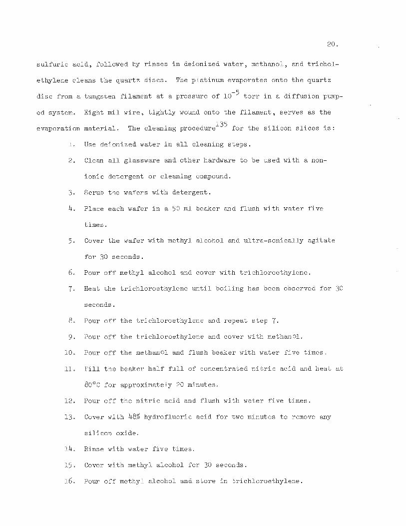
s u l f u r i c a c i d , followed by r i n s e s i n deionized wa te r , methanol, and t r i c h o l -
e thylene c leans t h e q u a r t z d i s c s . The plat inum evaporates onto t h e qua r t z
d i s c from a tungsten f i lament a t a pressure of t o r r i n a d i f f u s i o n pump-
ed system. Eight m i l w i r e , t i g h t l y wound onto t h e f i l a m e n t , se rves a s t h e
evaporat ion ma te r i a l . The c leaning procedure135 f o r t h e s i l i c o n s l i c e s i s :
I, Use deionized water i n a l l c leaning s t e p s .
2 , Clean a l l glassware and o t h e r hardware t o be used wi th a non-
i o n i c de te rgent o r c leaning compound,
3. Scrub t h e wafers wi th de t e rgen t .
4. Place each wafer i n a 50 m l beaker and f l u s h wi th water f i v e
t imes ,
5 , Cover t h e wafer wi th methyl a lcohol and u l t r a - s o n i c a l l y a g i t a t e
f o r 30 seconds.
6. Pour o f f methyl a lcohol and cover wi th t r i c h l o r o e t h y l e n e .
7. Heat t h e t r i c h l o r o e t h y l e n e u n t i l b o i l i n g has been observed f o r 30
seconds.
8 , Pour o f f t h e t r i c h l o r o e t h y l e n e and repea t s t e p 7.
9 . Pour o f f t h e t r i c h l o r o e t h y l e n e and cover wi th methanol.
10. Pour o f f t h e methanol and f l u s h beaker wi th water f i v e t imes"
11, F i l l t h e beaker h a l f f u l l of concent ra ted n i t r i c a c i d and hea t at
8 0 ' ~ f o r approximately 20 minutes,
1 2 Pour o f f t h e n i t r i c ac id and f l u s h with water f i v e t imes.
13. Cover wi th 48% hydro f luo r i c ac id f o r two minutes t o remove any
s i l i c o n oxide ,
14. Rinse wi th water f i v e t imes ,
1 5 , Cover wi th methyl a lcohol f o r 30 seconds,
16 . Pour o f f methyl a lcohol and s t o r e i n t r i c h l o r o e t h y l e n e .

C. Deposition Conditions.
Af te r c leaning and p l ac ing t h e sample i n t h e deposition chamber,
f l u sh ing the system wi th helium gas precedes hea t ing . Af te r hea t ing t h e
sample t o t h e d e s i r e d temperature i n a hydrogen atmosphere f o r t h r e e minutes ,
t h e gases a r e in t roduced a s fo l lows:
3 H2: 530 cm /min
3 . C02: 240 cm /min
3 He across T ~ ( O C H ) : 4600 cm /min
3 7 4
Temperature of T i ( 0 ~ H ) . 100°C 3 7 4 '
Temperature of s u b s t r a t e : 900-950'~
0
Growth r a t e : 100 A/min
Observing t h e co lo r of t h e i n t e r f e r e n c e f r i n g e s g ives t h e f i l m th i ck -
ness during depos i t i on . A t t h e d e s i r e d t h i c k n e s s , t h e He and C02 a r e shu t
o f f , bu t t h e hydrogen remains. Cooling t h e s u b s t r a t e i n hydrogen precedes
a f i n a l helium f l u s h . The commonly used th i ckness i s 2000 angstroms. Evap-
o r a t e d aluminum o r plat inum dots w i th 1 mm2 a r e a form t h e upper meta l e l ec -
t r o d e a t lo-' t o r r , Deposition temperatures ranged from 4 0 0 " ~ t o I O O O ~ C ,
however, t h e f i lms formed a t temperatures below 850°C e x h i b i t poor e l e c t r i c a l
p r o p e r t i e s as shown i n Chapter V and appear by f a s t neutron a c t i v a t i o n analy-
26 s i s t o be oxygen d e f i c i e n t and not s to i ch iome t r i c Ti0 The th i ckness of
2 '
t h e depos i ted f i l m inc reases l i n e a r l y w i th t ime. The depos i t i on r a t e i s con-
s t a n t , s i n c e t h e f i l m i s depos i ted from a chemical reac t ion , and not d i f f u s i o n
l i m i t e d i n t h e s o l i d , as i s t h e case of thermal ly grown oxides. The deposi-
t i o n r a t e i s dependent on t h e flow r a t e s of t h e gases and on t h e temperature
of the organornetall-ic, but i s r e l a t i v e l y independent of t h e s u b s t r a t e temp-
e r a t u r e , This agrees with t h e thermodynamic p red ic t ions of Chapter 111. No
observable d i f f e r e n c e s occur i n t h e depos i t i on of t h e f i l m on plat inum o r
s i l i c o n s u b s t r a t e s .
D, Film Composition,
Fas t neutron a c t i v a t i o n ana lys i s determined t h e s toichiometry of t h e
26 16 f i lms The i r r a d i a t i o n and measurements of N a c t i v i t y used i n t h e oxygen
determinat ion were made a t t h e Texas Nuclear Corporation on a 150 KeV p o s i t i v e
48 ion a c c e l e r a t o r and t h e measurements of t h e Sc a c t i v i t y used i n t h e t i t a n i u m
determinat ion were made wi th a Tr iga Reactor i n t h e Neutron Act iva t ion Analysis
Laboratory of t h e Nuclear Reactor Laboratory of The Univers i ty of Texas a t
Austin. The determinat ion of a c t i v i t y induced i n t i t an iun : i s s imp l i e r be-
cause of t h e longer h a l f - l i f e . Comparison of t h e r a d i o a c t i v i t y produced be-
tween t h a t produced i n t h e depos i ted t h i n f i lms and t h a t i n s tandard mixtures
having known propor t ions of t i t an ium and oxygen determines t h e propor t ion of
t i t an ium and oxygen i n t h e deposit.ed f i l m . The technique has t h e advantage
of be ing r a p i d and non-des t ruc t ive . The technique i s based on t h e p r i n c i p l e
t h a t when a m a t e r i a l i s i r r a d i a t e d by t h e neutrons from a nuc lea r r e a c t o r ,
p a r t i c l e a c c e l e r a t o r , o r o t h e r s u i t a b l e sou rce , some of t h e atoms present i n
t h e m a t e r i a l w i l i i n t e r a c t with t h e neutrons and be converted i n t o d i f f e r e n t
i so topes o f t h e same element o r i so topes of d i f f e r e n t elements depending on
t h e na tu re of t h e i n t e r a c t i o n . I n many cases , t h e i so topes produced a r e
r a d i o a c t i v e , I f each d i f f e r e n t kind of r a d i o a c t i v i t y can be d i s t i ngu i shed o r
s epa ra t ed from a l l t h e r a d i o a c t i v i t i e s produced, t hen t h e amount of each ac t iv -
i t y i s a measure of t h e quan t i t y of t h e parent i s o t o p e p re sen t i n t h e m a t e r i a l .
Meaningful r e s u l t s r e q u i r e t h e presence of a r a t h e r l a r g e quan t i t y of
t i t a n i u m dioxide. Therefore , s p e c i a l samples were prepared with 2 t o 3 m i -
crons of t i t a n i u m dioxide by both t h e low temperature process (550°C) and t,he
high temperature process (85O0c). Addi t iona l 550°C and 850°C samples were
oxid ized i n dry oxygen at 800°C f o r two hours and analyzed. The low tempera-
t u r e samples g ive a r a t i o of Ti:O of about 2 : 3 and suggest t h e presence of
t h e comnpound Ti 0 The high temperature samples and t h e oxid ized samples 2 3 '
g ive a r a t i o of about 1 : 2 and sugges t t h e presence of t he compound Ti0 2"
E. Appearance and S t r u c t u r e .
The depos i ted f i lms appear smooth and r e f l e c t i v e , much l i k e f i lms
of Si02. An x-ray d i f f r a c t i o n powder p a t t e r n i d e n t i f i e s t h e f i l m t o be ti-
tanium dioxide and t h i s , wi th a Laue d i f f r a c t i o n p a t t e r n , shows t h e f i l m t o
be p o l y c r y s t a l l i n e , The f i lms used i n t h e x-ray d i f f r a c t i o n experiments
were approximately one micron t h i c k depos i ted on s i l i c o n .
F* Adherence and S t a b i l i t y .
The Ti0 f i l m adherence t o t h e s u b s t r a t e i s e n t i r e l y s a t i s f a c t o r y . 2
The f i l m does not show any tendency t o p u l l away from t h e s u b s t r a t e during
t h e c l a s s i c "scotch t a p e t e s t " used i n t h e semiconductor i n d u s t r y , The oc-
ca s iona l occurrence of pee l ing dur ing e tch ing i n d i c a t e s t h a t t h e Ti0 i s not 2
a s adherent a s SiO o r Si3N4. Forty-eight p e r cent hydro f luo r i c a c i d 2
e t ches t h e f i l m a t about 700 angstroms p e r minute, The Ti02 f i l m maintains
reproducable e l e c t r i c a l c h a r a c t e r i s t i cs a f t e r prolonged s torange i n a d e s i c-
c a t o r o r i n t h e room atmosphere and a f t e r dunking i n wa te re The f f lms a r e
r e l a t i v e l y hard , b u t a r e not a s r e s i s t a n t t o s c ra t ch ing as SiO o r S i N 2 3 4"
G, Thickness and Refrac t ive Index.
The r e f r a c t i v e index , a s determined by e l l i p somet ry , i s about 2 - 0 .
This i s lower than t h e va lue of 2 .6 f o r r u t i l e 1 9 and i s probably due t o t h e
presence of SiO wi th a r e f r a c t i v e index of 1 . 4 6 a t t h e i n t e r f a c e between 2 '
t h e s i l i c o n and t h e Ti0 However, va lues from 1 .96 t o 2,6 have been r epor t ed 2 "
50363y81,89'90'132 f o r t h e index of r e f r a c t i o n of t h i n f i lms of Ti0 The 2"
e l l i p somete r a l s o determines t h e th i ckness of t h e f i lms . This agrees with t h e
th i ckness determinat ion us ing t h e co lo r of t h e i n t e r f e r e n c e f r i n g e s wi th a
value of 2 .0 f o r t h e index of r e f r a c t i o n . The method of e l l i p somet ry i s non-
d e s t r u c t i v e and capable of extremely high accuracy. El l ipsometry measures
t h e e f f e c t of r e f l e c t i o n on t h e s t a t e of p o l a r i z a t i o n o f l i g h t . The polar -
i z a t i o n s t a t e of l i g h t i s cha rac t e r i zed by t h e phase and amplitude r e l a t i o n s
between t h e two component p lane waves of t h e e l e c t r i c f i e l d vec tor i n t o which
po la r i zed l i g h t may be reso lved . One component ( p ) l i e s i n t h e p lane of in-
cidence and t h e o t h e r component(s) p r o j e c t s normal t o t h e plane of i n c i -
dence. Re f l ec t ion causes a change i n t h e r e l a t i v e phases of t h e p and s
waves and a change i n t h e r a t i o of t h e i r ampli tudes. I n t he Gaertner e l l i p -
someter used h e r e , t h e i n c i d e n t monochromatic l i g h t ( A = 5461 i) passes i n
sequence through t h e c o l l i m a t o r , t h e p o l a r i z e r , and t h e quarter-wave-plate,
The azimuthal o r i e n t a t i o n s o f t h e p o l a r i z e r and t h e quarter-wave-plate de te r -
mine t h e r e l a t i v e amplitudes and phase d i f f e r e n c e between t h e p and s compon-
e n t s of t h e i n c i d e n t beam, These o r i e n t a t i o n s a r e ad jus t ed so t h a t t h e d i f -
fe rence i n phase j u s t compensates t h a t which r e s u l t s from r e f l e c t i o n . The
p lane po la r i zed beam i s then r e f l e c t e d o f f t h e sample at an angle and t r ans -
mi t t ed by t h e ana lyzer through a t e l e s c o p e t o t h e d e t e c t o r . With t h e polar -
i z e r and quarter-wave-plate o r i e n t e d f o r compensation, t h e analyzer i s ad-
j u s t ed t o ex t ingu i sh t h e r e f l e c t e d beam. Then from t h e angles determined by
t h e p o l a r i zer , t h e quarter-wave-plat e , and t h e ana lyzer s e t t i n g s , values of
th ickness and index o f r e f r a c t i o n a r e found us ing t h e SDS 930 research com-
108 p u t e r and a program w r i t t e n by Grady Rylander 111, of t h i s l abo ra to ry . The program o r i g i n a t e s from S n e l l ' s law of r e f r a c t i o n , t h e Murmann-Forsterling
formulae, and t h e F resne l r e f l e c t i o n c o e f f i c i e n t s , and t h e fundamental equa-
92 t i o n of e l l ipsometry o r i g i n a l l y used by McCrackin . This program gives t h e
th i ckness and index of r e f r a c t i o n d i r e c t l y r a t h e r than i n terms of assumed
th i ckness and index of r e f r a c t i o n a s p re sen ted by McCrackin which r equ i r ed
curve f i t t i n g wi th f a m i l i e s of curves. These measurements were used t o
e s t a b l i s h a co lo r cha r t and t o provide a spot check on th i ckness va lues nor-
mally obta ined from t h e co lo r of i n t e r f e r e n c e f r i n g e s ,
H, E l e c t r i c a l Measurements. -
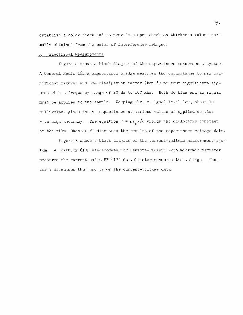
Figure 2 shows a b lock diagram of t h e capaci tance measurement system.
A General Radio 1 6 1 5 ~ capac i tance b r idge measures t h e capac i tance t o s i x s ig -
n i f i c a n t f i g u r e s and t h e d i s s i p a t i o n f a c t o r ( t a n 6 ) t o fou r s i g n i f i c a n t f i g -
u re s wi th a frequency range of 20 Hz t o 100 kHz. Both dc b i a s and ac s i g n a l
must be app l i ed t o t h e sample. Keeping t h e ac s i g n a l l e v e l low, about 10
m i l l i v o l t s , g ives t h e ac capac i tance a t var ious va lues of app l i ed dc b i a s
wi th high accuracy - Th.e equat ion C = r & A/d y i e l d s t h e d i e l e c t r i c cons tan t 0
of t h e f i l m , Chapter VI d i scusses t h e r e s u l t s of t h e capaci tance-vol tage d a t a ,
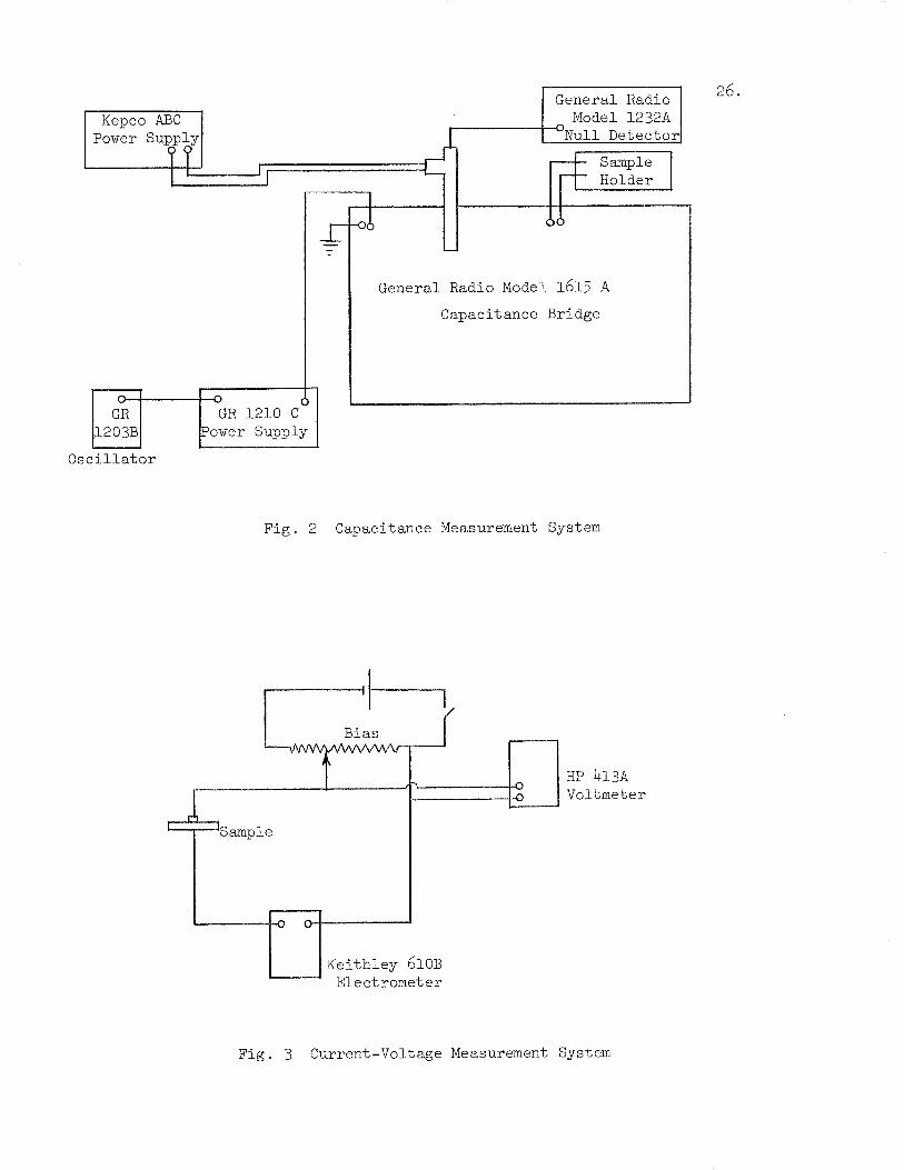
Figure 3 shovs a block diagram of t h e cur ren t -vol tage measurement sys-
tem, A Kei th ley 6 1 0 ~ e l ec t rome te r o r Hewlett-Packard 4 2 5 ~ micromicroammeter
measures t h e cur ren t and a HP 4 1 3 ~ dc vol tmeter measures t h e vol tage . Chap-
t e r V d i scusses t h e resu- l t s of t h e current-vol tage d a t a ,
I General Radio I Model 1232A
General Radio Model 1615 A
Capacitance Bridge
O s c i l l a t o r
F ig . 2 Capacitance Measurement System
Bias I
Kei th ley 6 1 0 ~ Electrometer
HP 4 1 3 ~ Voltmeter
F ig . 3 Current-Voltage Measurement System

CHAPTER V.
CONDUCTION PROPERTIES OF TITANIUM DIOXIDE
A , Conduction Mechanisms :
Conduction p r o p e r t i e s i n t h i n d i e l e c t r i c f i lms have been s t u d i e d
ex tens ive ly i n r ecen t yea r s 34 947 ,93,94,96,117,137. A large number of
nea r ly amorphous i n s u l a t i n g m a t e r i a l s a r e known which, when a high e l e c -
t r i c f i e l d i s app l i ed t o t h i n f i lms of t h e subs tance , e x h i b i t a cu r r en t
f law wht ch i n r re ases roughly exponent ia l ly with app l i ed v o l t age over many
decades, The vol tage r equ i r ed f o r a given cu r ren t i n many of t h e s e mater-
i a l s decreases monotonically with absolu te tempera ture . Current mechanisms
whlch might e x i s t i n t h i n f l l m d i e l e c t r i c s inc lude i o n i c flow, t unne l ing ,
space charge l i m i t e d flow wi th d i s t r i b u t e d t r a p s , Schot tky emission, and
Poole-Frenkel emission,
imperfect ions i n any r e a l m a t e r i a l allow s t a t e s t o e x i s t i n t h e
forbidden band, These s t a t e s ( t r a p s ) a f f e c t t h e conduction process by cap-
t u r i n g and emi-tt ing c a r r i e r s t o t h e conduction and valence bands. I n i n -
s u l a t o r s , t r a p s c o l l e c t i n g c a r r i e r s compensate f o r t r a p s c o n t r i b u t i n g f r e e
c a r r i e r s t o t h e conduction p roces s , i . e . , acceptor t r a p s compensate donor
t r a p s . I n s u l a t i n g m a t e r i a l s wLth a l a r g e number of l o c a l i z e d s t a t e s
( t r a p s ) remain i n s u l a t i n g because of a high degree of compensation, o r t h e
energy d i f f e rence between t h e t r a p s and t h e nea re r band i s l a r g e compared t o
t ,be thermal energy a
S i g n i f i c a n t current, may flow i n i n s u l a t o r s a t high temperatures and
h igh f i e l d s due t o t h e i n c r e a s i n g quan t i t y of f r e e c a r r i e r s . The c a r r i e r
in , jee t ion mechanism determines t o a l a r g e ex ten t t h e e l e c t r i c p r o p e r t i e s of
t h e m a t e r i a l and i s t h e r e f o r e of g r e a t importa,nce t o device designers , Con-
s i d e r now some of t hese c ~ n d u c t ~ i o n mechanisms:
28.
1. I o n i c Flow.
I n an i o n i c c r y s t a l , such as t h e a l k a l i h a l i d e s , cu r r en t s occur a s a
44 r e s u l t o f t h e migra t ion of ions under t h e in f luence of an e l e c t r i c f i e l d ,
s i m i l a r t o t h e e l e c t r o l y t i c conduction of aqueous s o l u t i o n s of s a l t s . I o n i c
conduction would e x h i b i t an exponent ia l volt-ampere c h a r a c t e r i s t i c and a de-
c reas ing vol tage-temperature character is ti^^^. Maserjian and MeanY0 i n t e r -
p r e t t h e i r r e s u l t s on evaporated t h i n f i lms (100-400 ;) of Ti0 i n terms of 2
a l a r g e i o n i c space charge i n t h e Ti0 f i lms . For i o n i c conduction t h e t r a n - 2
s i e n t t ime f o r i o n s should be q u i t e l a r g e and t h e r e should be a t r a n s p o r t o f
m a t e r i a l from one e l e c t r o d e t o t h e o t h e r . I o n i c flow i s e l imina ted a s a pos-
s i b l e mechanism i n t h i s work because l a r g e c u r r e n t s were maintained i n t h e
samples f o r extended per iods of t ime without observa t ion of cu r r en t decay
due t o i o n i c build-up near an e l e c t r o d e . One should note mechanical changes
o r p l a t i n g of one e l e c t r o d e m a t e r i a l on to t h e o t h e r e l ec t rode i f i o n i c cur-
r e n t s were p r e s e n t . Also , it i s gene ra l ly be l i eved t h a t i o n i c c u r r e n t s of
t he r equ i r ed magnitude t o expla in t h e r e s u l t s i n t h i n f i lms could not be sup-
9 3 por t ed i n t h i n f i lms f o r more than an i n s t a n t without m a t e r i a l breakdown . 2 . Tunneling.
Tunneling occurs when t h e b a r r i e r becomes t h i n enough f o r appreci-
ab l e q u a n t i t i e s of e l e c t r o n s t o p e n e t r a t e t h e b a r r i e r and emerge t o t h e o t h e r
s ideg4 "I8 y123. Figure 4 shows t h r e e ways tunnel ing occurs :
( a ) Tunneling from t h e conduction band of t he metal i n t o t h e con-
duc t ion band of t h e i n s u l a t o r ;
( b ) d i r e c t tunnel ing from t h e conduction band of one metal i n t o t h e
conduction band of t h e o t h e r ;
( c ) t unne l ing from t h e valence band of t h e i n s u l a t o r d i r e c t l y i n t o
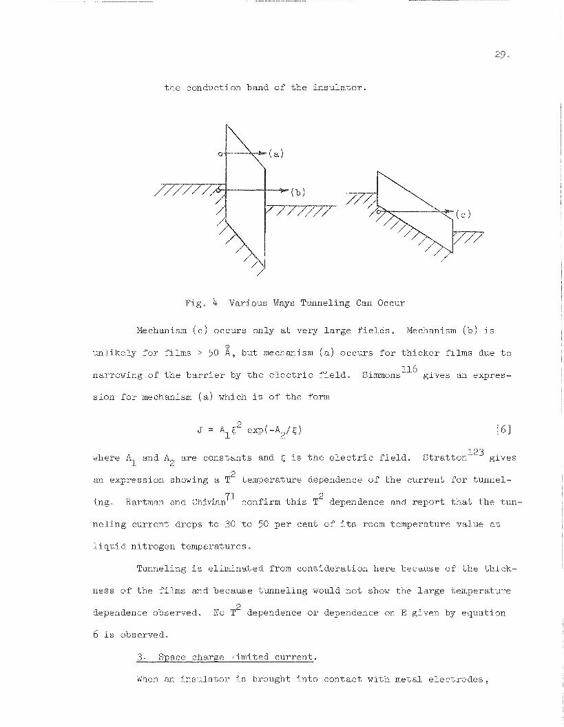
t h e conduction band of t h e i n s u l a t o r .
F i g , 4 Various Ways Tunneling Can Occur
Mechanism ( c ) occurs only a t very l a r g e f i e l d s . Mechanism ( b ) i s
0
u n l i k e l y f o r f i lms > 50 A , b u t mechanism ( a ) occurs f o r t h i c k e r f i lms due t o
narrowing of t h e b a r r i e r by t h e e l e c t r i c f i e l d . Simrnons116 g ives an expres-
s ion f o r mechanism ( a ) which i s of t h e form
where A and A a r e cons tan ts and 6 i s t h e e l e c t r i c f i e l d . s t r a t t o n L e 3 g ives 1 2
Z an expression showing a T temperature dependence of t h e cu r r en t f o r tunnel -
2 i ng . Hartman and chiv%an7l confirm t h i s T dependence and r e p o r t t h a t t h e tun-
n e l i n g cur ren t drops t o 30 t o 50 p e r cent of i t s room temperature va lue a t
l i q u i d n i t rogen temperatures .
Tunneling i s e l imina ted from cons idera t ion here becaduse of t he th i ck -
ness of t h e f i b s and because tunnel ing would not show t h e l a r g e teniperature
2 dependence observed. No T dependence o r dependence on E given by equat ion
6 i s observed.
3. Space charge l i m i t e d cu r r en t .
When an i n s u l a t o r i s brought i n t o con tac t wi th metal e l e c t r o d e s ,
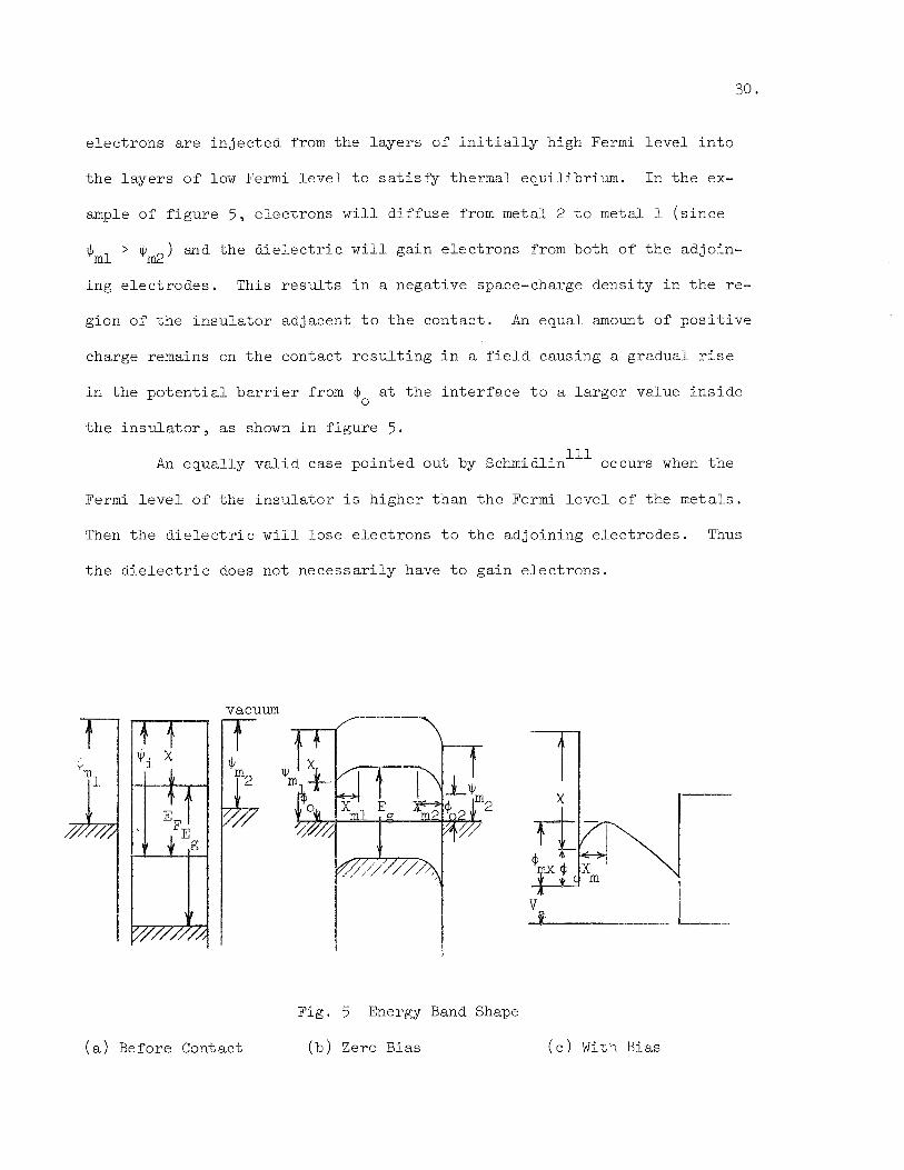
e l e c t r o n s a r e i n j e c t e d from t h e l a y e r s of i n i t i a l l y high Fermi l e v e l i n t o
t h e l a y e r s o f low Fermi Level t o s a t i s f y thermal equi l ibr ium. I n t h e ex-
ample of f i g u r e 5 , e l ec t rons w i l l d i f f u s e from metal 2 t o metal 1 ( s i n c e
* m l > ) and t h e d i e l e c t r i c w i l l g a i n e l e c t r o n s from both of t h e adjoin-
i ng e l e c t r o d e s . This r e s u l t s i n a nega t ive space-charge dens i ty i n t h e re-
gion of t h e i n s u l a t o r ad jacent t o t h e con tac t . An equal amount of p o s i t i v e
charge remains on t h e contac t r e s u l t i n g i n a f i e l d causing a gradual r i s e
i n t h e p o t e n t i a l b a r r i e r from 4 a t t h e i n t e r f a c e t o a l a r g e r value i n s i d e 0
t h e i n s u l a t o r , a s shown i n f i g u r e 5 .
An equa l ly v a l i d case po in t ed out by ~ c h m i d l i n l ' l occurs when t h e
Fermi l e v e l o f t h e i n s u l a t o r i s h ighe r than t h e Fermi l e v e l of t h e meta ls .
Then t h e d i e l e c t r i c w i l l l o s e e l e c t r o n s t o t h e ad jo in ing e l e c t r o d e s . Thus
t h e d i e l e c t r i c does not n e c e s s a r i l y have t o ga in e l e c t r o n s .
F ig . 5 Energy Band Shape
( a ) Before Contact ( b ) Zero Bias ( c ) With Bias

The a p p l i c a t i o n of a b i a s t o t h e system r e s u l t s i n t h e appearance of
an a ,ddi t ional p o s i t i v e charge on t h e anode and an equal amount of nega t ive
5 2 charge i n t h e i n s u l a t o r a s a space charge . It i s t h i s space charge which
c a r r i e s t h e c u r r e n t . The charge d i s t r i b u t i o n i n t h e system under appl ied
b i a s c o n s i s t s of a p o s i t i v e charge on t h e cathode o r i g i n a t i n g from thermal
equi l ibr ium requirements , a p o s i t i v e charge on t h e anode maintained by t h e
app l i ed b i a s , and a nega t ive space charge i n t h e i n s u l a t o r equal i n magni-
t ude t o t h e sum of t h e p o s i t i v e charges on t h e cathode and anode.
The cu r ren t flow i n t h e system descr ibed above i s space charge l i m -
i t e d with t h e cu r r en t i n t h e cathode region flowing p r imar i ly by d i f f u s i o n
and tha,t i n t h e anode reg ion p r imar i ly by d r i f t . For an unl imi ted supply of
c a r r i e r s , t h e express ion f o r one -ca r r i e r , t r a p - f r e e , space charge l i m i t e d
cu r r en t (SCLC) i s of t h e form 52
I n gene ra l , t h e assumption of an unl imi ted supply of c a r r i e r s does no t ho ld
2 and t r a p s cause important e f f e c t s on the c u r r e n t . This V dependence i s not
observed f o r t h e s e T i 0 f i l m s . 2
Space charge l i m i t e d cu r r en t s a f f e c t t h e f i e l d d i s t r i b u t i o n which i n
t u r n a f f e c t s t h e i n j e c t i o n p roces s . Frank and ~ i m m o n s ~ ~ consider t h e e f -
f e c t s of space charge on emission-l imited c u r r e n t flow i n i n s u l a t o r s , They
f i n d t h a t a f t e r t h e cu r r en t reaches t h e va lue i n equat ion 7 , as t h e vo l t age
i s i nc reased , r e s u l t i n g i n an inc reas ing negat ive charge i n t h e i n s u l a t o r ,
p o s i t i v e charge i s removed flom t h e cathode, reducing t h e b a r r i e r he igh t $I max
a t t he meta l - insu la tor i n t e r f a c e , and al lowing more cu r r en t t o flow. When
t h i s p o s i t i v e charge i s dep le t ed , 4 i s equal t o 4 and t h e con tac t i s no max o '
longer ohmic and emission l i m i t e d cu r r en t s e t s i n . Negative charge now be-
g ins t o appear on t h e cathode, a s w e l l a s i n t h e i n s u l a t o r and t h e contact,
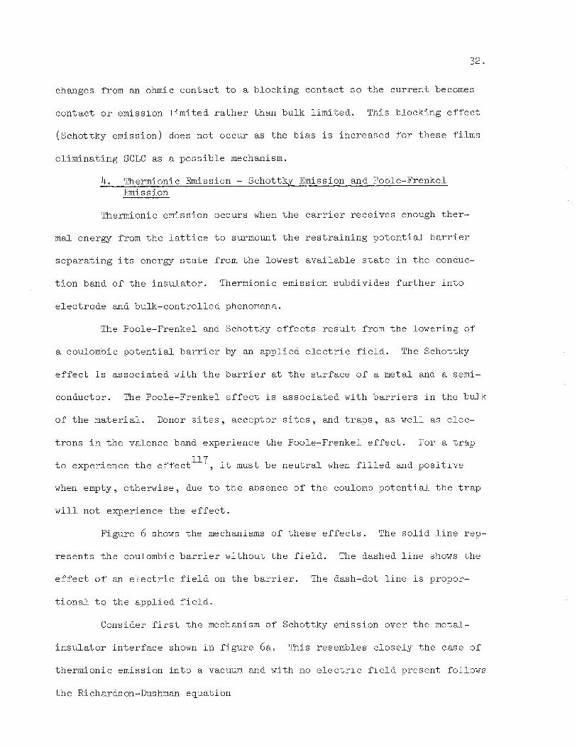
changes from an ohmic con tac t t o a blocking contac t s o t h e cu r r en t becomes
con tac t o r emission l i m i t e d r a t h e r t han bulk l i m i t e d . This blocking e f f e c t
(Schottky emission) does n o t occur a s t h e b i a s i s i nc reased f o r t h e s e f i lms
e l imina t ing SCLC as a p o s s i b l e mechanism.
4. Thermionic Emission - Schottky Emission and Poole-Frenkel Emission
Thermionic emission occurs when t h e c a r r i e r r ece ives enough the r -
mal energy from t h e l a t t i c e t o surmount t h e r e s t r a i n i n g p o t e n t i a l b a r r i e r
s e p a r a t i n g i t s energy s t a t e from t h e lowest a v a i l a b l e s t a t e i n t h e conduc-
t i o n band of t h e i n s u l a t o r . Thermionic emission subdivides f u r t h e r i n t o
e l e c t r o d e and bulk-cont ro l led phenomena.
The Poole-Frenkel and Schottky e f f e c t s r e s u l t from t h e lowering of
a coulombic p o t e n t i a l b a r r i e r by an app l i ed e l e c t r i c f i e l d . The Schottky
e f f e c t i s a s soc i a t ed wi th t h e b a r r i e r a t t h e su r f ace of a metal and a semi-
conductor. The Poole-Frenkel e f f e c t i s a s s o c i a t e d wi th b a r r i e r s i n t h e bulk
of t h e m a t e r i a l . Donor s i t e s , acceptor s i t e s , and t r a p s , a s w e l l a s e l ec -
t r o n s i n t h e valence band experience t h e Poole-Frenkel e f f e c t . For a t r a p
t o experience t h e effect117, it must be n e u t r a l when f i l l e d and p o s i t i v e
when empty, o therwise , due t o t h e absence of t h e coulomb p o t e n t i a l t h e t r a p
w i l l no t experience t h e e f f e c t . Figure 6 shows the mechanisms of t h e s e e f f e c t s . The s o l i d l i n e rep-
r e s e n t s t h e coulombic b a r r i e r wi thout t h e f i e l d . The dashed l i n e shows t h e
e f f e c t o f an e l e c t r i c f i e l d on t h e b a r r i e r . The dash-dot l i n e i s propor-
t i o n a l t o t h e appl ied f i e l d .
Consider f i r s t t h e mechanism of Schottky emission over t h e metal-
i n s u l a t o r i n t e r f a c e shown i n f i g u r e 6a . This resembles c lo se ly t h e case o f
thermionic emission i n t o a vacuum and with no e l e c t r i c f i e l d present fol lows
t h e Richards on-Dushman equat ion
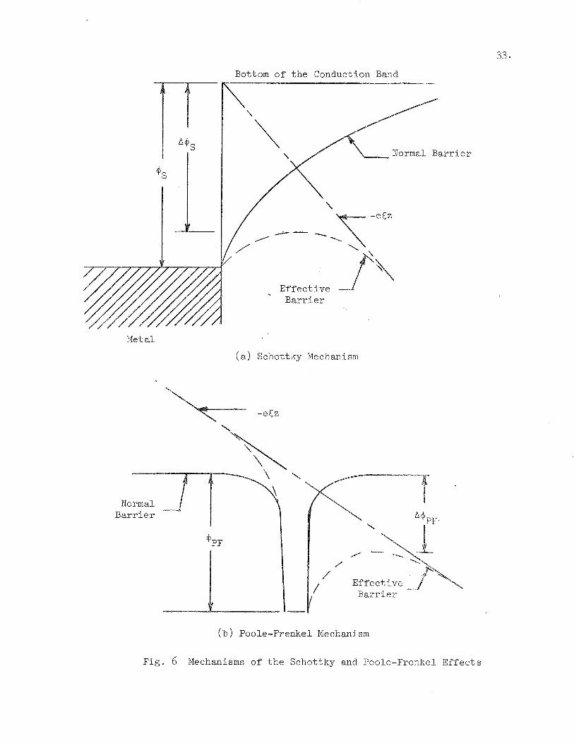
Bottom of the Conduction Band
Metal
(a) Schottky Mechanism
L I
I /
/ / Effective
(b) Poole-Frenkel Mechanism
Fig. 6 Mechanisms of the Schottky and Poole-Frenkel Effects

2 J = AST exp ( - + S / k ~ )
where
The thermionic cu r r en t i s n e g l i g i b l e a t normal temperature. However,
a p p l i c a t i o n of an e l e c t r i c f i e l d lowers t h e b a r r i e r he igh t and inc reases t h e
cu r r en t by g iv ing t h e e l e c t r o n s a d d i t i o n a l a c c e l e r a t i o n . The emi t ted e lec-
t r o n sees an e l e c t r o s t a t i c f o r c e of a t t r a c t i o n between i t s e l f and t h e emis-
s i o n su r f ace caused by t h e image charge appearing wi th in the conducting sur -
face when t h e e l e c t r o n i s emi t t ed , a s shown i n f i g u r e 7a. The magnitude of
t h i s image f o r c e , i s
e F = 2 newtons 4 n ~ ~ ~ ( 2 z )
An app l i ed e x t e r n a l e l e c t r i c f i e l d e x e r t s a fo rce on t h e e l e c t r o n
given by
F = q5
This r e s u l t s i n a b a r r i e r lowering given by
r e s u l t i n g i n an e f f e c t i v e ba . r r ie r
which gives t h e equat ion f o r Schottky emission a s
2 J S = AsT exp [ - (4S - n $ , ) / k ~ l [I1& 1
The proper d i e l e c t r i c cons tan t i s t h e e l e c t r o n i c component ( square of
t h e index of r e f r a c t i o n ) s i n c e t h e e l e c t r o n i s immediately c o l l e c t e d by t h e
f i e l d and does not p o l a r i z e t h e ions i n t h e v i c i n i t y .
Consider now t h e Poole-Frenkel mechanism. Deviations i n t h e s lope
of t h e l o g J vs . curves from t h e value p red ic t ed by Schottky emission
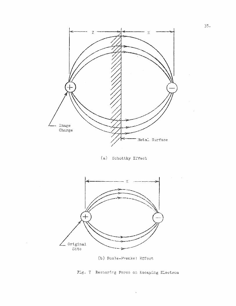
Charge
Metal Surface
( a ) Schot tky Ef fec t
(b) Poole-Frenkel Ef fec t
F ig . 7 Restor ing Force on Escaping Electron

36.
(equat ion 1 4 ) a r e expla ined by a model f i r s t proposed by ~ r e n k e l ~ ~ based on
i n t e r n a l , f i e l d a s s i s t e d , thermal emission. Seve ra l au thors 54,77 ,93,124 find
46 t h a t it b e s t exp la ins t h e i r da t a . Recent ly, 0'Dwyerlo2 and Emtage i n t r o -
duced new models, based on tunne l ing mechanisms, which at tempt t o account f o r
t h e s l o p e d i f f e r ences . A recent paper by ~ i m r n o n s l ~ ~ cons ider ing a Poole-
Frenkel type model wi th n e u t r a l t r a p s l y i n g above t h e Fermi l e v e l and donor
s t a t e s l y i n g below t h e Fermi l e v e l , s i g n i f i c a n t l y c l a r i f i e s t h e theory . Hu,
e t i n a s h o r t paper , modified t h e Poole-Frenkel model t o account f o r
d i f f e r ences i n t h e s lopes o f t h e l o g 5 v s . g1I2 curves. ~ e a r g a n l ~ ~ extended
t h e Poole-Frenkel model t o inc lude t h e e f f e c t s of compensation showing t h a t
t h e r e l a t i v e d e n s i t i e s of donor and acceptor s i t e s c o n t r o l t h e s lope of t h e
l o g J vs . t1l2 p l o t s .
The cu r ren t dens i ty express ion f o r Poole-Frenkel emission a r i s e s from
t h e express ion f o r t h e conduct iv i ty of a m a t e r i a l
~ = n e u ohm-cm [15 1
The concent ra t ion of f r e e e l e c t r o n s i n t h e m a t e r i a l i s
n = n exp (-$/rkT) 0
[16 I
where r i s a parameter ranging between 1 and 2 depending on t h e r e l a t i v e den-
s i t i e s o f donors and accep to r s . The p o t e n t i a l d i f f e r e n c e , +, e x i s t s between
t h e t r a p l e v e l and t h e lowest s t a t e i n t h e conduction band. Using t h e energy
band model wi th a s i n g l e l e v e l each f o r donor and acceptor t r a p s i n t h e f o r -
bidden band of t h e i n s u l a t o r , t h e concent ra t ion of f r e e c a r r i e r s f o r an in-
t r i n s i c m a t e r i a l i s 119
n = ( N N )1'1 exp [ - ( E ~ - Ev)/2kT] C V
For n-type m a t e r i a l wi th no acceptor s i t e s 1x9
NcNd 112 n = (-) 2 exp [-(Ec - E ~ ) / B ~ T ] = nl exp (-$/2kT)
where N a < < N N < < n . d ' a
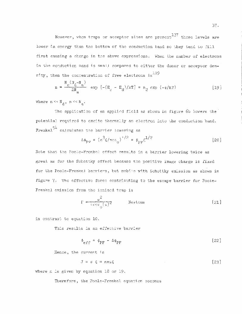
However, when t r a p s o r acceptor s i t e s a r e present137 t h e s e l e v e l s a r e
lower i n energy than t h e bottom of t h e conduction band s o they t e n d t o f i l l
f i r s t causing a change i n t h e above express ions . When t h e number of e l e c t r o n s
i n t h e conduction band i s smal l compared t o e i t h e r t he donor o r acceptor den-
s i t y , then t h e concent ra t ion of f r e e e l e c t r o n s i s 119
where n < < ? J n c < N . d ' a
The app l i ca t son of an app l i ed f i e l d a s shown i n f i g u r e 6b lo~&re r s t h e
p o t e n t i a l r equ i r ed t,o e x c i t e thermal ly an e l e c t r o n i n t o t h e conduction band.
FrenkelS4 c a l c u l a t e s t h e b a r r i e r lowering as
Note t h a t t h e Poole-Frenkel e f f e c t r e s u l t s i n a b a r r i e r lowering tw ice a s
g r e a t a s f o r t h e Schottky e f f e c t because t h e p o s i t i v e image charge i s f i x e d
f o r t h e Poole-Frenkel b a r r i e r s , bu t mobile wi th Schottky emission as shown i n
f i g u r e 7, The e f f e c t i v e fo rce c o n t r i b u t i n g t a t h e escape b a r r i e r f o r Poole-
Frenkel emission from t h e ion ized t r a p i s
Newtons
i n c o n t r a s t t o equat ion 10 .
This r e su - l t s i n an e f f e c t i v e b a r r i e r
- 'eff ~ P F - ' ~ P F
Hence, t h e cu r r en t i s
J =: a 5 = newt
where n i s given by equat ion 1 8 o r 19 .
Therefore , t.he Poole-Frenkel equat ion becomes
Case I N < < N N < < n a d ' a
JpF = eunlE exp [-(4PF - A4pF)/2kTl
Case I1 n c.< N n << Na d '
JpF = em2E exp [-(4PF - A 4 p F ) / k ~ l
These equat ions may be w r i t t e n a s
- JpF - ao< exp (A4pF/2k~) = 'Jot exp ( A ~ ~ I ~ T T )
wi th only one type of s i t e p r e s e n t , and
wi th compensation, where a = neu. 0
Therefore, both t h e Poole-Frenkel and Schottky mechanisms y i e l d
s t r a i g h t l i n e s on p l o t s o f l o g J vs . E l l 2 and both may e x h i b i t t h e same s lope
on t h e s e p l o t s depending on condi t ions wi th in t h e i n s u l a t o r . Both e f f e c t s a r e
l i k e w i s e exponent ia l ly dependent on 1/T. These c r i t e r i a a r e then i n s u f f i c i e n t
f o r vnique i d e n t i f i c a t i o n 137,
Rewriting t h e Schottky equat ion as
no te t h a t J i s exponen t i a l l y dependent on t h e b a r r i e r he igh t a t t h e metal-in- 0
s u l a t o r i n t e r f a c e ( f i g u r e 6 ) while a i s exponent ia l ly dependent on t h e bar- 0
r i e r of t h e donor s i t e s w i t h i n t h e i n s u l a t o r . Therefore , t h e cu r r en t charac-
t e r i s t i c s of M I M devices u s ing metals with d i f f e r e n t work func t ions w i l l be
h igh ly asymmetric f o r Schottky emission and symmetric f o r Poole-Frenkel emis-
s i o n .
The b a r r i e r h e i g h t can f u r t h e r v e r i f y t h e presence o f Schottky emis-
70 s i o n . The o r d i n a t e i n t e r c e p t of a l o g J vs . p l o t y i e l d s ( and t h e S
2 s lope of a p l o t of l o g J /T vs . 1/T y i e l d s $s - A$s, however, equat ion 12
gives A+ . The b a r r i e r $ should agree when obtained by t h e s e two methods. S S
For Poole-Frenkel emission, ana lys i s of t h e l o g 5 vs . l 2 curves be-
g ins by not ing t h e l i m i t i n g slope values of
wi th donors only p resen t , and
wi th compens a t i on,
An independent measure of E , t h e high frequency d i e l e c t r i c cons tan t ,
then determines i f compensation i s p resen t . A knowledge of t h e degree of com-
pensat ion now allows the b a r r i e r he ight $ t o be determined. Biasing t h e di- PF
e l e c t r i c t o a s u i t a b l e value of cu r ren t and varying t h e temperature a t a con-
s t a n t b i a s y i e l d s da ta which e x h i b i t s a s t r a i g h t l i n e p l o t of log I versus 1 / T .
The s lope of t h i s l i n e i s propor t ional t o t h e a c t i v a t i o n energy, E from d
The a c t i v a t i o n energy i s r e l a t e d t o t h e b a r r i e r he ight by
where r = 2 with donors only present and r = 1 with compensation. A knowledge
of the degree of compensation, r , obtained by comparing t h e measured s lope
wi th t h e l i m i t i n g values from equations 29 and 30 and t h e b a r r i e r he igh t gives
information about t h e dens i ty of t r a p s . The i n t e r c e p t of t h e log o versus 5 112
curve i s a measure of 5 which i s a funct ion of t h e t r a p dens i ty . The b a r r i e r 0 '
height of the t r a p s r e s u l t s from t h e l o g I versus 1 / T v a r i a t i o n .
B. Experimental Resul t s and Discussion.
124 ~ e a d ~ ~ , with Ta 0 f i lms , and Sze , with Si3N4, i d e n t i f y t h r e e com-
2 5
ponents of current . They f i n d t h a t a ) Poole-Frenkel o r i n t e r n a l Schottky emis-
s ion dominates a t high f i e l d s and high temperatures, b ) f i e l d ion iza t ion domi-
na te s a t high f i e l d s and low temperatures, and c ) thermal hopping of c a r r i e r s
from one i s o l a t e d s t a t e t o another dominates a t low f i e l d s and moderate tem-
pe ra tu res . The thermal hopping mechanism y i e l d s an ohmic c h a r a c t e r i s t i c , ex-
ponen t i a l ly dependent on temperature, but ~ e a d ~ ~ s t a t e s t h a t a t higher tempera-
t u r e s , t h i s mechanism would normally be expected t o con t r ibu te much l e s s cur-
r en t than mechanism ( a ) . The f i e l d ion iza t ion mechanism y i e l d s a current-
vol tage c h a r a c t e r i s t i c independent of temperature. Figure 8 shows t h e cu r ren t
v a r i a t i o n with temperature f o r these devices y i e l d i n g an a c t i v a t i o n energy of
0.11 eV. Mead suggests t h a t such a low a c t i v a t i o n energy might be due t o some
e lec t ron hopping from one t r a p t o another with low mobi l i ty . However, no
ohmic behavior i s observed experimentally t o support t h i s suggestion. This
exponential dependence of t h e current on temperature i s f u r t h e r evidence t h a t
tunnel ing i s not observed here .
Figure 9 shows thak experimentally t h e current i s propor t ional t o exp
(m5 'I2) where m i s a constant and 5 t h e e l e c t r i c f i e l d . This behavior can be
explained e i t h e r on t h e b a s i s of Schottky emission (equation 1 3 ) o r Poole-
Frenkel emission (equat ions 24 and 2 5 ) . Schottky emission depends s t rongly on
t h e b a r r i e r between t h e metal and i n s u l a t o r and should vary with t h e metal
work funct ion. Figure 9 shows t h a t such dependence does not appear experi-
mentally f o r M I M s t r u c t u r e s . I f Schottky emission dominates, a d i f f e rence of
only 0.06 eV i n t h e b a r r i e r he ights a t t h e two meta l - insula tor - in ter faces r e -
s u l t s i n a decade of cu r ren t d i f ference a t equal and opposi te f i e l d s . The de-
v ice of f i g u r e 9 has plat inum and aluminum e lec t rodes which have a work
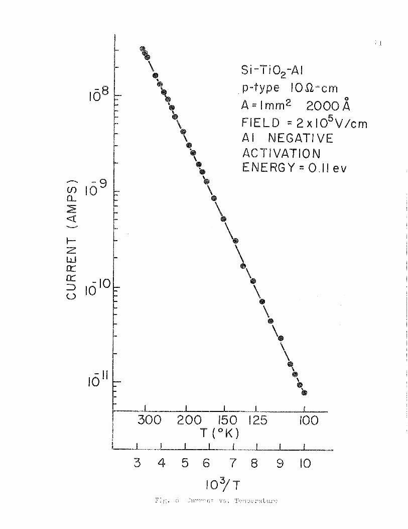
p-type IOQ-cm
A = lmm2 2000A FIELD = 2 x 1 0 5 ~ / c m A l NEGATIVE ACTIVATION ENERGY = 0.11 e v
T ( " K
1 . Cur ren t vs . 'I'e~:iperr?.t:::-:?
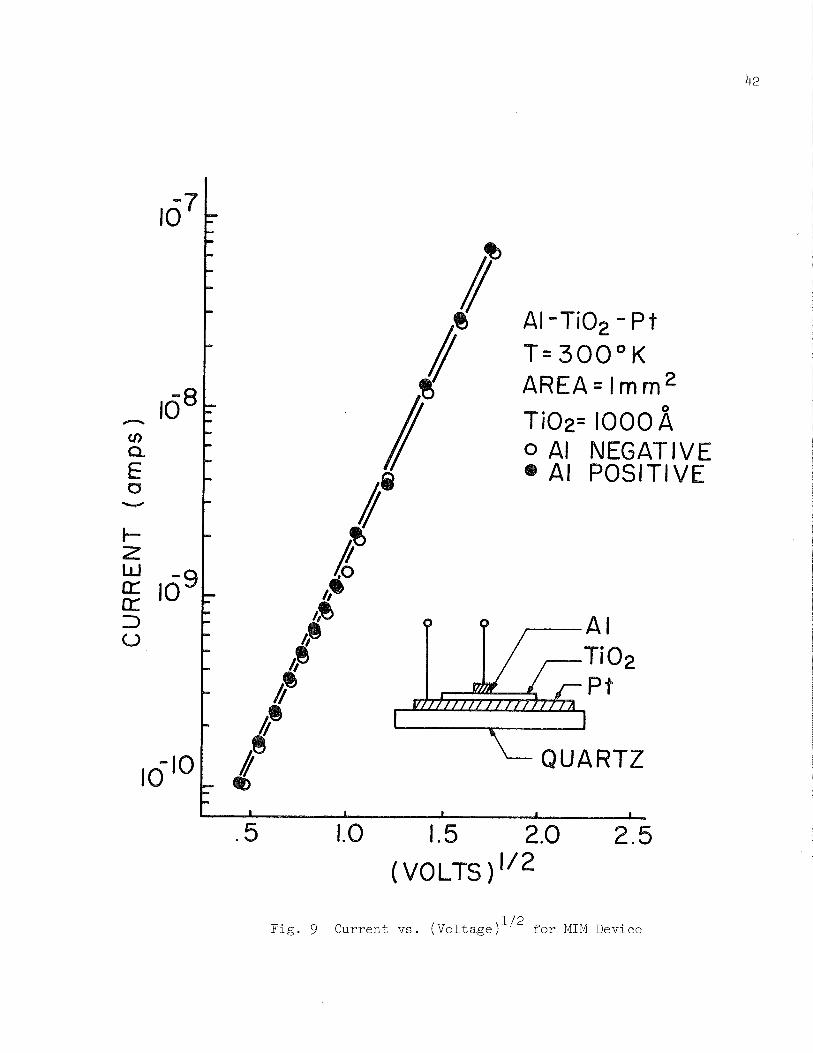
TiO2= 1000 f i 0 Al NEGATIVE @ A l POSITIVE
QUARTZ
( VOLTS ) 1 / 2
Fig . 9 Current vs. f o r M I M Device
func t ion d i f f e r ence of approximately 1 eV. The Poole-Frenkel e f f e c t i s as-
s o c i a t e d with b a r r i e r s i n t h e bulk of t h e m a t e r i a l , and t h e p o l a r i t y inde-
pendence, exponent ia l dependence wi th 1/T, and exponent ia l dependence wi th
vl/*, imply t h a t Poole-Frenkel i s d e f i n i t e l y t h e dominant mechanism,
Figure 10 p re sen t s t h e vol tage r equ i r ed t o produce l o - ' amperes
through f i lms of var ious th i cknesses . AccorCiing t o ~ e a d ~ ~ , t h e l i n e a r i t y of
such a p l o t i n d i c a t e s t h a t t h e observed cu r ren t s a r e not space-charge l i m -
i t e d due t o t r a p s , The space-charge l i m i t e d c u r r e n t f o r a quasi-continuum
of t r app ing s t a t e s between t h e Fermi l e v e l and t h e conduction band i s non-
l i n e a r i n terms of f i l m th i ckness . Also, any model i n which t h e e l ec t rodes
cause r a t e l i m i t i n g i n t h e t r a n s p o r t process p r e d i c t s a dev ia t ion from l i n e -
a r i t y due t o low mob i l i t y . ~ e a d ~ ~ concludes t h a t t h e l i n e a r i t y of such a p l o t
impl ies t h a t t he bulk of t h e m a t e r i a l l i m i t s t h e c u r r e n t and not -:he p o t e n t i a l
b a r r i e r s a t t h e e l e c t r o d e s , Also, t h e passage of t h i s curve through t h e o r i -
g in d e f i n i t e l y impl ies a bu lk c o n t r o l l e d mechanism.
On MIS devices ( f i g u r e 11) a p o l a r i t y d i f f e r e n c e e x i s t s , sugges t ing
a p e n e t r a t i o n of t h e e l e c t r i c f i e l d i n t o a su r f ace o r dep le t ion l a y e r of t h e
semiconductor wi th r eve r se b i a s , r a t h e r than v a r i a t i o n s i n t h e b a r r i e r h e i g h t s .
I n t h e forward d i r e c t i o n , t h e f i e l d w i th in the i n s u l a t o r dominates t h e cus-
rent which inc reases e x p o n e n t i d l y wi th b i a s vo l t age as f o r t h e Poole-Frenkel
e f f e c t .
~ a , n ~ ~ ~ ~ r e c e n t l y s t u d i e d t h i s s a t u r a t i o n e f f e c t wi th r eve r se b i a s f o r
a metal-polymer-sil icon (n- type) ( M P S ) s t r u c t u r e us lng polymerized s l l i c o n e
d i f f u s i o n pump o i l and i n t e r p r e t e d t h e r e s u l t s i n terms of t h e p ropor t ion of
t h e vol tage drop ac ros s t h e polymer and t h e semiconductor t o zhe t o t a l b i a s
volta,ge. J.D, T r o t t e r , of t h i s l a b o r a t o r y , proposed a model whereby t h e gen-
e r a t i o n of e lec t ron-hole p a i r s i n t h e dep le t ion l a y e r of the semiconductor
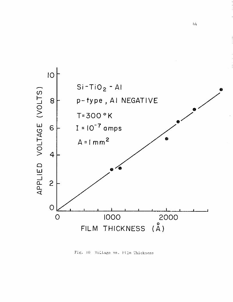
p- t y p e , A I NEGATIVE
T=300°K
I = amps
A = l m m 2
1000 2000
FILM THICKNESS (i)
Fig. 10 Voltage vs. Film Thickness
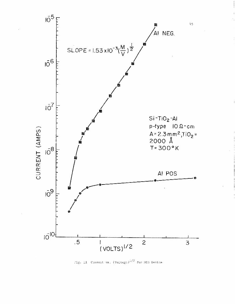
-
I NEG.
i SLOPE = 1.53 x iQ-
S i -Ti02 -A1 p-type 18 Q-cm
Fig. II Current vs. (Voltage)"* for MIS Device

l i m i t s t h e cu r r en t flow i n t h e r eve r se b i a s condi t ion causing s a t u r a t i o n .
Two "impedances" corresponding t o t h e vo l t age drop across t h e d i e l e c t r i c and
semiconductor a r e a s soc i a t ed wi th t h e MIS device. A t low b i a s , e s s e n t i a l l y
a l l t he app l i ed vol tage appears across t h e d i e l e c t r i c . As t h e r eve r se b i a s
i n c r e a s e s , t h e drop ac ros s t h e semiconductor begins t o appear a s t h e semicon-
duc tor forms a dep le t ion l a y e r . A t some v o l t a g e , t h e impedance of t h e semi-
conductor i n c r e a s e s t o a value equal t o t h a t of t h e d i e l e c t r i c and t h e v o l t -
age i s shared equa l ly between them. The rea f t e r , more of t h e vol tage f a l l s
across t h e semiconductor, Figure 11 shows t h a t t h i s s a t u r a t i o n begins t o oc-
cu r f o r Ti02 a t approximately 0 .5 v o l t which, as w i l l be shown i n Chapter V I ,
i s a t l e a s t a s g r e a t a s t h e vol tage t h a t t h e capaci tance-vol tage curve shows
f o r t h e formation of an invers ion l a y e r , The formation of an inve r s ion l a y e r
causes t h e capac i tance t o approach a minimum value . Actua l ly , t h e r e i s a
f i e l d induced p-n junc t ion a t t h e semiconductor s u r f a c e . For t h e case o f
an^^^^, us ing n-type m a t e r i a l , t h i s p-n junc t ion causes i n j e c t e d e l e c t r o n s
from t h e negat ive vol tage on t h e i n s u l a t o r e l e c t r o d e t o combine wi th t h e ho le s
i n t h e inve r s ion l a y e r , U n t i l t h e i nve r s ion l a y e r becomes s t rong ly i n v e r t e d ,
t h e recombination r a t e i s not high and t h e mean f r e e pa th of t h e i n j e c t e d
e l e c t r o n s i n t h i s l a y e r i s longer than t h e width of t h e inve r s ion l a y e r al-
lowing a l a r g e number o f e l ec t rons t o pass i n t o t h e n e u t r a l n-region, As t h e
invers ion l a y e r becomes s t rong ly i n v e r t e d , t h e charge i n t h i s l a y e r i s s t rong-
l y increased , Now t h e recombination r a t e i n t h e inve r s ion l a y e r l i m i t s t h e
cur ren t pas s ing through the MIS device because t h e holes i n t h e inve r s ion l a y e r
capture e l e c t r o n s e n t e r i n g from t h e i n s u l a t o r . Since t h e cu r r en t flow has t o
be maintained i n t h e device , ho les from t h e dep le t ion region have t o be sup-
p l i e d t o t he inve r s ion reg ion and an equal number of e l e c t r o n s i n t h e deple-
t i o n l a y e r have t o move i n t o t h e n e u t r a l n-type r eg ion ; however, t h e c u r r e n t
i s l i m i t e d by t h e generation-recombination processes t h a t t a k e p l ace i n t h e
f ie ld- induced junc t ion ,
For t h e p re sen t ca se of Ti0 on p-type s i l i c o n , t h e s i t u a t i o n i s some- 2
what s imp l i f i ed , For n-type s i l i c o n , t h e s u r f a c e must be s t rong ly i n v e r t e d
and t h e invers ion l a y e r must conta in a s u f f i c i e n t supply of ho les t o t r a p a l l
o f t h e e l ec t rons i n j e c t e d by t h e negat ive b i a s on t h e d i e l e c t r i c . For t h e
p-type s i l i c o n , t h e su r f ace i s inve r t ed when t h e r e i s a p o s i t i v e b i a s on t h e
d i e l e c t r i c , Therefore , e l e c t r o n s i n t h e inve r s ion region suppl ied by e l ec -
t ron-hole p a i r genera t ion i n t h e dep le t ion reg ion a r e t h e only source of e l ec -
t r o n s reaching t h e p o s i t i v e t e rmina l on t h e Ti0 The number of e lec t ron-hole 2 a
p a i r s generated (and hence t h e number of e l e c t r o n s a v a i l a b l e f o r conduction
i n t h e Ti0 and consequently t h e c u r r e n t ) depends on t h e volume of t h e deple- 2
t i o n region. Since t h e width of t h e dep le t ion region cont inues t o i n c r e a s e a
sma l l amomxt, a s t h e vo l t age i s i nc reased , t h e cu r r en t cont inues t o i n c r e a s e
s l i g h t l y . I n a d d i t i o n , s u r f a c e leakage cu r ren t s may be present i n s i l i c o n p-n
junc t ions lo9 . These su r f ace c u r r e n t s may inc rease wi th vol tage depending on
the condi t ion of t h e su r f ace . For t h i s reason , a f l a t t e r s a t u r a t i o n cu r ren t
should imply l e s s su r f ace cu r r en t s . Not all of t h e devices measured e x h i b i t
a s a t u r a t i o n cu r r en t a s f l a t a s t h a t shown i n f i g u r e 11, but t h i s curve was
chosen f o r purposes of quant i fy ing t h e above model because t h e s u r f a c e cu r r en t
e f f e c t i s smal l ,
I n t he r eve r se b i a s case of a p-n junc t ion , t h e cu r r en t c o n s i s t s of
t h e generation-recombination cur ren t i n t h e dep le t ion reg ion and t h e d i f fu -
s i o n cu r r en t genera ted i n t h e n e u t r a l n and p reg ions . From Sah lo9 f o r t h e
case of a reverse b i a sed s i l i c o n d iode , t h e cu r r en t genera ted i n t h e deple-
t i o n region i s extremely l a r g e compared t o t h e d i f f u s i o n cu r ren t . S a h ' s
model f o r t h e t o t , a l recombination cu r ren t f o r t h i s case i s
where X i s t h e width of t he dep le t ion region and U i s t h e genera t ion r a t e d
given by
T J = - ni / 2 ~ ~ [341
where T i s t h e e f f e c t i v e c a r r i e r l i f e t i m e wi th in t h e dep le t ion r eg ion , Thus, 0
t h e cu r r en t flowing due t o t h i s e f f e c t i s
The l i f e t i m e i s t h e only quan t i t y on t h e r igh thand s i d e of equat ion 35 which i s
not known e x a c t l y From measurements 61,109 on p-n junc t ions of s i m i l a r mater-
i a l , a l i f e t i m e of 11.1 second seems appropr i a t e . Using t h i s value wi th n = i 10
1 .45 x 10 c d 3 , and X = 1 micron y i e l d s I = l ow9 amps which agrees c l o s e l y d g r
with t h e experimental value of t h e s a t u r a t i o n cu r r en t from f i g u r e 11.
The gene ra t ion cu r r en t i s dependent upon t h e width of t h e dep le t ion
l a y e r . For h ighe r r e s i s t i v i t y semiconductors, t h e doping dens i ty i s lower ,
t hus t h e width i s l a r g e r and a h igher s a t u r a t i o n cur ren t l e v e l should be ob-
served. an^^^^ d i d not observe t h i s s a t u r a t i o n f o r r e s i s t i v i t i e s l e s s than
70R-cm o r f o r p-type m a t e r i a l , Wang probably d id not observe t h i s s a t u r a t i o n
f o r p-type m a t e r i a l because t h e polymer, l i k e S i02 , i n v e r t s p-type s i l i c o n
causing apprec iab le su r f ace cu r r en t s t o flow i n t h e i n v e r t e d channel and over-
r i d i n g t h e s a t u r a t i o n c u r r e n t , It i s s i g n i f i c a n t t h a t t h i s s a t u r a t i o n i s ob-
se rved on 10R-cm p-type m a t e r i a l wi th t i t a n i u m dioxide . This v e r i f i e s t h e f a c t
t h a t t h e polymer i n v e r t s p-type s i l i c o n while t i t an ium dioxide does n o t , A s
shown i n Chapter VI t i t a n i u m dioxide tends t o i n v e r t n-type s i l i c o n c r e a t i n g
a p-type su r f ace channel, This would imply t h a t su r f ace cu r r en t s i n t h e chan-
n e l could prevent n-type s a t u r a t i o n wi th Ti0 and t h i s i s seen t o be t r u e . 2
Figure 12 shows t h a t t h e f i l m depos i t ion temperature has a s t r o n g e f -
f e c t on t h e conduct iv i ty . The f i lms prepared a t 500°C, descr ibed a s no t
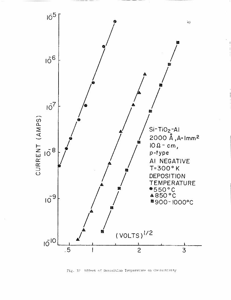
P - ~ Y P ~ A l NEGATIVE T = 3 0 0 ° K DEPOSITION TEMPERATURE '550°C ~ 8 5 0 ° C 9 0 0 - 1000°C
Fig. 12 Effect of Deposition Temperature on Conductivity
4 s to i ch iome t r i c Ti0 i n Chapter I V , have a cu r r en t dens i ty about 10 t imes
2
g r e a t e r t han t h e 900°C f i lms a t a given f i e l d s t r e n g t h . This g ives some fur -
t h e r evidence of a bulk conduction mechanism. The breakdown s t r e n g t h of
t h e s e 550°C f i lms i s only about 2 vol t ,s f o r a 2000 f i l m . The 850°C f i lms
e x h i b i t a conduct iv i ty an o rde r of magnitude g r e a t e r t han t h e 900°C f i lms
and a breakdown s t r e n g t h of about 5 v o l t s . The 900°C f i lms have a breakdown
s t r e n g t h of 10 v o l t s which corresponds t o a f i e l d s t r e n g t h of 5 x l o 5 vol ts /cm.
Films formed between 900°c t o 1000°C show s i m i l a r c h a r a c t e r i s t i c s , When t h e
550°C f i lms and t h e 850°C f i lms a re oxid ized f o r two hours i n dry 0 a t 800°C, 2
as descr ibed i n Chapter I V , t h e p r o p e r t i e s of t h e s e f i lms become equiva len t
t o t h e 900°C samples sugges t ing t h a t t h e oxygen anneal r ep l aces miss ing oxygen
and r e s t o r e s t h e f i l m t o s to i ch iome t r i c Ti0 2 '
Figure 11 shows t h a t at low f i e l d s when t h e work func t ion of t h e posi-
t i v e e l e c t r o d e i s h ighe r than t h a t of t h e negat ive one, Poole-Frenkel mechan-
ism i s e f f e c t i v e l y cu t o f f by t h e negat ive e l e c t r i c f i e l d a t app l i ed vol tages
l e s s than t h e d i f f e r e n c e i n b a r r i e r h e i g h t s , and e l e c t r o n hopping from one
s i t e t o another may occur . ~ e a d ~ ~ observes t h i s f o r Ta 0 f i l m s , and he ob- 2 5
se rves an ohmic c h a r a c t e r i s t i c a t very low f i e l d s , Mead f i n d s t h a t somehow
t h i s ohmic behavior occurs a t such low f i e l d s and low c u r r e n t s t h a t it i s d i f -
f i c u l t t o observe experimental ly . F igure 1 3 shows t h a t f o r n-type ma te r i a l
where t h e work funct ion of t he p o s i t i v e e l ec t rode i s lower t han tha t , of t he
nega t ive one, t h e Poole-Frenkel mechanism i s not cu t o f f by t h e f i e l d .
Equations 29 and 30 y i e l d m as t h e expected s lope of I n I v s , 5 112
i f Schot tky o r Poole-Frenkel mechanisms a r e p re sen t . The s lope should f a l l
between
- 3 < m < 1 . 4 6 x 0 . 7 3 ~ 1 0 - - ( m / ~ o l t )'I2 [36 1
u s ing a d i e l e c t r i c cons tan t of 4 ( squa re of t h e index of r e f r a c t i o n ) . The
5 1
/' @
10
10
(.j ' 0 .5 1.0 2.8 3.0
(VOLTS)
2000 a , A=lmm2
IO -crn n-type A l POSITIVE T = 3 0 0 ° K
Fig. 13 Current vs ( ~ o l t a ~ e ) " ~ for MIS Device

lower l i m i t app l i e s f o r Schottky emission (equat ion 1 2 ) and f o r Poole-
Frenkel emission wi th only one type of c a r r i e r p r e s e n t , The upper l i m i t ap-
p l i e s f o r Poole-Frenkel emission wi th compensation (both donor and acceptor
s i t e s ) . The value of m from f i g u r e 9 and f i g u r e 11 a r e t h e expected values
f o r Poole-Frenkel emission wi th compensation (11 .5 x The s lope would
be one-half t h i s f o r Schottky emission. The s lope of t h e curves of f i g u r e 1 2
( -2.4 x a r e about 50% l a r g e r than one would expect f o r Poole-Frenkel
emission, Severa l p o s s i b l e explana t ions a r i s e f o r t h i s : a ) P a r t of t h e f i e l d
appears across t h e t h i n SiO l a y e r under t h e Ti0 . b ) ~ e a d ~ ~ notes t h a t i n t h e 2 2 '
majo r i ty of h i s t h i c k e r f i lms some mechanism, poss ib ly concent ra t ion of t h e
f i e l d i n small regions o f t h e m a t e r i a l due t o a change i n t he s t r u c t u r e of
t h e f i l m , r a i s e d t h e experimental m ; c ) t he low a c t i v a t i o n energy (0.11 eV)
sugges t t h a t perhaps some e l e c t r o n hopping from one t r a p t o another wi th low
mob i l i t y i s occurr ing i n combination wi th t h e Poole-Frenkel mechanism93; d )
examination of t h e Poole-Frenkel e f f e e t express ion , equat ion 24 and 25, shows
t h a t f o r accu ra t e comparison, experimental values of I n (11~) should be
p l o t t e d versus v1I2. F igure 1 4 shows t h e r e s u l t o f t h i s f o r t h e 9 0 0 ' ~ sample
of f i g u r e 12. The experimental s l o p e i s lowered from 2.4 x t o about
1 . 9 x because of t h e moderate f i e l d s involved. The experimental s lope i s
now only s l i g h t l y h i g h e r t han t h e p r e d i c t e d va lue . For very high f i e l d s a s
many au thors use f o r S i N t h i s c o r r e c t i o n i s n e g l i g i b l y sma l l ; e ) although 3 4
t h e measurements p re sen ted he re a r e apparent ly s t eady- s t a t e va lues , a decay i n
c u r r e n t l a s t i n g from a few seconds t o a minute was observed a f t e r i nc reas ing
t h e vo l t age and i f space charge reg ions a s s o c i a t e d wi th t h e con tac t s p e r s i s t ,
t h e i r width w i l l decrease the e f f e c t i v e th i ckness of t h e f i lms causing t h e
34 s l o p e , m y t o be high . The b a r r i e r he igh t $J determined by t h e o r d i n a t e i n t e r c e p t of I n J
s
A l NEGATIVE,
T = 300°K
VOLTS I/%
Fig. 14 Conduct ivi ty v s . (Vol tage) 112

54 .
vs . <'I2 p l o t s (equat ion 13, 5 = 0 ) d i f f e r s from t h a t determined by t h e cur-
r e n t v a r i a t i o n wi th temperature (equat ions 24,25 and 2 6 ) . This i s f u r t h e r ev i -
dence t h a t Poole-Frenkel i s t h e dominant mechanism r a t h e r t han Schottky. The
value of t h i s low f i e l d a c t i v a t i o n energy ranges from 1 .08 eV f o r t h e high
r e s i s t i v i t y Ti0 samples t o approximately 0.83 eV f o r t h e more conductive sam- 2
p l e s when c a l c u l a t e d from i n J vs . $I2 , bu t it i s 0.25 eV when ca l cu la t ed
from I n J v s , l / T , Therefore , t h i s a c t i v a t i o n energy i s equal t o t h e energy
34 d i f f e r ence between t h e emission s i t e s and t h e band edge and i s equal t o ap-
proximately 0.2 5 eV.
These cons idera t ions i n d i c a t e t h a t t h e dominant conduction mechanism
i n t i t an ium dioxide i s Poole-Frenkel emission from donor and acceptor s i t e s
and t r a p s w i th in t h e bulk of t h e Ti02 f i lm . The s i t e s l i e approximately 0.25
eV from t h e band edge, Both donor and acceptor s i t e s a r e p re sen t c r e a t i n g a
compensating e f f e c t .
CHAPTER V 1 3
CAPACITANCE-VOLTAGE PROPERTIES OF METAL-Ti0 -SILICON 2
The MOS capac i to r s t r u c t u r e s ens i t3ve ly r e f l e c t s t h e e l e c t r i c a l prop-
e r t i e s gf t h e s i l i c o n - t i t a n ~ u m &-oxide system. A major discontinuity ex l sks
a t t h e i n t e r f a c e between t h e ordered semiconductor c r y s t a l l a t t i c e and t h e
oxide l a y e r , Energy s t a t e s appear I n t h e forbidden band of t h e i n t e r f a z e
where, a s l oca l i z , ed allowed energy l e v e l s , they become sources of charge
s t r o n g l y a f f e c t i n g t h e devi ces p r o p e r t i e s . Ca,pacitance measuremen's y i e l 4 ln-
C9*rnatlon c z n ~ e r n i n g t h e s e s t a t e s .
The l i 1;eratv.re contains extensive r e p o r t s on MOS wark us ing s l l i - o n
125 d-Fci dloxide and, move r e c e n t l y , s i l i c o n n ~ t ' r i d e a s t h e i n s u l a t o r , Terman
t h e f i r s t major work on t h e MOS s t r u c t u r e I n 1961 a t S tanford Unrverel ty In
8 c! 62 l a r e 196!, Llndner r epo r t ed on t h e MOS su? f i ce va rac to r . Lehovec8', Gro.re ,
56 8 8 Ga,rrett and B i a t t a i n , Marcus , Gray and and many o the r s hare made
s l gni f i c a n t con t r lbu t Ions toward unders t and3 ng MOS phenomena,
A, Theory of t,he MOS S t r u c t u r e .
Numer9us m t k o r s rt .port trhe d e t a l l e d mathematical. ana lys i s 01' t h e
theory of t h e MOS device,. This s e c t l o n gives a qualitative d2scu.ssisn of t h r s
r h e o q - Consrder t h e device of f i g u r e 15 us lng a p-type semicondu=to:- Blas
appl-i-at.zon consists of a dc p o t e n t i a l app l l cd t o t h s d e ~ r l c e w i t h a slAp?-.lrn-
posed ac component, The capaci tance br idge r equ i r e s t h e ac component i n t h e
measurement, The ac componenS i s l e s s than 10 m i l 1 i v o l t s . T h e potent, la? 1 s
?ailed a dc b i a s , however, *,he f a c t %hat an a r rapac7tan-e i s a c t u a l l y mea-
sured l s of g rea t importance li-l t h e high frequency case . Th-i f2l lowing d i s -
cussion i s for t h e I d e a l case with no su r f ace s t a t e s o r work f u n c t i ~ n e f i e r t s :
1 Accurnulat i on Reg1 on.
Conslder t h e s i t u a t i o n of t he metal b l a sed negat ive wi th r e spec t t o

semi conduct o r
- - -
met a 1 loxidl semiconductor / f
( a ) Accumulation (b ) Depletion ( c ) Invers ion
F ig . 15 Energy Bands and Charge Di s t r ibu t ion of MIS S t r u c t u r e
Neglecting Surf ace S t a t e s and Work Function Differences
t h e semiconductor, Figure 15a p r e s e n t s a band p i c t u r e r ep re sen t ing t h i s s i t -
ua t ion . The app l i ed f i e l d causes ma jo r i t y c a r r i e r s ( h o l e s ) t o d r i f t t o t h e
l e f t , bu t t h e i r flow i s blocked by t h e d i e l e c t r i c . As a r e s u l t , an accumula-
t i o n of major i ty c a r r i e r s forms a very narrow reg ion a t t h e s i l i con-oxide in-
t e r f a c e , The ac component of t h e b i a s vol tage modulates t h e d r i f t v e l o c i t y
of t h e s e c a r r i e r s , bu t t h i s modulation i s smal l . The capac i tance measured i s
t h a t of t h e oxide and i s given by
The charge i n t h e space charge region of t h e semiconductor i s equa l
and oppos i te t o t h e charge on t h e meta l p l a t e due t o t h e requirement of charge
conserva t ion . The capac i tance of t h e oxide i s independent of b i a s , I n view
of t h e forward b i a s , the only c a r r i e r s of i n t e r e s t i n t h i s reg ion a r e t h e ma-
j o r i t y c a r r i e r s . The mobi l i ty of t h e s e i s such t h a t a t a l l f requencies of i n -
t e r e s t they w i l l reach equ i l i b r ium throughout t h e semiconductor very qu ick ly ,
This s i t u a t i o n can be considered one of quasi equi l ibr ium.
2 F l a t Band Region.
The f l a t band case r e s u l t s a t zero b i a s . As t h e name i m p l i e s , t h e
bands a r e f l a t up t o t h e edge of t h e semicond-uctor with no bending f o r t h i s
cond i t i on ,
3. Deplet ion Regi on.
As t h e b i a s becomes p o s i t i v e , t h e band p i c t u r e appears s i m i l a r t o f i g -
ure 15b and a space charge reg ion appears i n t h e semiconductor, The space
charge c o n s i s t s of uncompensated acceptor i ons and t h e t o t a l charge i n t h e
space charge reg ion i s j u s t equa l and oppos i te t o t h e charge on t h e meta l
e l e c t r o d e . The capac i to r which i s being measured c o n s i s t s now of two d i e l ec -
t r i e s , t h e oxide and t h e dep le t ion zone of t h e semiconductor. The express ion
f o r t h e capaci tance of a capac i to r wi th t h i s con f igu ra t ion i s t h e same a s f o r
two p a r a l l e l p l a t e capac i to r s i n s e r i e s ,
where C i s given by equat ion 31 and 0
as t h e b i a s i s i nc reased t h e deple t ion width inc reases and C decreases .
4, Invers ion Region.
A t some p o s i t i v e b i a s poin t t h e p o t e n t i a l o f t h e s i l i con-oxide i n t e r -
f ace i s such t h a t t h e band i s bent s u f f i c i e n t l y t o f o r c e t h e Fermi l e v e l
above midgap ( t h e i n t r i n s i c l e v e l ) , causing t h e concent ra t ion of e l ec t rons
a t t h e i n t e r f a c e t o i n c r e a s e sha rp ly . This i s i n e f f e c t n-type m a t e r i a l and
f o r a sma l l , bu t f i n i t e , d i s t ance i n t o t h e semiconductor t h e major i ty car-
r i e r s a r e now e l e c t r o n s . This i s c a l l e d an inve r s ion l a y e r and i s shown i n
f i g u r e l 5 c , The n e t charge of e l ec t rons i n t h e inve r s ion l a y e r has t h e same
s i g n a s t h e uncompensated acceptor charge i n t h e space charge reg ion .
a , Low Frequency Case.
The low frequency invers ion l a y e r charge d i s t r i b u t i o n appears
i n f i g u r e 16a. A t l a r g e p o s i t i v e b i a s t h e charge i n t h e invers ion
l a y e r dominates and t h e capaci tance approaches t h a t of t h e accumula-
t i o n reg ion i f t he measurements a r e c a r r i e d out a t s u f f i c i e n t l y low
f requencies so t h a t minor i ty c a r r i e r s a r e genera ted f a s t enough t o
keep up wi th t h e small s i g n a l v a r i a t i o n . I n t h i s case t h e generated
holes w i l l r e p l e n i s h t h e holes p u l l e d out o f t h e edge of t h e deple-
t i o n region and t h e e x t r a e l ec t rons w i l l appear i n t h e invers ion l a y e r .
The capaci tance curve i s s i m i l a r t o curve "a" i n f i g u r e 16c f o r t h e
low frequency case because t h e incremental nega t ive charge w i l l

p-type semiconductor
X
Fig. 16 Charge Distribution and Capacitance Variation
for (a) Low Frequencies (b) High Frequencies
appear a t t h e oxide-s i l icon i n t e r f a c e .
b . High Frequency Case.
A t high frequencies s u f f i c i e n t minor i ty c a r r i e r s cannot be gen-
e r a t e d w i t h i n a cyc le of t h e ac s i g n a l , t h u s , t h e charge i n t h e in -
vers ion reg ion i s constant ( a s determined by t h e dc b i a s ) and has
no e f f e c t on t h e capaci tance readings . The only charge d i s t r i b u t i o n
i n t h i s case i s a t t h e bulk semiconductor end of t h e deple t ion re -
gion. Figure 16b i l l u s t r a t e s t h i s p o i n t . The dep le t ion width con-
t i n u e s t o i n c r e a s e with l a r g e p o s i t i v e b i a s a s ho les a r e p u l l e d ou t
of t h e semiconductor and t h e t o t a l capac i tance cont inues t o decrease .
When t h e width of t h e dep le t ion l a y e r no longer i nc reases w i th b i a s ,
t h e capac i tance value again becomes cons t an t . The capaci tance curve
i s s i m i l a r t o t h e curve "b" i n f i g u r e 16c .
5 . The E f f e c t of Surface S t a t e s .
Surface s t a t e s e x h i b i t energy l e v e l s w i th in t h e forbidden band of
t h e semiconductor. These a re a s soc i a t ed wi th t h e atoms on o r very near t h e
su r f ace of t h e s i l i c o n a t t h e s i l i con-oxide i n t e r f a c e . Tamm and Shockley 8 7
pred ic t ed t h e s e s t a t e s t h e o r e t i c a l l y because of a break i n t h e p e r i o d i c i t y of
t h e l a t t i c e a t t h e i n t e r f a c e . They r ep resen t a source ( o r s i n k ) o r charge
and t h e r e f o r e may a l t e r t h e e l e c t r i c f i e l d w i th in t h e device.
Not a l l of t h e su r f ace s t a t e s a r e f i l l e d ; t hose above t h e Fermi
l e v e l having a low occupation p r o b a b i l i t y and those below t h e Fermi l e v e l
having a high occupation p r o b a b i l i t y a s i n f i g u r e 17 . Ionized donor atoms a t
t h e i n t e r f a c e a r e a source of p o s i t i v e charge, while t h e f i l l e d donor s t a t e s
a r e n e u t r a l . Unionized acceptor atoms a r e n e u t r a l , and when ion ized acceptor
atoms represent a source of nega t ive charge a t t h e i n t e r f a c e . When a b i a s
s h i f t modulates t h e energy bands r e l a t i v e t o t h e Fermi l e v e l a change i n t o t a l

F i g . 1 7 S u r f a c e S t a t e Occupancy i n Regions o f
( a ) Flat-Band (b) Accumulation ( c ) I n v e r s i o n

charge p re sen t a t t h e i n t e r f a c e r evea l s t h e presence of t h e su r f ace s t a t e s .
As t h e su r f ace i s accumulated, t h e s t a t e s a r e l i f t e d f a r above t h e Fermi
l e v e l and t h e i r p r o b a b i l i t y of occupation by e l e c t r o n s i s smal l . As t h e
su r f ace i s deple ted and i n v e r t e d , t h e s t a t e s a r e p u l l e d way below t h e Fermi
l e v e l and t h e i r p r o b a b i l i t y of occupat ion i s h igh . Such s t a t e s whose
charge can be r e a d i l y exchanged wi th t h e semiconductor a r e c a l l e d f a s t
su r f ace s t a t e s . Since t h e charge i n t h e s e s t a t e s v a r i e s wi th t h e band bend-
i ng , t he capaci tance-vol tage c h a r a c t e r i s t i c s w i l l be d isp laced from t h e
t h e o r e t i c a l by an amount which i t s e l f v a r i e s wi th t h e su r f ace p o t e n t i a l .
This may appear as s t eps o r kinks o r a s a gradual d i s t o r t i o n of t h e cha rac t e r -
i s t i c s .
Some charges e x i s t i n t h e i n s u l a t o r which, although c lose t o t h e s i l -
icon i n t e r f a c e , cannot respond f a s t enough t o keep up with t h e band bending
caused by t h e modulation descr ibed above. These a r e c a l l e d oxide su r f ace
s t a t e s o r slow s t a t e s . To see how t h e s e a f f e c t t h e capaci tance-vol tage
curves, consider a charge shee t p e r u n i t a r e a Q w i th in t h e i n s u l a t o r a s
shown i n f i g u r e 18a . With zero ga t e vol tage t h i s charge w i l l induce an image
charge p a r t l y i n t h e meta l and p a r t l y i n t h e semiconductor. To obta in a
f la t -band condi t ion ( i . e . , no charge induced i n t h e semiconductor) , a nega-
t i v e vol tage must be appl ied t o t h e metal a s i n f i g u r e 18b. Increas ing
negat ive vo l t age p u t s more negat ive charge on t h e metal and thereby s h i f t s
the e l e c t r i c f i e l d d i s t r i b u t i o n downwards u n t i l t he e l e c t r i c f i e l d a t t h e
s i l i c o n s u r f a c e i s zero. The a r e a contained under t h e e l e c t r i c f i e l d d i s -
t r i b u t i o n i s t h e f la t -band vol tage , VFB. Using Poisson ' s equat ion , 'FB i s
given by
where x i s the d i s t ance from t h e metal t o t h e charge and d i s t h e d i s t a n c e
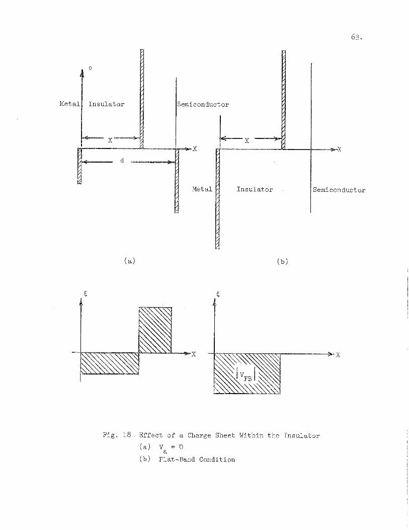
jemi conduct o r
Fig. 18 E f f e c t o f a Charge Shee t Within t h e I n s u l a t o r
(a) V = D a
(b) Flat-Band Condi t ion
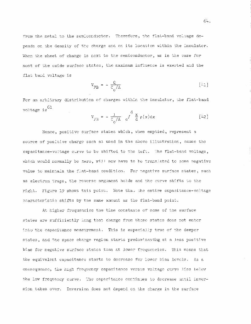
from t h e metal t o t h e semiconductor. Therefore, t h e f la t-band vol tage de-
pends on t h e dens i ty of t h e charge and on i t s l o c a t i o n wi th in t h e i n s u l a t o r .
When t h e shee t of charge i s next t o t h e semiconductor, as i n t h e case f o r
most of t h e oxide su r f ace s t a t e s , t h e maximum in f luence i s exer ted and t h e
f l a t band vol tage i s
For an a r b i t r a r y d i s t r i b u t i o n of charges w i th in t h e i n s u l a t o r , t h e f l a t -band
vol tage i s 61
- 1 VFB - - - x C /A o f g p(x )dx 0
Hence, p o s i t i v e su r f ace s t a t e s which, when emptied, r ep re sen t a
source of p o s i t i v e charge such as used i n t h e above i l l u s t r a t i o n , cause t h e
capaci tance-vol tage curve t o be s h i f t e d t o t h e l e f t . The f la t -band v o l t a g e ,
which would normally be zero , w i l l now have t o be t r a n s l a t e d t o some nega t ive
value t o maintain t h e f la t -band condi t ion . For nega t ive su r f ace s t a t e s , such
as e l e c t r o n t r a p s , t h e r eve r se argument holds and t h e curve s h i f t s t o t h e
r i g h t . Figure 19 shows t h i s p o i n t . Note t h a t t h e e n t i r e capaci tance-vol tage
c h a r a c t e r i s t i c s h i f t s by t h e same amount as tlie f la t -band po in t .
A t h ighe r frequencies t h e time cons tan ts of some of t h e su r f ace
s t a t e s a r e s u f f i c i e n t l y long t h a t charge from t h e s e s t a t e s does not e n t e r
i n t o t h e capaci tance measurement. This i s e s p e c i a l l y t r u e of t h e deeper
s t a t e s , and t h e space charge reg ion s t a r t s predominanting a t a l e s s p o s i t i v e
b i a s f o r nega t ive su r f ace s t a t e s than a t lower f requencies . This means t h a t
t h e equiva len t capaci tance s t a r t s t o decrease f o r lower b i a s l e v e l s . As a
consequence, t h e high frequency capaci tance versus vol tage curve l i e s below
t h e low frequency curve. The capaci tance cont inues t o decrease u n t i l inver-
s ion t a k e s over . Invers ion does not depend on t h e charge i n t h e su r f ace
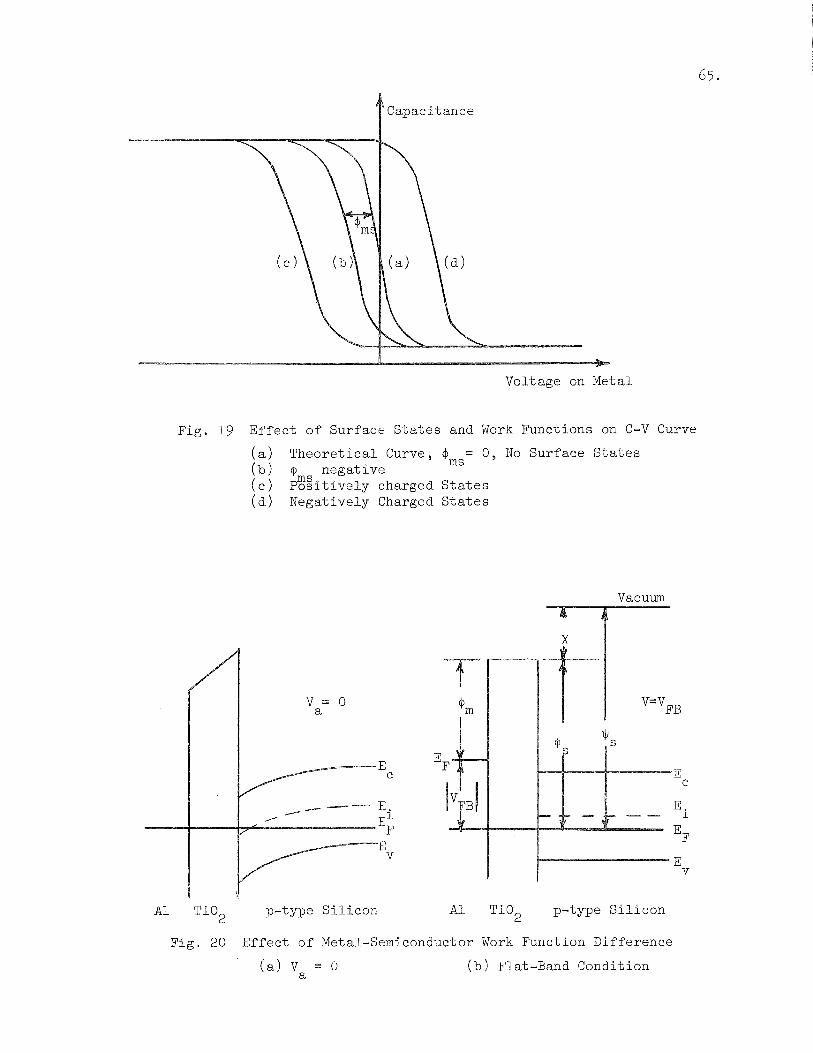
Voltage cn Metal
F ig . 1 9 Effec t of Surface S t a t e s and Work Functions on C-V Curve
( a ) Theore t i ca l Curve, 'ms = 0 , No Surface S t a t e s
(b) (ms nega t ive ( c ) P o s i t i v e l y charged S t a t e s ( d ) Negat ively Charged S t a t e s
Vacuum
A1 Ti02 p-type S i l i c o n A 1 Ti02 p-type S i l i c o n
Fig . 20 Ef fec t o f Metal-Semiconductor Work Function Difference
( a ) Va = 0 (b ) Flat-Band Condition
s t a t e s but only on t h e su r f ace p o t e n t i a l and, t h e r e f o r e , begins a t t h e same
value of b i a s as i n t h e low frequency case .
Grove6l p re sen t s a d d i t i o n a l information on su r f ace s t a t e s i n t h e Si-
87 SiO system. Many, Golds te in , and Grover present a more comprehensive 2
t rea tment of t he theory of semiconductor su r f aces .
6. E f f e c t of I n t e f a c e Contact P o l a r i z a t i o n P o t e n t i a l s .
Upon making c o n t a c t , t h e mutual i n t e r a c t i o n of two ma te r i a l s r e s u l t s
i n t h e formation of an i n t e r f a c i a l contac t p o l a r i z a t i o n p o t e n t i a l . This po-
t e n t i a l can a r i s e from a t r a n s f e r of e l e c t r o n s from su r face s t a t e s on one
m a t e r i a l t o su r f ace s t a t e s on t h e o t h e r o r from a perturba, t ion of t h e su r f ace
s t a t e s themselves. ~ c h m i d l i n l ' l cons iders t h e poss ib l e s h i f t o f energy bands
of t h e mating ma te r i a l s with r e spec t t o each o t h e r by an amount equal t o t h i s
p o l a r i z a t i o n p o t e n t i a l . Donating t h i s p o t e n t i a l drop by A t h e r e s u l t a n t a i '
i n t e r f a c i a l b a r r i e r he igh t C$ f o r t h e M I M s t r u c t u r e of f i g u r e 5 i s given by o a
- C$oa - +ma - x - Aai [431
where + i s t h e work func t ion of meta l a , and x i s t h e e l e c t r o n a f f i n i t y of ma
t h e d i e l e c t r i c . An analogous case e x i s t s f o r t h e s i l i con-Ti0 system of f i g - 2
ure 20 g iv ing an i n t e r f a c i a l b a r r i e r he igh t of
- OOS - '4Js - X - ASi
where t h e s u b s c r i p t "s t ' denotes t h e semiconductor.
Thus, an impuri ty at t h e i n t e r f a c e can be po la r i zed and t h e asso-
c i a t e d p o t e n t i a l s t e p becomes p a r t o f A causing a change i n t h e i n t e r f a c - s i ' i a l b a r r i e r h e i g h t .
7. E f f e c t of Work Function Dif fe rence .
The d i f f e r ence i n e l e c t r o n ene rg i e s a t t h e Fermi l e v e l i n t h e metal
and i n t h e semiconductor of an MOS s t r u c t u r e i s expressed as a d i f f e r e n c e
i n work func t ions , which i s t h e energy r equ i r ed t o move an e l e c t r o n from t h e
Fermi l e v e l i n a given m a t e r i a l t o vacuum. F igure 20a shows the e f f e c t of
b r ing ing t o g e t h e r an aluminum/titanium dioxide/^-type s i l i c o n s t r u c t u r e .
E lec t rons w i l l flow t o counterbalance t h e d i f f e r e n c e i n work func t ions un-
t i l the Fermi l e v e l i n t h e metal i s l i n e d up wi th t h e Fermi l e v e l i n t h e
semiconductor. Consider t h e condi t ion of f i g u r e 20b when j u s t enough g a t e
vol tage i s app l i ed t o counterbalance t h e work func t ion d i f f e r ence and a f l a t -
band condi t ion i s maintained i n t h e semiconductor. The g a t e vol tage r equ i r ed
t o b r i n g about t h e f la t -band condi t ion i s t h e f la t -band vol tage V FB ' Figure
20b g ives t h i s f la t -band vol tage as
B. Experimental Resul t s and Discussion.
This s e c t i o n d i scusses t h e experimental r e s u l t s ob ta ined from t h e
capaci tance-vol tage d a t a . The d a t a y i e l d d i e l e c t r i c cons tan ts , s u r f ace
charge and su r f ace s t a t e dens i ty numbers. Frequency e f f e c t s due t o va r ious
source m a t e r i a l s and C-V s h i f t s due t o va r ious e l e c t r o d e m a t e r i a l s a r e d i s -
cussed.
1. D i e l e c t r i c Constant.
The d i e l e c t r i c cons tan t of t i t a n i u m dioxide f i lms prepared on @ti-
num as descr ibed i n Chapter I V i s 80. This agrees wi th t h e va lue r epo r t ed
by ~ e u e r s a n g e r ~ ' f o r f i lms prepared a t low temperatures . The d i e l e c t r i c con-
s t a n t of f i lms depos i ted on s i l i c o n i s 50 as obta ined by measuring t h e capaci-
t ance a t 1 kHz o f an MIS s t r u c t u r e under b i a s condi t ions corresponding t o
s t r o n g accumulation of t h e s i l i c o n su r f ace . Using t h e approximation of
2000 1 of Ti02 ( K = 80) i n s e r i e s wi th d of SiO ( K = 4), one ob ta ins d = 2
60 1 f o r t h e th i ckness of t h e S i02 . This i s reasonable s i n c e some SiO would 2
form i n t h e atmosphere and t h e growth process t akes p l ace i n an ox id i z ing
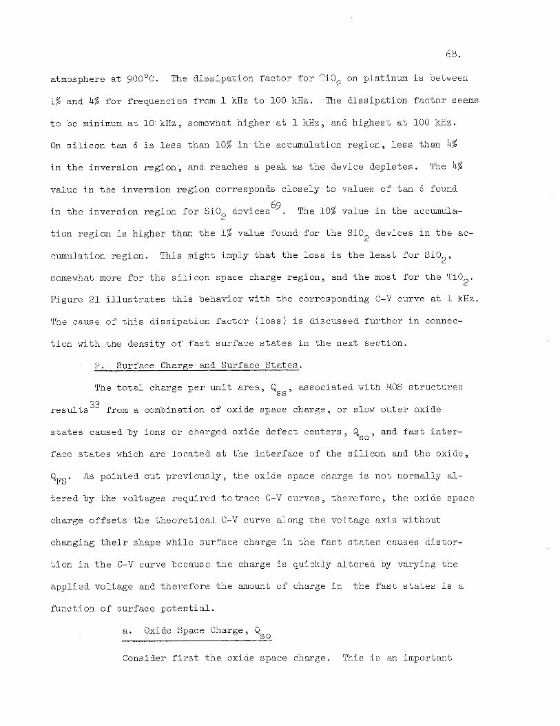
atmosphere a t 900°C. The d i s s i p a t i o n f a c t o r f o r Ti0 on plat inum i s between 2
1% and 4% f o r f requencies from 1 kHz t o 100 kHz. The d i s s i p a t i o n f a c t o r seems
t o be minimum a t 10 kHz, somewhat h ighe r a t 1 kHz, and h ighes t a t 100 kHz.
On s i l i c o n t a n 6 i s l e s s t han 10% i n t h e accumulation r eg ion , l e s s than 4%
i n t h e inve r s ion r eg ion , and reaches a peak a s t h e device d e p l e t e s . The 4%
value i n t h e invers ion reg ion corresponds c l o s e l y t o values o f t a n 6 found
i n t h e invers ion region f o r SiO devices69. The 10% value i n t h e accumula- 2
t i o n reg ion i s h igher than t h e 1% value found f o r t h e SiO devices i n t h e ac- 2
cumulation reg ion . This might imply t h a t t h e l o s s i s t h e l e a s t f o r S i02 ,
somewhat more f o r t h e s i l i c o n space charge r eg ion , and t h e most f o r t h e Ti02.
Figure 2 1 i l l u s t r a t e s t h i s behavior wi th t h e corresponding C-V curve a t 1 kHz.
The cause of t h i s d i s s i p a t i o n f a c t o r ( l o s s ) i s d i scussed f u r t h e r i n connec-
t i o n wi th the dens i ty of f a s t s u r f a c e s t a t e s i n t h e next s e c t i o n .
2. Surface Charge and Surface S t a t e s .
The t o t a l charge p e r u n i t a r e a , QSS , as soc ia t ed wi th MOS s t r u c t u r e s
r e s u l t s 3 3 from a combination of oxide space charge, o r slow o u t e r oxide
s t a t e s caused by ions o r charged oxide de fec t c e n t e r s , &SO , and f a s t i n t e r -
f ace s t a t e s which a r e l o c a t e d a t t h e i n t e r f a c e of t h e s i l i c o n and t h e oxide ,
QFS. A s po in ted out p rev ious ly , t h e oxfde space charge i s no t normally a l -
t e r e d by t h e v o l t ages r equ i r ed t o t race C-V curves , t h e r e f o r e , t h e oxide space
charge o f f s e t s t h e t h e o r e t i c a l C-V curve along t h e vol tage a x i s without
changing t h e i r shape whi le su r f ace charge i n t h e f a s t s t a t e s causes d i s t o r -
t i o n i n t h e C-V curve because t h e charge i s qu ick ly a l t e r e d by varying t h e
app l i ed vol tage and t h e r e f o r e t h e amount of charge i n t h e f a s t s t a t e s i s a
func t ion of su r f ace p o t e n t i a l .
a . Oxide Space Charge, Qs 0
Consider f i r s t t h e oxide space charge. This i s an important
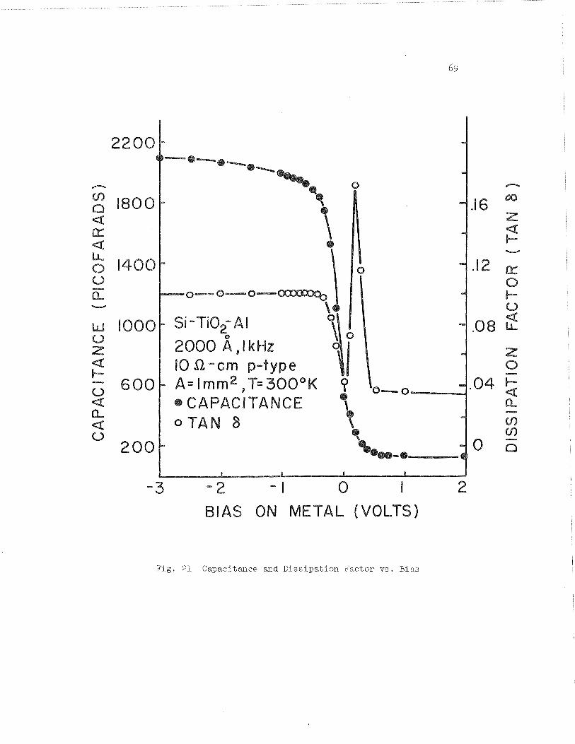
BIAS ON M E T A L (VOLTS)
Fig . 2 1 Capacitance and Di s s ipa t i on Fac tor v s . Bias
70
MOS parameter because it i s one of t h e parameters which c o n t r o l s t he thresh-
o l d of MOS enhancement mode FET* swi tches , t h e ope ra t ing p o i n t of MOS deple-
t i o n mode FET* a m p l i f i e r s , and t h e PNP t r a n s i s t o r c o l l e c t o r junc t ion leak-
age and p a r a s i t i c s u r f a c e capac i tances . The capaci tance-vol tage charac te r -
6 I. i s t i c s of MIS s t r u c t u r e s y i e l d information about t h i s charge . From equa-
t i o n 45, one determines t h e f la t -band vo l t age , VFB, of t h e measured C-V curve.
Using equat ion 4 1 t h e oxide space charge i s then given by
Figure 22 shows a t y p i c a l C-V p l o t f o r p-type s i l i c o n . The accumula-
2 t i o n capaci tance g ives C /A = 0.2lyF/cm . Determination of t h e f la t-band
0
5 3 vo l t age r equ i r e s c a l c u l a t i o n of t h e f la t-band capac i tance . From Frank1 ,
t h e su r f ace charge dens i ty i s
where
F(uS, 40) = + fi [(-L+, - u ) s inh % + cosh u - cosh -L+,] 112 S s
*An enhancement mode MOSFET i s a common type metal-oxide-semi conductor f i e l d -
e f f e c t - t r a n s i s t o r where t h e source - to-drain conduction i s dependent upon a
channel which i s e l e c t r o s t a t i c a l l y induced by t h e g a t e p o t e n t i a l . I n a de-
p l e t i o n mode MOSFET a sha l low, e l ec t r i ca l ly -conduc t ive channel connecting t h e
source and d ra in i s d i f f u s e d i n t o t h e device during f a b r i c a t i o n . This chan-
n e l , of t h e same conduct iv i ty t y p e as t he source and d r a i n , can be made more
r e s i s t i v e by vol tage-biasing t h e g a t e . In both of t h e s e dev ices , t h e output
cu r r en t i s c o n t r o l l e d by an e l e c t r i c f i e l d .
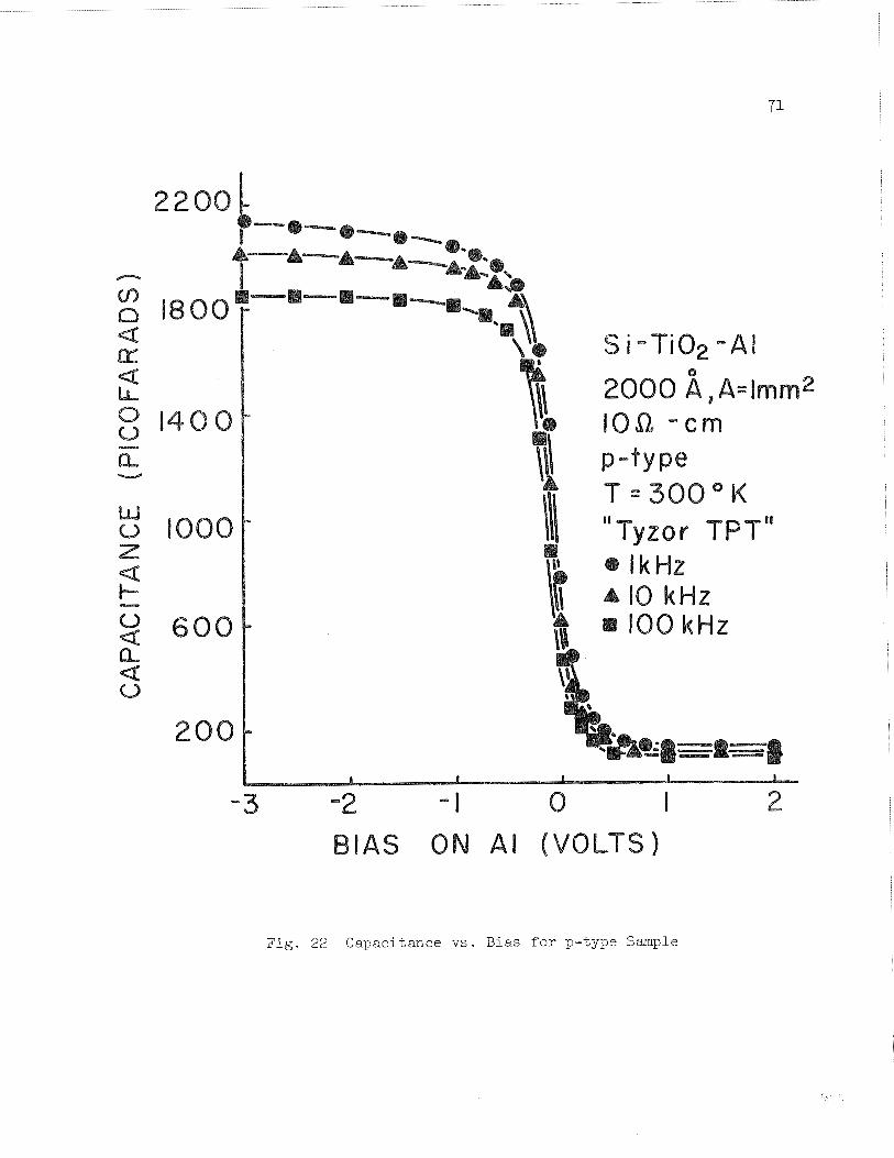
- .0 kHz m 100 kHz
\# d
Fig . 22 Capacitance vs. B i a s f o r p-type Sample

u,, and where where t h e ( - i s f o r u > y, and t h e (+ ) i s f o r u < s
where b denotes bu lk , s denotes su r f ace and L i s t h e i n t r i n s i c sc reening D
l e n g t h , ( Debye ~ e n ~ t h )
The capac i tance p e r u n i t a r e a of t h e space charge l a y e r i s
K E s i n h u .- s i n h yo S 0 - - - s
L~ F (us , y,) The f la t -band condi t ion occurs when u
S = u,, and
112 = K & ( C O S ~ u ~ ) /LD = I ( S ~ O / L B 'SFB s 0
which g ives f o r p-type m a t e r i a l with N ca r r i e r s / cm 3 A
-16 C s F B = 7 . 4 x 1 0 ( ~ o o K ~ N ~ / T ) ~ ' ~ farads/cm 2
For 10Q-cm p-type s i l i c o n , N = 1 .35 x 10 A 15cmq3, which g ives CSFB=O. 095
The MOS f la t -band capac i tance is then n n L L
- - o SFB 'FB co+ cSFB
Using t h e above values f o r C and C g ives C = 645 pF. Then, from f i g u r e o SFB FB
22, t h i s capaci tance y i e l d s t h e f la t -band v o l t age, VFB = 0 .
73.
Determination of Q now r e q u i r e s t h e metal-semiconductor work func- S 0
t i o n d i f f e r e n c e , %IS , from
6 1 From Grove , f o r aluminum and 10R-cm p-type s i l i c o n 4 = - 1 .05 .
ms 2
These values and equat ion 46 y i e l d Qso = 2 .2 x coulombs/cm o r a den-
2 s i t y of s t a t e s N = 1 . 3 8 r 10'' s t a t e s / cm . Figure 23 shows a t y p i c a l C-V
s 0
p l o t us ing n-type, IOR-cm s i l i c o n . I n t h i s ca se , 'FB
= 0.57 v o l t and 4ms =
- 0.53 v o l t . This y i e l d s Qso = 2 . 3 x low7 coulombs/cm2 and N = 1 . 4 5 x 10 12
s 0
2 s t a t e s l c m . Note from t h e d i r e c t i o n of t he C-V s h i f t t h a t t h e s e a r e nega t ive
su r f ace charges ( f i g u r e 19\. For t h e p-type s i l i c o n , t h e work func t ion d i f -
fe rence t r i e s t o s h i f t t h e curve t o t h e l e f t , but t h e negat ive s u r f a c e
charges t r y t o s h i f t t h e curve t o t h e r i g h t . The r e s u l t , f o r t h i s p a r t i c u l a r
c a s e , i s t h a t t h e s e two e f f e c t s exac t ly compensate each o t h e r and t h e f l a t -
band vol tage remains a t zero . For t h e n-type m a t e r i a l , t h e work func t ion d i f -
fe rence i s l e s s t han above and t h e negat ive su r f ace s t a t e dens i ty i s about t h e
same, wi th t h e n e t r e s u l t being a s h i f t i n t h e f la t -band vol tage t o t h e r i g h t .
The n-type s i l i c o n seems t o have more negat ive su r f ace charges t han t h e p-
t y p e which would be expected q u a l i t a t i v e l y s ince a h igher Fermi l e v e l would
allow more nega t ive s t a t e s t o e x i s t below t h e Fermi l e v e l , and t h e n-type
m a t e r i a l has a h ighe r Fermi l e v e l t han p-type m a t e r i a l .
b , Fast I n t e r f a c e Surface S t a t e s , QFS
Consider now t h e f a s t su r f ace s t a t e s . Fas t i n t e r f a c e s t a t e
l e v e l s a l t e r t h e performance of MOS devices by a l t e r i n g t h e reac tance of
t h e MOS v a r a c t o r by f i l l i n g and emptying i n and out of t h e s e s t a t e s a t t h e
a c measuring frequency and t h e charge i n t h e s e s t a t e s i s an added component
t o t h e su r f ace charge a t t h e insulator-semiconductor i n t e r f a c e . These f a s t
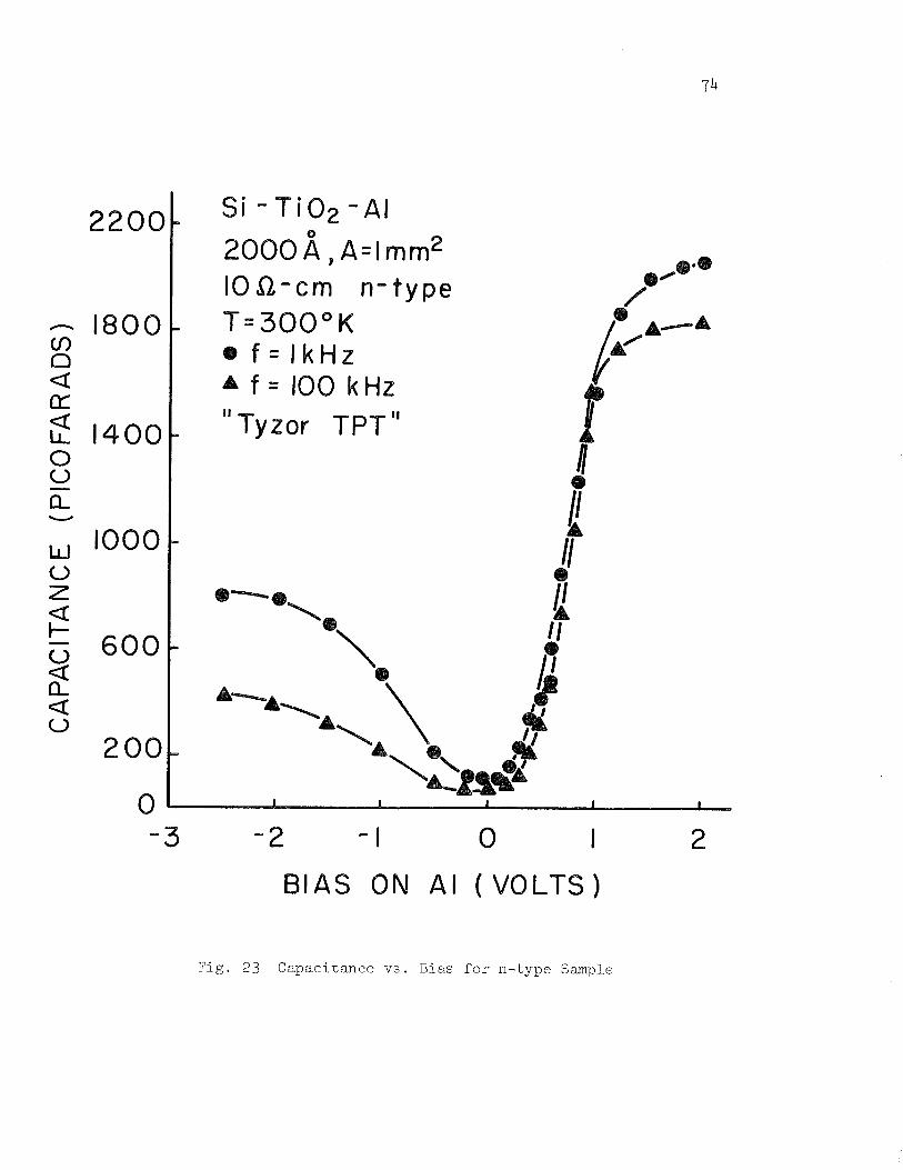
2 2 0 0
I O n - c m n- type - 1800 Cn (3 a CZT:
A f = 1 0 0 kHz
1400 0 0 - n - W 1000 0 Z a t- - 600 3 n a 0
200
0 - 3 -2 - I 0 I 2
BIAS ON A I (VOLTS)
F i g . 23 Capac i t ance vs . Bias f o r n- type Sample
s t a t e s can inc rease t h e switching vol tage of enhancement mode f i e l d e f f e c t
t r a n s i s t o r s and decrease t h e channel mobfl i ty causing lower gain-bandwidth
products i n MOSFET's.
Fas t i n t e r f a c e su r f ace s t a t e s cause d i s t o r t i o n i n t h e C-V curve.
The experimental C-V curves fol low t h e shape of t h e t h e o r e t i c a l curve
c l o s e l y , implying t h a t t h e dens i ty of f a s t s t a t e s i s - n o t t oo high. Grove 6 1
says t h a t a high degree of p a r a l l e l i s m of experimental c h a r a c t e r i s t i c s i n d i -
c a t e s t h a t t h e t o t a l dens i ty of su r f ace s t a t e s i n t h e middle 0 . 7 eV p o r t i o n
6 1 of t h e s i l i c o n energy band i s l e s s than 5 x 10" c c 2 . Grove says a l s o
t h a t only those s t a t e s which a r e w i th in a few kT i n energy of t he middle of
t h e energy gap con t r ibu te e f f e c t i v e l y t o su r f ace recombination and genera-
t i o n and hence t h e C-V c h a r a c t e r i s t i c s w i l l not be a f f e c t e d much by s t a t e s
n e a r t h e band edges. There a r e t h r e e techniques f o r measuring t h e s e f a s t
s t a t e s . The method of Nicol l ian and Goetzberger 100'101 g ives t h e dens i ty of
s t a t e s i n t h e cen te r h a l f of t h e band us ing MOS su r face conductance measure-
ments. The method of ~ e r m a n ' ~ ~ uses t h e capaci tance d i spe r s ion technique .
60 The method of Gray and Brown g ives t h e dens i ty of s t a t e s i n t h e top q u a r t e r
and bottom q u a r t e r of t h e band by scanning t h e forbidden gap us ing C-V mea-
surements wi th temperature. The method of measurement f o r t h e Gray and Brown
technique i s t h a t of determining t h e change i n vol tage and hence t h e change
i n su r f ace charge r equ i r ed toma in ta in t h e f la t -band condi t ion a s t h e Fermi
l e v e l w i th in t h e s i l i c o n i s v a r i e d by changing t h e sample 's temperature from
300°K t o 100°K. Performing t h e measurements a t 100 kHz in su res t h a t any
charge i n t h e i n t e r f a c e s t a t e s does not con t r ibu te apprec iab ly t o t h e ac ca-
pac i tance so t h e measured ac capac i ty i s almost e n t i r e l y due t o f r e e c a r r i e r s .
For t h e p-type samples, it requ i r e s l e s s p o s i t i v e o r more negat ive
vo l t age on t h e metal e l ec t rode t o reach t h e f la t -band condi t ion a s t h e tem-
p e r a t u r e decreases . The reason f o r t h i s i s t h a t t h e Fermi l e v e l moves c l o s e r

t o t h e valence band- in a p-type materf a l - as t h e temperature decreases . A t
h igher tempera tures , t h e Fermi l e v e l i s above some i n t e r f a c e s t a t e s . These
a r e f i l l e d wi th e l e c t r o n s and a r e n e u t r a l . It t akes a p o s i t i v e ga t e vol tage
t o deple te p a r t i a l l y t h e hole concent ra t ion a t - t h e su r f ace . When t h e tern-
pe ra tu re decreases , t h e Fermi l e v e l moves c l o s e r t o t h e valence band and
some of t h e i n t e r f a c e s t a t e s ' l o s e e l e c t r o n s and-become p o s i t i v e l y charged.
I n t h i s i n s t a n c e , t h e i n t e r f a c e s t a t e s c o n t r o l t h e su r f ace p o t e n t i a l , and it
requ i r e s a l a r g e nega t ive g a t e vol tage t o - d e p l e t e t h e i n t e r f a c e s t a t e s of t h e i r
e l e c t r o n s i n o r d e r - t o reach the - f l a t -band condi t ion .
Changes i n t h e f la t -band vol tage a s t h e temperature i s changed g ive
t h e change-in i n t e r f a c e - s t a t e - c h a r g e d i r e c t l y s i n c e t h e r e i s no band bending
f o r t h i s condi t ion . I n t h e f la t-band cond i t i on , t h e su r f ace p o t e n t i a l i s
equal t o t h e bulk Fermi l e v e l which i s given by Grove6'. The procedure i s
t o vary t h e temperature while maintaining t h e f la t -band capac i ty , which i s
a l s o temperature dependent and i s ca l cu lab le from equat ion 56 a t var ious tem-
pe ra tu re s , by cont inuously a d j u s t i n g t h e b i a s . Figure 24 i l l u s t r a t e s t h e re -
s u l t s of t h i s measurement. This l i n e r ep re sen t s t h e su r f ace charge, QFS, a s
a func t ion of t h e s u r f a c e p o t e n t i a l 4 which i s equal t o t he Fermi l e v e l . s ' The dens i ty of s t a t e s , NFS, i s given by aQFS . These r e s u l t s show t h a t t h e
a % dens i ty of f a s t s t a t e s i s r e l a t i v e l y constant over t he range of measurement
2 and i s approximately 8 .5 x 10" s tateslev-cm .
Consider'now the method of Nicol l ian and Goetzberger 100,101 . BY
t h i s method, a measure o f t h e MOS va rac to r impedance g ives t h e i n t e r f a c e
s t a t e d e n s i t y , WFS , near t h e middle of t h e gap. Both t h e capaci tance and
equiva len t p a r a l l e l - conductance as ' func t ions o f vo l t age and frequency con-
t a i n i d e n t i c a l information about t h e i n t e r f a c e s t a t e s . Figure 21 shows t h a t
t h e conductance technique i s p o t e n t i a l l y more a c c u r a t e , because of t h e sharp
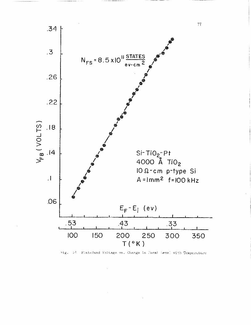
Si- Ti0,- P t
104-cm p-type Si A =lmm2 f=100 kHz
Fig. 24 Flat-Band Vol tage vs. Change in Fermi Level with Temperature
peak exh ib i t ed by t h e conductance ( d i r e c t l y r e l a t e d t o t h e d i s s i p a t i o n f a c t o r ,
t a n 6 ) , than t h e capaci tance technique .
The l o s s a r i s e s i n t h e fol lowing manner: When t h e ac s i g n a l moves
t h e conduction band toward t h e Fermi l e v e l i n t h e f i r s t ha l f of t h e c y c l e ,
t h e average energy of t h e e l ec t rons i n t h e s i l i c o n i s increased . Because a
conductance i s observed, it i s ev ident t h a t t h e i n t e r f a c e s t a t e s do not re-
spond immediately, bu t l a g behind. Therefore, e l e c t r o n s a t a h igher average
energy i n t h e s i l i c o n a r e captured by i n t e r f a c e s t a t e s a t a lower average
energy. This process r e s u l t s i n an energy l o s s . On t h e o the r h a l f of t h e
cyc le when t h e a c s i g n a l moves t h e valence band toward t h e Fermi l e v e l , t h e
e l e c t r o n s i n f i l l e d i n t e r f a c e s t a t e s have h igher -average energy than t h e
e l ec t rons i n t h e s i l i c o n . As t h e e l e c t r o n s a r e emi t t ed by t h e i n t e r f a c e
s t a t e s i n t o t h e s i l i c o n , they l o s e energy aga in . Therefore, t h e r e i s an
ene rgy - los s on both halves of t h e cyc le . The energy requi red f o r t r a n s i t i o n s
between t h e band edge and an i n t e r f a c e s t a t e i s muchhigher than t h i s and i s
suppl ied by phonons. The dominant l o s s mechanism i s t h e capture and emission
of major i ty c a r r i e r s . The i n t e r f a c e s t a t e s s t o r e charge and the re fo re have
a capaci tance C a s soc i a t ed with them which i s p ropor t iona l t o t h e i r d e n s i t y . S
The i n t e r f a c e s t a t e s reach equi l ibr ium wi th t h e s i l i c o n exponent ia l ly wi th
t ime T . The conductance r e l a t e d t o t h e l o s s i s G = C s / ~ . Therefore, mea- s
surement of equ iva l en t p a r a l l e l conductance y i e l d s t h e i n t e r f a c e s t a t e T and
The equ iva l en t c i r c u i t of f i g u r e 25 i l l u s t r a t e s t h e o r i g i n of t h e
l o s s ( t a n 6 ) . The d i s s i p a t i o n f a c t o r i s def ined a s
1 1 energy l o s s pe r cycle t a n 6 = - = - Q ~ T I maximum energy s t o r e d
The equiva len t impedance, z , of t h i s c i r c u i t i s

z = Real P a r t + Imaginary P a r t
2 Energy d i s s i p a t e d = 112 I [ ~ e a l P a r t o f z ] m
and
C Energy s t o r e d = 112 I [imaginary P a r t o f z ] m
hence from equat ion 58
This equat ion i s of t h e form
Aw t a n 6 = -
B+ Cw 2
where A , B , and C a r e cons tan ts
This same r e s u l t i s ob ta ined by cons ider ing t h e Debye equat ions f o r
a d i e l e c t r i c i n which t h e p o l a r i z a t i o n can r e l a x exponent ia l ly wi th charac-
t e r i s t i c t ime T a f t e r a change i n appl ied e l e c t r i c f i e l d occurs . The complex
d i e l e c t r i c constant may be w r i t t e n
where
y i e l d i n g
The equiva len t c i r c u i t of f i g u r e 25 i l l u s t r a t e s t h e p r i n c i p l e of t h e
MIS conductance technique .
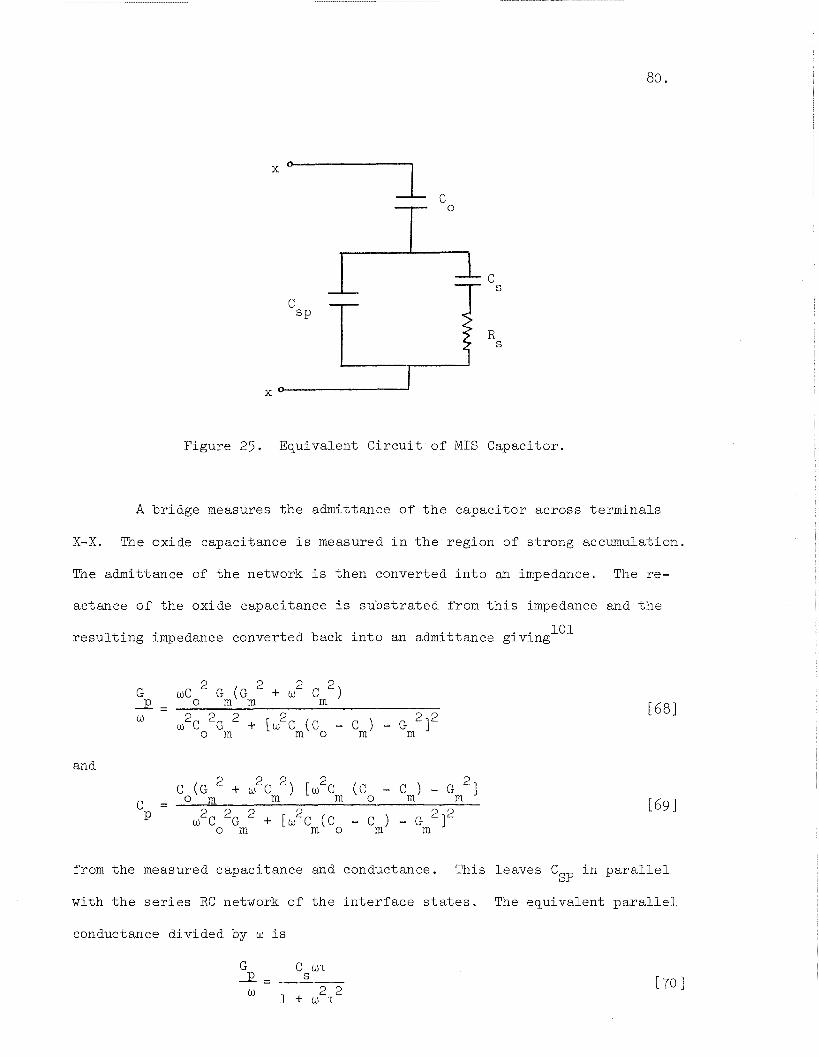
Figure 25. Equivalent C i r c u i t o f MIS Capaci tor .
A b r idge measures t h e admittance of t h e capac i to r across t e rmina l s
X-X. The oxide capaci tance i s measured i n t h e reg ion of s t rong accumulation.
The admittance of t h e network i s then converted i n t o an impedance. The re-
actance of t h e oxide capaci tance i s s u b s t r a t e d from t h i s impedance and t h e
r e s u l t i n g impedance converted back i n t o an admittance g iv ing 101
and
from t h e measured capac i tance and conductance. This leaves C i n p a r a l l e l SP
with t h e s e r i e s RC network of t h e i n t e r f a c e s t a t e s . The equivalent p a r a l l e l
conductance d iv ided by w i s

This equat ion depends only on t h e i n t e r f a c e s t a t e branch of t h e
equiva len t c i r c u i t . G / w goes through a maximum when w~ = 1. The va lue of P
G / w a t t h e maximum i s C /2 . Therefore, C i s c a l c u l a t e d from t h e peak of P S S
G / w which y i e l d s NFS. From f i g u r e 22 a t t h e peak of t a n 6 , Cm = 300 pF, P
t a n 6 = D = 0.17. The d i s s i p a t i o n f a c t o r r e l a t e s t o t h e conductance by m
This y i e l d s Gm = 0.32 umhos. C = 2000 pF. These values y i e l d N = 1 . 2 5 x o FS
1011 stateslev-em2. This value i s about on order of magnitude l e s s t han t h e
6 o value obta ined from t h e method& Gray and Brown . This i s expected, how-
e v e r , s ince both Gray6' and PJicoliian'O' p r e d i c t t h a t t h e dens i ty of s t a t e s
reaches a minimum very c l o s e t o midband and Grove61 s t a t e s t h a t t h e r e
should be l e s s than 1011 s t a t e s / e ~ - c m 2 i n order t o maintain p a r a l l e l i s m be-
tween t h e t h e o r e t i c a l and experimental curves.
The o t h e r method of c a l c u l a t i n g N involves t h e capaci tance d isper - FS
s i o n method of ~ e r m a n l ~ ~ . From t h e equiva len t c i r c u i t of f i g u r e 2 5 , t h e
equiva len t p a r a l l e l capaci tance i s
r-
where C i s given by equat ion 69. To e x t r a c t C from C us ing equat ion 72, P S P
C must be known. C can be ca l cu la t ed us ing an es t imated doping dens i ty s P s P
t o f i n d X and equat ion 39. However, t h e doping dens i ty i s not accu ra t e ly d
known near t h e s i l i c o n su r f ace because of p i l e up o r dep le t ion of t h e dopant
dur ing t h e growth of t h e i n s u l a t o r . However, t h i s discrepancy should not
be a s g r e a t f o r Ti0 a s f o r SiO because of t h e lower temperatures and 2 2
s h o r t e r t imes involved. The major d i f f i c u l t y a r i s e s from t h e f a c t t h a t t h e
i n t e r f a c e s t a t e capac i tance must be e x t r a c t e d from measured capac i tance
which c o n s i s t s of oxide capac i tance , deple t ion l a y e r capac i tance , and
i n t e r f a c e s t a t e capac i tance . Using t h e same parameters a s above, equat ion
72 gives C = 490 pF and NFS = 3.06 x 10¹¹ stateslev-em2. This va lue i s S
only about a f a c t o r of two d i f f e r e n t from t h a t ob ta ined by t h e Nico l l i an
method . The major conclusions drawn by Nico l l i an and ~ o e t z b e r ~ e r l ' l about
t h e i n t e r f a c e fol low.
( i ) A continuum of s t a t e s c l o s e l y spaced i n energy e x i s t s
ac ros s t h e energy gap.
( i i) The dominant con t r ibu t ion t o t h e conductance a r i s e s from
ma jo r i ty c a r r i e r t r a n s i t i o n s t o and from i n t e r f a c e s t a t e s . Thus,
t h e conductance a r i s e s s o l e l y from t h e s t eady- s t a t e l o s s due t o cap-
t u r e and emission of c a r r i e r s by i n t e r f a c e s t a t e s and not s t a t e s i n
t h e s i l i c o n space charge reg ion .
(iii) The f l u c t u a t i n g su r f ace p o t e n t i a l causes a d i spe r s ion o f
i n t e r f a c e s t a t e t ime cons tan ts i n t h e dep le t ion reg ion . This f l uc -
t u a t i o n can a r i s e from var ious sou rces , bu t i s p r imar i ly due t o a
random d i s t r i b u t i o n of su r f ace charge.
( i v ) I n t h e weak invers ion region t h e d i spe r s ion i s e l imina ted
by i n t e r a c t i o n between i n t e r f a c e s t a t e s and t h e minori ty c a r r i e r
band r e s u l t i n g i n a s i n g l e time cons tan t due t o t h e f a s t response
t ime of t he minori ty c a r r i e r s .
( v ) Capture c ros s s ec t ions f o r e l e c t r o n s and holes a r e inde-
pendent of energy over l a r g e po r t ions of t h e s i l i c o n bandgap.
( v i ) For a continuum of s t a t e s , t h e peak i n conductance oc-
curs when t h e response time of t h e i n t e r f a c e s t a t e s , which i s being
v a r i e d by t h e b i a s , equals t h e pe r iod of t h e appl ied s i g n a l f r e -
quency m u l t i p l i e d by a cons tan t . When generation-recombination
through i n t e r f a c e s t a t e s dominates t h e l o s s , t he conductance goes
through a peak a s a func t ion of b i a s i n weak inve r s ion because t h e
time cons tan t v a r i e s i nve r se ly wi th major i ty c a r r i e r dens i ty at t h e
sur face . If generation-recombination through bulk s t a t e s dominates
t h e l o s s , t h i s peak w i l l not occur . When t h e frequency i s i n c r e a s e d ,
t h i s peak s h i f t s t o a b i a s value corresponding t o a s u r f a c e p o t e n t i a l
nea re r t o f la t -band . For t h e C-V curve of f i g u r e 22, t h e peaks i n
d i s s i p a t i o n f a c t o r occur a t + 0 . 2 , + 0 . 1 and 0 f o r 1 kHz, 10 kHz and
100 kHz, r e s p e c t i v e l y , i l l u s t r a t i n g t h i s p o i n t .
3 6 Frequency E f f e c t s . A d i f f e rence between t h e TPT and PB prepared samples occurs i n t h e
frequency e f f e c t s . Figure 22 and f igu re 26 i l l u s t r a t e t h a t on p-type s i l i -
con t h e TPT samples e x h i b i t t h e high frequency c h a r a c t e r i s t i c i n t h e inver -
s i o n region between 1 kHz and 100 kHz, while t h e PB samples e x h i b i t t h e low-
e r frequency c h a r a c t e r i s t i c ; i . e . , t h e capac i tance r i s e s toward t h e oxide
value a s t h e frequency decreases from LOO kHz t o 1 kHz due t o a h ighe r gen-
6 1 eration-recombination r a t e . This d i f f e r ence occurs because t h e PB i s a
p a r t i a l l y hydrolyzed organometal l ie and conta ins an excess of water mole-
cu l e s . The presence o f excess water vapor has been shown t o a f f e c t MOS C-V
curves69. Figure 23 i l l u s t r a t e s t h a t t h e TPT formed n-type samples e x h i b i t
a frequency c h a r a c t e r i s t i c somewhere between t h e two cases above. The high
frequency case r e s u l t s because t h e measurement frequency i s much g r e a t e r
than t h e generation-recombination r a t e s o t h a t a l l t h e charge appears a t
t h e edge of t h e dep le t ion reg ion . I f t h e frequency i s low enough f o r gen-
erat ion-recombinat ion t o keep up wi th t h e small s i g n a l v a r i a t i o n , t h e gen-
eration-recombination mechanism l eads t o charge exchange with t h e inve r s ion

e- A = l mm2, T = 3 0 0 ° K .'e " Tyzor PB"
A\ @\ e I ~ H Z 10 kHz
.100kHz
BIAS ON Al (VOLTS)
F i g . 26 Capac i t ance vs . B i a s f o r "PB" Prepared Sample

l a y e r i n s t e p with t h e measurement s i g n a l and C w i l l approach C . The in - 0
vers ion s i d e of t h e C-V curves can a l s o be a f f e c t e d by su r f ace charge m i -
YY g r a t i o n over t h e oxide around t h e f i e l d p l a t e . Another frequency s e n s i t i v e e f f e c t occurs i n t h e accumulation re-
gion o f t h e s e curves. The oxide capac i ty o r t h e d i e l e c t r i c constant ap-
pea r s t o be frequency s e n s i t i v e , which i s no t t oo l i k e l y i n t h e frequency
range of measurement and i-t i s more l i k e l y t h a t t h e su r f ace s t a t e s a r e a t
l e a s t p a r t i a l l y i n e l e c t r i c a l contac t wi th t h e s i l i c o n and a r e ab le t o sup-
p l y a frequency s e n s i t i v e charge t o t h e capaci tance measurements e f f e c t i v e l y
changing t h e th i ckness of t h e f l l m .
4. C-V S h i f t s .
The high d i e l e c t r i c cons tan t of t h i s m a t e r i a l which causes t h e
abrupt change i n capaci tance t o w c u r near zero v o l t s b i a s , i n s t e a d o f o f f -
s e t s e v e r a l v o l t s as i n SiO and S i N o f f e r s unique p o s s i b i l i t i e s t o t h e 2 3 4'
device opera t ion . Figure 27 i l l u s t r a t e s t h e e f f e c t of a d i f f e r e n t work func-
t i o n by changing from aluminum t o plat inum e l ec t rodes t o go from a deple-
t i o n mode device t o an enhancement mode device, because wi th plat inum
e l ec t rodes a channel w i l l form on p-type m a t e r i a l wi th p o s i t i v e b i a s . With
aluminum, t h e channel i s a l ready formed a t zero b i a s . It has not been pos-
s i b l e t o b u i l d an enhancement mode device on p-type m a t e r i a l wi th o t h e r in -
s u l a t o r s , such as SiO Figure 28 shows t h a t a d d i t i o n a l p o s s i b i l i t i e s ex- 2 '
i s t by growing l a y e r s of o t h e r d i e l e c t r i c ma te r i a l s under t h e Ti0 I n 2
t h i s ca se , SiO was allowed t o grow i n t h e depos i t ion chamber from H + 2 2
CO a t 9 3 0 ~ ~ f o r 5 , 10 and 1 5 minutes p r i o r t o TPT being in t roduced . Since 2
t h e Ti0 has nega t ive charge s t a t e s a s s o c i a t e d wi th it and SiO has pos i - 2 2
t i v e sur face s t a t e s t h e e f f e c t i s t o s h i f t t h e f la t -band vol tage from posi-
t i v e toward negat ive by having t h e p o s i t i v e s t a t e s cance l some of t h e
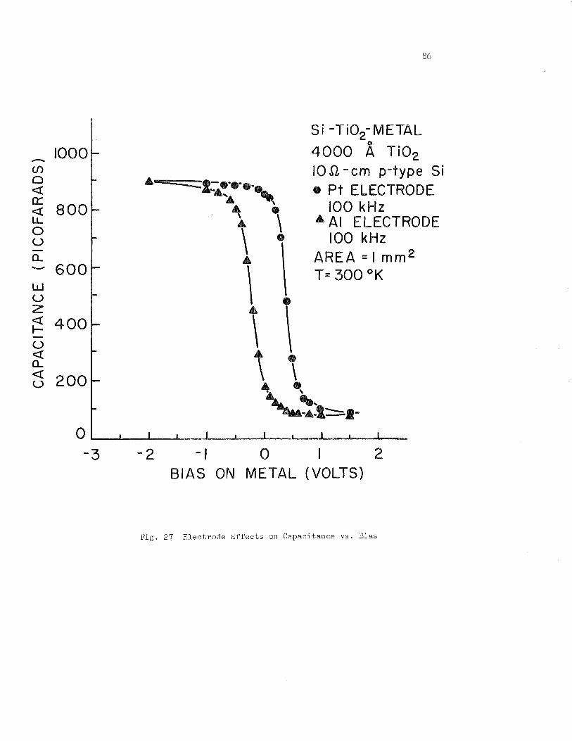
IOQ-c rn p-type Si @ P t ELECTRODE
100 kHz i \ r A l ELECTRODE
\ 100 kHz
i i AREA = l mm2 T= 300 O K
0 - 3 - 2 - I 0 I 2
B I A S ON M E T A L (VOLTS)
Fig. 27 Electrode E f f e c t s on Capacitance vs . Bias
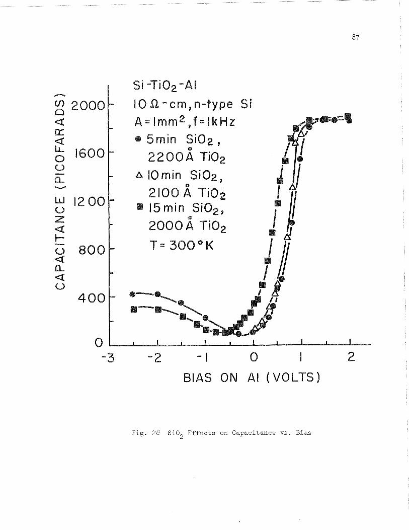
Fig . 28 S i O E f f e c t s on Capacitance v s . Bias 2
negat ive s t a t e s . Analogous e f f e c t s a r e seen f o r s i l i c o n d ioxide-s i l icon
43 n i t r i d e mixtures . No h y s t e r e s i s e f f e c t i s observed i n making t h e C-V measurements a s
w i th Si3N4. Hys te re s i s would be observed when t h e r e i s an apprec iab le
dens i ty of s t a t e s deep i n t h e oxide having t ime cons tan ts longer than t h e
time it t akes t o vary t h e b i a s because t h e charging and d ischarg ing of
t h e s e s t a t e s would l a g behind t h e b i a s var ia t ion lo ' , The f a c t t h a t no hys-
t e r e s i s i s observed means t h a t t h e dens i ty of s t a t e s i n t h e oxide having
time cons tan ts of t h e o r d e r of minutes i s n e g l i g i b l e .
The preceding cons ide ra t ions i n d i c a t e t h a t nega t ive su r f ace charges
e x i s t wi th in t h e Ti0 f i lm . The dens i ty of slow oxide su r f ace s t a t e s i s 2
approximately 10" sta tes /cm2. The dens i ty of f a s t i n t e r f a c e su r f ace
s t a t e s i s about 10'' s t a t e s / e ~ - c m 2 near t h e band edge and about 1011 s t a t e s /
Z eV-cm near t h e c e n t e r of t h e band. D i f f e ren t frequency c h a r a c t e r i s t i c s
a r e observed depending on the organometal l ic used t o form t h e f i lms . S h i f t s
i n t h e capaci tance-vol tage c h a r a c t e r i s t i c s near V = 0 wi th d i f f e r e n t metal
e l e c t r o d e s and with mixtures of Ti02 - SiO i n d i c a t e unique device poss i - 2
b i l i t i e s .

CHAPTER V I I
SUMMARY AWD CONCLUSIONS
The r e s u l t s of t h i s work form a cons i s t en t p i c t u r e of t h e growth
and behavior of t h e t i t a n i u m dioxide f i lms formed by chemical va,por depo-
s i t i o n . Hydrolysis of t i t a n i u m organometal l ics i n a hydrogen and carbon
dioxide atmosphere a t high temperature forms phys i ca l ly and e l e c t r i c a l l y
s a t i s f a c t o r y t i t a n i u m dioxide f i l m s .
This research inc ludes t h e design and cons t ruc t ion of a vapor depo-
s i t i o n system t o grow Ti0 The growth technique i s new, however, it i s 2
50 s i m i l a r t o a technique used by Feuersanger . The thermodynamic considera-
t i o n s a i d i n t h e ana lys i s of t h e process and l e a d t o t h e de te rmina t ion of
t h e optimum ope ra t ing cond i t i ons . The r e a c t i o n u t i l i z e d var ious organo-
m e t a l l i c s of t i t a n i u m , and t e t r a i s o p r o p y l t i t a n a t e proves t o be t h e most
s u i t a b l e due t o i t s high vapor p r e s s u r e .
Subs t r a t e s a r e plat inum coated qua r t z and po l i shed s i l i c o n , bo th
n-type and p-type. Fas t neutron a c t i v a t i o n ana lys i s f i n d s t h a t t h e s t o i -
chiometry of t h e f i lms depends on the depos i t ion condi t ions . Films formed
a t temperatures l e s s than 850°C a r e oxygen d e f i c i e n t .
A s tudy of t h e phys i ca l p r o p e r t i e s of t h e f i lms i n d i c a t e s t h a t t h e
f i lms appear hard , smooth, and r e f l e c t i v e . An x-ra,y s tudy i n d i c a t e s t h a t
t h e f i lms a r e p o l y c r y s t a l l i n e Ti0 The f i l m adherence t o t h e s u b s t r a t e 2
i s e n t i r e l y s a t i s f a c t o r y . Forty-eight pe r cent hydro f luo r i c a c i d e tches
t h e f i lms a t about 700 angstroms p e r minute and tends t o cause some pee l -
i ng . The e l e c t r i c a l c h a r a c t e r i s t i c s do not change during room temperature
s to rage and moisture t e s t s . The r e f r a c t i v e index , as determined by e l l i p -
sometry, i s about 2 . 0 .
A major r e s u l t of t h i s work i s a knowledge of t h e conduction be-
havior of t i t a n i u m dioxide f i lms on s i l i c o n and metal s u b s t r a t e s . The
89
depos i t ion temperature s t rong ly in f luences t h e conduct iv i ty of t h e s e f i lms .
The oxygen d e f i c i e n t f i lms a r e more semiconducti ng than i n s u l a t i n g . Ex-
per imenta l ly , t h e cu r r en t i s p ropor t iona l t o exp (mE 'I2) where m i s a con-
s t a n t and E i s t h e e l e c t r i c f i e l d . The cur ren t -vol tage c h a r a c t e r i s t i c s
f o r M I M s t r u c t u r e s a r e independent of p o l a r i t y f o r metals wi th d i f f e r e n t
work func t ions i n d i c a t i n g bulk c o n t r o l l e d emission. These cons idera t ions
i n d i c a t e t h a t ' t h e dominant conduction mechanism i n t i t a n i u m dioxide i s Poole-
Frenkel emission from donor and acceptor s i t e s and t r a p s w i th in t h e bulk of
t h e Ti02 f i lm . The s i t e s l i e approximately 0.25 eV from t h e band edge.
Both donor and accep to r s i t e s a r e p re sen t c r e a t i n g a compensating e f f e c t .
The breakdown s t r e n g t h of t h e s e f i lms i s 5 x l o 5 vol ts /cm.
Another major r e s u l t of t h i s work i s a knowledge of t h e s i l i c o n -
t i t an ium dioxide system as determined from capaci tance-vol tage charac te r -
i s t i c s of an MOS c a p a c i t o r s t r u c t u r e . Energy s t a t e s e x i s t at t h e i n t e r f a c e
between t h e s i l i c o n and t h e t i t an ium dioxide . These s t a t e s become sources
of charge s t rong ly a f f e c t i n g t h e dev ice ' s p r o p e r t i e s . The C-V d a t a i n d i c a t e
t h a t negat ive su r f ace charges e x i s t w i th in t h e Ti0 f i l m . The dens i ty of 2
slow oxide su r f ace s t a t e s i s approximately 1012 s ta tes /cm2. The dens i ty
of f a s t i n t e r f a c e su r f ace s t a t e s i s about 1012 states/eV-cm2 near t h e band
edge and about 10" states/eV-cm2 near t h e cen te r of t h e band a s determined
by t h e f la t -band v a r i a t i o n with temperature method of Gray and Brown60, t h e
100,101 equiva len t p a r a l l e l conductance method of Nicol l ian and Goetzberger
12 5 and t h e capaci tance d i spe r s ion method of Terman . The d i e l e c t r i c cons tan t of t h e s e f i lms i s 80 on plat inum and 50
on s i l i c o n due t o t h e presence of a t h i n l a y e r of SiO on t h e s i l i c o n . 2
D i f f e ren t frequency c h a r a c t e r i s t i c s a r e observed i n t h e C-V curves de-
pending on t h e organometa l l ic used t o form t h e f i lms .
S h i f t s i n t he capaci tance-vol tage c h a r a c t e r i s t i c s near V = 0 wi th
d i f f e r e n t meta l e l ec t rodes and wi th mixtures of Ti0 - SiO i n d i c a t e unique 2 2
device p o s s i b i l i t i e s . Herein l i e s a very promising a r e a f o r f u r t h e r s tudy .
Tne high d i e l e c t r i c cons tan t causes t h e abrupt change i n t h e C-V curve t o
occur very near zero v o l t s even f o r r a t h e r l a r g e d e n s i t i e s of su r f ace
s t a t e s . Figure 27 i l l u s t r a t e s t h e e f f e c t o f - a d i f f e r e n t work func t ion on
t h e C-V curves. By changing from aluminum t o plat inum e l ec t rodes one can
go from a dep le t ion mode device t o an enhancement mode device because wi th
plat inum e l e c t r o d e s a channel w i l l form on p-type m a t e r i a l wi th p o s i t i v e
b i a s . With aluminum t h e channel i s a l ready formed a t zero b i a s . This means
t h a t Ti0 could be used t o make an n-channel enhancement mode MOSFET which 2
i s nea r ly impossible t o do with SiO Building such a device would l e a d 2
t o such device parameters a s channel conduct iv i ty and turn-on vo l t age .
Figure 28 shows t h e e f f e c t of growing a l a y e r of SiO under t h e 2
Ti02. P o s s i b i l i t i e s e x i s t f o r f u r t h e r work here by s tudying mixtures of *
SiO - Ti0 - Si31\J4. C e r t a i n l y , t h e d i f f e r e n t types of s t a t e s and mechan- 2 2
isms a s soc i a t ed with t h e s e t h r e e i n s u l a t o r s . could c r e a t e i n t e r e s t i n g s h i f t s
and e f f e c t s on t h e MOS c h a r a c t e r i s t i c s and perhaps l e a d t o very u s e f u l de-
v i c e a p p l i c a t i o n s .
APPENDIX I
ATTEMPTS TO GROW LEAD TITANATE
Having e s t a b l i s h e d t h e optimum condi t ions f o r t h e depos i t ion of Ti0 2
at tempts were made t o grow PbTiO which might y i e l d improved d i e l e c t r i c prop- 3
e r t i e s . The a l k y l d e r i v a t i v e s of l e a d have s u f f i c i e n t v o l a t i l i t y and s t a b i l -
i t y t o be very promising f o r such an a p p l i c a t i o n . T e t r a e t h y l l e a d , ( C H ) Pb, 2 5 4
and Tet ra i sopropyl t i t a n a t e , ( C H 0 ) Ti , should form PbTiO The l e a d and ti- 3 7 4 3 '
taniwn compounds a r e l i q u i d s a t room temperature and have s u f f i c i e n t vapor
p re s su re t o permit t h e r a t e of de l ive ry of t h e r e spec t ive gas t o t h e r e a c t o r
t o be c o n t r o l l e d by r e g u l a t i o n of t h e flow of c a r r i e r gas over t he l i q u i d .
The vapor pressure and p r o p e r t i e s of t e t r a e t h y l l e a d a r e c l o s e l y s i m i l a r t o
t e t r a i s o p r o p y l t i t a n a t e . The source of t h e t e t r a e t h y l l e a d i s t h e E thy l Cor-
p o r a t i on,
The p l an o f a t t a c k was t o grow l e a d oxide from t h e t e t r a e t h y l l e a d
and e s t a b l i s h a growth r a t e s i m i l a r t o t h a t of t h e a l ready s t u d i e d Ti0 and 2
then combine t h e two t o form PbTiO Problems occurred i n t h e growth of t h e 3"
PbO due t o t h e low mel t ing p o i n t s of var ious forms o f l e a d oxide. When ope-
r a t i n g a t temperatures around 900°C, requi red f o r t h e H + CO r e a c t i o n t*o go 2 2
t o completion, no l e a d oxide i s formed because t h e mel t ing i s between 300'-
800°C f o r var ious forms of l e a d oxide , A t temperatures around 500°C a cloudy
f i l m of poor appearance i s formed, bu t it i s su-spected t h a t t h i s f i l m could
be oxygen d e f i c i e n t a s were Ti0 f i lms formed a t low temperatures . 2
With equal flow r a t e s of t e t r a i s o p r o p y l t i t a n a t e (TPT) and t e t r a -
e t h y l l e a d (TEL) a t g0o0C nothing forms, Turning o f f t h e TEL allows a f i l m
of Ti0 t o form, bu t t u r n i n g on t h e TEL aga in s tops t h e growth, The PbO i s 2
apparent ly keeping t h e Ti0 and PbTiO from forming a t high temperatures . 2 3

The conclusion of t h i s a t tempt i s t h a t l e a d t i t a n a t e cannot, be grown
e a s i l y i n a iI 2
+ C02 a.tmosphere because of t h e low me l t ing p o i n t of t h e PbO
and t h e high temperature r equ i r ed f o r t h e H + CO r e a c t i o n . Lower tempera- 2 2
t u r e depos i t i on i n an oxygen atmosphere o r i n a moist atmosphere from a water
bubbler might be a p l a u s i b l e approach t o t h i s problem.
BIBLIOGRAPHY
History and Review
1. J . N . B l i cke r and J . H . Oxley, "CVD Opens New Horizons i n Ceramic Technol- ogy," BUU. ~ m . Ceram. ~ o c . 4 1 ( 2 ) , 81 (1962) .
2 , R. Glang and S. Wajda, "Vapor Growth i n Semiconductor Technology," Met. ~ o c . Conf. 1 5 , 27 (1961) .
3. A . J . Mountvala and S.L. Blum, "Chemical Vapor Deposition f o r Elec t ron Devices," ~ e s e a r c h / ~ e v e l o p m e n t , 34 ( J U ~ Y 1966) .
4. H.E. Poda l l and M , M , Mi t che l l , Jr- , "The Use of Organometallic Com- pounds i n Chemical Vapor Deposi t ion," Ann. N . Y . Acad, Sc i . 125 ( l) , 218 (1965).
5. C.F. Powell , I .E . Campbell, B.W. Gonser, Vapor P l a t i n g , John Wiley and Sons, B a t t e l l e Memorial I n s t i t u t e , Electrochemical S e r i e s (1955)~
6. C,F, Powell , J . H . Oxley, J . M . Blocher , Vapor Deposi t ion, John Wiley and Sons, B a t t e l l e Memorial I n s t i t u t e , Electrochemical S e r i e s (1966).
7. E.M, Sherwood ( B a t t e l l e ) , "Vapor P l a t i n g , " P l a t i n g 52, 667 (1965).
8. E.M. Sherwood and J . M . Blocher , Jr . ( B a t t e l l e ) , " ~ a p o - ~ e t a l l u r g y : I Vapor Deposi t ion [of ~ e t a l s ] : The F i r s t Hundred Years , I T J . Metals 17 ( 6 ) , 594 (1965) . -
D i e l e c t r i c Review
9. P.A, Larssen, on-linear D i e l e c t r i c s ," I n s u l a t i o n 338 (May/June 66 ) .
10 . A.R. von Hippel , e t a l . , "High D i e l e c t r i c Constant Mater ia l s and Ferro- e l e c t r i c i t y 1 ' - Fina l Report No. AFCRL 6392 Contract AF 1906-6155, AD 404776 ( ~ a r . , 1963).
11. A. R. von Hippel , "High-Dielectric Constant Mater ia l s as Capaci tor D i - e l e c t r i c s ," Technical Report 1 4 5 , MIT Lab I n s u l . Res . ( ~ e c , 1959) .
12 . A.R. von Hippel Ed. , D i e l e c t r i c Mater ia l s and Appl ica t ions , Technical P r e s s , MIT, Wiley, (1954).
Thermodynamics
13. American Chemical Soc ie ty , Metal-Organic Compounds, a c o l l e c t i o n of papers composing t h e Symposium on Metal-Organic Compounds of t h e Am. Chem. Soc. A p r i l , 1957. Adv, Chem, S e r , 23.

D O C , Bradley, R . G a ~ e and We Wardlaw, "S t ruc tu re Aspects of t h e Hydrol- y s l s of Tizanium Alkoxides ," J. Chem. Soc. , 469 ( l 9 5 7 ) .
R c W o Coutmt , N , A l b m , J , F , M i l l e r , "Study of t h e Mechanisms o f Pyrol- y t i c Deposi t ion," ( ~ a t t e l l e ) AD 468055 ( ~ u g u s t 1965) .
H , C , B r i l l , "Organo-t i tanates ," TAPPI 38, No, 5 , 1 4 1 A (1955).
B u l l e t i n of t he Titanium Pigment Corp . ( N a t i m e Lead Co . Dow Chemical Company, JANAF Thermochemicsal Tables (1960 t o d a t e ) ,
Handbook of Chemistry and Phys ics , 39th e d i t i o n , Chemical Rubber Pub- l i s h i n g Co,, 1958,
H , C , Kaufman, Handbook of OrganometaLlic Compounds, Van Nostrand, I n c , , New York , (1961)~
Parks , Free Energies of Some Organic Compounds, N.Y.: Chemical Cata- l o g Coo (1932)"
K.S. P i t z e r and L. Brewer, Thermodynamics ( ~ e w i s and anda all), New York : McGraw-Hill 11961 ) ,
E, G. Rochow, Organome*~all i- Chemistry, Reinhold Publ. Co. , N , Y . ( 1964)~
F,D, Rossini , e t a l . , Se lec t ed Values of Phys ica l and Thermodynamic P rope r t i e s of Hydrocarbons and Related Compo-mds , Pi t t sbu rgh : Carnegie P r e s s , (1953) .
H , Scha f fe r , Chemical Transport React ions, Academic P r e s s , N , Y . (1964) .
CVD and Die lec t . r i c Mater ia l s
Roger Argenal-Ara,u.z , " ~ o m ~ o s i t i o n of Thin TimOn F i ~ n l s by Fast Ne11 t r a n Act iva t ion Analysis , ' I Master Thesls , Univers i ty of Texas at* Aus t in ( June , 1968) .
T , Arizumi and T, Nishinaga, "Transport Reaction i n a Closed Tube Pro- ce s s , " Japan JAP 4 ( 3 ) , 165 (1965) .
C , R , Barnes and C , R . Gasner, "F'yrolytic Deposition of S102 f o r 6 0 0 ' ~ Thin Film Capazi tors ," J . Electrochemical Soc. 110, 361 (May 1963).
IC.E, Bean, P.S, Gleim and W.R. Rimyan, "Some P r o p e r t i e s of Vapor Depos- i t e d S i N Films Using SiH4-NH3-H2 System," presented a t Electrochemi- 3 4 ca? Socle ty Meeting i n Ph i l ade lph ia , October 9-14, 1966,
I<,E, Bean and P ,S , Gleim, "some P rope r t i e s of Vapor Deposited S i c , " J. Electrochem. Soco 1 1 4 , 1158 (1967) .
31" J , Black, D. Peterson , W . Brand, "Vapor Phase Deposition Methods f o r Metal Oxide Based D i e l e e t r i r s , " AD 450131 ( O c t . , 1964) .
J , Black, D. Pe te rson , W . Brand, "Vapor Phase Deposition Techniques f o r Fab r i ca t ion of Microe lec t ronic C i r c u i t r y Thin Film Elements," AD 456793 an. 1965) .
D,M. Brown and P , V. Gray, "MOS Science and Technology , I t General E l e c t r i c Research and Development Center , Rept. #67-C-026 (1967) .
G , A . Brown, W , C , Robine t te , Jr. and H . G . Carlson, " ~ l e c t r i c a l Character- i s t i c s of S i N Films ," J . Electrochem. Soc. 115 , 948 (1968).
3 4 R.M. Burger and R,P. Donovan, Fundamentals of S i l i c o n I n t e g r a t e d Device Technology, P r e n t i c e H a l l , Englewood, N . J . , (1967) .
E.G, Bylander, "Kinet ics of S i l i c o n C r y s t a l Growth from SiC14 Decomposi- t i o n , " J , Electrochem, Soc . , 109 , 1171 (1962)~
D.R. Cal laby, "sur face Layer of BaTiO JAP, 37, 2295 (May 1966) . 3 '
R.W, Chr i s ty , " E l e c t r i c a l P r o p e r t i e s of Thin Polymer Fi lms, P a r t 11, Thickness 50-150A ," J . Appl. Phys , , 35, 2179 (1964) .
T, L. Chu and G.A. Grubec , " S i l i c a Films by Chem-Transport , I t Trans. AIME 223, 568 (1965).
T,L, Chu, C , H , Lee, J , R . Szedon, "Films of S i l i c o n Ni t r ide-Si l icon Diox- i d e Mixtures ," presented a t t h e Dallas Meeting of t h e Electrochemical Soc ie ty , May 1 0 , 1967, Abs t rac t No, 83.
B e J. Cur t i s and J . A , Wilkinson, "Prepara t ion of Mixed Oxide Crys t a l s by Chemical Transport React ions," J. Am. Cel-am, Soc, 4 8 , 49 (1965).
P. D. Davidse and L. I . Maisse l , " D i e l e c t r i c Thin Films through r f Sput- t e r i n g , " JAP 37, 574 (1966) .
B,E, Deal , P . J , Fleming and P.L. Cas t ro , " ~ l e e t r i c a l P rope r t i e s of Vapor Deposited S i N and SiO Films," J.Electrochem. Soc. 1 1 5 , 300 (1968).
3 4 2
A . J , Dekker, S o l i d S t a t e Phys ics , Prent ice-Hal l , Englewood C l i f f s , New Jersey (1957).
R.P. Donovan, I n t e g r a t e d S i l i c o n Device Technology, Vol. X I I I , I n t r a - connections and I s o l a t i o n , RTI, AD 655 081 ( ~ a y 1967) .
P.R. Emtage, "~nhancement of Metal t o I n s u l a t o r Tunneling by Op t i ca l Phonons," J , Appl. Phys. , 38, 1820 (1967) .
P.R, Emtage and W , Tantraporn, " ~ c h o t t k ~ Emission Through Thin I n s u l a t - i ng ~ i l m s , " Phys. Rev. L e t t , , 8 , 267 (1962) .
G , Ferment and N , J . Haske l l , "Fabr ica t ion of Beryllium Oxide Radomes by P y r o l y t i c Deposi t ion ," AD 608486 (June 30, 1964) .
49. A, E, Feuersanger and D , R , F rankl , "Hrigh Frequency Surface V a r a ~ t ~ o r s , I t
IEEE Trans, on Elec t ron Devices, ED-10, 143 (1963) .

A, E* Feuersanger , "Titanium Dioxlde D i e l e c t r i c Films Prepared by Vapor Reaction," Proc, IEEE 52 (121, 1463 (1964).
E. To F l t zgibbons , Current Mechanisms i n Thin Polymer Fi lms, Master ' s Thesis , The Univers i ty of Texas a t Aus t in , Aus t in , Texas, June, 1967.
R , I , Frank and J , G . Simmons, "Space-Charge E f f e c t s on Emission-Limited Current Flow i n I n s u ~ a t o r s , " J e Appl. Phys , , Vol. 38, No. 2 , Feb. 1967, pp, 832-840,
D. R , Frank1 , "Some Ef fec t s of Ma te r i a l Parameters on Surface Varactors ," S o l i d S t a t e E lec t ron ic s 2 , 71 (1961) .
J e Frenkel , "Pre-~reakdown Phenomena, I n s u l a t o ~ s and Semiconduetors , I 1
Phys* Rev., 54, 657 (1938) -
ReE. Gannon, R C n F o l i v e i l e r , T. Vas i lo s , " ~ ~ r o l y t ~ i c Synt,hesis of Ti- tanium Diboride ," J. Am- Ceram, Sot? 46 ( l o ) , 496 (1963) ,
G. C O B o G a r r e t t and W . H , B r a t t a i n , "Phys ica l Theory of Semi conductors Surfaces , I 1 Phys - Rev, , Vol. 99, No. 2 , pp, 376-388, J u l y 1 5 , 1955.
J, J. Gebhardt and R.F. Cree, "Vapor Deposited Borides of Group I V A Metals , I 1 J, Am, Ceram. Soc. 48, 262 (1965 1 and AD 601861.
R , M o G l a i s t e r , "So l id Solu t ion D i e l e c t r i c s Based on Sodium Niobate , I 1
J- Amc Ceram, Soc. 43, 348 ( i 9 6 0 ) .
F,R. Gleason, Jr- and L*R. Watson, " F e r r i t e Films Prepared by Pyrohydrol- y t i c Deposition ," JAP 34, 1217 (1963).
P.V, Gray and D,M. Brown, "Density of SiO -Si I n t e r f a c e Stat.es , I ' Appl. ~ h y s . ~ e t t e r s 8 , 3 1 (1966). 2
A , S, Grove, Physics and Technology of Semiconductor Devices, Wiley , Ch. 9 (1967) .
A. E* Grove, E. H . Snow, B, E. Deal and C , T. Sah , "Simple Phys i ca l Model of t h e Space Charge Capacitance of Metal-Oxide-Semiconductor S t r u c t u r e s ," J, Appl. Phys. , Val. 35, No. 8 , pp. 2458, Aug., 1964.
G , Haas , "Prepa ra t ion , P rope r t i e s and Op t i ca l Applicat ion of Thin Films of Ti0 " TTaeuum, 2 , 331 (1952) .
2
L,E, Hal lander , Jr , and P e Lt, Cas t ro , " D i e l e c t r i c P rope r t i e s of S ing le Crys t a l Nonstoichiornetric R u t i l e , Ti02," JAP 33, 3421 11962).
L, Holland, Vacuum Deposi t ion of Thin Fil-ms , Wiley : New York, N a y . 473 (1.960 ) .
66. J , J, Hanak, K . S t r a t e r , G . W o Cullen, "Prepara t ion and P r o p e r t i e s of Va- por Deposited Niobium Stannide ( ~ b ~ n ) , " RCA Rev, 25 ( 3 ) , 342 (1964) .
3

D , R . Harbison and H.L. Taylor , "Chemical Vapor Deposition of Thin Film D i e l e c t r i c s ," Southwestern IEEE Conference Record, Hov.ston , Texas
D.R . Harbison and H . Lo Taylor , "chemical Vapor Deposition of Thin Film Titanium Dioxide, " J . ~yec t rdchem. Soc, 115, 238: ( ~ u ~ u s t , 1968) t o be
i n Deposited Thin Film D i e l e c t r i c Mater ia l s by t h e Electrochem- i c a l Soc ie ty ,
D.R. Harbison , J . R , Yeargan, and H . L . Taylor , "MOS CapaciLance-Dissipa- t i o n P r o p e r t i e s , " Southwestern IEEE Conference Record, D a l l a s , Texas (1966),
T,E, Hartman, J , C , B l a i r , and R e Bauer , " E l e c t r i c a l Conduction Through sio ~ i h s , " J , Appl, ~ h y s - , 37, 2468 (1966).
T.E. Hartman and J , S . Chivian, "Elec t ron Tunneling Through Thin Aluminum Oxide Films," Phys, Rev., 134, ~ 1 0 9 4 (1964).
W.H. Hartwig and R , R . Richard, "MIS ADC and D i g i t a l Transducer Concepts ," Government Microc i rcu i t Appl ica t ions Conference Digest of Papers , I , 378 (Oct , 1-3, 1968) .
S,M. H u , D , R , Kerr , and L , V e Gregor, "Evidence of Hole I n j e c t i o n and Trapping i n S i l i c o n N i t r i d e Films Prepared by Reactive Spu t t e r ing , " Appl, ~ h y s . L e t t , , 10, 97 (1967) .
F, Huber, "Thin Films of Ti Oxide f o r Microminia tur iza t ion ," IEEE Trans. Component P t s . CP-11, #2 , 38 (1964) .
I I T Research I n s t i t u t e , "Charac ter iza t ion of Ceramic Mate r i a l s f o r Micro- e lec t ronic : Appl ica t ions ," P r o j e c t G 6006-6, Rept. #2 (June 1966) .
V.J. Jennings , A Sommers, H , C . Chang, " E p i t a x i a l Growth of s ic ," J . Elec- trochem, Soc, 113, 728 (1966) .
I. T, Johansen, " E l e c t r i c a l Conduct ivi ty i n Evaporated S i l i con Oxide Fi lms, J , Appl- Phys . , 37, 499 (1966) .
B,A. Joyce, e t al. , "The Epi tax i .a l Deposit.ion of S i on Quartz and ~ l u m i n a , " Trans AIME 233, 556 (1965) .
1 .L- Kalnin and J, Rosenstock, "Vapor Deposition of Ge on Mo," J. Elec- chem. Soc. 112, 329 (1965) .
J , K l e r e r , "On t h e Mechanism of t h e Deposition of S i l i c a by Pyro ly t i c Depos i t i on of S i l a n e s ," J . Electrochem. Soc , 112, 503 (1965) .
T. K , Lakshmanan , "Chemical Formation of Mic roc i r cu i t Elements ," AD 428590 ( ~ e c , 1963) .
D , R , Lamb, E l e c t r i c a l Conduction Mechanisms i n Thin I n s u l a t i n g F i l ~ , London, Methuen, 1967.
I t , L e h ~ ~ r e c , 4 - Slobodskoy and J . L . Sprague, ' 'F ie ld E f fec t Capacitance Analysis 9f S ~ ~ r f a c e S t a t e s on S i l i c o n , " Phys, S t a t , Soc, , 7101, 3 , pp, 447-464, 1963.
R , Lindner, emic icon duct or Surface Varactor , I 1 B.S. T . J , , Vole 4 1 , No, 3 , May, 1962,
M n Macha, "A Review of Ceramic Thin Film Technology , I 1 Tech, Repor t , No, A F M L - T R - ~ ~ - ~ ~ ~ (1967) .
H, T, Mann , " ~ l e c t r i c a l P r o p e r t i e s of Thin Polymer Fi lms, P a r t I . Tbick- ness 5 0 0 - ~ ~ o o A , " J , Apple Fhys" , 35, 2173 (1964) .
A, Many, Y Golds te in , N , B. Grover, Semi conductor Su r faces , North- Holland Publ i sh ing Co, Amsterdam 1965,
Paul M Marcus, " C a l c i l l a t i ~ n af" t h e C a p a ~ i t ~ a n c e of a Semiconductor - Surface , wl th Applr:ation t o S ~ l i c o n , " I , B , M , J a u r n a l , Vol. 8 , No, 5 , pp. 496-505, NO^. , 1964,
H ,B , Mar t in , " ~ e v e ~ o ~ m o n of Mi- roe lee t ronlc C i r c u i t s f o r Linear Ap- p l i c a + i o n s ," AD 287650 (Oct , 1962) .
J. Maserjian and C o A , Mead, "Conduction through Ti0 Thin Films with Large I o n i c Space Charge ," J. Phys. Chem. Sol ids 282 1971 119671.
IC,H, Ma.m~ell and L,H, Robm.in, "Chemical Vapor Deposi t ion of Oxide -
Films from V o l a t i l e Chlorides T Si02 ," E1ectr.o-hem. Technol, 3 , 37 (1965)
F. L- McCrackln, Em Passag l in , R . R . Stromberg and H.L. S t e inbe rg , "Mea- s u r e m e n h f t h e Thickness and Ref rac t ive Index of Very Thin Films and t h e Op t i ca l P rope r t i e s of Surfaces by El l ipsometry ," J, of R e s e a ~ c h , A, Phys and Chem-, VolhC 6 7 A , No, 4 , July-Aug., 1963, pp. 363-377.
C o A n Mead, "Electron Transport Mechanisms i n Thin I n s u l a t i n g Fi lms, Phys , Rev, , 128, 2088 ( 1.962) . D m Meyorhofer an3 S , Ochs, " ~ u r r e n t Flow i n Very Thin Films o f Al. O and B ~ O , I 1 J , Appl, Phy S , , 34, 2535 (1963 1. 2 3
J , J n Mibehel l , "prepara t ion and Dielectric Prope r t i e s of a Multl-@om- ponent Me ta l l i c Oxide ~ i l m , " An 416330 arch. 1963) .
N,F, Mott and R , W , Gurney, E l e c t r o n i c Processes i n I o n i c C r y s t a l s , Dover Pub l i ca t ions , Inc , New York (1964) .
E , K , Mu-iler, B , J - Nicholson, G . LIE Turner , "The E x p i a q of BaTiO Films by Vapor Deposi t ion," B r i t , JAF 1 3 , 486 (1962). 3
E,K. Muller , B, J , Nicholson, G . L'E Turner, "The E p i t a x i a l Vapor Deposition of Perovski te Materials," J. Electrochem. Soc. 110 , 969 (1963) -
EaHo Nico l l i an and A. Goetzberger, "La te ra l AC Current Flow Model f o r MOS Capaci tors ," IEEE Trans. E.D. , ED-12, 108 (1965).
E, H, Nico l l i an and A , Goet zberger , "MOS Conductance Technique f o r Measur- i ng Surface S t a t e Parameters , I t ~ p p . ~ h y s . L4et t . 7, 216 (1965) e
E.H. N ico l l i an and A , Goetzberger, he Si-SiO I n t e f a c e - E l e c t r i c a l 2
P rope r t i e s as Determined by t h e Conductance Technique," BSTJ 46, 1055 (1967).
J.J, OtDwyer, "Current-Voltage C h a r a c t e r i s t i c s of D i e l e c t r i c Fi lms," J . ~ p p l . ~ h y s . , 37 , 599 (1966) .
D. Pe t e r son , J. Black, W . Brand, D . Dulaney, "Non Vacuum Deposition Technique f o r Use i n Fab r i ca t ing Thin Film C i r c u i t s , " AD 462743 ( A p r i l 1965) .
D . R , Pe t e r son , Black, Brand, To l l i ve r ( ~ o t o r o l a S/C ~ i v . ) "Techniques f o r Vapor P l a t i n g Passive Film Components on S i l i c o n I n t e g r a t e d C i r c u i t Wafers , I 1 AD 475622, (Nov. 1965) .
S. R . Pol lack and C .E, Morris , " ~ l e c t r o n Tunneling Through Asymmetric Films of Thermally Grown Al2O3 , I f J . Appl. Phys . , 35, 1503 (1964).
S.R, Po l l ack , "Schottky F i e l d Emission Through I n s u l a t i n g Layers," J. Appl, ~ h y s , , 34, 877 (1963) .
M , Rand and J .L , Ashworth, "Deposition of S i l i c a Films on Ge by t h e CO Process , I 1 J . Electrochem, Soc. 113, 48 (1966) .
2
H , G , Rylander 111, "El l ipsometr ic measurement,^ , I t I n t e r n a l Report , E l ec t ron ic Ma te r i a l s Research Lab, The Univers i ty of Texas, Aus t in , Texas,
C-T. Sah, R. Noyce, and W . Shockley, "Car r i e r Generation and Recombin- a t i o n i n P-N Juncti .ons," Proc IRE 45, 1228 (1957 ) .
P a s e Scha f fe r , ch valuation of Vapor Deposition Growth of Oxide S ing le Crys t a l s from Metal Halides ," AD 616914 ( ~ a y , 1965 ) . F, W e Schrnidlin, "Enhanced Tunneling Through D i e l e c t r i c Films due t o I o n i c Defects ," J . Appl. Phys 37, 2823 (1966) ,
A , C , Schaf fhauser , ed. Proceedings of t h e Conference on Chemical Vapor Deposition of Refrac tory Metals , Alloys, and Compounds, h e l d a t Gat l inburg , Tenn., September 12-14, 1967.
MsS. S e l t z e r , N o Albon, B. P a r i s , R . C . Himes, "Microscopic Measurement of S t ep Movement During C r y s t a l Growth by Chemical Vapor Deposi t ion," Rev. S c i . I n s t r . 36, 1423 (1965) .
W , H , Shepherd, "Vapor Phase Deposition and Etching of S i l i c o n , I 1 J . Elec- trochem, Soc. 112 , 988 (1965) .
V. J.. S i l v e s t r l , "Gr~wth Rate and Doping i n t h e GeC14-H2 System," pre- sent,ed a t t he Dal las Meeting of t h e Electrochemical Socie ty Meetlng, Ab- s t r a c t No, 1 0 4 , May 1 2 , 1967,
J , G , Slmmons, "Generalized Formula f o r t h e E l e c t r i c Tunnel E f f e c t Be- tween S lml l a r Elec t rodes Separated by a Thin I n s u l a t i n g Fllm," J . Appl. Phys , Vo1. 311, No, 6 , June , 1963, pp. 1793-1803.
J - G o Simmons, " P o o l e - ~ r e n k e l E f f e c t and Schoirtky E f f e c t i n Metal-Insilia- tor-Metal Systems," Phys, Rev , , 155 , 657 (1967) .
J . G . Simmons, " P o t e n t i a l B a r r i e r s and Emission-Limited Current Flow Be- tween CLosely Spaced P a r a l l e l Metal Eleet,rodes ," J. Appl. Phys . , Volt 35, No, 8, Au.g, 1964, pp- 2472-2481.
R , A - Smlth, Semicond:lctovs, Cambridge Univ, P r e s s , Cambridge, (1959?
S. S t e e l e , J Poppls , R o E l l i s , La, Ragen, H . S e h i l l e r , "Progress Report on Chemi -a l Vapor Ileposi+,ed Materials f o r Elec t ron Tubes , I 1 AD 477126,
H , F, S t e r l i n g m d R e C . G. Swa,nn , "Chemical Vapor Deposi t lon Promoted by RF Discharge," S o l i d S ta+e Elec t ron 8 , 653 (1965).
H,F, S t e r l i n g and R , C O G . Swann, "RF I n i t i a t e d Vapor Deposi t ion of GI-assy Layer," Phys, Chem? Gl-asses 6 , 109 11965)-
R , S t r a t t o n , "Val"-Current C h a r a c t e r i s t i r s f o r Tunneling Through Insu-lat- i n g Fllms," J. Phys" Ckiem, S o l l d s , Vol. 23, 1963, pp. 1177-1190.
S ,M, Sze , " C u r r e n ~ Transport and Maximum D i e l e c t r i c S t rength of S i l i c o n N i t r i d e Films," Jo Appl* Phys. 38, 2951 (1967) .
Lo M, Terman, "An Inves t igc i t i 2n of Surf ace S t a t e s at. a S i l i c o n l S i l i c o n Oxide I n t e r f a c e Employing M-O-S Df odes ," Dissertation , Univers i ty Micrs- f i l m s , 1nc. , Ann Arbor, Mlchigm,
H , C , Theurer, "Ep i t ax i a l SI F i h s by Hydrogen Reducti on of S i c 1 " J . 4' - Electrochem. Soe, 108, 649 (1961) .
H, C * Theurer and H . Chr l s tensen , "Ep i t ax i a l Films of SI and Ge by h'allde Reduetian ," J , Electronhem, So?, 107, 268c (1960) .
J, J, T i e t j e n and J . A , Amlck, "The P r e p a r a t i on and P r o p e r t i e s of Vapor Deposited Epitaxial . GaAs by Using Arsine and Phosphine," J- Electrochem, Soc, 113, 72L 11966 ) ,
S,K, Tung and R-E, Caff rey , "The Deposition of Oxide on S t by React ion of a Metal Ha.Lide wi th a Hydrogea/Carbon Dioxide Nixt>ure," Trans. Met, Soc, AIME 233, 512 (1965) a
, B u l l e t i n of E. I . duPont de Nemours and Company, Wilmington, Delaware.
131. J , A. van Raal te , "Conduction Ph.enomena i n R u t i l e S ing le Crys t a l s , I 1 AD 610101, (1964) ,
132, A , R , von Hippel , "Studies on t h e Formation and P r o p e r t i e s of High Tempera- t u r e D i e l e c t r i c s ," AD 459511 (1964).
133* LoC. Wang, " ~ l e c t r i c a l Conduction Mechanisms i n Metal-Polymer-Semiconduc- t o r Thin Film S t r u c t u r e s , " Master ' s Thes i s , The Univers i ty of Texas a t Aust in, Aust in, Texas (1968) .
134. C , W. Wilmsen , " ~ u n n e l i n ~ from a Metal i n t o a semi conductor , I 1 D isser ta - t i o n , The Univers i ty of Texas, January, 1967,
135. J.J. Wortmm, I n t e g r a t e d S i l i c o n Device Technology, Vol. 111 -- Photo- engraving, AD 603715 (1964) .
136. J . R e Yeargan and H,L. Taylor , "Conduction Mechanisms of P y r o l y t i c S i l i - con N i t r i d e Fi lms," J . Electrochem. Soc, 115, 273 (1968) .
137. J. R , Yeargan and H . L o Taylor , h he Poole-Frenkel E f fec t with Compensa- t i o n Present , " J. Appl. Phys. (NOT. 1968).
138. M I Yokozawa, "Vapor Deposition of Ti0 , I t Japan JAF 7 , 96 (1968) . 2
139. A, Zawadowski, "General Theory of Tunneling i n Oxide Diodes," Phys. Rev, 163 , 341 (1967). -
140, C. Z i eg le r , itaxi axial In-Sb Films by Vapor Phase Transport Reaction ," S o l i d S t a t e E lec t ron ic s 6 , 680-81 (1963) .


![Nanoporous TiO2 and WO 3 Films by Anodization of ...1].pdfNanoporous TiO2 and WO 3 Films by Anodization of Titanium and Tungsten Substrates: Influence of Process Variables on Morphology](https://img.pdfslide.net/doc/110x75/60c30184963cb974b75d82dd/nanoporous-tio2-and-wo-3-films-by-anodization-of-1pdf-nanoporous-tio2-and.jpg)