Embed Size (px)
Citation preview
SANDIA REPORT SAND2012-2938 Unlimited Release Printed April 2012
First principles predictions of intrinsic defects in aluminum arsenide, AlAs: Numerical Supplement
Peter A. Schultz
Prepared by Sandia National Laboratories Albuquerque, New Mexico 87185 and Livermore, California 94550 Sandia National Laboratories is a multi-program laboratory managed and operated by Sandia Corporation, a wholly owned subsidiary of Lockheed Martin Corporation, for the U.S. Department of Energy's National Nuclear Security Administration under contract DE-AC04-94AL85000.
Approved for public release; further dissemination unlimited.
2
Issued by Sandia National Laboratories, operated for the United States Department of Energy by Sandia Corporation. NOTICE: This report was prepared as an account of work sponsored by an agency of the United States Government. Neither the United States Government, nor any agency thereof, nor any of their employees, nor any of their contractors, subcontractors, or their employees, make any warranty, express or implied, or assume any legal liability or responsibility for the accuracy, completeness, or usefulness of any information, apparatus, product, or process disclosed, or represent that its use would not infringe privately owned rights. Reference herein to any specific commercial product, process, or service by trade name, trademark, manufacturer, or otherwise, does not necessarily constitute or imply its endorsement, recommendation, or favoring by the United States Government, any agency thereof, or any of their contractors or subcontractors. The views and opinions expressed herein do not necessarily state or reflect those of the United States Government, any agency thereof, or any of their contractors. Printed in the United States of America. This report has been reproduced directly from the best available copy. Available to DOE and DOE contractors from U.S. Department of Energy Office of Scientific and Technical Information P.O. Box 62 Oak Ridge, TN 37831 Telephone: (865) 576-8401 Facsimile: (865) 576-5728 E-Mail: [email protected] Online ordering: http://www.osti.gov/bridge Available to the public from U.S. Department of Commerce National Technical Information Service 5285 Port Royal Rd. Springfield, VA 22161 Telephone: (800) 553-6847 Facsimile: (703) 605-6900 E-Mail: [email protected] Online order: http://www.ntis.gov/help/ordermethods.asp?loc=7-4-0#online
3
SAND2012-2938 Unlimited Release Printed April 2012
First principles predictions of intrinsic defects in aluminum arsenide, AlAs:
Numerical Supplement
Peter A. Schultz Advanced Device Technologies, Dept. 1425
Sandia National Laboratories P.O. Box 5800
Albuquerque, New Mexico 87185-MS1322
Abstract
This Report presents numerical tables summarizing properties of intrinsic defects in aluminum arsenide, AlAs, as computed by density functional theory. This Report serves as a numerical supplement to the results published in: P.A. Schultz, “First principles predictions of intrinsic defects in Aluminum Arsenide, AlAs”, Materials Research Society Symposia Proceedings 1370 (2011; SAND2011-2436C), and intended for use as reference tables for a defect physics package in device models.

4
This page intentionally left blank
5
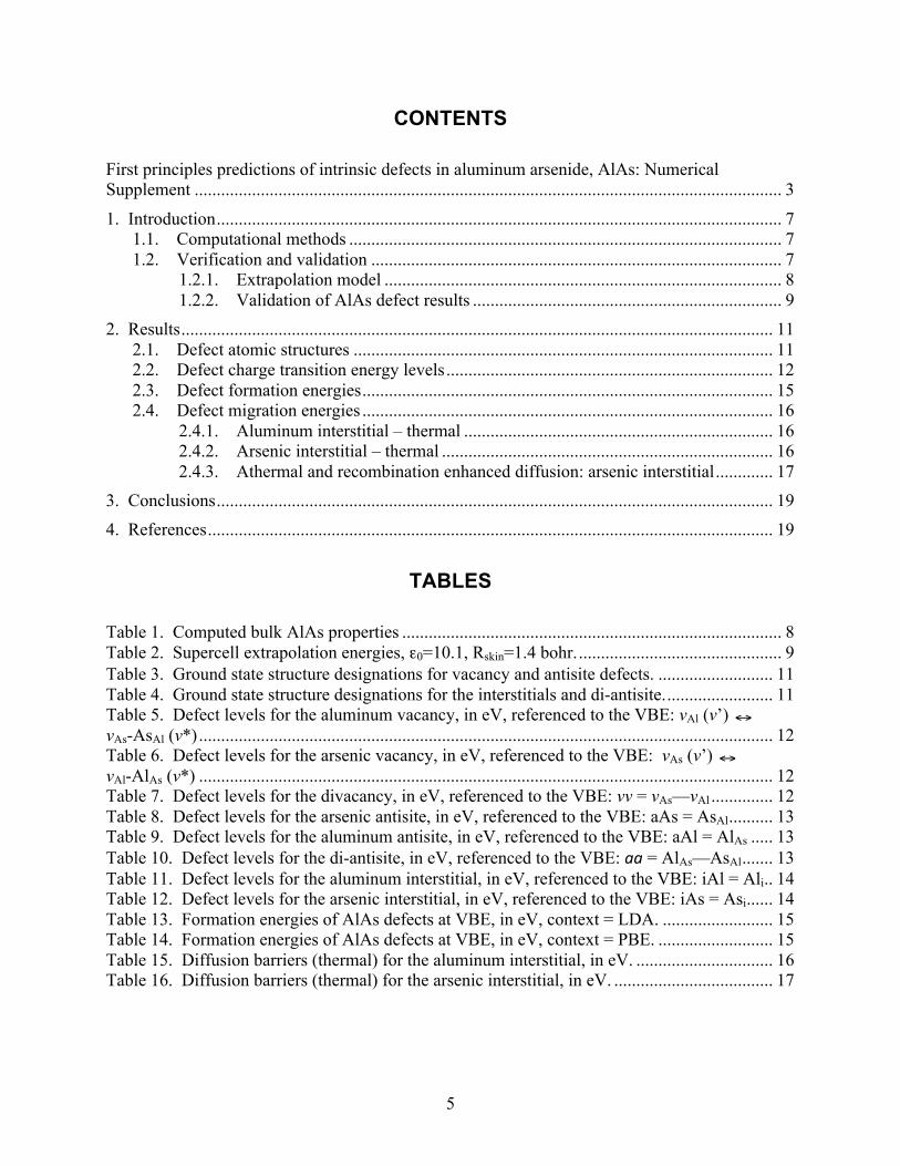
CONTENTS
First principles predictions of intrinsic defects in aluminum arsenide, AlAs: Numerical Supplement ..................................................................................................................................... 31. Introduction................................................................................................................................ 7
1.1. Computational methods .................................................................................................. 71.2. Verification and validation ............................................................................................. 7
1.2.1. Extrapolation model .......................................................................................... 81.2.2. Validation of AlAs defect results ...................................................................... 9
2. Results...................................................................................................................................... 112.1. Defect atomic structures ............................................................................................... 112.2. Defect charge transition energy levels.......................................................................... 122.3. Defect formation energies............................................................................................. 152.4. Defect migration energies ............................................................................................. 16
2.4.1. Aluminum interstitial – thermal ...................................................................... 162.4.2. Arsenic interstitial – thermal ........................................................................... 162.4.3. Athermal and recombination enhanced diffusion: arsenic interstitial............. 17
3. Conclusions.............................................................................................................................. 194. References................................................................................................................................ 19
TABLES Table 1. Computed bulk AlAs properties ...................................................................................... 8Table 2. Supercell extrapolation energies, ε0=10.1, Rskin=1.4 bohr............................................... 9Table 3. Ground state structure designations for vacancy and antisite defects. .......................... 11Table 4. Ground state structure designations for the interstitials and di-antisite......................... 11Table 5. Defect levels for the aluminum vacancy, in eV, referenced to the VBE: vAl (v’)
€
↔ vAs-AsAl (v*).................................................................................................................................. 12Table 6. Defect levels for the arsenic vacancy, in eV, referenced to the VBE: vAs (v’)
€
↔ vAl-AlAs (v*) .................................................................................................................................. 12Table 7. Defect levels for the divacancy, in eV, referenced to the VBE: vv = vAs—vAl .............. 12Table 8. Defect levels for the arsenic antisite, in eV, referenced to the VBE: aAs = AsAl.......... 13Table 9. Defect levels for the aluminum antisite, in eV, referenced to the VBE: aAl = AlAs ..... 13Table 10. Defect levels for the di-antisite, in eV, referenced to the VBE: aa = AlAs—AsAl....... 13Table 11. Defect levels for the aluminum interstitial, in eV, referenced to the VBE: iAl = Ali.. 14Table 12. Defect levels for the arsenic interstitial, in eV, referenced to the VBE: iAs = Asi...... 14Table 13. Formation energies of AlAs defects at VBE, in eV, context = LDA. ......................... 15Table 14. Formation energies of AlAs defects at VBE, in eV, context = PBE. .......................... 15Table 15. Diffusion barriers (thermal) for the aluminum interstitial, in eV. ............................... 16Table 16. Diffusion barriers (thermal) for the arsenic interstitial, in eV. .................................... 17
6
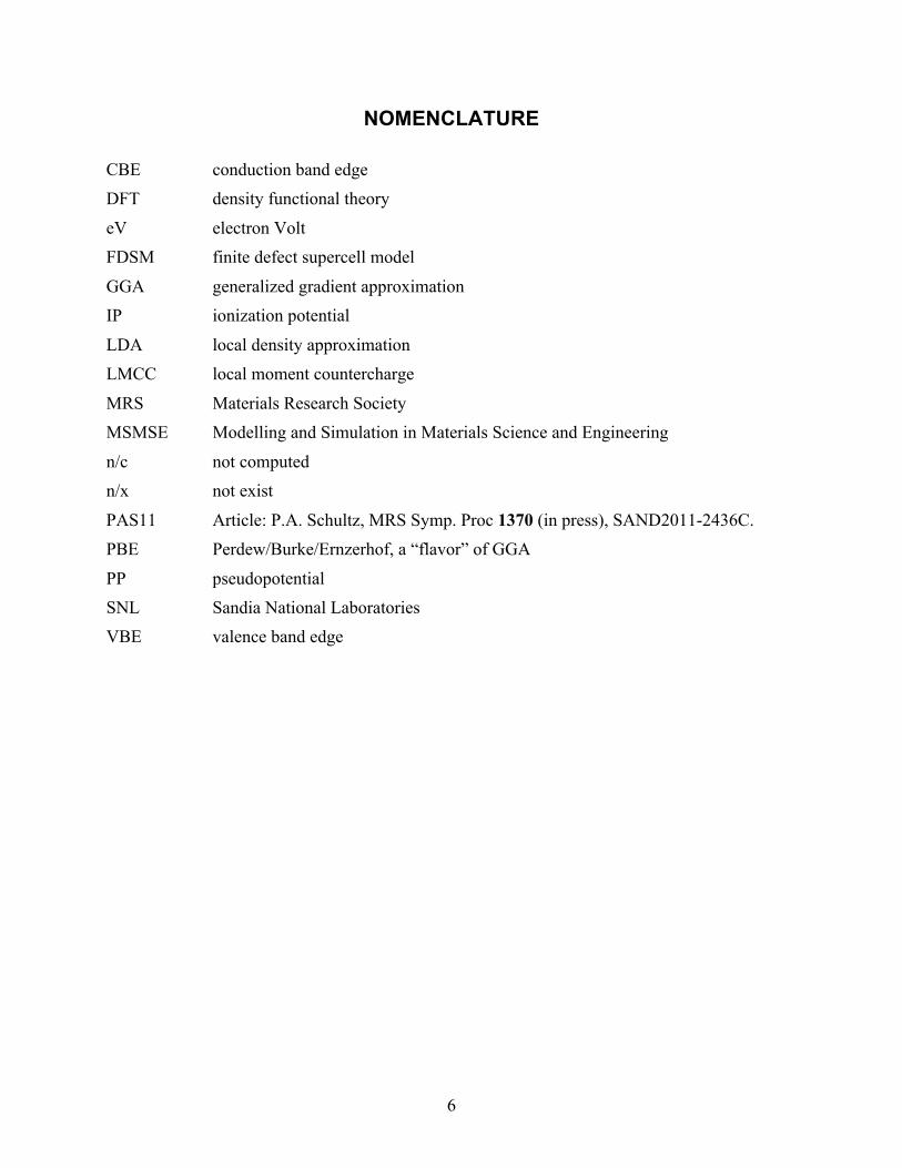
NOMENCLATURE
CBE conduction band edge DFT density functional theory
eV electron Volt FDSM finite defect supercell model
GGA generalized gradient approximation IP ionization potential
LDA local density approximation LMCC local moment countercharge
MRS Materials Research Society MSMSE Modelling and Simulation in Materials Science and Engineering
n/c not computed n/x not exist
PAS11 Article: P.A. Schultz, MRS Symp. Proc 1370 (in press), SAND2011-2436C. PBE Perdew/Burke/Ernzerhof, a “flavor” of GGA
PP pseudopotential SNL Sandia National Laboratories VBE valence band edge
7
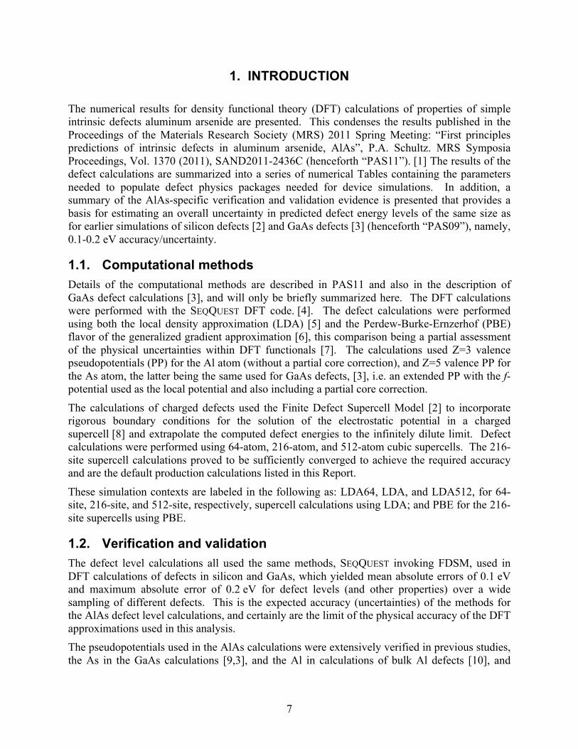
1. INTRODUCTION
The numerical results for density functional theory (DFT) calculations of properties of simple intrinsic defects aluminum arsenide are presented. This condenses the results published in the Proceedings of the Materials Research Society (MRS) 2011 Spring Meeting: “First principles predictions of intrinsic defects in aluminum arsenide, AlAs”, P.A. Schultz. MRS Symposia Proceedings, Vol. 1370 (2011), SAND2011-2436C (henceforth “PAS11”). [1] The results of the defect calculations are summarized into a series of numerical Tables containing the parameters needed to populate defect physics packages needed for device simulations. In addition, a summary of the AlAs-specific verification and validation evidence is presented that provides a basis for estimating an overall uncertainty in predicted defect energy levels of the same size as for earlier simulations of silicon defects [2] and GaAs defects [3] (henceforth “PAS09”), namely, 0.1-0.2 eV accuracy/uncertainty.
1.1. Computational methods Details of the computational methods are described in PAS11 and also in the description of GaAs defect calculations [3], and will only be briefly summarized here. The DFT calculations were performed with the SEQQUEST DFT code. [4]. The defect calculations were performed using both the local density approximation (LDA) [5] and the Perdew-Burke-Ernzerhof (PBE) flavor of the generalized gradient approximation [6], this comparison being a partial assessment of the physical uncertainties within DFT functionals [7]. The calculations used Z=3 valence pseudopotentials (PP) for the Al atom (without a partial core correction), and Z=5 valence PP for the As atom, the latter being the same used for GaAs defects, [3], i.e. an extended PP with the f-potential used as the local potential and also including a partial core correction.
The calculations of charged defects used the Finite Defect Supercell Model [2] to incorporate rigorous boundary conditions for the solution of the electrostatic potential in a charged supercell [8] and extrapolate the computed defect energies to the infinitely dilute limit. Defect calculations were performed using 64-atom, 216-atom, and 512-atom cubic supercells. The 216-site supercell calculations proved to be sufficiently converged to achieve the required accuracy and are the default production calculations listed in this Report.
These simulation contexts are labeled in the following as: LDA64, LDA, and LDA512, for 64-site, 216-site, and 512-site, respectively, supercell calculations using LDA; and PBE for the 216-site supercells using PBE.
1.2. Verification and validation The defect level calculations all used the same methods, SEQQUEST invoking FDSM, used in DFT calculations of defects in silicon and GaAs, which yielded mean absolute errors of 0.1 eV and maximum absolute error of 0.2 eV for defect levels (and other properties) over a wide sampling of different defects. This is the expected accuracy (uncertainties) of the methods for the AlAs defect level calculations, and certainly are the limit of the physical accuracy of the DFT approximations used in this analysis. The pseudopotentials used in the AlAs calculations were extensively verified in previous studies, the As in the GaAs calculations [9,3], and the Al in calculations of bulk Al defects [10], and
8
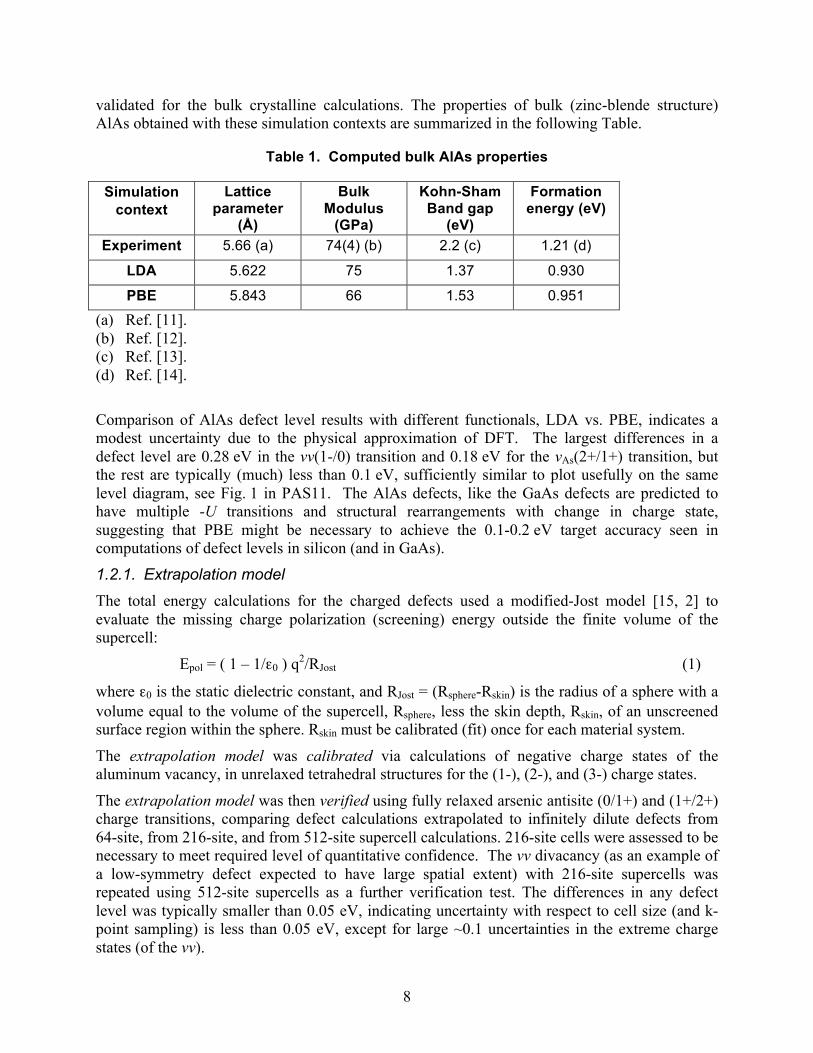
validated for the bulk crystalline calculations. The properties of bulk (zinc-blende structure) AlAs obtained with these simulation contexts are summarized in the following Table.
Table 1. Computed bulk AlAs properties
Simulation context
Lattice parameter
(Å)
Bulk Modulus
(GPa)
Kohn-Sham Band gap
(eV)
Formation energy (eV)
Experiment 5.66 (a) 74(4) (b) 2.2 (c) 1.21 (d)
LDA 5.622 75 1.37 0.930
PBE 5.843 66 1.53 0.951
(a) Ref. [11]. (b) Ref. [12]. (c) Ref. [13]. (d) Ref. [14].
Comparison of AlAs defect level results with different functionals, LDA vs. PBE, indicates a modest uncertainty due to the physical approximation of DFT. The largest differences in a defect level are 0.28 eV in the vv(1-/0) transition and 0.18 eV for the vAs(2+/1+) transition, but the rest are typically (much) less than 0.1 eV, sufficiently similar to plot usefully on the same level diagram, see Fig. 1 in PAS11. The AlAs defects, like the GaAs defects are predicted to have multiple -U transitions and structural rearrangements with change in charge state, suggesting that PBE might be necessary to achieve the 0.1-0.2 eV target accuracy seen in computations of defect levels in silicon (and in GaAs).
1.2.1. Extrapolation model The total energy calculations for the charged defects used a modified-Jost model [15, 2] to evaluate the missing charge polarization (screening) energy outside the finite volume of the supercell:
Epol = ( 1 – 1/ε0 ) q2/RJost (1)
where ε0 is the static dielectric constant, and RJost = (Rsphere-Rskin) is the radius of a sphere with a volume equal to the volume of the supercell, Rsphere, less the skin depth, Rskin, of an unscreened surface region within the sphere. Rskin must be calibrated (fit) once for each material system.
The extrapolation model was calibrated via calculations of negative charge states of the aluminum vacancy, in unrelaxed tetrahedral structures for the (1-), (2-), and (3-) charge states.
The extrapolation model was then verified using fully relaxed arsenic antisite (0/1+) and (1+/2+) charge transitions, comparing defect calculations extrapolated to infinitely dilute defects from 64-site, from 216-site, and from 512-site supercell calculations. 216-site cells were assessed to be necessary to meet required level of quantitative confidence. The vv divacancy (as an example of a low-symmetry defect expected to have large spatial extent) with 216-site supercells was repeated using 512-site supercells as a further verification test. The differences in any defect level was typically smaller than 0.05 eV, indicating uncertainty with respect to cell size (and k-point sampling) is less than 0.05 eV, except for large ~0.1 uncertainties in the extreme charge states (of the vv).
9
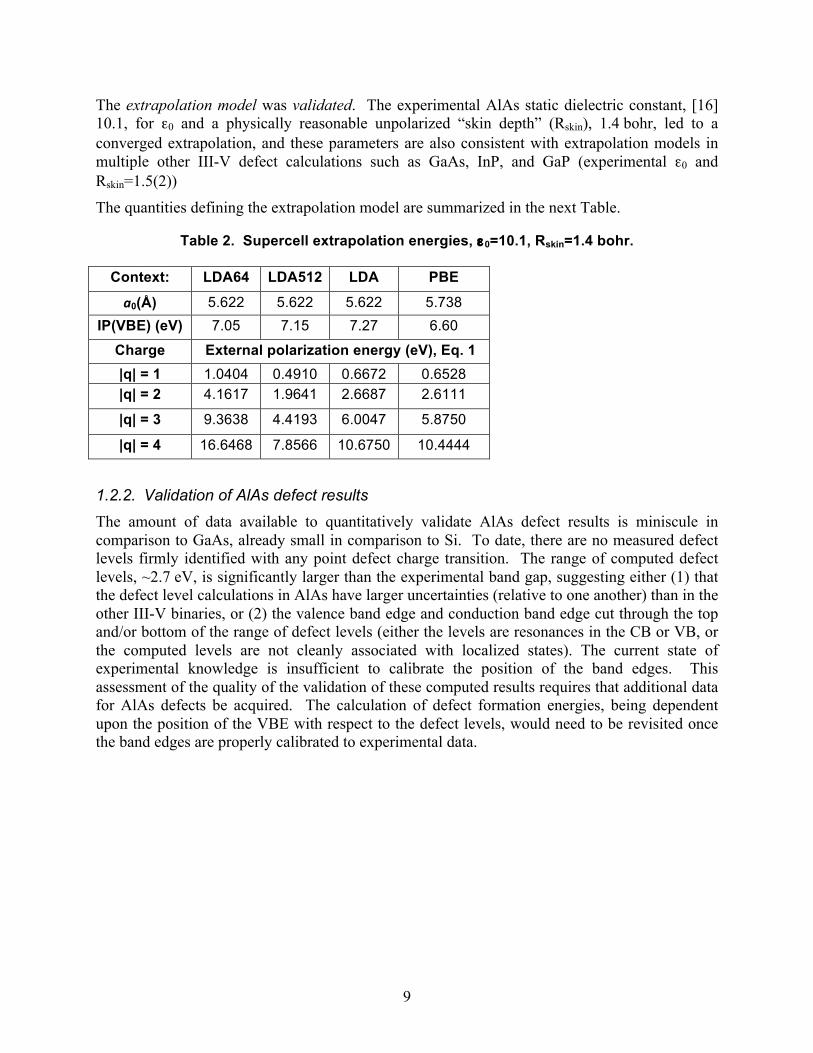
The extrapolation model was validated. The experimental AlAs static dielectric constant, [16] 10.1, for ε0 and a physically reasonable unpolarized “skin depth” (Rskin), 1.4 bohr, led to a converged extrapolation, and these parameters are also consistent with extrapolation models in multiple other III-V defect calculations such as GaAs, InP, and GaP (experimental ε0 and Rskin=1.5(2))
The quantities defining the extrapolation model are summarized in the next Table.
Table 2. Supercell extrapolation energies, ε0=10.1, Rskin=1.4 bohr.
Context: LDA64 LDA512 LDA PBE
a0(Å) 5.622 5.622 5.622 5.738 IP(VBE) (eV) 7.05 7.15 7.27 6.60
Charge External polarization energy (eV), Eq. 1 |q| = 1 1.0404 0.4910 0.6672 0.6528 |q| = 2 4.1617 1.9641 2.6687 2.6111
|q| = 3 9.3638 4.4193 6.0047 5.8750
|q| = 4 16.6468 7.8566 10.6750 10.4444
1.2.2. Validation of AlAs defect results The amount of data available to quantitatively validate AlAs defect results is miniscule in comparison to GaAs, already small in comparison to Si. To date, there are no measured defect levels firmly identified with any point defect charge transition. The range of computed defect levels, ~2.7 eV, is significantly larger than the experimental band gap, suggesting either (1) that the defect level calculations in AlAs have larger uncertainties (relative to one another) than in the other III-V binaries, or (2) the valence band edge and conduction band edge cut through the top and/or bottom of the range of defect levels (either the levels are resonances in the CB or VB, or the computed levels are not cleanly associated with localized states). The current state of experimental knowledge is insufficient to calibrate the position of the band edges. This assessment of the quality of the validation of these computed results requires that additional data for AlAs defects be acquired. The calculation of defect formation energies, being dependent upon the position of the VBE with respect to the defect levels, would need to be revisited once the band edges are properly calibrated to experimental data.

10
This page intentionally left blank
11
2. RESULTS
The section contains the Tables that summarize the numerical results for DFT simulations of defects in AlAs.
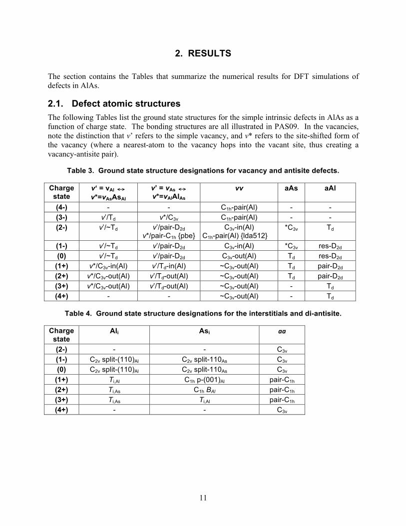
2.1. Defect atomic structures The following Tables list the ground state structures for the simple intrinsic defects in AlAs as a function of charge state. The bonding structures are all illustrated in PAS09. In the vacancies, note the distinction that v’ refers to the simple vacancy, and v* refers to the site-shifted form of the vacancy (where a nearest-atom to the vacancy hops into the vacant site, thus creating a vacancy-antisite pair).
Table 3. Ground state structure designations for vacancy and antisite defects.
Charge state
v‘ = vAl
€
↔ v*=vAsAsAl
v’ = vAs
€
↔ v*=vAlAlAs
vv aAs aAl
(4-) - - C1h-pair(Al) - - (3-) v’/Td v*/C3v C1h-pair(Al) - - (2-) v’/~Td v’/pair-D2d
v*/pair-C1h {pbe} C3v-in(Al)
C1h-pair(Al) {lda512} *C3v Td
(1-) v’/~Td v’/pair-D2d C3v-in(Al) *C3v res-D2d (0) v’/~Td v’/pair-D2d C3v-out(Al) Td res-D2d
(1+) v*/C3v-in(Al) v’/Td-in(Al) ~C3v-out(Al) Td pair-D2d (2+) v*/C3v-out(Al) v’/Td-out(Al) ~C3v-out(Al) Td pair-D2d (3+) v*/C3v-out(Al) v’/Td-out(Al) ~C3v-out(Al) - Td (4+) - - ~C3v-out(Al) - Td
Table 4. Ground state structure designations for the interstitials and di-antisite.
Charge state
Ali Asi aa
(2-) - - C3v (1-) C2v split-(110)Al C2v split-110As C3v (0) C2v split-(110)Al C2v split-110As C3v
(1+) Ti,Al C1h p-(001)Al pair-C1h (2+) Ti,As C1h BAl pair-C1h (3+) Ti,As Ti,Al pair-C1h (4+) - - C3v
12
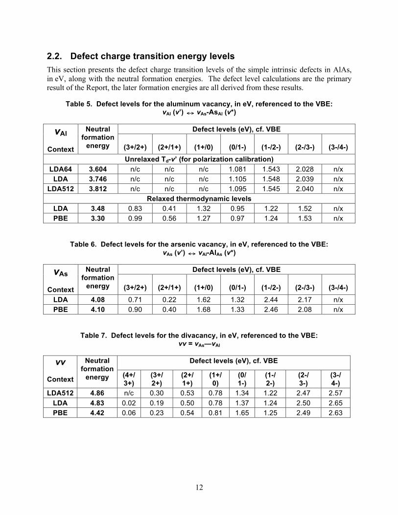
2.2. Defect charge transition energy levels This section presents the defect charge transition levels of the simple intrinsic defects in AlAs, in eV, along with the neutral formation energies. The defect level calculations are the primary result of the Report, the later formation energies are all derived from these results.
Table 5. Defect levels for the aluminum vacancy, in eV, referenced to the VBE: vAl (v’)
€
↔ vAs-AsAl (v*)
Defect levels (eV), cf. VBE vAl
Context
Neutral formation
energy
(3+/2+)
(2+/1+)
(1+/0)
(0/1-)
(1-/2-)
(2-/3-)
(3-/4-) Unrelaxed Td-v’ (for polarization calibration)
LDA64 3.604 n/c n/c n/c 1.081 1.543 2.028 n/x LDA 3.746 n/c n/c n/c 1.105 1.548 2.039 n/x
LDA512 3.812 n/c n/c n/c 1.095 1.545 2.040 n/x Relaxed thermodynamic levels
LDA 3.48 0.83 0.41 1.32 0.95 1.22 1.52 n/x PBE 3.30 0.99 0.56 1.27 0.97 1.24 1.53 n/x
Table 6. Defect levels for the arsenic vacancy, in eV, referenced to the VBE: vAs (v’)
€
↔ vAl-AlAs (v*)
Defect levels (eV), cf. VBE vAs
Context
Neutral formation
energy
(3+/2+)
(2+/1+)
(1+/0)
(0/1-)
(1-/2-)
(2-/3-)
(3-/4-) LDA 4.08 0.71 0.22 1.62 1.32 2.44 2.17 n/x PBE 4.10 0.90 0.40 1.68 1.33 2.46 2.08 n/x
Table 7. Defect levels for the divacancy, in eV, referenced to the VBE: vv = vAs—vAl
Defect levels (eV), cf. VBE vv
Context
Neutral formation
energy (4+/ 3+)
(3+/ 2+)
(2+/ 1+)
(1+/ 0)
(0/ 1-)
(1-/ 2-)
(2-/ 3-)
(3-/ 4-)
LDA512 4.86 n/c 0.30 0.53 0.78 1.34 1.22 2.47 2.57 LDA 4.83 0.02 0.19 0.50 0.78 1.37 1.24 2.50 2.65 PBE 4.42 0.06 0.23 0.54 0.81 1.65 1.25 2.49 2.63
13
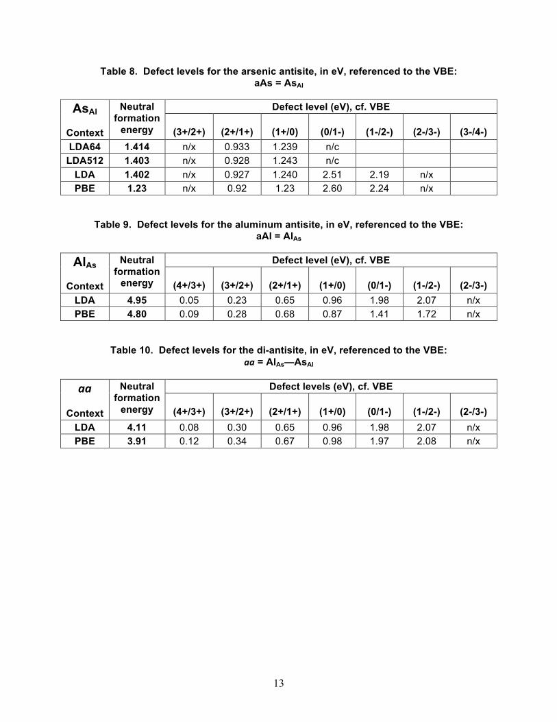
Table 8. Defect levels for the arsenic antisite, in eV, referenced to the VBE: aAs = AsAl
Defect level (eV), cf. VBE AsAl
Context
Neutral formation
energy
(3+/2+)
(2+/1+)
(1+/0)
(0/1-)
(1-/2-)
(2-/3-)
(3-/4-) LDA64 1.414 n/x 0.933 1.239 n/c
LDA512 1.403 n/x 0.928 1.243 n/c LDA 1.402 n/x 0.927 1.240 2.51 2.19 n/x PBE 1.23 n/x 0.92 1.23 2.60 2.24 n/x
Table 9. Defect levels for the aluminum antisite, in eV, referenced to the VBE: aAl = AlAs
Defect level (eV), cf. VBE AlAs
Context
Neutral formation
energy
(4+/3+)
(3+/2+)
(2+/1+)
(1+/0)
(0/1-)
(1-/2-)
(2-/3-) LDA 4.95 0.05 0.23 0.65 0.96 1.98 2.07 n/x PBE 4.80 0.09 0.28 0.68 0.87 1.41 1.72 n/x
Table 10. Defect levels for the di-antisite, in eV, referenced to the VBE: aa = AlAs—AsAl
Defect levels (eV), cf. VBE aa
Context
Neutral formation
energy
(4+/3+)
(3+/2+)
(2+/1+)
(1+/0)
(0/1-)
(1-/2-)
(2-/3-) LDA 4.11 0.08 0.30 0.65 0.96 1.98 2.07 n/x PBE 3.91 0.12 0.34 0.67 0.98 1.97 2.08 n/x
14
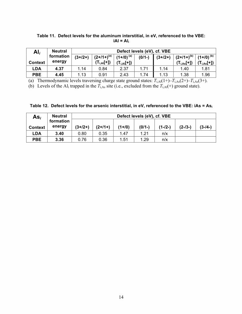
Table 11. Defect levels for the aluminum interstitial, in eV, referenced to the VBE: iAl = Ali
Defect levels (eV), cf. VBE Ali
Context
Neutral formation
energy (3+/2+) (2+/1+)(a)
(Ti,Al[+]) (1+/0) (a) (Ti,Al[+])
(0/1-) (3+/2+) (2+/1+)(b) (Ti,As[+])
(1+/0) (b) (Ti,As[+])
LDA 4.37 1.14 0.84 2.37 1.71 1.14 1.40 1.81 PBE 4.45 1.13 0.91 2.43 1.74 1.13 1.38 1.96
(a) Thermodynamic levels traversing charge state ground states: Ti,Al(1+)–Ti,As(2+)–Ti,As(3+). (b) Levels of the Ali trapped in the Ti,As site (i.e., excluded from the Ti,Al(+) ground state).
Table 12. Defect levels for the arsenic interstitial, in eV, referenced to the VBE: iAs = Asi
Defect levels (eV), cf. VBE Asi
Context
Neutral formation
energy
(3+/2+)
(2+/1+)
(1+/0)
(0/1-)
(1-/2-)
(2-/3-)
(3-/4-) LDA 3.40 0.80 0.35 1.47 1.21 n/x PBE 3.36 0.76 0.36 1.51 1.29 n/x
15
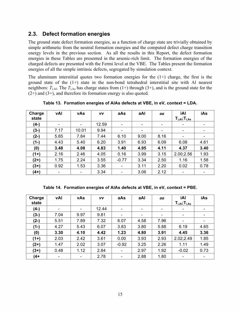
2.3. Defect formation energies The ground state defect formation energies, as a function of charge state are trivially obtained by simple arithmetic from the neutral formation energies and the computed defect charge transition energy levels in the previous section. As all the results in this Report, the defect formation energies in these Tables are presented in the arsenic-rich limit. The formation energies of the charged defects are presented with the Fermi level at the VBE. The Tables present the formation energies of all the simple intrinsic defects, segregated by simulation context. The aluminum interstitial quotes two formation energies for the (1+) charge, the first is the ground state of the (1+) state in the non-bond tetrahedral interstitial site with Al nearest neighbors: Ti,Al. The Ti,As has charge states from (1+) through (3+), and is the ground state for the (2+) and (3+), and therefore its formation energy is also quoted.
Table 13. Formation energies of AlAs defects at VBE, in eV, context = LDA.
Charge state
vAl vAs vv aAs aAl aa iAl Ti,Al;Ti,As
iAs
(4-) - - 12.59 - - - - - (3-) 7.17 10.01 9.94 - - - - - (2-) 5.65 7.84 7.44 6.10 9.00 8.16 - - (1-) 4.43 5.40 6.20 3.91 6.93 6.09 6.08 4.61 (0) 3.48 4.08 4.83 1.40 4.95 4.11 4.37 3.40
(1+) 2.16 2.46 4.05 0.16 3.99 3.15 2.00;2.56 1.93 (2+) 1.75 2.24 3.55 -0.77 3.34 2.50 1.16 1.58 (3+) 0.92 1.53 3.36 - 3.11 2.20 0.02 0.78 (4+) - - 3.34 - 3.06 2.12 - -
Table 14. Formation energies of AlAs defects at VBE, in eV, context = PBE.
Charge state
vAl vAs vv aAs aAl aa iAl Ti,Al;Ti,As
iAs
(4-) - - 12.44 - - - - - (3-) 7.04 9.97 9.81 - - - - - (2-) 5.51 7.89 7.32 6.07 4.58 7.96 - - (1-) 4.27 5.43 6.07 3.83 3.80 5.88 6.19 4.65 (0) 3.30 4.10 4.42 1.23 4.80 3.91 4.45 3.36
(1+) 2.03 2.42 3.61 0.00 3.93 2.93 2.02;2.49 1.85 (2+) 1.47 2.02 3.07 -0.92 3.25 2.26 1.11 1.49 (3+) 0.48 1.12 2.84 - 2.97 1.92 -0.02 0.73 (4+ - - 2.78 - 2.88 1.80 - -
16
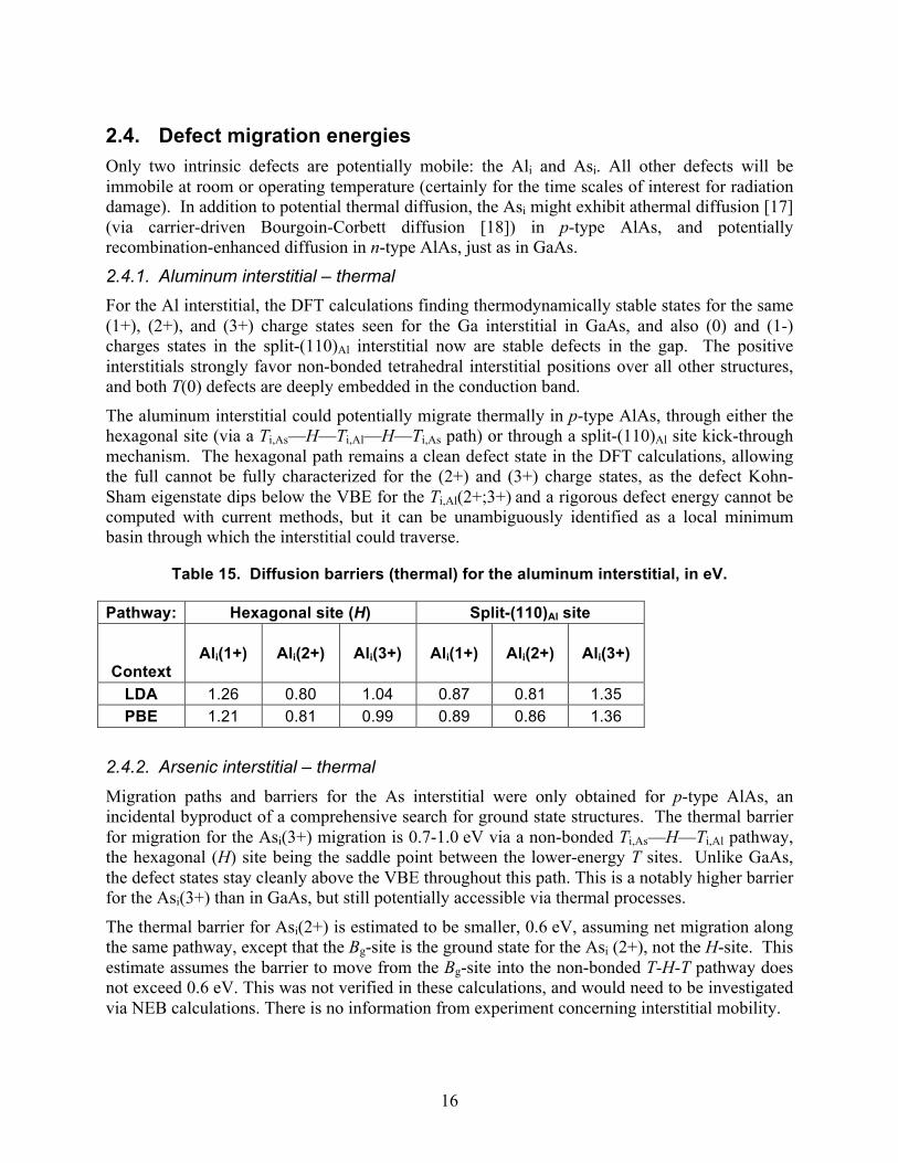
2.4. Defect migration energies Only two intrinsic defects are potentially mobile: the Ali and Asi. All other defects will be immobile at room or operating temperature (certainly for the time scales of interest for radiation damage). In addition to potential thermal diffusion, the Asi might exhibit athermal diffusion [17] (via carrier-driven Bourgoin-Corbett diffusion [18]) in p-type AlAs, and potentially recombination-enhanced diffusion in n-type AlAs, just as in GaAs.
2.4.1. Aluminum interstitial – thermal For the Al interstitial, the DFT calculations finding thermodynamically stable states for the same (1+), (2+), and (3+) charge states seen for the Ga interstitial in GaAs, and also (0) and (1-) charges states in the split-(110)Al interstitial now are stable defects in the gap. The positive interstitials strongly favor non-bonded tetrahedral interstitial positions over all other structures, and both T(0) defects are deeply embedded in the conduction band.
The aluminum interstitial could potentially migrate thermally in p-type AlAs, through either the hexagonal site (via a Ti,As—H—Ti,Al—H—Ti,As path) or through a split-(110)Al site kick-through mechanism. The hexagonal path remains a clean defect state in the DFT calculations, allowing the full cannot be fully characterized for the (2+) and (3+) charge states, as the defect Kohn-Sham eigenstate dips below the VBE for the Ti,Al(2+;3+) and a rigorous defect energy cannot be computed with current methods, but it can be unambiguously identified as a local minimum basin through which the interstitial could traverse.
Table 15. Diffusion barriers (thermal) for the aluminum interstitial, in eV.
Pathway: Hexagonal site (H) Split-(110)Al site
Context
Ali(1+)
Ali(2+)
Ali(3+)
Ali(1+)
Ali(2+)
Ali(3+)
LDA 1.26 0.80 1.04 0.87 0.81 1.35 PBE 1.21 0.81 0.99 0.89 0.86 1.36
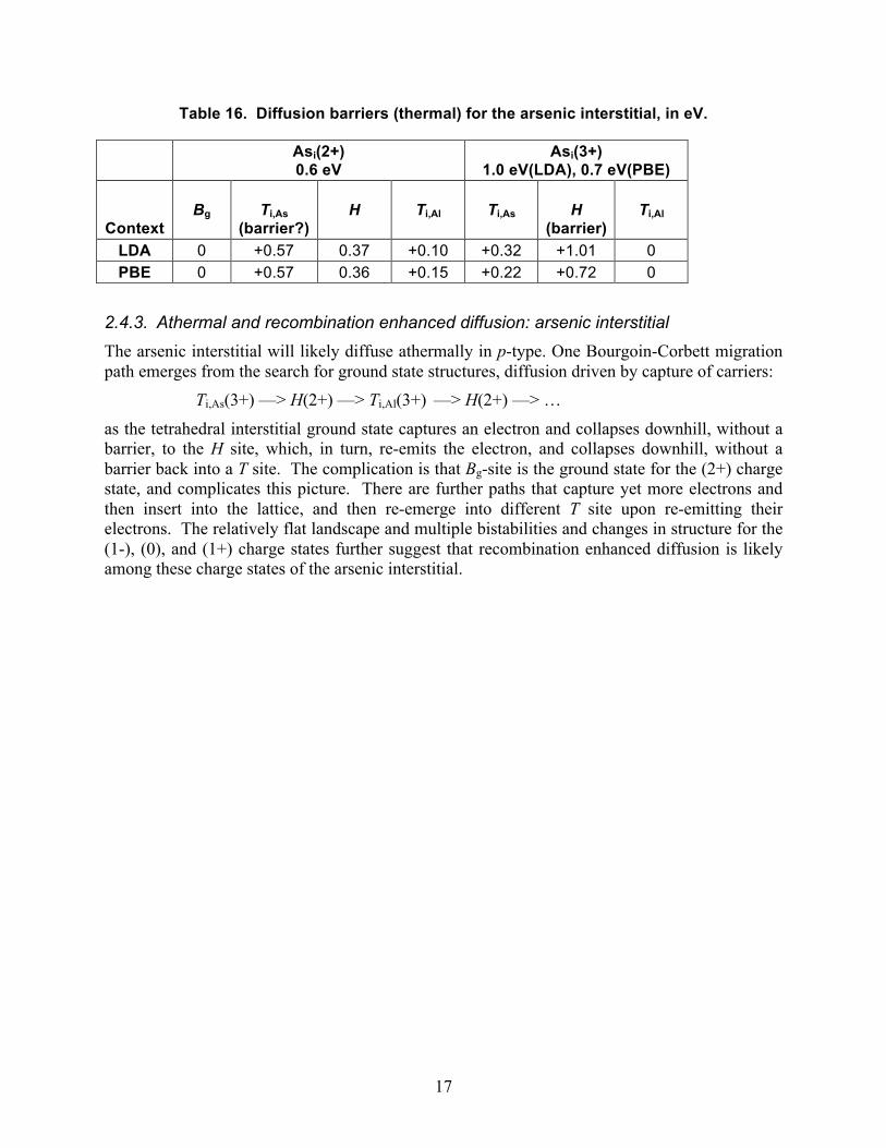
2.4.2. Arsenic interstitial – thermal
Migration paths and barriers for the As interstitial were only obtained for p-type AlAs, an incidental byproduct of a comprehensive search for ground state structures. The thermal barrier for migration for the Asi(3+) migration is 0.7-1.0 eV via a non-bonded Ti,As—H—Ti,Al pathway, the hexagonal (H) site being the saddle point between the lower-energy T sites. Unlike GaAs, the defect states stay cleanly above the VBE throughout this path. This is a notably higher barrier for the Asi(3+) than in GaAs, but still potentially accessible via thermal processes.
The thermal barrier for Asi(2+) is estimated to be smaller, 0.6 eV, assuming net migration along the same pathway, except that the Bg-site is the ground state for the Asi (2+), not the H-site. This estimate assumes the barrier to move from the Bg-site into the non-bonded T-H-T pathway does not exceed 0.6 eV. This was not verified in these calculations, and would need to be investigated via NEB calculations. There is no information from experiment concerning interstitial mobility.
17
Table 16. Diffusion barriers (thermal) for the arsenic interstitial, in eV.
Asi(2+) 0.6 eV
Asi(3+) 1.0 eV(LDA), 0.7 eV(PBE)
Context
Bg
Ti,As
(barrier?)
H
Ti,Al
Ti,As
H
(barrier)
Ti,Al
LDA 0 +0.57 0.37 +0.10 +0.32 +1.01 0 PBE 0 +0.57 0.36 +0.15 +0.22 +0.72 0
2.4.3. Athermal and recombination enhanced diffusion: arsenic interstitial The arsenic interstitial will likely diffuse athermally in p-type. One Bourgoin-Corbett migration path emerges from the search for ground state structures, diffusion driven by capture of carriers: Ti,As(3+) —> H(2+) —> Ti,Al(3+) —> H(2+) —> …
as the tetrahedral interstitial ground state captures an electron and collapses downhill, without a barrier, to the H site, which, in turn, re-emits the electron, and collapses downhill, without a barrier back into a T site. The complication is that Bg-site is the ground state for the (2+) charge state, and complicates this picture. There are further paths that capture yet more electrons and then insert into the lattice, and then re-emerge into different T site upon re-emitting their electrons. The relatively flat landscape and multiple bistabilities and changes in structure for the (1-), (0), and (1+) charge states further suggest that recombination enhanced diffusion is likely among these charge states of the arsenic interstitial.

18
This page intentionally left blank
19
3. CONCLUSIONS
The parameters needed to describe the defect properties of simple intrinsic defects in AlAs are summarized into Tables, tabulating the numerical results presented in PAS11.
4. REFERENCES
1. P.A. Schultz, MRS Symp. Proc. 1370, mrss11-1370-yy03-04 doi:10.1557/opl.2011.765 (2011).
2. P.A. Schultz, Phys. Rev. Lett. 96, 246401 (2006).
3. P.A. Schultz and O.A. von Lilienfeld, Modelling Simul. Mater. Sci. Eng. 17, 084007 (2009).
4. SEQQUEST code, unpublished, http://dft.sandia.gov/quest/ 5. J.P. Perdew and A. Zunger, Phys. Rev. 23, 5048 (1981).
6. J.P. Perdew, K. Burke, and M. Ernzerhof, Phys. Rev. Lett. 77, 3865 (1996). 7. A.E. Mattsson, P.A. Schultz, M.P. Desjarlais, T.R. Mattsson, and K. Leung, Modelling
Simul. Mater. Sci. Eng. 13, R1 (2005). 8. P.A. Schultz, Phys. Rev. B 60, 1551 (1999).
9. O.A. von Lilienfeld and P.A. Schultz, Phys. Rev. B 77, 115202 (2008). 10. A.E. Mattsson, R. Armiento, P.A. Schultz, and T.R. Mattsson, Phys. Rev. B 73, 195123
(2006). 11. R.P. Leavitt and F.T. Towner, Phys. Rev. B 48, 9154 (1993).
12. R.G. Green, H. Luo, T. Li, and A.L. Ruoff, Phys. Rev. Lett. 72, 2045 (1994). 13. C.A. Mead and W.G. Spitzer, Phys. Rev. Lett. 11, 358 (1963).
14. D.R. Lide (ed.), Handbook of Chemistry and Physics, 72nd Ed. (Boca Rotan: CRC Press, 1991).
15. W. Jost, J. Chem. Phys. 1, 466 (1933). 16. R.E. Fern and A. Onton, J. Appl. Phys. 42, 3499 (1971).
17. G.D. Watkins, in Radiation Damage in Semiconductors, ed. P. Baruch, p97 (Paris:Dunod, 1965).
18. J.C. Bourgoin and J.W. Corbett, Phys. Lett. A 38, 135 (1972).
20
DISTRIBUTION
(to be distributed electronically) 1 MS0899 Technical Library 9536 (electronic copy)
1 MS1179 L. J. Lorence 1341 ([email protected]) 1 MS1056 W. R. Wampler 1111 ([email protected])
1 MS1323 E. R. Keiter 1445 ([email protected]) 1 MS1315 J. S. Nelson 1131 ([email protected])
1 MS1189 T. R. Mattsson 1641 ([email protected]) 1 MS0457 R. A. Paulsen 2211 ([email protected])
1 MS1415 A. F. Wright 1131 ([email protected])