Embed Size (px)
Citation preview
Getting Started with the Virtex-7 FPGA VC707 Evaluation Kit
UG848 (v1.4.1) October 14, 2015
XPM 0402902-04
Getting Started with the VC707 Evaluation Kit www.xilinx.com UG848 (v1.4.1) October 14, 2015
The information disclosed to you hereunder (the “Materials”) is provided solely for the selection and use of Xilinx products. To the maximum extent permitted by applicable law: (1) Materials are made available "AS IS" and with all faults, Xilinx hereby DISCLAIMS ALL WARRANTIES AND CONDITIONS, EXPRESS, IMPLIED, OR STATUTORY, INCLUDING BUT NOT LIMITED TO WARRANTIES OF MERCHANTABILITY, NON-INFRINGEMENT, OR FITNESS FOR ANY PARTICULAR PURPOSE; and (2) Xilinx shall not be liable (whether in contract or tort, including negligence, or under any other theory of liability) for any loss or damage of any kind or nature related to, arising under, or in connection with, the Materials (including your use of the Materials), including for any direct, indirect, special, incidental, or consequential loss or damage (including loss of data, profits, goodwill, or any type of loss or damage suffered as a result of any action brought by a third party) even if such damage or loss was reasonably foreseeable or Xilinx had been advised of the possibility of the same. Xilinx assumes no obligation to correct any errors contained in the Materials or to notify you of updates to the Materials or to product specifications. You may not reproduce, modify, distribute, or publicly display the Materials without prior written consent. Certain products are subject to the terms and conditions of Xilinx’s limited warranty, please refer to Xilinx’s Terms of Sale which can be viewed at http://www.xilinx.com/legal.htm#tos; IP cores may be subject to warranty and support terms contained in a license issued to you by Xilinx. Xilinx products are not designed or intended to be fail-safe or for use in any application requiring fail-safe performance; you assume sole risk and liability for use of Xilinx products in such critical applications, please refer to Xilinx’s Terms of Sale which can be viewed at http://www.xilinx.com/legal.htm#tos.
AUTOMOTIVE APPLICATIONS DISCLAIMERXILINX PRODUCTS ARE NOT DESIGNED OR INTENDED TO BE FAIL-SAFE, OR FOR USE IN ANY APPLICATION REQUIRING FAIL-SAFE PERFORMANCE, SUCH AS APPLICATIONS RELATED TO: (I) THE DEPLOYMENT OF AIRBAGS, (II) CONTROL OF A VEHICLE, UNLESS THERE IS A FAIL-SAFE OR REDUNDANCY FEATURE (WHICH DOES NOT INCLUDE USE OF SOFTWARE IN THE XILINX DEVICE TO IMPLEMENT THE REDUNDANCY) AND A WARNING SIGNAL UPON FAILURE TO THE OPERATOR, OR (III) USES THAT COULD LEAD TO DEATH OR PERSONAL INJURY. CUSTOMER ASSUMES THE SOLE RISK AND LIABILITY OF ANY USE OF XILINX PRODUCTS IN SUCH APPLICATIONS.
© Copyright 2012–2014 Xilinx, Inc. Xilinx, the Xilinx logo, Artix, ISE, Kintex, Spartan, Virtex, Vivado, Zynq, and other designated brands included herein are trademarks of Xilinx in the United States and other countries. All other trademarks are the property of their respective owners.
Revision HistoryThe following table shows the revision history for this document.
Date Version Revision
07/31/2012 1.0 Initial Xilinx release.
03/01/2013 1.1 Add Vivado® Design Suite to VC707 Evaluation Kit Contents. Removed references to USB flash drive throughout Chapter 1, Getting Started with the Virtex-7 FPGA VC707 Evaluation Kit. Updated Step 1 and removed note in Extract the AMS Design Files, page 13.
09/25/2013 1.2 Updated disclaimer and copyright. Updated Introduction, VC707 Evaluation Kit Contents, Project Files, Extract the AMS Design Files, Set Up the Hardware, and Examine Analog Mixed Signal Features. Removed IBERT Demonstration, MultiBoot Design, MIG Design, Integrated Endpoint Block for PCI Express®, and LogiCORE™ IP Ethernet SGMII Designs sections. Added Appendix A, VC707 Board Components and Appendix B, Additional Resources.
03/07/2014 1.2.1 Made typographical edits.
05/03/2014 1.3 Updated Figure 1-1, Figure 1-7, and Figure 1-11 to show a Revision 1.0 board.
09/16/2014 1.4 Updated Verify Jumpers are in Default Positions, including removing the J7, J40, and J41 jumper connectors and adding Figure 1-6.
10/14/2015 1.4.1 Updated the XPM number to 0402902-04.
Getting Started with the VC707 Evaluation Kit www.xilinx.com 3UG848 (v1.4.1) October 14, 2015
Revision History . . . . . . . . . . . . . . . . . . . . . . . . . . . . . . . . . . . . . . . . . . . . . . . . . . . . . . . . . . . . . 2
Chapter 1: Getting Started with the Virtex-7 FPGA VC707 Evaluation KitIntroduction . . . . . . . . . . . . . . . . . . . . . . . . . . . . . . . . . . . . . . . . . . . . . . . . . . . . . . . . . . . . . . . . . 5VC707 Evaluation Kit Contents . . . . . . . . . . . . . . . . . . . . . . . . . . . . . . . . . . . . . . . . . . . . . . . 5Host Computer Requirements . . . . . . . . . . . . . . . . . . . . . . . . . . . . . . . . . . . . . . . . . . . . . . . . 6Preliminary Setup . . . . . . . . . . . . . . . . . . . . . . . . . . . . . . . . . . . . . . . . . . . . . . . . . . . . . . . . . . . . 6Built-In Self Test . . . . . . . . . . . . . . . . . . . . . . . . . . . . . . . . . . . . . . . . . . . . . . . . . . . . . . . . . . . . 10AMS 101 Card Demonstration . . . . . . . . . . . . . . . . . . . . . . . . . . . . . . . . . . . . . . . . . . . . . . . 12Next Steps . . . . . . . . . . . . . . . . . . . . . . . . . . . . . . . . . . . . . . . . . . . . . . . . . . . . . . . . . . . . . . . . . . 16Additional Information . . . . . . . . . . . . . . . . . . . . . . . . . . . . . . . . . . . . . . . . . . . . . . . . . . . . . 16
Appendix A: VC707 Board ComponentsFeature Descriptions . . . . . . . . . . . . . . . . . . . . . . . . . . . . . . . . . . . . . . . . . . . . . . . . . . . . . . . . 18
Appendix B: Additional ResourcesXilinx Resources . . . . . . . . . . . . . . . . . . . . . . . . . . . . . . . . . . . . . . . . . . . . . . . . . . . . . . . . . . . . 21Solution Centers . . . . . . . . . . . . . . . . . . . . . . . . . . . . . . . . . . . . . . . . . . . . . . . . . . . . . . . . . . . . 21References . . . . . . . . . . . . . . . . . . . . . . . . . . . . . . . . . . . . . . . . . . . . . . . . . . . . . . . . . . . . . . . . . . 21
Appendix C: Warranty
Table of Contents
Send Feedback
4 www.xilinx.com Getting Started with the VC707 Evaluation KitUG848 (v1.4.1) October 14, 2015
Send Feedback
Getting Started with the VC707 Evaluation Kit www.xilinx.com 5UG848 (v1.4.1) October 14, 2015
Chapter 1
Getting Started with the Virtex-7 FPGA VC707 Evaluation Kit
IntroductionThis document describes how to use the materials provided in the VC707 Evaluation Kit to set up the VC707 board and a host computer to run two reference designs, which test and demonstrate some of the key features of the XC7VX485T FPGA and the VC707 board:
• Built-in self test (BIST)
• Analog mixed signal (AMS) card demonstration
Note: These design summaries are for use as a quick start method for users who are familiar with Xilinx tools, technology, and reference designs. Additional instructions and background information are available from the VC707 Evaluation Kit website.
VC707 Evaluation Kit ContentsThe VC707 Evaluation Kit includes:
• VC707 board with the Virtex®-7 XC7VX485T FPGA
• ISE® Design Suite: Logic Edition (full seat, node-locked, device-locked to the XC7VX485T FPGA)
• Vivado® Design Suite Installation DVD
• Printed entitlement voucher: provides entitlement of the Vivado Design Suite Logic Edition, node-locked, and device-locked to the XC7VX485T FPGA. Follow the printed instructions on the voucher to redeem your software entitlement.
• AMS101 evaluation card
• USB cable, standard-A plug to mini-B plug
• USB cable, standard-A plug to micro-B plug
• HDMI™ cable, type-A plug to type-A plug
• Power Supply: 100 VAC–240 VAC input, 12 VDC 5.0A output
• Power cords to support three main plug types
• Getting Started Guide
Send Feedback
6 www.xilinx.com Getting Started with the VC707 Evaluation KitUG848 (v1.4.1) October 14, 2015
Chapter 1: Getting Started with the Virtex-7 FPGA VC707 Evaluation Kit
Host Computer RequirementsThe example designs described in this document require an Intel processor based computer running Windows 7 or Windows XP operating system. The computer must have two USB ports and an Ethernet interface.
Note: The Windows 7 operating system is used in the setup instructions and examples.
Preliminary SetupComplete the tasks in this section before running the reference designs.
Install ISE SoftwareInstall the latest version of the Xilinx ISE® Design Suite on the host computer.
Install the USB UART DriversDownload and install the Silicon Laboratories CP210x VCP drivers on the host computer. The drivers are available for download at no cost from Silicon Labs.
Configure the Host Computer COM PortThe BIST design uses a terminal program to communicate between the host computer and the VC707 board. To configure the host computer COM port for this purpose:
1. Connect the VC707 board to the host computer and power supply as shown in Figure 1-1.
2. Turn Board power on (SW12).
X-Ref Target - Figure 1-1
Figure 1-1: Host Computer COM Port Configuration
UG848_c1_01_040314
Power Supply100VAC–240VAC Input
12 VDC 5.0A Output
To J18
Board PowerSwitch SW12
USB cablestandard-A plugto mini-B plug
To J17(UART)
HostComputer
Send Feedback
Getting Started with the VC707 Evaluation Kit www.xilinx.com 7UG848 (v1.4.1) October 14, 2015
Preliminary Setup
3. Open the host computer Device Manager (Figure 1-2). In the Windows task bar, Click Start, click Control Panel, and then click Device Manager.
4. Open UART properties. Expand Ports (COM & LPT), right-click Silicon Labs CP210x USB to UART Bridge, and then click Properties.
5. In the properties window, select the Port Settings tab, verify the settings match the values shown in Figure 1-3 and then click Advanced.
X-Ref Target - Figure 1-2
Figure 1-2: Device Manager
X-Ref Target - Figure 1-3
Figure 1-3: Port Settings
UG848_c1_02_071712
UG848_c1_03_071112
Send Feedback
8 www.xilinx.com Getting Started with the VC707 Evaluation KitUG848 (v1.4.1) October 14, 2015
Chapter 1: Getting Started with the Virtex-7 FPGA VC707 Evaluation Kit
6. Select an unused COM Port Number and then click OK. Figure 1-4 shows COM1 as the selected COM port number.
7. Click OK in the properties window (Figure 1-3, page 7), and then close the Device Manager and the Control Panel.
Install the Terminal ProgramDownload and install the Tera Term Pro terminal program on the host computer. Tera Term is available for download at no cost from the LogMeTT download page.
To communicate with the VC707 board, configure the New Connection and Serial Port settings as shown in Figure 1-5. These settings must match the host computer COM port settings shown in Figure 1-3, page 7 and Figure 1-4.
Preliminary setup is complete and the reference designs can now be run.
X-Ref Target - Figure 1-4
Figure 1-4: Advanced Settings
UG848_c1_04_072612
Select an unused COM port
X-Ref Target - Figure 1-5
Figure 1-5: TeraTerm Pro Settings
UG848_c1_05_071112
Send Feedback
Getting Started with the VC707 Evaluation Kit www.xilinx.com 9UG848 (v1.4.1) October 14, 2015
Preliminary Setup
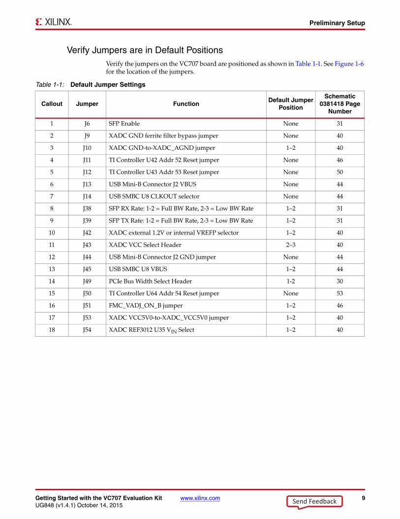
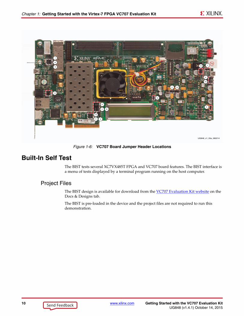
Verify Jumpers are in Default PositionsVerify the jumpers on the VC707 board are positioned as shown in Table 1-1. See Figure 1-6 for the location of the jumpers.
Table 1-1: Default Jumper Settings
Callout Jumper FunctionDefault Jumper
Position
Schematic 0381418 Page
Number
1 J6 SFP Enable None 31
2 J9 XADC GND ferrite filter bypass jumper None 40
3 J10 XADC GND-to-XADC_AGND jumper 1–2 40
4 J11 TI Controller U42 Addr 52 Reset jumper None 46
5 J12 TI Controller U43 Addr 53 Reset jumper None 50
6 J13 USB Mini-B Connector J2 VBUS None 44
7 J14 USB SMBC U8 CLKOUT selector None 44
8 J38 SFP RX Rate: 1-2 = Full BW Rate, 2-3 = Low BW Rate 1–2 31
9 J39 SFP TX Rate: 1-2 = Full BW Rate, 2-3 = Low BW Rate 1–2 31
10 J42 XADC external 1.2V or internal VREFP selector 1–2 40
11 J43 XADC VCC Select Header 2–3 40
12 J44 USB Mini-B Connector J2 GND jumper None 44
13 J45 USB SMBC U8 VBUS 1–2 44
14 J49 PCIe Bus Width Select Header 1-2 30
15 J50 TI Controller U64 Addr 54 Reset jumper None 53
16 J51 FMC_VADJ_ON_B jumper 1–2 46
17 J53 XADC VCC5V0-to-XADC_VCC5V0 jumper 1–2 40
18 J54 XADC REF3012 U35 VIN Select 1–2 40
Send Feedback
10 www.xilinx.com Getting Started with the VC707 Evaluation KitUG848 (v1.4.1) October 14, 2015
Chapter 1: Getting Started with the Virtex-7 FPGA VC707 Evaluation Kit
Built-In Self TestThe BIST tests several XC7VX485T FPGA and VC707 board features. The BIST interface is a menu of tests displayed by a terminal program running on the host computer.
Project FilesThe BIST design is available for download from the VC707 Evaluation Kit website on the Docs & Designs tab.
The BIST is pre-loaded in the device and the project files are not required to run this demonstration.
X-Ref Target - Figure 1-6
Figure 1-6: VC707 Board Jumper Header Locations
9
UG848_c1_05a_082214
1
8
14
511
10
6
12
23
4 15
17
18
16
713
Send Feedback
Getting Started with the VC707 Evaluation Kit www.xilinx.com 11UG848 (v1.4.1) October 14, 2015
Built-In Self Test
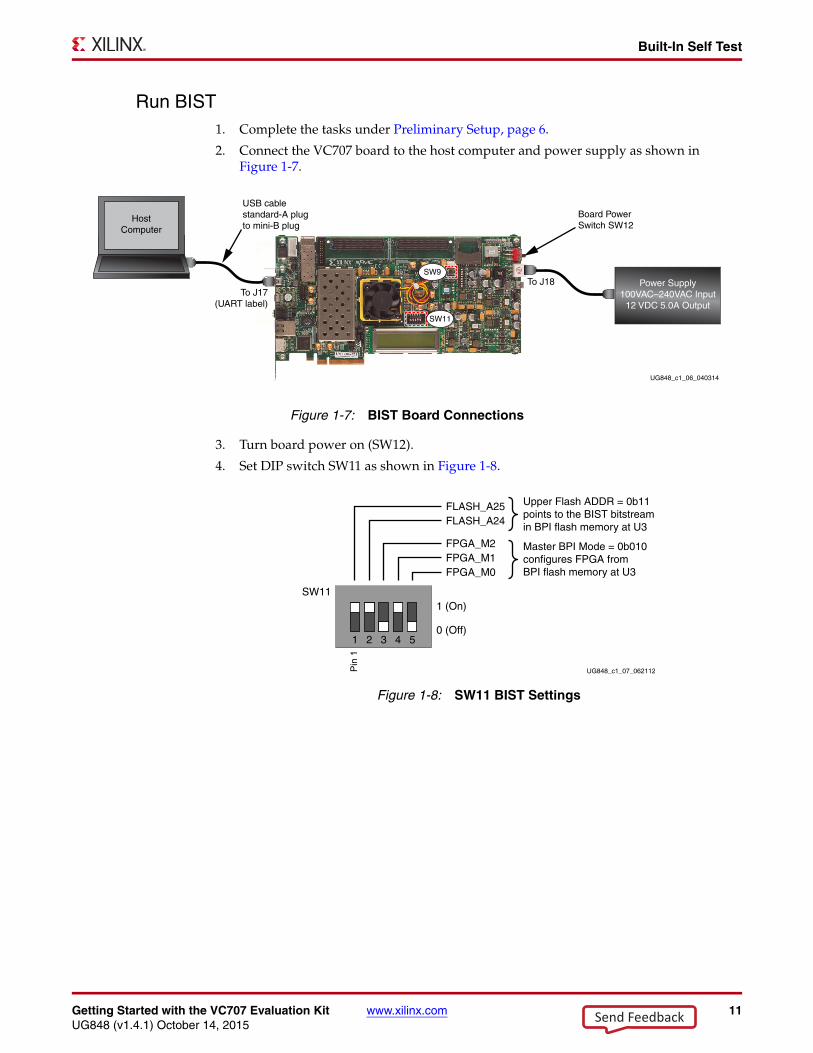
Run BIST1. Complete the tasks under Preliminary Setup, page 6.
2. Connect the VC707 board to the host computer and power supply as shown in Figure 1-7.
3. Turn board power on (SW12).
4. Set DIP switch SW11 as shown in Figure 1-8.
X-Ref Target - Figure 1-7
Figure 1-7: BIST Board Connections
UG848_c1_06_040314
Power Supply100VAC–240VAC Input
12 VDC 5.0A Output
To J18
Board PowerSwitch SW12
HostComputer
USB cablestandard-A plugto mini-B plug
SW11
To J17(UART label)
SW9
X-Ref Target - Figure 1-8
Figure 1-8: SW11 BIST Settings
UG848_c1_07_062112
SW11
1 2 3 4 5
FPGA_M0
0 (Off)
FPGA_M1FPGA_M2
FLASH_A24FLASH_A25
1 (On)
Pin
1
Upper Flash ADDR = 0b11points to the BIST bitstreamin BPI flash memory at U3
Master BPI Mode = 0b010configures FPGA fromBPI flash memory at U3
Send Feedback
12 www.xilinx.com Getting Started with the VC707 Evaluation KitUG848 (v1.4.1) October 14, 2015
Chapter 1: Getting Started with the Virtex-7 FPGA VC707 Evaluation Kit
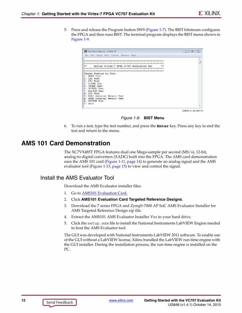
5. Press and release the Program button SW9 (Figure 1-7). The BIST bitstream configures the FPGA and then runs BIST. The terminal program displays the BIST menu shown in Figure 1-9.
6. To run a test, type the test number, and press the Enter key. Press any key to end the test and return to the menu.
AMS 101 Card DemonstrationThe XC7VX485T FPGA features dual one Mega-sample per second (MS/s), 12-bit, analog-to-digital converters (XADC) built into the FPGA. The AMS card demonstration uses the AMS 101 card (Figure 1-11, page 14) to generate an analog signal and the AMS evaluator tool (Figure 1-13, page 15) to view and control the signal.
Install the AMS Evaluator ToolDownload the AMS Evaluator installer files:
1. Go to AMS101 Evaluation Card.
2. Click AMS101 Evaluation Card Targeted Reference Designs.
3. Download the 7 series FPGA and Zynq®-7000 AP SoC AMS Evaluator Installer for AMS Targeted Reference Design zip file.
4. Extract the AMS101 AMS Evaluator Installer Vxx to your hard drive.
5. Click the setup.exe file to install the National Instruments LabVIEW Engine needed to host the AMS Evaluator tool.
The GUI was developed with National Instruments LabVIEW 2011 software. To enable use of the GUI without a LabVIEW license, Xilinx bundled the LabVIEW run-time engine with the GUI installer. During the installation process, the run-time engine is installed on the PC.
X-Ref Target - Figure 1-9
Figure 1-9: BIST Menu
UG848_c1_08_062112
Send Feedback
Getting Started with the VC707 Evaluation Kit www.xilinx.com 13UG848 (v1.4.1) October 14, 2015
AMS 101 Card Demonstration
Extract the AMS Design Files1. Go to the VC707 Evaluation Kit website and navigate to the Docs & Designs tab.
2. Click Virtex-7 FPGA VC707 Evaluation Kit.
3. Navigate to the software version that you are using, click + to expand the document type list, and click Targeted Reference Designs.
4. Download the “AMS Targeted Reference Design for Virtex-7 FPGA VC707 Evaluation Kit” zip file.
5. After downloading the design files, open the xadc_eval_design_vc707_vxx folder and unzip the files to a working directory on the host computer.
6. Open the ChipScope™ Pro Analyzer in the ISE design tools.
7. Click Open_cable.
8. Select Device, choose Configure, and click Select New File.
9. Open the AMS design in the xadc_eval_design_vc707_vxx folder by opening the ready_to_test folder and selecting the xadc_eval_design.bit file.
Set Up the Hardware1. Complete the tasks under Preliminary Setup, page 6.
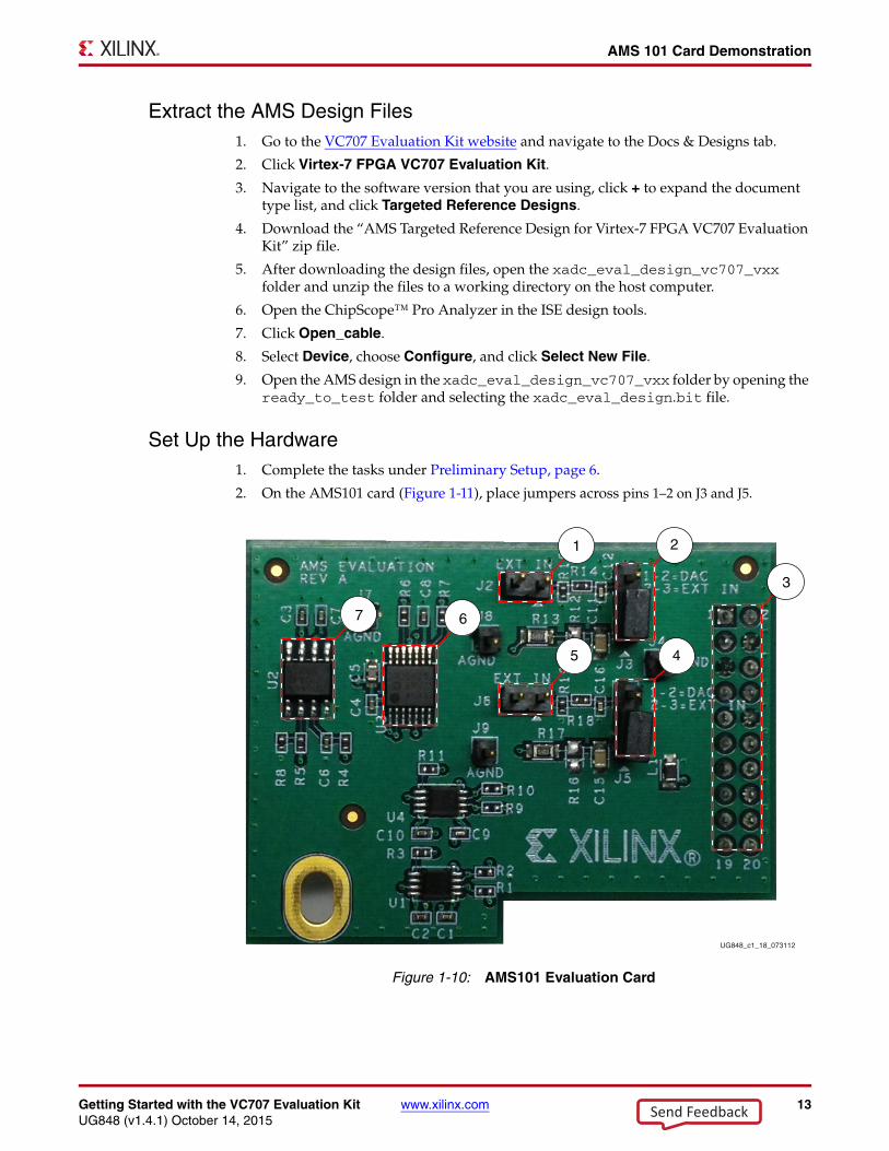
2. On the AMS101 card (Figure 1-11), place jumpers across pins 1–2 on J3 and J5.X-Ref Target - Figure 1-10
Figure 1-10: AMS101 Evaluation Card
UG848_c1_18_073112
1
2
3
67
45
2
Send Feedback
14 www.xilinx.com Getting Started with the VC707 Evaluation KitUG848 (v1.4.1) October 14, 2015
Chapter 1: Getting Started with the Virtex-7 FPGA VC707 Evaluation Kit
3. Turn off the VC707 board power (SW12) before installing the AMS 101 card on the VC707 board XADC header J35.
4. Plug the AMS 101 Card into the XADC header J35 on the VC707 board as shown in Figure 1-11.
5. Connect the VC707 board to the host computer and power supply as shown in Figure 1-11.
6. Turn board power on (SW12).
Examine Analog Mixed Signal FeaturesThe AMS evaluator tool (Figure 1-13) is useful for examining analog signals in the time and frequency domains, displaying linearity, viewing the XADC register settings, and monitoring the internal FPGA temperature sensor and supply voltages. The AMS evaluator tool also provides user-controllable decimation on the XADC output data to enhance the signal-to-noise ratio (SNR) performance.
Table 1-2: AMS101 Evaluation Card Jumper and Component Notes
CalloutReference Designator
Notes
1 J2 External signal source input to VP positive analog input.
2 J3 Jumper on pins 1–2 selects DAC signal source.Jumper on pins 2–3 selects external input source on J2.
3 20-pin connector to XADC header J35 on the VC707 board.
4 J5 Jumper on pins 1–2 selects DAC signal source.Jumper on pins 2–3 selects external input source on J6.
5 J6 External signal source to VN negative analog input.
6 U3 16-bit DAC. Sets analog test voltage.
7 U2 Reference buffer for DAC.
X-Ref Target - Figure 1-11
Figure 1-11: BIST Board Connections
UG848_c1_19_040314
Power Supply100VAC–240VAC Input
12 VDC 5.0A Output
To J18
Board PowerSwitch SW12
USB cablestandard-A plugto mini-B plug
To J17(UART)
HostComputer
USB cablestandard-A plugto micro-B plug
To JTAG
AMS 101 Evaluation Card
Send Feedback
Getting Started with the VC707 Evaluation Kit www.xilinx.com 15UG848 (v1.4.1) October 14, 2015
AMS 101 Card Demonstration
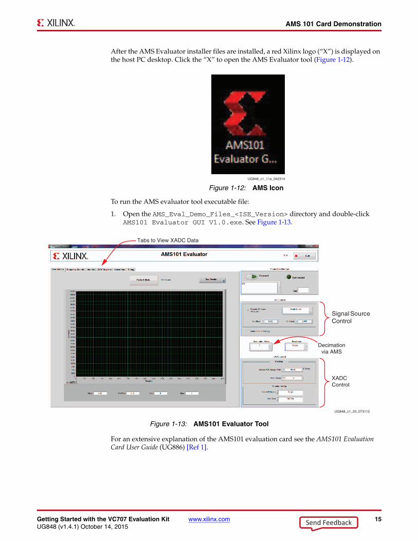
After the AMS Evaluator installer files are installed, a red Xilinx logo (“X”) is displayed on the host PC desktop. Click the “X” to open the AMS Evaluator tool (Figure 1-12).
To run the AMS evaluator tool executable file:
1. Open the AMS_Eval_Demo_Files_<ISE_Version> directory and double-click AMS101 Evaluator GUI V1.0.exe. See Figure 1-13.
For an extensive explanation of the AMS101 evaluation card see the AMS101 Evaluation Card User Guide (UG886) [Ref 1].
X-Ref Target - Figure 1-12
Figure 1-12: AMS IconUG848_c1_11a_042314
X-Ref Target - Figure 1-13
Figure 1-13: AMS101 Evaluator Tool
Tabs to View XADC Data
Signal SourceControl
Decimationvia AMS
XADCControl
UG848_c1_20_073112
Send Feedback
16 www.xilinx.com Getting Started with the VC707 Evaluation KitUG848 (v1.4.1) October 14, 2015
Chapter 1: Getting Started with the Virtex-7 FPGA VC707 Evaluation Kit
Next Steps1. Download the VC707 Evaluation Board for the Virtex-7 FPGA User Guide (UG885) [Ref 2].
2. Review and run the reference designs available at the VC707 Evaluation Kit website from the Docs & Designs tab.
Additional InformationVC707 board reference design files, user guides, schematics, and bill of materials, can be downloaded from the VC707 Evaluation Kit website.
Other documents associated with Xilinx devices, design tools, intellectual property, boards, and kits are available at the Xilinx documentation website.
Instructions for restoring the BPI flash memory with the factory-loaded reference designs are provided in VC707 Restoring Flash Contents (XTP145) [Ref 3].
For an extensive explanation of the AMS101 evaluation card, see the AMS101 Evaluation Card User Guide (UG886) [Ref 1].
Send Feedback
Getting Started with the VC707 Evaluation Kit www.xilinx.com 17UG848 (v1.4.1) October 14, 2015
Appendix A
VC707 Board Components
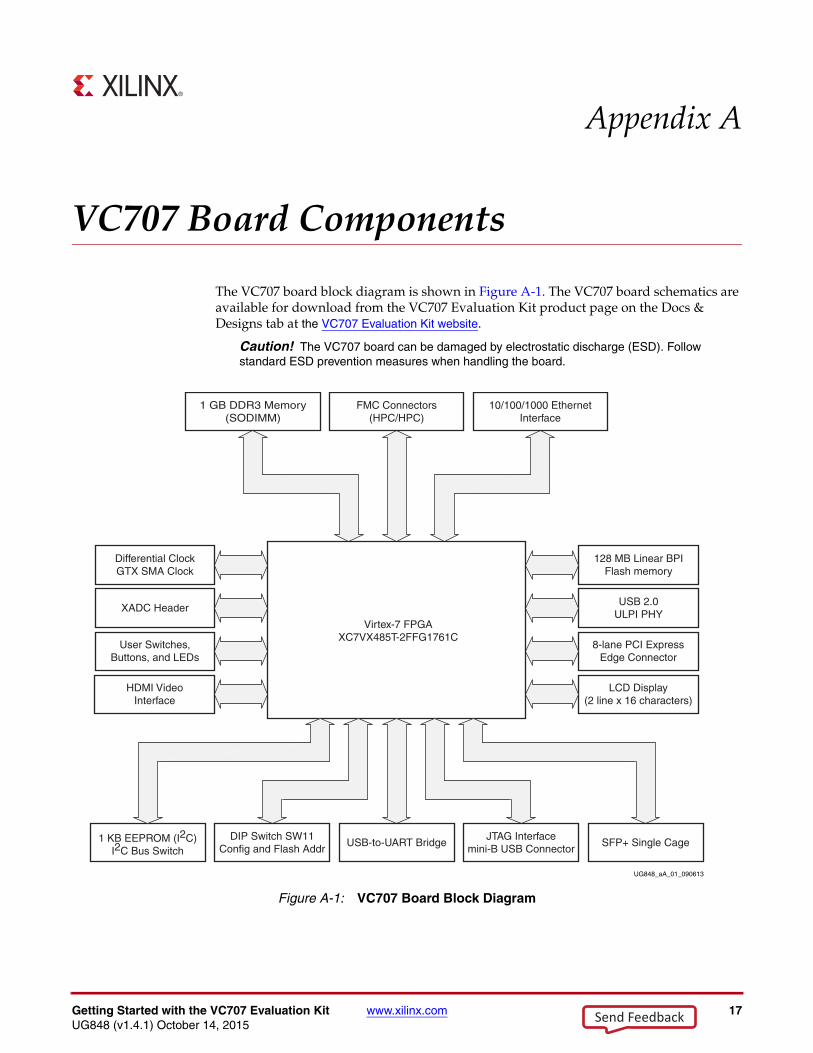
The VC707 board block diagram is shown in Figure A-1. The VC707 board schematics are available for download from the VC707 Evaluation Kit product page on the Docs & Designs tab at the VC707 Evaluation Kit website.
Caution! The VC707 board can be damaged by electrostatic discharge (ESD). Follow standard ESD prevention measures when handling the board.
X-Ref Target - Figure A-1
Figure A-1: VC707 Board Block Diagram
UG848_aA_01_090613
Virtex-7 FPGAXC7VX485T-2FFG1761C
128 MB Linear BPIFlash memory
USB 2.0ULPI PHY
8-lane PCI ExpressEdge Connector
LCD Display(2 line x 16 characters)
1 KB EEPROM (I2C)I2C Bus Switch
XADC Header
User Switches,Buttons, and LEDs
HDMI VideoInterface
Differential ClockGTX SMA Clock
1 GB DDR3 Memory(SODIMM)
FMC Connectors(HPC/HPC)
10/100/1000 EthernetInterface
DIP Switch SW11Config and Flash Addr
USB-to-UART BridgeJTAG Interface
mini-B USB ConnectorSFP+ Single Cage
Send Feedback
18 www.xilinx.com Getting Started with the VC707 Evaluation KitUG848 (v1.4.1) October 14, 2015
Appendix A: VC707 Board Components
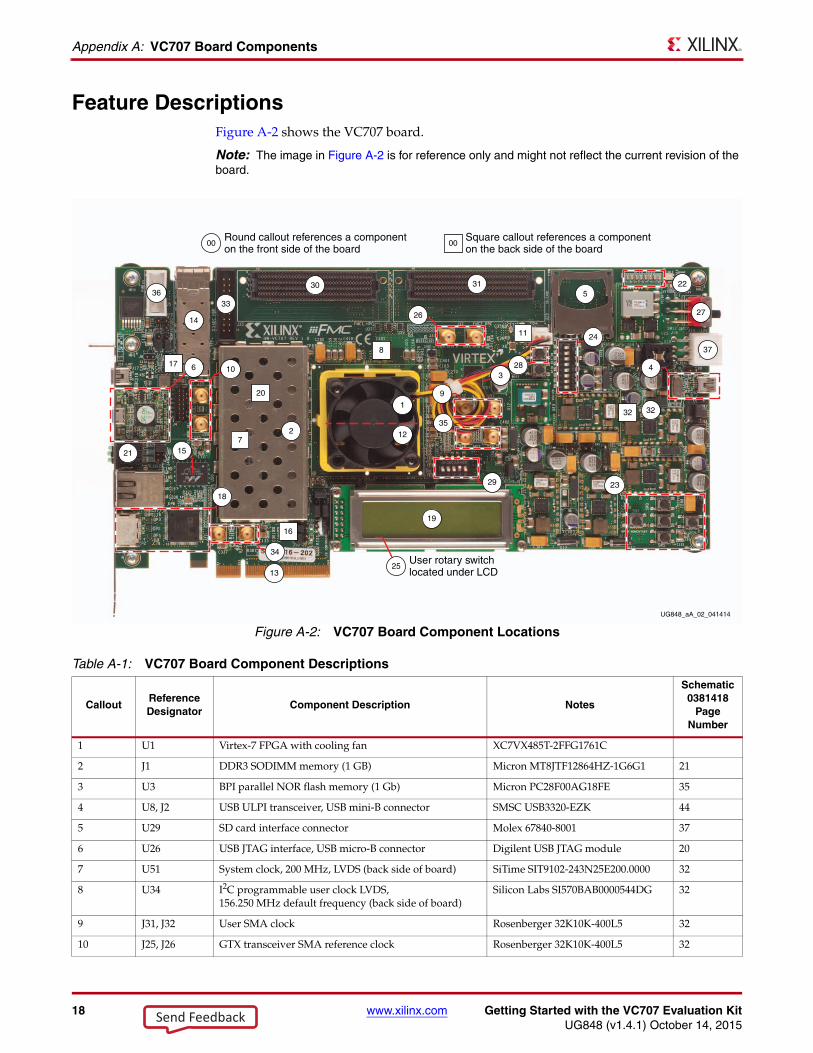
Feature DescriptionsFigure A-2 shows the VC707 board.
Note: The image in Figure A-2 is for reference only and might not reflect the current revision of the board.
X-Ref Target - Figure A-2
Figure A-2: VC707 Board Component Locations
30 31
33
21
32
26
35
34
32
27
19
22
24
23
User rotary switchlocated under LCD
25
20
28
29
18
13
15
16
27
617
14
1
8
12
103
9
11
5
4
00Square callout references a componenton the back side of the board
Round callout references a componenton the front side of the board
00
UG848_aA_02_041414
36
37
Table A-1: VC707 Board Component Descriptions
CalloutReference Designator
Component Description Notes
Schematic 0381418
Page Number
1 U1 Virtex-7 FPGA with cooling fan XC7VX485T-2FFG1761C
2 J1 DDR3 SODIMM memory (1 GB) Micron MT8JTF12864HZ-1G6G1 21
3 U3 BPI parallel NOR flash memory (1 Gb) Micron PC28F00AG18FE 35
4 U8, J2 USB ULPI transceiver, USB mini-B connector SMSC USB3320-EZK 44
5 U29 SD card interface connector Molex 67840-8001 37
6 U26 USB JTAG interface, USB micro-B connector Digilent USB JTAG module 20
7 U51 System clock, 200 MHz, LVDS (back side of board) SiTime SIT9102-243N25E200.0000 32
8 U34 I2C programmable user clock LVDS,156.250 MHz default frequency (back side of board)
Silicon Labs SI570BAB0000544DG 32
9 J31, J32 User SMA clock Rosenberger 32K10K-400L5 32
10 J25, J26 GTX transceiver SMA reference clock Rosenberger 32K10K-400L5 32
Send Feedback

Getting Started with the VC707 Evaluation Kit www.xilinx.com 19UG848 (v1.4.1) October 14, 2015
Feature Descriptions
11 U24 Jitter attenuated clock (back side of board) Silicon Labs SI5324C-C-GM 33
12 GTX transceiver Quad 111 – Quad 119 Embedded within FPGA U1 12 – 15
13 P1 PCI Express connector 8-lane card edge connector 30
14 P3 SFP/SFP+ module connector Molex 74441-0010 31
15 U50 10/100/1000 Mb/s Ethernet PHY Marvell M88E1111-BAB1C000 34
16 U2 SGMII GTX transceiver clock generator ICS ICS84402IAGI-01LF 32
17 U44 USB-to-UART bridge Silicon Labs CP2103GM 36
18 P2, U48 HDMI video connector, HDMI controller Molex 500254-1927, AD ADV7511KSTZ-P
43, 42
19 J23 LCD character display and connector 2 x 7 0.1 inch male header 39
20 U52 I2C Bus Switch (back side of board) TI PCA9548ARGER 41
21 DS11–DS13 Ethernet status LEDs EPHY status LED, dual green 34
22 DS2–DS9 User LEDs GPIO LEDs, green 0603 38
23 SW3–SW7 User pushbuttons, active-High E-Switch TL3301EP100QG 38
24 SW2 User DIP Switch 8-pole C and K SDA08H1SBD 38
25 SW10 User rotary switch (under LCD assembly) Panasonic EVQ-WK4001 38
26 J33, J34 User SMA GPIO Rosenberger 32K10K-400L5 32
27 SW12 Power on/off switch C&K 1201M2S3AQE2 45
28 SW9 FPGA PROG pushbutton E-Switch TL3301EP100QG 38
29 SW11 Config mode/upper linear flash address dip switch 5-pole C&K SDA05H1IBD 36
30 J35 FMC HPC1 connector (J35) Samtec ASP_134486_01 22–25
31 J37 FMC HPC2 connector (J37) Samtec ASP_134486_01 26–29
32 Power management system (front and back side of board)
TI UCD9248PFC in conjunction with various regulators
45–55
33 J19 Xilinx XADC header 2 x 10 0.1inch male header 40
34 J27, J28 GTX receiver SMA (RX) Rosenberger 32K10K-400L5 32
35 J29/J30 GTX transmitter SMA (TX) Rosenberger 32K10K-400L5 32
36 J5 2 x 5 shrouded PMBus connector Assmann HW10G-0202 46
37 J18 12V power input 2 x 3 connector Molex 39-30-1060 46
Table A-1: VC707 Board Component Descriptions (Cont’d)
CalloutReference Designator
Component Description Notes
Schematic 0381418
Page Number
Send Feedback
20 www.xilinx.com Getting Started with the VC707 Evaluation KitUG848 (v1.4.1) October 14, 2015
Appendix A: VC707 Board Components
Send Feedback
Getting Started with the VC707 Evaluation Kit www.xilinx.com 21UG848 (v1.4.1) October 14, 2015
Appendix B
Additional Resources
Xilinx ResourcesFor support resources such as Answers, Documentation, Downloads, and Forums, see the Xilinx Support website.
For continual updates, add the Answer Record to your myAlerts.
Solution CentersSee the Xilinx Solution Centers for support on devices, software tools, and intellectual property at all stages of the design cycle. Topics include design assistance, advisories, and troubleshooting tips.
ReferencesThe most up to date information related to the VC707 board and its documentation is available on these websites:
Virtex-7 VC707 Evaluation Kit
Virtex-7 VC707 Evaluation Kit documentation
Virtex-7 VC707 Evaluation Kit Master Answer Record (AR 45382)
These documents and sites provide supplemental material useful with this guide:
1. AMS101 Evaluation Card User Guide (UG886)2. VC707 Evaluation Board for the Virtex-7 FPGA User Guide (UG885)
3. VC707 Restoring Flash Contents (XTP145)
4. Silicon Labs
5. LogMeTT
6. National Instruments LabVIEW 32-bit Run-Time Engine
Send Feedback
22 www.xilinx.com Getting Started with the VC707 Evaluation KitUG848 (v1.4.1) October 14, 2015
Appendix B: Additional Resources
Send Feedback
Getting Started with the VC707 Evaluation Kit www.xilinx.com 23UG848 (v1.4.1) October 14, 2015
Appendix C
Warranty
THIS LIMITED WARRANTY applies solely to standard hardware development boards and standard hardware programming cables manufactured by or on behalf of Xilinx (“Development Systems”). Subject to the limitations herein, Xilinx warrants that Development Systems, when delivered by Xilinx or its authorized distributor, for ninety (90) days following the delivery date, will be free from defects in material and workmanship and will substantially conform to Xilinx publicly available specifications for such products in effect at the time of delivery. This limited warranty excludes: (i) engineering samples or beta versions of Development Systems (which are provided “AS IS” without warranty); (ii) design defects or errors known as “errata”; (iii) Development Systems procured through unauthorized third parties; and (iv) Development Systems that have been subject to misuse, mishandling, accident, alteration, neglect, unauthorized repair or installation. Furthermore, this limited warranty shall not apply to the use of covered products in an application or environment that is not within Xilinx specifications or in the event of any act, error, neglect or default of Customer. For any breach by Xilinx of this limited warranty, the exclusive remedy of Customer and the sole liability of Xilinx shall be, at the option of Xilinx, to replace or repair the affected products, or to refund to Customer the price of the affected products. The availability of replacement products is subject to product discontinuation policies at Xilinx. Customer may not return product without first obtaining a customer return material authorization (RMA) number from Xilinx.
THE WARRANTIES SET FORTH HEREIN ARE EXCLUSIVE. XILINX DISCLAIMS ALL OTHER WARRANTIES, WHETHER EXPRESS, IMPLIED OR STATUTORY, INCLUDING, WITHOUT LIMITATION, ANY WARRANTY OF MERCHANTABILITY, FITNESS FOR A PARTICULAR PURPOSE, OR NON-INFRINGEMENT, AND ANY WARRANTY THAT MAY ARISE FROM COURSE OF DEALING, COURSE OF PERFORMANCE, OR USAGE OF TRADE. (2008.10)
Do not throw Xilinx products marked with the “crossed out wheeled bin” in the trash. Directive 2002/96/EC on waste electrical and electronic equipment (WEEE) requires the separate collection of WEEE. Your cooperation is essential in ensuring the proper management of WEEE and the protection of the environment and human health from potential effects arising from the presence of hazardous substances in WEEE. Return the marked products to Xilinx for proper disposal. Further information and instructions for free-of-charge return available at the Waste Electrical and Electronic Equipment Program.
Send Feedback