Embed Size (px)
Citation preview
GROWTH AND CHARACTERIZATION OF III-V COMPOUNDSEMICONDUCTOR NANOSTRUCTURES BY METALORGANIC
CHEMICAL VAPOR DEPOSITION
BY
RYAN STEWART DOWDY
THESIS
Submitted in partial fulfillment of the requirementsfor the degree of Master of Science in Electrical and Computer Engineering
in the Graduate College of theUniversity of Illinois at Urbana-Champaign, 2009
Urbana, Illinois
Adviser:
Assistant Professor Xiuling Li
ii
ABSTRACT
Planar <110> GaAs nanowires and quantum dots grown by atmospheric MOCVD have
been introduced to non-standard growth conditions such as incorporating Zn and growing them
on free-standing suspended films and on 10° off-cut substrates. Zn doped nanowires exhibited
periodic notching along the axis of the wire that is dependent on Zn/Ga gas phase molar ratios.
Planar nanowires grown on suspended thin films give insight into the mobility of the seed
particle and change in growth direction. Nanowires that were grown on the off-cut sample
exhibit anti-parallel growth direction changes. Quantum dots are grown on suspended thin films
and show preferential growth at certain temperatures. Envisioned nanowire applications include
twin-plane superlattices, axial pn-junctions, nanowire lasers, and the modulation of nanowire
growth direction against an impeding barrier and varying substrate conditions.

iii
To my mother, father, and sister
iv
TABLE OF CONTENTS
1. Introduction ..................................................................................................................................1
2. Experimental Details ....................................................................................................................9
3. Vapor-Liquid-Solid Nanowires .................................................................................................15
4. Quantum Dots ............................................................................................................................33
5. Conclusion .................................................................................................................................43
1
1. INTRODUCTION
1.1 Compound Semiconductors
Compound semiconductors are a very versatile class of semiconductors. Typically
formed from periodic elements from groups III and V, or II and VI, they provide material
properties that are useful for a number of electrical and optical devices. They provide such
advantages as a direct bandgap, enhanced carrier mobility and the creation of ternary and
quaternary materials that have fine-tunable electronic and optical properties based on material
composition. This also allows the creation of functionalized layers that can be utilized in other
ways, such as utilizing specialized growth phenomena, sacrificial layers and strained layers
which are of use to create novel nanostructures such as semiconductor nanotubes [1], III-V
semiconductor nanowires [2], and self assembled III-V quantum dots [3]. This research focuses
mainly on nanostructures consisting of III-V semiconductor materials.
1.2 Crystal Structure
III-V materials are comprised of at least two different atoms that sit on a crystal
lattice. III-V crystal structures can occupy different crystal structures, two of the most common
polytypes being wurtzite and zinc-blende. Wurtzite is a hexagonal crystal structure with
alternating atoms (unlike simple hexagonal close-packed, which has alternating uni-atomic
layers) that follow an ABAB alternating layer structure, while the zinc-blende structure
resembles a normal cubic lattice but with a diatomic basis resulting in a structure that resembles
two BCC crystals interlaced with each other with an ABCABC layer structure. Since both zinc-
blende and wurtzite crystal structures of III-V materials have a diatomic basis, resulting in
2
alternating layers of material, they are prone to crystal defects. One of the main defect types is
the stacking fault. For example, in wurtzite a stacking fault would be ABABBA, where the two
B layers sit on top of each other instead of alternating between A and B. A special type of
stacking default that can occur in zinc-blende crystals (but not in wurtzite due to its mere 2
layers) is a twin defect, in which the crystal layers reverse order after a stacking fault. For
example, a twin defect would be ABCABCBACBA, where the original crystal order was ABC
but shifted to CBA. Polytypism is another type of growth phenomena where the crystal structure
changes, such as shifting from zinc-blende to wurtzite.
In the case of crystal growth, growth of polar semiconductor materials on single crystal
elemental semiconductor substrates can be problematic. Polar crystals, crystals with a diatomic
basis that results in differently charged atoms, behave differently than elemental crystals (such as
Si and Ge). Polar crystal grown on elemental crystal are usually wrought with defects called anti-
phase domains. Anti-phase domains occur when there is a monoatomic step on the surface of the
substrate and the deposited crystal is of a different crystal structure (i.e., zinc-blende structure on
a Si substrate) [4]. The step causes two like atoms to bond together, instead of two dissimilar
atoms. For example, normally GaAs bonds with Ga-As atoms, where an anti-phase domain
would bond Ga-Ga due to a monoatomic step on the Si substrate, hence causing a defect.
When growing heteroepitaxial crystals, the effects of strain should be considered. The
atoms in a crystal like to situate themselves at specific distances from one another. This bond
length dictates the length of the unit cell, the repeated atomic structure throughout a crystal,
which is also referred to as the lattice constant. In heteroepitaxy, when materials are deposited on
a substrate with a different lattice constant, there is a strain that is induced. If the material grown
has a larger lattice constant, the grown crystal is compacted and a compressive strain is created.
3
Suppose the crystal grown has a smaller lattice constant; then the atoms are pulled apart to
accommodate the substrate, forming a tensile strain. If the strain is too high, the bonds will break
and dislocations will form a metamorphic layer. Induced strain can also influence the bandgap of
crystals by adjusting the interatomic spacing. Compressive strain will cause the bandgap to
widen, as well as lifting the heavy hole band above the light hole band in the valance band.
Tensile strain shrinks the bandgap with the light hole band, raising it above the heavy hole band.
Strain can also influence the effective mass by altering the curvature of the band edges. Crystal
defects and strain are major concerns for III-V crystal growth on elemental crystal
substrates. The polyatomic nature of compound materials gives rise to issues that affect both
crystal growth as well as electronic and optical properties which will be further expounded upon.
1.3 Electrical Properties
In relation to semiconductor physics, some III-V semiconductors have phenomena
occurring that are not present in elemental semiconductors. Using GaAs, for example, phonons
are a contributing source of carrier scattering. When phonons, acoustic or optical, propagate
through the crystal lattice, they distort the lattice and create a deformation potential by locally
changing the band structure through changing the inter-atomic spacing of the crystal. In
polar crystals, the lattice can also be distorted by a charged carrier moving through the crystal
distorting a lattice; this is called a polaron. Due to the symmetrical nature and high curvature
(low electron effective mass) of the GaAs conduction band minimum, electrons are unaffected
by optical deformation potential scattering and resistant to acoustic phonon scattering. This leads
to a high electron mobility which can be utilized to create high speed devices that are difficult to
realize in elemental semiconductors. Unfortunately, the high electron mobility usually leads to a
4
disparity between electron and hole mobility, which is generally considered detrimental for
CMOS technologies. Improving hole mobility has been an active area of research in the field of
III-V electronic devices [5].
1.4 Optical Properties
III-V semiconductors have an important optical feature that distinguishes them from
elemental semiconductors: the direct band gap. In elemental semiconductor, Si or Ge, the
conduction band minima and valence band maxima do not share the same point in k-space. This
means that for an electron in the conduction band to radiatively recombine with a hole in the
valance band, it needs a shift in momentum to allow this to occur. Usually the source of
momentum change is a phonon to assist it, so radiative recombination in indirect materials is
limited by the availability of suitable phonons for light emission. This holds true for absorption
processes. Much of light conversion efficiency is lost in indirect materials due to non-radiative
recombination such as the Auger effect or phonon emission [6]. With direct bandgap
semiconductors, there is no intermediate step and they have much higher light conversion
efficiencies, making them choice materials for optical devices. Also, utilizing ternary and
quaternary compounds allows engineers to adjust the bandgap of materials to alter their
absorption/emission spectra according to the application of the device. Polar crystals also exhibit
special types of optical phonons, where two atoms vibrate against each other at high frequency
due to coloumbic effects between the crystals, called polar optical phonons. These phonons
couple readily with light, producing a new quasi particle—the polariton—which has been
investigated by researchers for new potentials in optical devices [7].
5
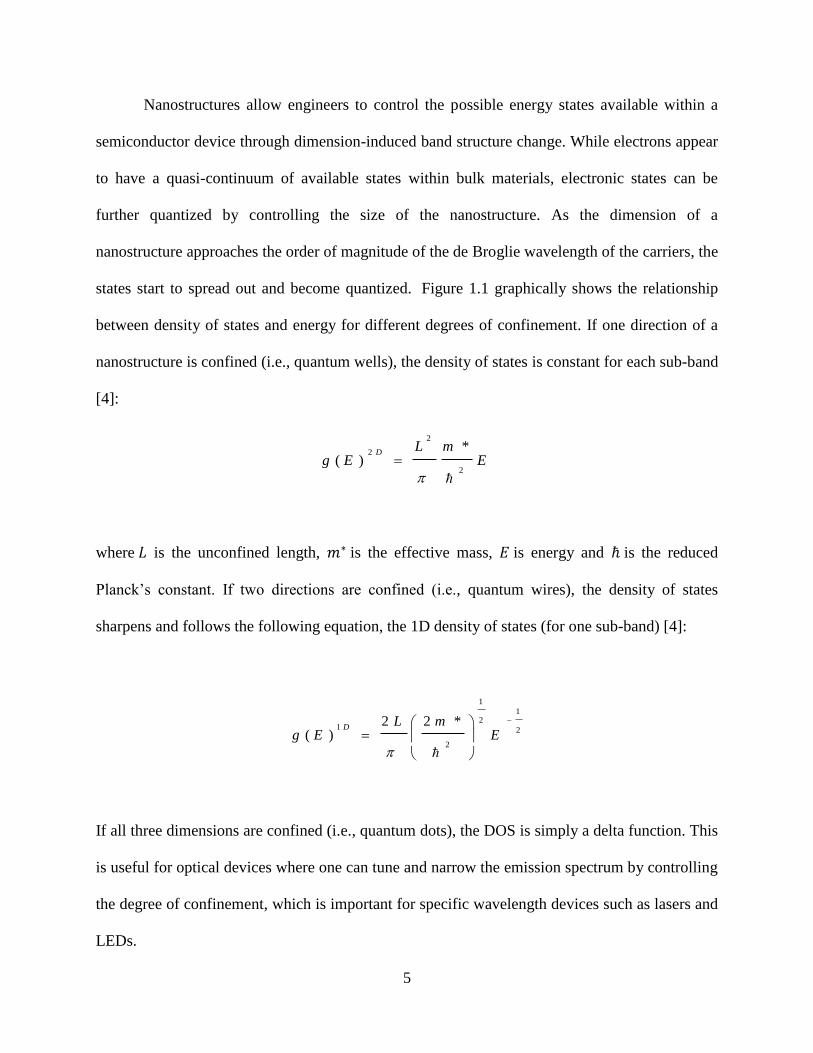
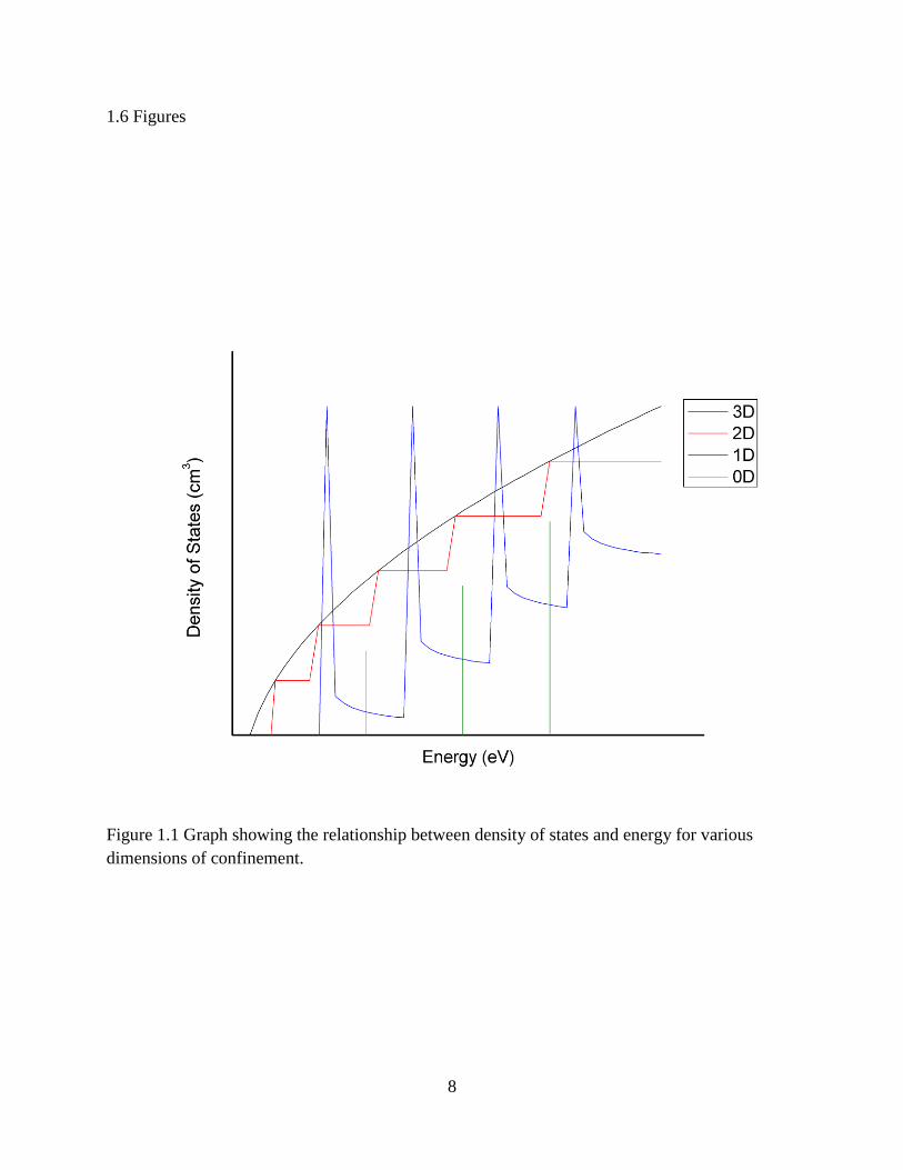
Nanostructures allow engineers to control the possible energy states available within a
semiconductor device through dimension-induced band structure change. While electrons appear
to have a quasi-continuum of available states within bulk materials, electronic states can be
further quantized by controlling the size of the nanostructure. As the dimension of a
nanostructure approaches the order of magnitude of the de Broglie wavelength of the carriers, the
states start to spread out and become quantized. Figure 1.1 graphically shows the relationship
between density of states and energy for different degrees of confinement. If one direction of a
nanostructure is confined (i.e., quantum wells), the density of states is constant for each sub-band
[4]:
EmL
EgD
2
2
2*
)(
where is the unconfined length, is the effective mass, is energy and is the reduced
Planck’s constant. If two directions are confined (i.e., quantum wires), the density of states
sharpens and follows the following equation, the 1D density of states (for one sub-band) [4]:
2
12
1
2
1*22
)(
E
mLEg
D
If all three dimensions are confined (i.e., quantum dots), the DOS is simply a delta function. This
is useful for optical devices where one can tune and narrow the emission spectrum by controlling
the degree of confinement, which is important for specific wavelength devices such as lasers and
LEDs.
6
While III-V nanostructures are a heavily researched field, there is still much to learn and
improve upon. Dopant and isoelectronic impurity incorporation in III-V VLS nanowires is still
under heavy investigation. Researchers are still unsure about whether the impurities diffuse
through the nanowires or into the colloid itself. Planar nanowires have a distinct feature in which
they interact heavily with the substrate along their entire length. Placing them in scenarios with
alternating substrates may prove beneficial to understanding their intricate nature. The growth of
III-V on silicon has been an age-old problem for crystal growers. Growth on suspended silicon
membranes may play an important role in solving this dilemma, as well aid in the process of
ordering quantum dots without the need for lithography. This work intends to tackle and shed
light on these topics.
1.5 References
[1] C. Ik Su and L. Xiuling, "Controlled assembly and dispersion of strain-induced
InGaAs/GaAs nanotubes," IEEE Transactions on Nanotechnology, vol. 7, pp. 493-495,
July 2008.
[2] S. A. Fortuna, J. Wen, I. S. Chun, and X. Li, "Planar GaAs nanowires on GaAs (100)
substrates: Self-aligned, nearly twin-defect free, and transfer-printable," Nano Letters,
vol. 8, pp. 4421-4427, Nov. 2008.
[3] P. M. Petroff and S. P. DenBaars, "MBE and MOCVD growth and properties of self-
assembling quantum dot arrays in III-V semiconductor structures," Superlattices and
Microstructures, vol. 15, p. 15, Aug. 1994.
[4] M. Grundmann, The Physics of Semiconductors: An Introduction Including Devices and
Nanophysics. New York, NY: Springer-Verlag, 2006.
[5] O. InJo, H. Kim, M. Zhang, T. Lee, F. Zhu, L. Yu, S. Koveshnikov, W. Tsai, V.
Tokranov, M. Yakimov, S. Oktyabrsky, and J. C. Lee, "Self-aligned n- and p-channel
GaAs MOSFETs on undoped and p-type substrates using HfO2 and silicon interface
passivation layer," in International Electron Devices Meeting, 2006, pp. 1-4.
[6] J. I. Pankove, Optical Processes in Semiconductors. New York, NY: Dover, 1975.
7
[7] S. I. Tsintzos, N. T. Pelekanos, G. Konstantinidis, Z. Hatzopoulos, and P. G. Savvidis, "A
GaAs polariton light-emitting diode operating near room temperature," Nature, vol. 453,
pp. 372-375, 2008.
8
1.6 Figures
Figure 1.1 Graph showing the relationship between density of states and energy for various
dimensions of confinement.
9
2. EXPERIMENTAL DETAILS
2.1 Metalorganic Chemical Vapor Deposition
Metalorganic chemical vapor deposition (MOCVD) is a specialized form of CVD that is
used to deposit epitaxial films. Typically MOCVD is used to deposit compound semiconductors,
but it can also be used to deposit elemental semiconductors such as silicon and germanium.
Compound semiconductors grown by MOCVD offer a wide variety of benefits such as
adjustable material composition, in situ doping of grown layers and faster growth rates than other
deposition techniques like molecular beam epitaxy (MBE). Film deposition is produced by
flowing in a metalorganic precursor such as trimethylgallium (TMGa) for gallium. or
trimethylindium (TMI) for indium, and a hydride such as arsine (AsH3) for arsenic or
phosphine (PH3) for phosphorous, into a reactor chamber. High purity hydrogen (H2) and
sometimes nitrogen (N2) gas are commonly used as carrier gas. The precursor molecules
pyrolyse, or crack, under high temperature and deposit the desired material on the surface of the
sample while the gaseous byproduct and unreacted precursors are swept to the exhaust. Dopant
precursors can be flown during crystal growth to form doped epitaxial films. Dopants can either
be incorporated through a metalorganic source, such as dimethyl zinc (DMZn) or a hydride
source such as silane (SiH4) or disilane (Si2H6). An interesting phenomenon occurs in III-V
materials when doping is considered. Since they contain atoms from both group III and group V,
their dopants can behave amphoterically. This means that the dopants can either behave as n-type
dopants or p-type dopants depending on which lattice site they sit on. Usually the dopant type,
growth temperature and other growth conditions dictate how the dopant behaves.
10
In thin film epitaxy there are three growth mods that govern crystal epitaxy depending on
growth conditions [1]. The first growth mode occurs when films are relatively lattice-matched
and are comparable. As adatoms attach to the surface they form a very thin wetting layer. This
thin layer forms evenly on the surface, forming a high quality thin epitaxial film. This growth
mode is called layer-by-layer growth, or Frank van der Merwe growth mode. The second growth
mode, Volmer-Weber growth, is the formation of large islands of crystal, usually metamorphic.
This growth mode is achieved either when adatoms prefer to aggregate with each other instead of
attaching to the substrate, or when strain interaction is too high with the substrate and formation
with other adatoms is preferential. This resulting growth is usually entirely 3D, riddled with
dislocations and defects at the growth interface. Lastly, the third growth mode is a combination
of the first two, when the thin wetting layer forms but adatoms merge to form a 3D growth on
top of an often psuedomorphic 2D wetting layer. This growth mode, Stranski-Krastinov, is
highly desirable in the formation of nanostructures, especially quantum dots. This allows for the
benefit of a 3D structure with the high quality interface of a 2D epitaxial film.
2.2 Vapor-Liquid-Solid Growth
In 1964, Wagner and Ellis [2] discovered a method to create such 1D structures via CVD
growth. These whiskers (now commonly referred to as nanowires) were fabricated by a
mechanism called vapor-liquid-solid growth. Metal is deposited onto the surface of a single
crystalline semiconductor by evaporation, sputtering or in colloid form. A liquid metal particle
forms between the metal and the semiconductor when the substrate is heated above the eutectic
temperature of the alloy. A vapor phase precursor is introduced into the reactor, decomposes on
the surface of the particle, and diffuses inward. Once the particle becomes super-saturated and a
11
single-crystalline solid is precipitated out the particle. This results in an extremely anisotropic
nanowire with well-defined crystal facets and a diameter that is dependent on the size of the
particle.
Usually, nanowires are grown in non-planar directions with the <111> direction being
one of the most common. The issue with non-planar wires is that they are hard to integrate with
traditional planar devices (CMOS, optoelectronics) without removing them from their host
substrate. Interestingly enough, under the right growth conditions, planar nanowires can be
grown epitaxially on the surface; <110> GaAs nanowires can be grown planar on <100> GaAs
substrates. While nanowires have been researched extensively for the last decade, planar GaAs
nanowires still have to be fully characterized since the controlled growth of planar nanowires
was first reported by our research group in 2008 [3]. This work discusses some of the efforts to
characterize the effect of Zn doping, In incorporation, suspended thin membranes and off-cut
substrate growth of <110> planar GaAs nanowires.
Planar <110> GaAs nanowires are grown by in a Thomas Swan atmospheric MOCVD
reactor. The MOCVD reactor is a vertical setup utilizing a quartz chamber, with a graphite
susceptor that is heated via an RF generator and growth substrates are (100) semi-insulating
GaAs. Trimethylgallium (TMGa) and trimethylindium (TMI) are used as the group III sources
while AsH3 is used as the group V hydride and diethylzinc (DEZn) is utilized as the Zn source.
H2 is used as the carrier gas. Au colloid, with sizes ranging from 20 to 250 nm, suspended in an
aqueous solution is deposited on epi-ready (100) semi-insulating GaAs wafers. Excess water is
removed through evaporation by simply heating the sample on a 115 C° hotplate. To create
suspended films, 50 nm of GaAs are grown on top of 1 μm of Al.75Ga.25As on GaAs substrate.
Bowtie shaped patterns are used to create an area of suspended and supported GaAs for nanowire
12
synthesis to occur. The lithography pattern is transferred to the GaAs by a 1:8:80
H2SO4:H2O2:H2O etch, and then the sacrificial Al.75Ga.25As layer is removed by a 49% HF etch.
For the suspended structures, Au is deposited prior to lithography and wet chemical etching for
two reasons: (1) to prevent stiction [4] and damage to the suspended film due to the drying action
of the Au colloid solution and (2) to reduce variability of Au colloid density across the sample by
having some colloid naturally rinsed away during processing.
Before metalorganics are flowed, the samples are heated to 625 C° in situ for 10 min in
the presence of AsH3 (to prevent arsenic desorption from the substrate) in order to remove the
native oxide and anneal the gold colloid before growth. With the suspended film, wires are
grown at 460 °C with a targeted growth rate of 43 nm/s. The control flow rates are 10 sccm of
TMGa with AsH3 ranging from 200 sccm during the oxide desorption step and increased to 500
sccm during the actual growth. For the impurity effect tests, molar flow ratios of impurity to
TMGa range from 8.0 x 10⁻⁵
to 2.0 x 10⁻²
. The wires are first grown halfway for 70 s with just
TMGa and AsH3 present, then after a 15 s pause the impurities are flown with TMGa for another
70 s. After growth, the samples are cooled in the presence of AsH3 for 5 min. Nanowires were
characterized post growth by a Hitachi S4800 scanning electron microscope (SEM) and 15 kV at
also with a JEOL 2010 LaB6 transmission electron microscope (TEM).
2.3 Preparation of Silicon Membranes and Quantum Dot Growth.
The growth of III-V self-assembled quantum dots on thin silicon suspended membranes
is a two-step process. The substrate is a silicon-on-insulator wafer supplied by Soitec and
provided to us by Max Lagally’s group at the University of Wisconsin at Madison. The
manufacturing process of SOI wafers can be viewed at the Soitec web site [5]. For our
13
experiments, the thickness of the silicon active layer is 25 nm or 13 nm. A pattern of various
squares sized 20 x 20 μm2, 10 x 10 μm
2, 5 x 5 μm
2 and 2 x 2 μm
2 are formed via
photolithography followed by reactive ion etching. Photoresist is then stripped and thoroughly
cleaned by degreasing using a combination of acetone, methanol and isopropyl alcohol to
remove any organic materials. The suspended edge is created by using the buried oxide as a
sacrificial layer to undercut the silicon on top of the insulator. A dilute 1:10 HF:H2O is used for
15 min in order to create a proper undercut. The undercut is around 1 µm from each edge of the
square pattern, with the 2 x 2 μm2 squares being removed as an indicator of proper etching. The
samples are dried then loaded into the MOCVD reactor chamber to begin growth.
The Thomas Swan atmospheric MOCVD reactor is used for quantum dot growth as well.
The samples are prepared the same way as nanowire samples except that AsH3 is not flown
during the desorption step as there is no concern for arsenic desorption for a silicon substrate.
TMGa is used as the gallium precursor and AsH3 as the hydride source. The nominal growth
temperature is 450 Co during the deposition of the quantum dots and is maintained during the
growth interruption. The nominal time for the growth interruption is 30 s; during this time AsH3
is switched off with only carrier gas flowing to prevent hydrogen incorporation into the quantum
dots [6], and to allow their proper formation. After the growth interruption, AsH3 is switched
back on and the temperature is cooled down to ambient. The dots are then characterized by SEM
in a Hitachi S4800 scanning electron microscope. Correlations between growth conditions and
quantum dot results are discussed further in the quantum dot chapter in this work.
2.4 References
[1] J. A. Venables, G. D. T. Spiller, and M. Hanbucken, "Nucleation and growth of thin
films," Reports on Progress in Physics, vol. 47, pp. 399-459, Apr. 1984.
14
[2] R. S. Wagner and W. C. Ellis, "Vapor-liquid-solid mechanism of single crystal growth,"
Applied Physics Letters, vol. 4, pp. 89-90, Mar. 1964.
[3] S. A. Fortuna, J. Wen, I. S. Chun, and X. Li, "Planar GaAs nanowires on GaAs (100)
substrates: Self-aligned, nearly twin-defect free, and transfer-printable," Nano Letters,
vol. 8, pp. 4421-4427, Nov. 2008.
[4] N. Tas, T. Sonnenberg, H. Jansen, R. Legtenberg, and M. Elwenspoek, "Stiction in
surface micromachining," Journal of Micromechanics and Microengineering, vol. 6, pp.
385–397, Dec. 1996.
[5] "Soitec - Smart Cut™, Smart Choice." [Online] Available: http://www.soitec.com
/en/technology/smart-cut-smart-choice.php
[6] F. Heinrichsdorff, A. Krost, D. Bimberg, A. O. Kosogov, and P. Werner, "Self organized
defect free InAs/GaAs and InAs/InGaAs/GaAs quantum dots with high lateral density
grown by MOCVD," Applied Surface Science, vol. 123-124, pp. 725-728, Jan. 1998.
15
3. VAPOR-LIQUID-SOLID NANOWIRES
3.1 Zinc Perturbation of Planar Nanowire Growth
Zinc is an important p-type dopant in gallium arsenide based III-V semiconductors. It is a
non amphoteric dopant (unlike silicon), does not have the etching issue of carbon tetrabromide
[1] and is readily available in its metalorganic form (DEZn or dimethylzinc (DMZn)). It does
have its drawbacks as zinc is also known for being highly diffusive [2] in epitaxial GaAs films.
In order to create electronic and photonic nanowire devices, understanding the mechanism
behind how Zn is incorporated in VLS nanowires is essential. Zinc implantation [3] and in situ
incorporation of zinc in vertical <111> nanowires [4] have been investigated. It has been
confirmed recently that Zn incorporates through the metal catalyst in GaAs VLS nanowires [4].
It was also found that at certain precursor levels Zn encourages the formation of zinc-blende (in
contrast to wurtzite) InP nanowires [5]. This phenomenon was used to create periodic twinning
structures in nanowires at Zn incorporation levels above 1e18 cm-3
.
To illustrate the effect of Zn incorporation in our planar nanowire growth, a two-step
growth scheme is used, starting with a Zn-free growth segment followed by turning on the DEZn
source while keeping all other growth conditions constant. Figure 3.1 displays SEM images of
Zn-doped GaAs growth effects as a function of Zn doping concentration. Clearly, without the
presence of Zn, our planar nanowire growth condition favors the <110> orientation in the plane
of (100), and extends the zinc-blende structure of the substrate epitaxially in the axial direction,
as reported previously [6]. At Zn/Ga gas phase molar ratios above 0.8% (3.6e19 cm-3
), nanowires
immediately deviate from their planar growth trajectory and take off in directions that seem
random but twist back and forth around <111> (Figure 3.1a). No wires remain planar as soon as
16
DEZn is switched on above this molar ratio. This implies that Zn incorporation at this level
lowers the formation energy of non-<110> growth orientations, particularly the <111> solid-
liquid interface, and thus steers the growth orientation off the <110> path. When the Zn/Ga ratio
is lowered by an order of magnitude to 0.08% (3.6e18 cm-3
), nanowire growth remains planar
(Figure 3.1d) but exhibits characteristic “periodic notching” along the surface of the nanowire
and side facets. We also have found that the period length between notches is on the same order
of magnitude (~.91x) as the seed particle size, as shown in Figure 3.2, which suggests that the
notching period is controllable depending on the seed particle size chosen. In addition to the
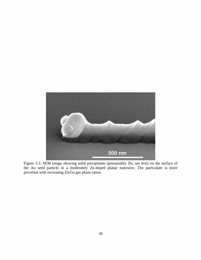
notching, some solid precipitants have been observed on the surface of the Au colloid, as shown
in Figure 3.3; these are more prevalent in the 0.08% Zn/Ga molar ratio, implying that the
precipitates could be Zn rich.
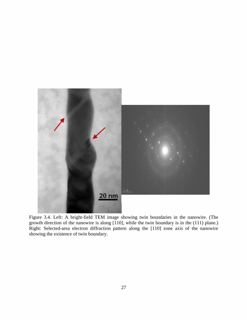
To better understand the mechanism of the “notching” in the wire, TEM was performed.
TEM samples were prepared by growing a 5 nm layer of GaAs on a sacrificial 1 µm layer of
Al.75Ga.25As. Etchant holes were created in the thin GaAs layer to allow HF better access to
remove the sacrificial layer more readily. Once the nanowires were released, they were sonicated
into methanol and then dispersed on a carbon TEM grid. Utilizing this method reduces the time
and luck needed with other TEM preparation methods such as lift-out and thinning the sample
until it is electron-transparent. The TEM image of the planar nanowire displayed in Figure 3.4
was taken by a JEOL 2010 LaB6 TEM. Twin planes are observed near the notches. Notably,
twin planes are not perpendicular to the wire orientation, switching instead in the <111> crystal
direction between the <111>B and <111>A crystal segments. In contrast, characteristic notches
and ridges have been reported as twinning superlattices perpendicular to the wire growth
direction in <111> InAs [7], GaP [8] and InP nanowires [5]. These groups have also reported
17
polytypic growth, controlling the formation of, and switching between, wurtzite and zinc-blende.
While the twinning is highly periodic, the spacing between <111>B and <111>A crystal sections
is uneven in the twinned planar nanowires. The <111>A sections are approximately a quarter of
the length of the <111>B sections. Controllable periodic twinning shows promise for creating
devices that require periodic differences in energy potentials, such as tunneling devices.
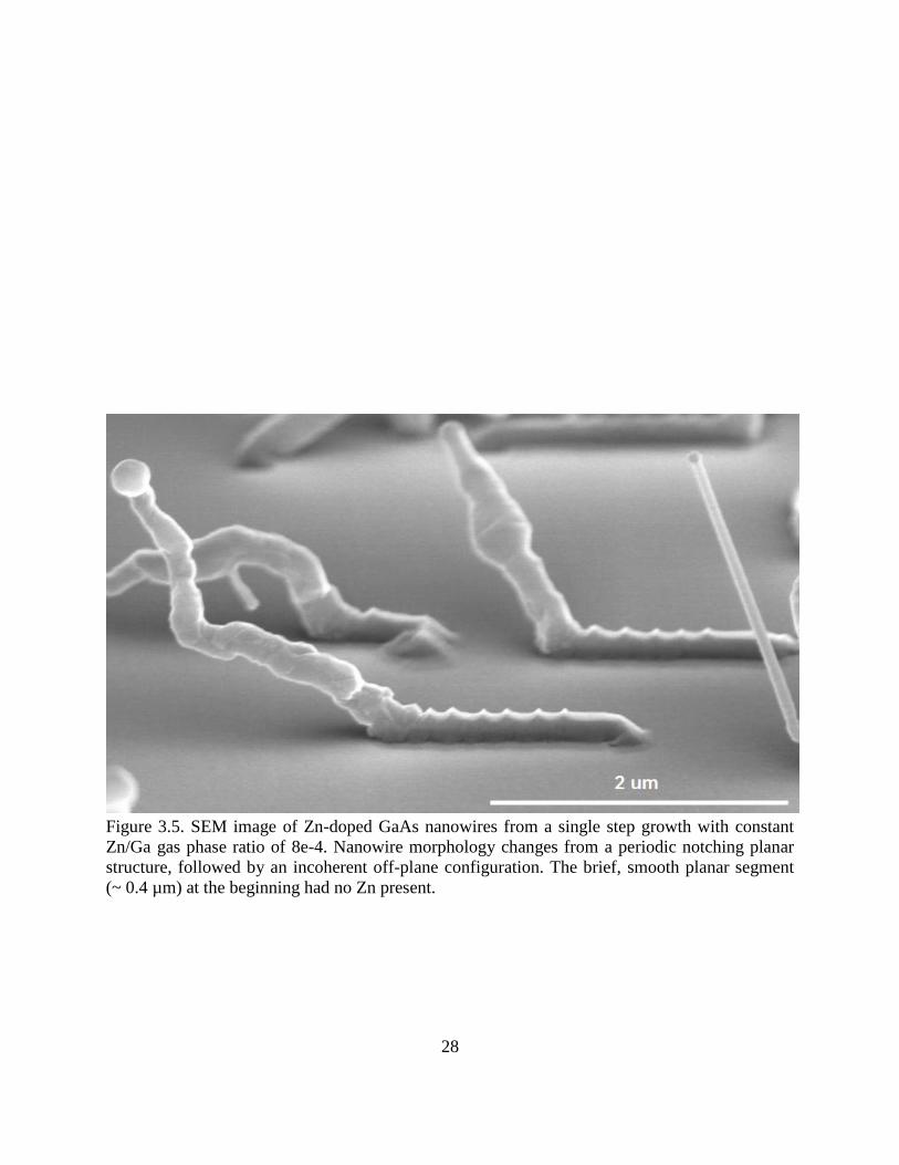
To examine the Zn doping profile along the planar GaAs nanowires growth direction, we
resort to one-step growth where Zn precursor is turned on at the same time as the Ga precursor
and remains at the same ratio throughout the nanowire growth. Shown in Figure 3.5 is the
evolution of growth orientation and topography as Zn-doped GaAs nanowire growth proceeds
for a gas phase DEZn/TMGa doping ratio of 0.08%. Interestingly, wires grown at this ratio that
appear to be planar initially (as in Figure 3.1b) become non-planar after some critical distance,
yet this did not occur with the 0.008% nanowires. This implies that zinc incorporation in
nanowires increases over time until it reaches a critical point where it perturbs normal nanowire
growth. Our observation is consistent with a previous report [4] on <111> vertical nanowires in
which Zn doping increases gradually along the growth direction under constant Zn precursor
flow. This may be attributed to the longer saturation time for Zn in Au compared to Ga in Au,
leading to a delayed or accumulation effect of Zn impurity, which has been observed by Gutsche
et al. [4] in their studies of p-type doping in vertical GaAs nanowires. This is an important
property to take note of when considering what doping concentrations are appropriate for device
dimensionality such as the channel length of a FET, as well as the possibility of creating a
natural doping concentration gradient within the wire without extrinsically changing the flow
rate for the creation of modulation doped nanowires.
18
It is remarkable that Zn incorporation at levels as low as 0.008% in planar GaAs
nanowires is sufficient to alter the atomic structure (twin plane formation) and crystal
orientation. This phenomenon presumably originates from the nucleation process in the VLS
mechanism, where any perturbation at the atomic level, such as dopant incorporation, can be
critical to the free energy of the interface between metal catalyst and solid surface, and the edges.
3.2 Suspended Film
To further explore the parameters that influence the VLS nanowire growth mechanism,
we investigated growth on suspended thin film membranes. Membranes have been reported to
have properties that are different for growth than normal bulk substrates. The main property that
makes them so attractive is their ability to be more compliant [9] with nanostructures that cause
stress because there is no restoring force on the backside of the suspended film. This allows
suspended film to accommodate structures that were not realizable on bulk substrates. Another
benefit of suspended films is the possibility of allowing epitaxial growth to occur on both sides
of the film, enabling the prospect of double-density nanostructures.
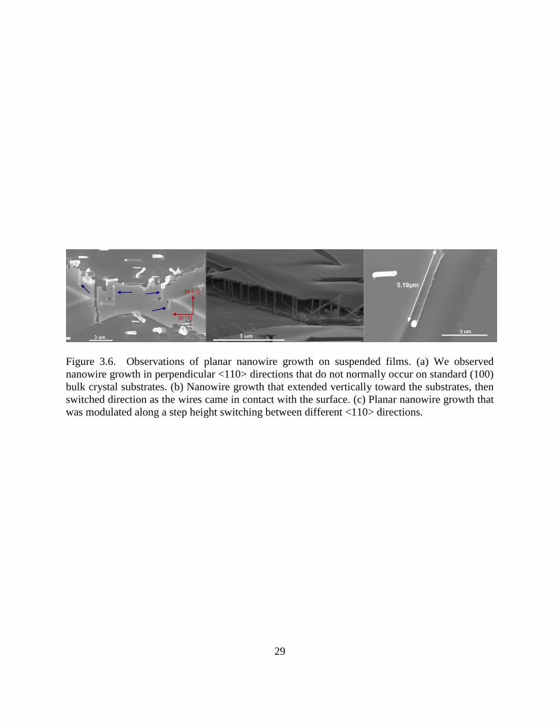
Figure 3.6 shows the results that were observed in the SEM. First we observe a shift in
growth direction not normally seen on bulk substrates. Normally planar nanowires grow in the
[0-11] and [01-1] directions, but on suspended films wires have been observed growing in the
[011] and [0-1-1] directions. This is indicative of how important the substrate conditions are for
nanowire growth. Further modulation of nanowire growth directions may be possible by thinning
the suspended film even more or changing other properties of the film. Next we noticed large
holes were created in the suspended film, usually with a nanowire growing at the end of the hole
that developed. We concluded that this was due to the Au particle alloying with the GaAs
19
suspended film during the anneal phase. It is interesting to note how much of the substrate the
Au particle actually consumes during annealing and how mobile the gold is on such thin films.
Another phenomenon of interest is that some nanowires actually grew off the edge of a
suspended direction, grew normal to the substrate then collided with the surface and then grew in
non-planar directions. This has been observed in Si nanowires with the use of oxide [10] as a
sacrificial layer, but without a change in growth direction. These results hint at the future of
creating 3D nanostructures by intentionally altering nanowire growth directions to fabricate
elaborate nanowire arrays. Lastly, we have witnessed the guiding of nanowire growth by
guiding it along a high step barrier. Figure 3.6c shows the nanowire periodically changing
growth direction within the family of <110> direction as it grows along a barrier that is angled
along a <100> direction. The barrier forms as a result of the undercutting of the GaAs suspended
film; the nanowire is following along the Al.75GaAs layer. The zigzag-like pattern is highly
periodic and new physics could be unearthed in such an alternating pattern. Modulation of the
nanowire growth direction increases the likelihood of nanowires being a fundamental building
block for future nanotechnology devices.
3.3 Indium Perturbation
Indium is an important element in the synthesis of compound semiconductors for its
capability of not only lowering the bandgap energy in ternary and quaternary materials but also
functionalizing films by inducing strain from its larger atomic size. Incorporating indium into the
core of GaAs wires will be essential in improving the variety of heterostructures that can be
fabricated such as lasers, transistors [11] and diodes from nanowires. However, since indium
notably changes the lattice structure, the possibility of indium incorporation perturbing growth
20
direction in planar nanowires was investigated in this report. TMI was turned on halfway into
growth to see whether the presence of indium would alter the growth direction of the already
planar nanowires and compare to the results of the Zn doping experiments. In/Ga molar ratios
from 8.0 x 10⁻⁵
to 2 x 10⁻²
were investigated as well as two independent growths not included in
the DOE with molar ratios that would be equivalent to an In.50GaAs and InAs film. Visual
inspection shows that growth direction and crystallographic integrity remain intact although
some nanowires exhibit a sharp notch approximately when TMI is turned on; however, this is not
systematic across all wires and could be attributed to the 15 s pause time when no metalorganics
are flown. This result is unexpected, especially since other groups have done work on fabricating
InGaAs wires and observed changes with increasing TMI flow rates [12]. Interestingly enough,
the growths with the higher indium contents produce reduced wire growth (dominantly in the
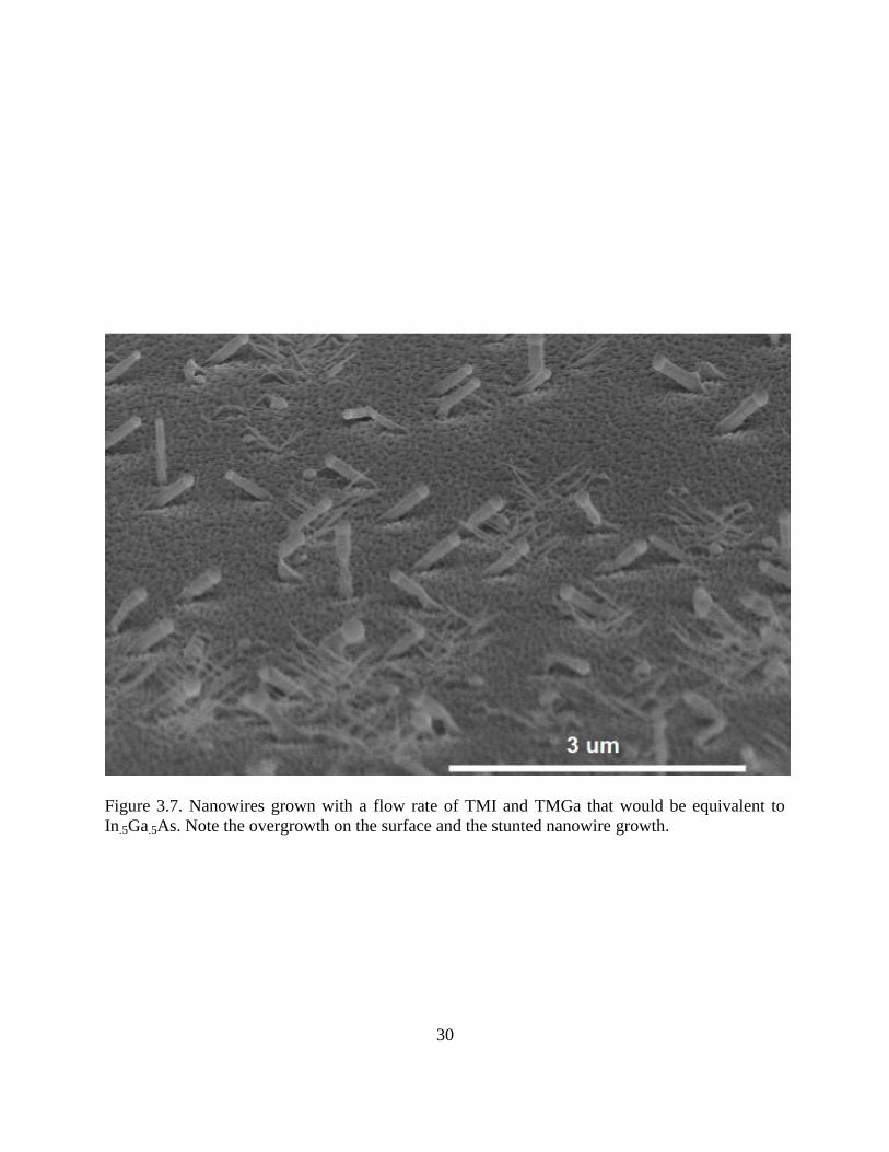
<111> direction) and drastically increased epi-growth on the surface. Figure 3.7 shows that there
is significant growth on the surface. This epi-growth resembles a metamorphic film that is
discontinuous along the surface with large porous holes throughout. There are also no visible
planar wires on the surface. Whether the change is caused by the surface impinging on planar
growth, strain inducing overgrowth on the surface, or presence of indium in the core of the
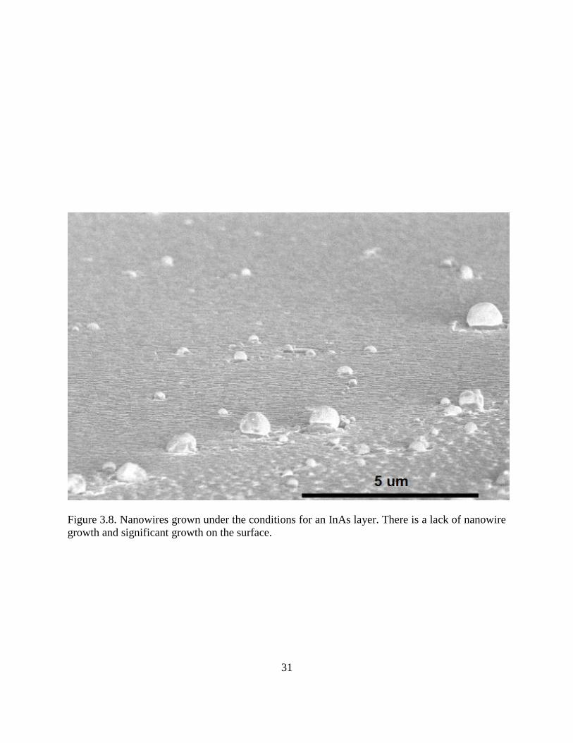
nanowire remains unknown without further analysis. Figure 3.8 shows that when nanowires are
grown with conditions suitable to grow an InAs layer, virtually no nanowires are formed, and
inspection reveals considerable growth on the surface. Furthermore, large trapezoidal shaped
InAs mesas form on the surface that resemble the shape of gold bars.
The combination of DOE and the two independent growths leads us to two possible
conclusions. First, inside the gold colloid there could be competition between In and Ga to form
an alloy with Au. With the catalyst becoming supersaturated with gallium from the substrate
21
during the 10 min anneal step, perhaps the Au-Ga alloy inhibits indium inclusion and limits the
amount of indium that will be incorporated into the wire and therefore leads to excess
overgrowth on the surface of the substrate. Another possibility could be that indium prefers
growth on the surface of the GaAs substrate over alloying with the gold catalyst. Dick et al.’s
experiments with InAs nanowires [13] may shed some light on what is occurring with the
synthesis of InGaAs wires. It has been shown that with Au-seeded InAs wire growth, when the
In-Au reach a growth temperature above their eutectic point, nanowire growth ceases. It is
possible that the ternary alloy of InGaAs has a liquid phase temperature at or below the growth
temperature of 460 °C which could prevent InAs precipitation from the Au colloid. More
experimentation and analysis, such as HR-TEM, EDS and other spectroscopy, needs to be
completed before the Au-InGaAs system will be fully understood. Further analysis will be
completed in the future.
3.4 Off-Cut Samples
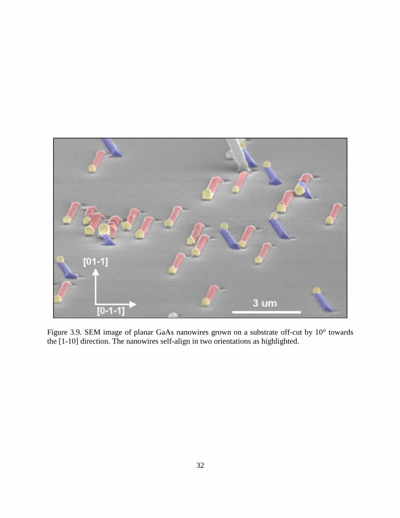
Altering the surface of the substrate can have notable effects on nanowire growth. This is
especially important for planar nanowires as they interact with the substrate along the entire
length of the wire, in contrast to vertical wires which only interact at their base. To illustrate this,
we grew nanowires on substrates that were off-cut 10° towards the [1-10] direction; the results
are outlined in Figure 3.9. Normally, planar wires grow parallel in either the [01-1] and [0-11]
directions. Once grown on the off-cut sample, they exhibit angled growth trajectories that differ
from their normal paths and are no longer parallel. The normally [01-1] wires grow ~10.19° off-
angled while the [0-11] wires are ~8.16° off-angled, and both are rotated away from the off-cut
direction. Planar nanowires have been observed intersecting, as in Figure 3.9, which does not
22
occur normally on (100) substrates; this could lead to interesting device possibilities. The
nanowires also appear to be rotated on their own axis, which reveals new crystal facets along
their growth direction. The fact that the wires rotate towards the same direction, combined with
the results of other studies [14] on substrate orientation concerning nanowire growth, leads to the
possibility that there could be an orientation where the nanowires all align in the same direction
or even cross each other perpendicularly, which could potentially be utilized in future devices.
This is extremely important as aligning nanowires is non-trivial and is currently an active area of
nanowire research.
3.5 References
[1] A. Maaßdorf and M. Weyers, "In-situ etching of GaAs/AlxGa1-xAs by CBr4," Journal of
Crystal Growth, vol. 310, pp. 4754-4756, July 2008.
[2] K. Nguyen Hong, L. Pavesi, D. Araujo, J. D. Ganiere, and F. K. Reinhart, "A model for
the Zn diffusion in GaAs by a photoluminescence study," Journal of Applied Physics,
vol. 69, pp. 7585-7593, June 1991.
[3] D. Stichtenoth, K. Wegener, C. Gutsche, I. Regolin, F. J. Tegude, W. Prost, M. Seibt, and
C. Ronning, "P-type doping of GaAs nanowires," Applied Physics Letters, vol. 92, pp.
163107-3, Apr. 2008.
[4] C. Gutsche, I. Regolin, K. Blekker, A. Lysov, W. Prost, and F. J. Tegude, "Controllable
p-type doping of GaAs nanowires during vapor-liquid-solid growth," Journal of Applied
Physics, vol. 105, pp. 024305-5, Jan. 2009.
[5] R. E. Algra, M. A. Verheijen, M. T. Borgstrom, L.-F. Feiner, G. Immink, W. J. P. van
Enckevort, E. Vlieg, and E. P. A. M. Bakkers, "Twinning superlattices in indium
phosphide nanowires," Nature, vol. 456, pp. 369-372, Nov. 2008.
[6] S. A. Fortuna, J. Wen, I. S. Chun, and X. Li, "Planar GaAs nanowires on GaAs (100)
substrates: Self-Aligned, nearly twin-defect free, and transfer-printable," Nano Letters,
vol. 8, pp. 4421-4427, Nov. 2008.
23
[7] P. Caroff, K. A. Dick, J. Johansson, M. E. Messing, K. Deppert, and L. Samuelson,
"Controlled polytypic and twin-plane superlattices in III-V nanowires," Nature
Nanotechnology, vol. 4, pp. 50-55, Nov. 2009.
[8] Q. Xiong, J. Wang, and P. C. Eklund, "Coherent twinning phenomena: Towards twinning
superlattices in III-V semiconducting nanowires," Nano Letters, vol. 6, pp. 2736-2742,
Nov. 2006.
[9] M. Huang, C. S. Ritz, B. Novakovic, D. Yu, Y. Zhang, F. Flack, D. E. Savage, P. G.
Evans, I. Knezevic, F. Liu, and M. G. Lagally, "Mechano-electronic superlattices in
silicon nanoribbons," ACS Nano, vol. 3, pp. 721-727, Feb. 2009.
[10] J. Q. Nathaniel, W. Wei, and I. K. Theodore, "Guiding vapor-liquid-solid nanowire
growth using SiO2," Nanotechnology, p. 145303, Mar. 2009.
[11] S. A. Fortuna and X. Li, "GaAs MESFET with a high-mobility self-assembled planar
nanowire channel," Electron Device Letters, IEEE, vol. 30, pp. 593-595, Jun. 2009.
[12] Y. Kim, H. J. Joyce, Q. Gao, H. H. Tan, C. Jagadish, M. Paladugu, J. Zou, and A. A.
Suvorova, "Influence of nanowire density on the shape and optical properties of ternary
InGaAs nanowires," Nano Letters, vol. 6, pp. 599-604, Feb. 2006.
[13] K. A. Dick, K. Deppert, T. Martensson, B. Mandl, L. Samuelson, and W. Seifert, "Failure
of the vapor-liquid-solid mechanism in Au-assisted MOVPE growth of InAs nanowires,"
Nano Letters, vol. 5, pp. 761-764, Mar. 2005.
[14] M. Mattila, T. Hakkarainen, H. Jiang, E. I. Kauppinen, and H. Lipsanen, "Effect of
substrate orientation on the catalyst-free growth of InP nanowires," Nanotechnology, vol.
18, pp. 155301-155301, Mar. 2007.
24
3.6 Figures
Figure 3.1. SEM images from a two-step growth where Zn source is turned on halfway into the
nanowire growth, with a gas phase Zn/Ga molar ratio of (a) 1.6e-2 zoomed out, (b) 1.6e-2 view
of a single nanowire, (c) 8e-5 zoomed out, (d) 8e-5 view of a single nanowire.
25
Figure 3.2. Plot of the notch period in Zn-doped planar nanowires as a function of Au catalyst
particle size, from two doping levels (Zn/Ga ratio) as indicated. The solid line is the best linear
fit to the data with a slope of 0.91, indicating a strong correlation between the notch period and
the catalyst particle size.
26
Figure 3.3. SEM image showing solid precipitants (presumably Zn; see text) on the surface of
the Au seed particle in a moderately Zn-doped planar nanowire. The particulate is more
prevelant with increasing Zn/Ga gas phase ratios.
27
Figure 3.4. Left: A bright-field TEM image showing twin boundaries in the nanowire. (The
growth direction of the nanowire is along [110], while the twin boundary is in the (111) plane.)
Right: Selected-area electron diffraction pattern along the [110] zone axis of the nanowire
showing the existence of twin boundary.
28
Figure 3.5. SEM image of Zn-doped GaAs nanowires from a single step growth with constant
Zn/Ga gas phase ratio of 8e-4. Nanowire morphology changes from a periodic notching planar
structure, followed by an incoherent off-plane configuration. The brief, smooth planar segment
(~ 0.4 µm) at the beginning had no Zn present.
29
Figure 3.6. Observations of planar nanowire growth on suspended films. (a) We observed
nanowire growth in perpendicular <110> directions that do not normally occur on standard (100)
bulk crystal substrates. (b) Nanowire growth that extended vertically toward the substrates, then
switched direction as the wires came in contact with the surface. (c) Planar nanowire growth that
was modulated along a step height switching between different <110> directions.
30
Figure 3.7. Nanowires grown with a flow rate of TMI and TMGa that would be equivalent to
In.5Ga.5As. Note the overgrowth on the surface and the stunted nanowire growth.
31
Figure 3.8. Nanowires grown under the conditions for an InAs layer. There is a lack of nanowire
growth and significant growth on the surface.
32
Figure 3.9. SEM image of planar GaAs nanowires grown on a substrate off-cut by 10° towards
the [1-10] direction. The nanowires self-align in two orientations as highlighted.
33
4. QUANTUM DOTS
4.1 Quantum Dots
Semiconductor devices are constantly being scaled down further and further. Aside from
increased device density, there is another benefit as new characteristics reveal themselves with
reduced dimensions. As devices scale down, so do their available energy states. When the size of
the device approaches the De Broglie wavelength of an electron, the density of available energy
states sharpens and ceases to behave like a quasi-continuum as in the case of bulk 3D crystals. If
the device is confined in one dimension, a quantum well, density of states behaves like a step
function with constant number of available states per subband. Further confined in another
dimension, a quantum wire, the available states follow E-1/2
where E is the energy of the carrier.
Finally, when the device is confined in all three dimensions, a quantum dot, the density of states
becomes a set of discrete states resembling a delta-function at specific energies. The sharpening
of the energy states implies that it is possible to produce devices that operate at different
wavelengths simply by varying the size of the quantum dots. This has important ramifications for
optical devices such as photon detectors, lasers, LEDs and other optoelectronics. By varying the
materials, the substrate, and the growth conditions, a variety of novel nanostructures can be
produced for both fundamental studies of quantum confined systems, and for advanced photonic
devices.
Although quantum dots are a heavily researched field and hold much promise to become
an industry staple, they do have some shortcomings. Since quantum dots generally have a small
volume, their emission and absorption tend to be weaker, so they have to be fabricated in high
densities but without aggregating into large clusters which no longer have the energy
34
quantization properties. In order to create discrete quantum dots but in high enough densities to
be useful, a method called strain-induced self-assembly is utilized [1]. This method depends not
on lithographic techniques, which tend to be problematic and expensive at such small
dimensions, but rather on heteroepitaxy. The detailed growth method of the quantum dots is
explained further in the experimental section of this thesis.
III-V heteroepitaxy has been the traditional route for self-assembled III-V quantum dots
(II-VI quantum dots are mostly formed by solution based colloidal synthesis) [2]. The direct
bandgap, tunable lattice mismatch, and wider selection of materials make it a robust system for
this type of growth. There are issues that make it less attractive for broad commercialization: III-
V materials, when compared to silicon, have much higher material cost, and long-term
investment may be an issue due to the rarity and uncertain future availability of indium and
gallium in the Earth’s crust [3, 4]. Most of the cost is in the substrate, which provides necessary
functionality to the quantum dot systems. For example, for self-assembled InAs QDs on a GaAs
substrate, the dots themselves are the active device while the substrate provides a quantum
confinement barrier and the strain necessary for the self-assembly to occur. The function that the
GaAs provides could potentially be provided by other substrates, but the caveat is that the
substrate has to provide the correct amount of strain. With too little strain, the dots coalesce into
a continuous layer, while with too much strain, the dots are incoherent with crystal defects.
These defects can act as traps for carriers and degrade the quantum efficiency of the device.
Recently, suspended membranes have been investigated as a potential solution to some of
the economic issues with self-assembled quantum dots. Fabrication of suspended thin silicon
membranes is outlined in the experimental section of this thesis. Researchers have discovered
unique phenomenon when strain-mismatched Ge quantum dots were grown on thin Si
35
membranes [5]. Remarkably, the strain interaction with the thin membrane naturally orders the
dots in a continuously alternating fashion with one dot on the top and one on the bottom of the
membrane, as shown in Figure 4.1. As a secondary effect, this causes the film to undulate, with
QDs atop the crest and at the bottom of the trough. The interaction between the dot and the
membrane shows that the thin membrane is very compliant and will adjust readily to
accommodate the strain of the quantum dot since there is no restoring force on the thin
membrane as with a bulk substrate. The degree of compliance is supposed to be larger than for
solid films, which should lead to the possibility of producing quantum dot materials on
membranes that would normally cause dislocations or metamorphic growth on bulk substrates.
III-V materials were chosen as the perfect candidate to test this hypothesis as the lattice
mismatch between GaAs and Si is similar to Ge and Si, and InAs on Si provides a much larger
mismatch than elemental Ge on Si. It will also be of interest to verify that the dots could possibly
align themselves for material systems in general, as in the case of Ge QDs on Si membranes.
GaAs quantum dots were grown on silicon membranes at various growth conditions to gauge the
effect of different growth parameters on the quality of the quantum dot produced. Coverage,
growth interruption, and temperature were chosen as the parameters to vary independently.
4.2 Effect of Coverage
Coverage, referring to the number of intended monolayers grown by adjusting precursor
flow rates and growth time, is an important parameter to consider when growing quantum dots.
The amount of coverage dictates the growth mode. At low coverage, growth either forms 2D
islands, similar to Frank-van der Merwe growth modes, that do not have enough material to
aggregate into quantum dots, or forms some dots that are at too low of a density to be useful. At
36
high coverage, dots will become incoherent in order to reduce the intrinsic strain by creating
dislocations instead of forming a psuedomorphic interface. At very high levels of coverage, the
dislocated dots form in extremely high densities and can amalgamate into thin metamorphic
films. The type of materials system determines which coverage range produces highest quality
quantum dots.
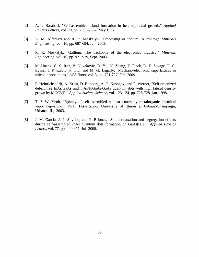
Figure 4.2 shows the effect of coverage on the size and density of GaAs QD growth
suspended silicon membranes at a growth temperature of 450 oC, with a constant flow of 5 sccm
of TMGa at growth times of 2 s, 4 s and 20 s. There is a direct relationship between density, size
and the appearance of QDs that are abnormally large compared to other QDs. These large QDs
are possibly formed from increased Oswalt's ripening due to the larger amount of precursor
present at higher coverage. However, no difference between the growth on suspended
membranes and supported silicon films has been observed at all coverages under the specified
growth temperature.
4.3 Effect of Growth Interruption
Growth interruption is essential in the growth of QDs in order to create coherent and
dislocation-free quantum dots. This is achieved by interrupting the flow of precursors while
keeping the H2 carrier gas and maintaining constant growth temperature. The interruption allows
time for material to diffuse, coalesce and form proper Stranski-Krastanov quantum dots. In
arsenic based crystals that use arsine as their hydride for an As precursor, this is especially
crucial. Heinrichsdorff et al. have done research on the effect of AsH3 post-dot formation before
the chamber is cooled down [6]. They found that the hydrogen radicals from the arsine molecule
would cause defects in their InAs quantum dots. The best solution they found is to actually turn
37
off arsine flow during their growth interruption, which resulted in higher quality dots. Excess
arsine in the growth chamber, which is not necessary for growth and the prevention of out-
diffusion of As from the substrate, is limited to prevent hydrogen incorporation, making low
V/III ratio a priority. The effect of GI time on the QD quality is hard to quantify using
microscopy and is usually done with spectroscopy methods [7]. Spectroscopy measurements will
be carried out in the future for this project. GI time was varied from 30 to 90 s and no apparent
physical differences have been observed between dots grown on the suspended membrane and
those on supported silicon film.
4.4 Effect of Temperature
Temperature controls multiple aspects of QD growth, and is one of the most important
parameters to consider when growing QDs on suspended films. Temperature affects the crystal
growth in general as well as QD formation. In MOCVD, different precursors pyrolyse, or crack,
under different temperatures, which causes their pyrolysis efficiency to change with temperature.
Hence it is possible to get increasing coverage from the same flow rate of precursor simply by
increasing the temperature. Secondly, some materials tend to be more diffusive at higher
temperatures than others. This is important when using indium in quantum dot growth. Indium
has a tendency to be extremely mobile and segregate at higher temperatures [8]. Material also
tends to diffuse farther at higher temperatures, leading to naturally larger quantum dots. For
GaAs QD growth on silicon membranes, an interesting phenomenon has been observed when the
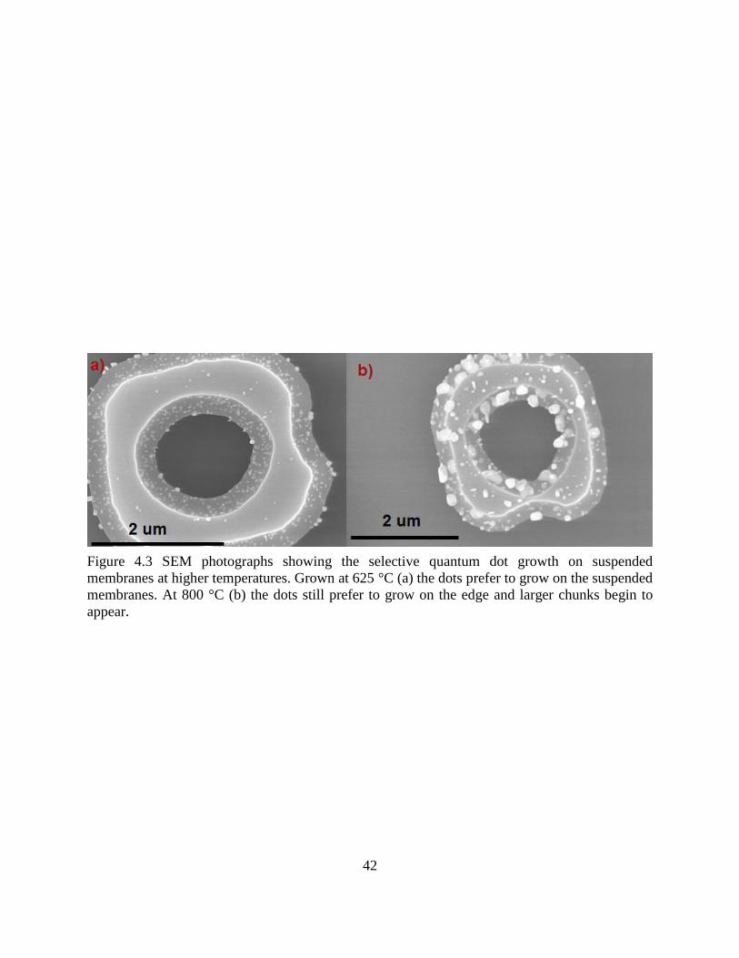
growth temperature is varied. Figure 4.3 shows the SEM images of GaAs QDs grown at 625 °C
and 800 °C on a ring-shaped silicon substrate with suspended membranes at the edges and the
supported part in the middle. It can be seen that QDs selectively grow on the suspended
38
membrane (appear to be on the backside), with hardly any growth on the supported silicon
substrate. With further increased temperatures, QD growth maintains its preference of the
membrane while combining into large chunks, probably due to higher diffusivity and increased
Oswalt's ripening. In contrast, the QDs shown in Figure 4.2 were grown at 450 °C and no
selectivity was exhibited between suspended and supported substrates.
The selectivity observed is most likely a result of increased mobility/diffusivity of
precursor materials at higher temperature. The tendency of QDs to grow on the backside of the
membrane could possibly be due to the larger number of nucleation points underneath of the
suspended edge, as it was the Si/SiO2 interface before released. The exact mechanism is not
entirely known at this time and is under investigation. The preferential growth location leads to
the possibility of making selective area growth using suspended regions to pattern QDs
indirectly.
In summary, no ordering has been observed under all the conditions explored so far for
the growth of GaAs quantum dots on silicon membranes. The only difference from bulk silicon
substrates appears at high growth temperature, where preferential growth on the suspended part
occurs. Further exploration of III-V quantum dots on suspended silicon membranes will include
the growth on thinner (< 13 nm) membranes, continued optimization of growth conditions, and
InGaAs QD growth. Ordered III-V quantum dots on silicon could be candidates for room
temperature thermoelectric Si-based nanosystems with discrete minibands [5].
4.5 References
[1] J. M. Moison, F. Houzay, F. Barthe, L. Leprince, E. Andre, and O. Vatel, "Self-organized
growth of regular nanometer-scale InAs dots on GaAs," Applied Physics Letters, vol. 64,
pp. 196-198, Jan. 1994.
39
[2] A.-L. Barabasi, "Self-assembled island formation in heteroepitaxial growth," Applied
Physics Letters, vol. 70, pp. 2565-2567, May 1997.
[3] A. M. Alfantazi and R. R. Moskalyk, "Processing of indium: A review," Minerals
Engineering, vol. 16, pp. 687-694, Jun. 2003.
[4] R. R. Moskalyk, "Gallium: The backbone of the electronics industry," Minerals
Engineering, vol. 16, pp. 921-929, Sept. 2003.
[5] M. Huang, C. S. Ritz, B. Novakovic, D. Yu, Y. Zhang, F. Flack, D. E. Savage, P. G.
Evans, I. Knezevic, F. Liu, and M. G. Lagally, "Mechano-electronic superlattices in
silicon nanoribbons," ACS Nano, vol. 3, pp. 721-727, Feb. 2009.
[6] F. Heinrichsdorff, A. Krost, D. Bimberg, A. O. Kosogov, and P. Werner, "Self organized
defect free InAs/GaAs and InAs/InGaAs/GaAs quantum dots with high lateral density
grown by MOCVD," Applied Surface Science, vol. 123-124, pp. 725-728, Jan. 1998.
[7] T. S.-W. Yeoh, "Epitaxy of self-assembled nanostructures by metalorganic chemical
vapor deposition," Ph.D. Dissertation, University of Illinois at Urbana-Champaign,
Urbana, IL, 2003.
[8] J. M. Garcia, J. P. Silveira, and F. Briones, "Strain relaxation and segregation effects
during self-assembled InAs quantum dots formation on GaAs(001)," Applied Physics
Letters, vol. 77, pp. 409-411, Jul. 2000.
40
4.6 Figures
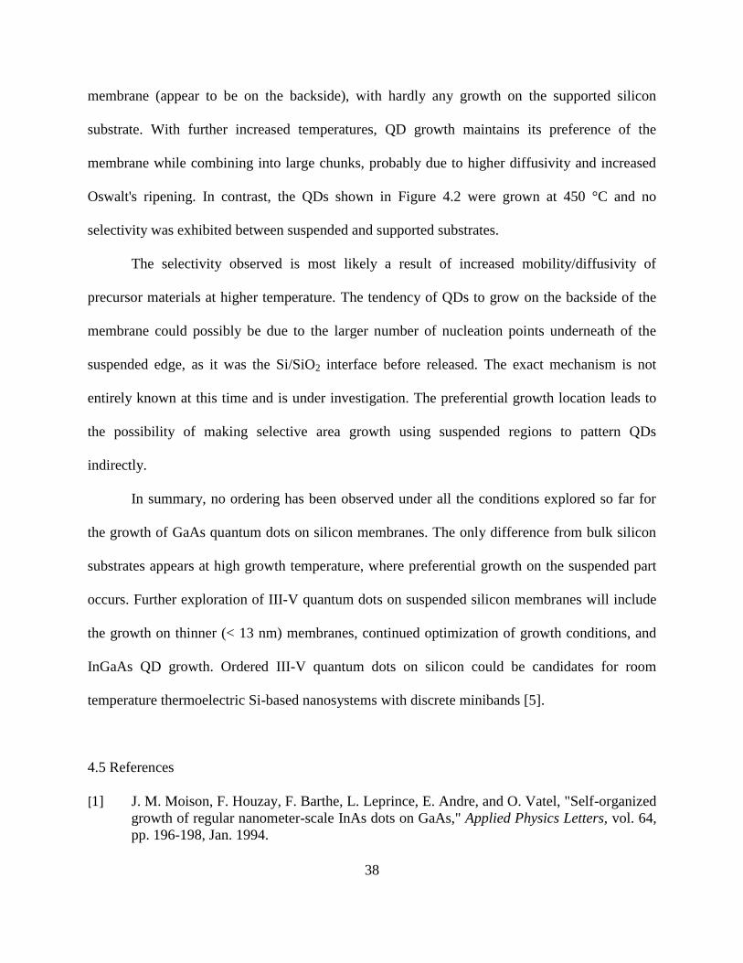
Figure 4.1 Quantum dots on the top and bottom of a suspended silicon membrane. The spacing
between the dots is ~ 350 nm [4].
41
Figure 4.2 SEM photos showing the effect of coverage on GaAs quantum dots grown on
suspended silicon membranes. At 1.65 ML the dots are barely visible under SEM (a), while at
3.3 ML (b) the dots are more pronounced and clearly visible. At high coverages, 16.5 ML (c),
the dots start to become larger and denser, beginning to merge with one another.
42
Figure 4.3 SEM photographs showing the selective quantum dot growth on suspended
membranes at higher temperatures. Grown at 625 °C (a) the dots prefer to grow on the suspended
membranes. At 800 °C (b) the dots still prefer to grow on the edge and larger chunks begin to
appear.
43
5. CONCLUSION
5.1 Summary
The phenomena associated with incorporating Zn, growing on suspended membranes
and 10° off-cut substrates with VLS planar <110> GaAs nanowires have been investigated.
Nanowires that have been grown with DEZn present have produced alternating twin plans in
the <111> crystal direction that have controllable period lengths roughly correlated to the size
of the catalyst particle. Planar nanowires grown on suspended membranes reveal new growth
directions that are not apparent on bulk substrates. Planar GaAS nanowires usually grow in the
[0-11] and [01-1] crystal directions but appear to grow in [011] and [0-1-1] only on GaAs
suspended membranes, which could be used for alignment and for planar nanowire arrays.
Planar nanowires grown on 10° off-cut samples exhibit asymmetrical rotation away from the
off-cut direction. The asymmetrical rotation shows the possibility of creating wires that could
face all one direction or cross at specified angles, which could be useful in creating devices
that would require such specifications.
III-V self-assembled quantum dots on suspended thin silicon membranes are being
investigated as a possible solution to the integration of compound and elemental
semiconductor materials. Controlling aspects of growth using coverage, growth interruption
and temperature, as well as their effects, have been studied. Coverage has been shown to
influence quantum dot size and density, while growth interruption effects, while having no
external features, should prove useful in the creation of high quality dots once the optical
analysis phase of the study begins. Temperature has shown the largest effect by not only
controlling QD size and density, but also exhibiting influence over selective area growth,
44
leading to the possibility of patterning QDs where lithographic techniques can not be used
effectively.
5.2 Future Directions
In addition to the interesting crystal phenomenon associated with Zn-doped planar
<110> GaAs nanowires, there is a bevy of potential electronic and optical applications suited
for such a structure. Theoretically there has been speculation about the possibility of
minibands [1] and carrier tunneling naturally occurring due to the highly periodic structure of
the nanowire twin formation [2]. Preliminary on-substrate electrical measurements have been
performed with the Zn-doped nanowires. The tests revealed an abnormally leaky substrate that
made it impossible to probe individual nanowires. Control experiments done on undoped
nanowires showed very low electrical leakage, pointing to the dopant as the culprit. Future
experiments will be done to try to encourage Zn incorporation only into the nanowire itself,
and to limit diffusion into the substrate. If this is not attainable, methods to circumvent the
substrate, such as removing the nanowire from its host or suspending it over air to create
insulation, will be investigated.
The inclusion of indium in GaAs nanowires will be very beneficial in the future of
planar wires to widen the possibility of potential devices. Preliminary results show there is
little indication of indium incorporation in initial experiments. More trials need to be
completed, although V/III ratio [3] and growth temperature may play important roles in how
indium is incorporated in the wire, especially when considering the results of a study on
vertical InAs wire growth [4]. Wires grown on suspended films exhibit how accommodating
planar nanowires are to their substrate as well as how much of a role substrate plays in their
45
growth. Different types of substrate growth conditions are being looked into, such as the role
of thickness in suspended membrane nanowire growth and how various types of obstacles
affect growth such as barriers, pits, gradual slopes and abrupt changes in crystal planes. Lastly,
research on planar nanowire growth on off-cut substrates is being furthered. Substrates of
various degrees of off-cuts and different orientations are being examined to learn whether one
can grow nanowires in a desired direction, or at the least eliminate the dual growth direction
and have only one direction available to improve their alignment in future devices.
The next steps in the study of self-assembled QDs on suspended silicon membranes
will be to complete the study of all the growth parameters on QD formation. Parameters such
as deposition rate, material composition and membrane thickness will be adjusted to observe
any ordering besides the already observed selective area growth. Once all the parameters are
observed, those that prove to create the highest quality dots will then be tested with more
thorough metrology, such as TEM and spectroscopy, in order to gauge their quality. TEM will
be useful to observe any crystalline defects, while spectroscopy tests will prove beneficial to
determine their optical characteristics.
5.3 References
[1] R. E. Algra, M. A. Verheijen, M. T. Borgstrom, L.-F. Feiner, G. Immink, W. J. P. van
Enckevort, E. Vlieg, and E. P. A. M. Bakkers, "Twinning superlattices in indium
phosphide nanowires," Nature, vol. 456, pp. 369-372, Nov. 2008.
[2] P. Caroff, K. A. Dick, J. Johansson, M. E. Messing, K. Deppert, and L. Samuelson,
"Controlled polytypic and twin-plane superlattices in III-V nanowires," Nature
Nanotechnology, vol. 4, pp. 50-55, Nov. 2009.
[3] S. A. Dayeh, E. T. Yu, and D. Wang, "III-V nanowire growth mechanism: V/III ratio and
temperature effects," Nano Letters, vol. 7, pp. 2486–2490, Jul. 2007.
46
[4] K. A. Dick, K. Deppert, T. Martensson, B. Mandl, L. Samuelson, and W. Seifert, "Failure
of the vapor-liquid-solid mechanism in Au-assisted MOVPE growth of InAs nanowires,"
Nano Letters, vol. 5, pp. 761-764, Mar. 2005.