Embed Size (px)
Citation preview

Guidelines
Rework of Electronic Assemblies
Qualifiable Processes for Rework
German Electrical and Electronic Manufacturers’ Association

Rework of Electronic Assemblies
Published by:ZVEI - Zentralverband Elektrotechnikund Elektronikindustrie e. V. German Electrical and Electronic Manufacturers’ Association PCB and Electronic Systems DivisionLyoner Strasse 960528 Frankfurt am Main, Germany
Editor: Dr Christoph Weiß, ZVEIPhone: +49 69 6302-437E-mail: [email protected] www.zvei.org/pcb-es
Authors:Thomas Lauer, Airbus DS Electronics and Border Security Peter Fischer, Batiloy Company for Soldering Technology Sebastian Bechmann, Christian Koenen Harald Grumm, Ersa Jörg Nolte, Ersa Helge Schimanski, Fraunhofer Institute for Silicon TechnologyFranz Leitenstern, Martin Franz-Josef Schoeferle, Rohde & Schwarz Messgerätebau Conrad Wagenbrett, Wagenbrett Dr. Lothar Weitzel, Würth Elektronik Dr. Helmut Schweigart, Zestron Europe Janos Tolnay, Zevac Stefan Penzenstadler, Zollner Electronics Michael Zimmerer, Zollner Electronics Florian Gruber, Zollner Electronics
November 2017
This document may be reproduced free of charge in any format or medium, includ-ing in part, provided it is used correctly and not in a misleading context. The ZVEI copyright must be visible and the title of the document must be specified. A free copy of the document in which ZVEI material is used must be made available. The ZVEI assumes no liability for the content.
Content
1 Introduction
2 General Aspects
2.1 Definitionofreworkandrepair
2.2 The line process as a reference
2.3 Norms, standards and guidelines
2.4 Flux interaction "No-clean - but..."
2.5 Parameters
2.6 Acceptance requirements
2.7 Printed circuit board
2.8 Components
2.9 MSL-Moisture Sensitivity Level
2.10Thermalprofiling
2.10.1 Tools and sensor positioning
2.10.2Methodologyofprofiledetermination
2.11 The nth soldering process
2.12 Heat transfer
2.13Processflows
2.13.1 When a component "must" - "can" - "must not" be reworked
2.13.2 Sequence of component replacement
2.13.3Detailedprocessflow
2.14 Device technology
2.14.1 Hand soldering devices
2.14.2 Quasi-stationary rework systems
2.15 Devices - Systems - Concepts
2.15.1 Semi-automatic hot gas rework system
2.15.2 Automatic hot gas rework system
2.15.3 Automatic IR rework system
6
7
7
7
9
12
14
16
17
27
27
29
29
29
33
34
35
35
36
39
40
40
44
45
45
49
52

3 Manual Soldering - Trials and Findings
3.1 Proven equipment within the trial series
3.2 Two typical disciplines of the manual soldering area
3.2.1 Desoldering, resetting and manually re-soldering of passive components
3.2.2 Processing of PQFP components
3.3 Findings on manual soldering
4 Findings from the R+R Studies
4.1 Thermalprofiles(target-actual)
4.2 Printed circuit board as the dominant component
4.3 Componentspecifications,orderedaccordingtotheir complexity
4.3.1 Two-pole, passive components
4.3.2 Two-pole, passive ferrite choke with high heat demand
4.3.3 ComponentswithflatGullwingconnections
4.3.4 SMT connectors in mixed SMT-THT technology
4.3.5 Classical ball grid array designs
4.3.6 Arrayconnectors(BGApin-out)
4.3.7 BGAsocket
4.4 Possible effects at assembly level
4.5 Multiple solder stress – visual/cross-section analysis
4.5.1 Assemblies after multiple solder stress in visual inspection
4.5.2 Assemblies after multiple solder stress in cross-section analysis
4.5.3 Assessmentofthemultiplesolderstressinfluence
4.6 Reballing
4.6.1 Motivation
4.6.2 Generalcourseofthereballingprocess
4.6.3 Devices - systems - concepts
4.6.4 Balling stencils
4.6.5 Reballing / recommendation for the process sequence
56
56
56
56
57
57
60
60
63
66
66
66
67
67
67
69
69
70
70
71
74
79
81
81
81
82
91
91

92
92
94
95
97
99
99
117
117
118
119
120
123
126
126
127
127
129
131
132
133
135
4.7 Stencil and process technology
4.7.1 Rework stencils for printing on printed circuit boards
4.7.2 Rework stencils for printing on components
4.7.3 Rework stencils for dipping components
4.7.4 Process engineering
5 Neuralgic Points for Consideration
5.1 Faults - cause index
5.2 Electrochemicalmigration(ECM)
5.2.1 Preconditions for the emergence of electrochemical migration
5.2.2 Formation mechanism
5.2.3 Consequences of electrochemical migration
5.2.4 Qualificationofresiduesafterrework
5.3 Overview of test results
6 Conclusion/Outlook
6.1 Reliability
6.2 Thermal processes
6.2.1 Rework/component process preference table
6.2.2 Repair/component process
7 Closing Remarks
8 Corporate and Research Partners
9 Bibliography
10 Glossary

6
1 Introduction
Keywords such as process or machine capability, six-sigma approaches, flat-rate zero-defect strategies or lean are initially oriented primarily to the high-throughput line and mass soldering processes, leaving little acceptance for (seemingly) useless, non-value-adding processes such as rework or repairing electronic flat assemblies.
Particularly within specific sectors, any additional rework or even repair step is regarded as a neglected additional disci-pline not worthy of discussion.
If these reasons for a strictly negative atti-tude are exclusively due to the fact that these exceptional corrective steps are a sup-posedly expensive measure, this might seem an acceptable justification. Unfortunately, the fundamental quality of these supple-mentary measures is often questioned with-out having considered the procedures used in detail.
These uncertainties about the assessment and design of any necessary rework or repair steps are nurtured by the supposedly poor initial situation with regard to established process principles for safe process design.
The aim and purpose of the ZVEI Rework and Repair (R+R) Working Group (WG) is to present the understanding gained in the form of an industry recommendation with regard to the chances and risks of rework and repair processes and, if necessary, to sensitise them to specific needs.
The guide is intended to enable both cus-tomers and manufacturers to identify possi-ble process limitations and process specifics and to help them develop a more consist-ent perception, need-oriented acceptance and improved understanding of the topic of rework and repair.
This guide first presents the basic consider-ations for rework and repairing assemblies.
Only rework will be covered in the guide, as its aim and purpose is to ensure the con-formity of the finished product with draw-ings and specifications.
In the event of doubt, the user must, together with his client, weigh up for his project whether or not his process is a repair as defined in chapter 2.1.
At the same time, relevant norms, standards and guidelines for the implementation of high-quality, reproducible rework or repair will be presented.
The content of this guide is based on the prior knowledge and individual experience of all members of the WG, and on the other hand the findings of the test assemblies of ZVEI-WG R+R (especially created for this purpose).
Specific risks and neuralgic points within the entire process design are presented and recommendations for implementation are given on the basis of the respective param-eters of the procedures and processes.
Irrespective of the solder alloys to be used, the effects of lead-free rework and repair with SnAg3.0Cu0.5 solders (SAC305 sol-ders) are primarily discussed in the present case, but the findings on soldering pro-cesses with other alloys can be carried over at suitable process temperatures in the light of the thermal load capacity of the assem-blies/components.
The user of the guide will be given a sum-mary of all important factors for the safe implementation of R+R processes in the form of a decision or processability matrix.

7
Only too easily are non-original value-adding processes such as rework and repair classified as repairs and not separately con-sidered.
However, a closer look is needed to properly assess the underlying procedures and con-cepts of rework, repair or modification (as a special case) if required.
A compact definition of the respective methods is provided by the IPC-T-50J [1], in which the terms are described as below.
Rework: Rework of a non-conforming article with original or equivalent processing in a way which ensures the complete consistency of the article with the corresponding draw-ings or specifications (could also definitely include a component replacement).
Modification: Revision of the functionality of a product to meet new acceptance criteria. Changes are generally necessary to take account of design changes, which are made in draw-ings, by alteration orders, etc. Changes are to be made only with the express permission and accompanied by the detailed documen-tation in the applicable documents.
Repair: Restoring the operability of a defective article in a way which does not ensure the complete consistency of the article with the corresponding drawings or specifications.
Irrespective of which type of corrective action is chosen, some basic questions must first be clarified:• Is the corrective measure only an
unscheduled transitional measure or is there a risk of it becoming routine?
• How effective is the measure? • Are there any qualitative restrictions on
the change?• Are there restrictions on reliability?• Is it possible to apply an additional
measure at all?• Are suitable ESD protection measures
implemented to protect the components and assemblies?
• Are there any restrictions with respect to moisture-sensitive components (MSL)?
• Are cleanliness, proper handling and suf-ficient employee qualification ensured?
2 General Aspects
2.1 Definitionofreworkandrepair
2.2 The line process as a modelIn order to meet the individual thermal requirements and general conditions for the reworking of electronic assemblies, the soldering processes to be applied must first be defined and assessed.
While separate consideration is particularly necessary for manually guided soldering devices (such as manual soldering irons or hot gas grinders) (see chapter 2.14.1), ther-mal conditions can be clearly defined for so-called rework systems or quasi-stationary systems (see chapter 2.14.2).
In terms of thermal conditions, the reflow line process, including the corresponding documents, is in a certain sense the refer-ence process.
The objectives of an optimised reworking step using the rework system are:• Thermal profile stability and characteristic
in line with the (reflow) line process• Transfer of the assembly requirements of
all components to the individual require-ments of the structures which are the focus of the rework
• Rework profiles may deviate from the "classic" reflow profile (DIN EN 61760-1) [2] - see chapter 2.5 - of the assembly, but in no case breach the individual com-ponent specifications.
8
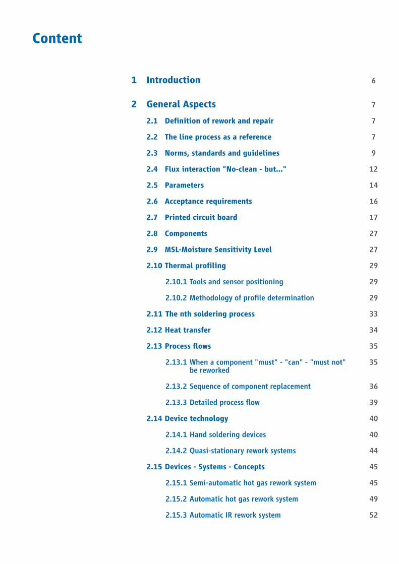
In accordance with these basic consid-erations, the local thermal profiles to be applied to individual components should be adapted as follows• Compliance with the manufacturer's
specifications (component, Printed Circuit Board (PCB) and soldering material)
• Compliance with the limits of J-STD-020 [3]
• Compliance with component handling under J-STD-033 [4]
• Compliance with the limits of J-STD-075 [5]
• Achieving the recommendations of IPC 7095 [6]
• Achieving the recommendations of IPC 7093 [7]
The following parameters (for SAC305) are recommended in addition to strict adher-ence to the minimum and maximum limits of the components for process-safe process-ing and to ensure temperature compensa-tion on the assembly (based on reflow sol-dering):• Positive temperature gradient of 0.5-2 K/s
at the solder joint (heating)1, 4
• Negative temperature gradient of 2-4 K/s at the solder joint (cooling)1, 4
• The Printed Circuit Board (PCB) temperature should not be above 190°C for more than 150 s4
• The Printed Circuit Board (PCB) tempera-ture should not be above 245 °C4
• The time above liquidus temperature (about 220 °C) at the solder joint should be between 30 s and 60 s1, 2
• The peak temperature at the solder joint should be between 230 °C and 245 °C1, 2
• The maximum temperature at the solder joint should not apply for more than 20 s
• The maximum peak package body temperature should not be more than 245 °C1
• The maximum temperature at the top of the component should not be applied for more than 20 s1, 3
The often discussed consideration of keep-ing the rework process as cool as possible seems to be plausible at first, in order to expose the components to the lowest pos-sible thermal stress. The following aspects must be considered:• Achieving stable solder joint training IMC
(Inter Metallic Compound) layer• Compliance with the minimum process
limits in order to ensure the classifica-tion of the flux residues
• Process fluctuations must be considered
For assemblies with a large thermal mass, solder profiles can be significantly longer. These should be regarded as permitted as long as the above criteria are met.
Fig. 1: Recommendation for a mild reflow profile for the rework
0 60 120 180 240 300
Source: ZVEI
250
200
150
100
50
0
Maximum PCB temperature ≤245 °C
PCB temperature above 190 °C ≤150 s
Neg. temperature gradient 2-4 K/s
Mild Rework profile
Pos. temperature gradient 0.5-2 K/s
Solder joint peak temperature230-245 °C
Time above liquidus temperature 30-60 s
Peak package body temperature ≤245 °CDuration of peak package body temperature -5 °C ≤20 s)
Time (sec)
Tem
pera
ture
(°C
)
1 Limiting values of components take priority. 2 Recommendation from the project (if the permitted process
limits are exceeded an additional crosssection analyse should
be taken to account).3 Measured maximum temperature -5 °C.4 Follow the instructions of the material manufacturer.

9
ProfileparametersMild processing
Permitted processing
Positive temperature gradient at the solder joint 1, 4
0.5-2 K/s <3 K/s
Negative temperature gradient at the solder joint 1, 4
2-4 K/s <6 K/s
Time of the Printed Circuit Board (PCB) temperature above 190 °C 4
≤150 s ≤240 s
Maximum Printed Circuit Board (PCB) temperature4
≤245 °C ≤260 °C
Time above liquidus temperature at the solder joint (about 220 °C) 1, 2
30-60 s 2 45-90 s
Peak temperature 3 Solder joint 1, 2 230-245 °C 2 235-250 °C
Duration of peak temperature 3 Soldering point
≤20 s ≤20 s
Peak package body temperature 1 ≤245 °C ≤260 °C
Duration of peak package body temperature 1, 3
≤20 s ≤30 s
1 Limiting values of components take priority. 2 Recommendation from the project (if the permitted process limits are exceeded an aaditional cross-section analyse should be taken to account 3 Measured maximum temperature -5 °C.4 Follow the instructions of the material manufacturer.
Tab. 1: Parameter-conserving and permitted processing
2.3 Norms, standards and guidelinesA large number of norms, standards and guidelines deal more or less extensively with the topic of rework, modification and repair of assemblies. Individual documents consider only partial aspects in some cases with contradictions. The reader will now be given an overview of the most important works and contents and thus a basis for taking decisions.
The guide refers to the latest revision of the documents at the time of preparation. Future revisions of the listed documents might lead to a significant change, which cannot be considered here.
Document Document name Main contents
IPC-T50 [1] Terms and Definitions for Interconnecting and Pack-aging Electronics Circuits
• Glossary for a clear set of definitions to avoid misunderstandings
J-STD-001 [8] Requirements for Soldered Electrical and Electronic Assemblies
• The specification for production quality results in the requirement for rework, modification and repair
• Requirement for docu-mentation and deter-mination of the repair procedure
• Requirements for verifica-tion, cleaning and training
Tab. 2: Overview of the rules

10
Document Document name Main contents
DIN EN 61191-1 to 4 [9] Electronic assemblies on Printed Circuit Board (PCB) - Part 1 to 4
• Analogous to J-STD-001 [8]
DIN EN 61192-5 [10] Product performance requirements Part 5: Rework, modification and repair of soldered elec-tronic assemblies
• Definition• Lists preconditions for
successful rework• Describes rework opera-
tions before and after soldering
• Provides recommenda-tions for drying before component replacement, preheating Printed Circuit Board (PCB) and sensitive replacement components and tool selection (not complete)
• Provides guidelines for personnel training
J-STD-033 [4] Handling, packaging, shipping and use of moisture-/reflow-sensitive components for surface mounting
• Labelling, shipping and packaging of moisture-sensitive components
• Recommendation for PCB rework and drying of components (assembled and unassembled)
DIN EN 61760-2 [11] Surface assembly technol-ogy - Part 2: Transport and storage conditions of surface assembled compo-nents (SMD) - Application guide
• Climatic and mechani-cal conditions during transport and storage of surface assembled com-ponents (SMD)
IPC-7711/7721 [12] Rework, modification and repair of electronic assemblies
• Detects and describes procedures for the rework, modification and repair of electronic assemblies, e.g. handling (cleanliness, ESD protec-tion), removing/replacing paintworks, substrate repair, typical procedures with various devices, training
DIN EN 61760-1 [2] Surface assembly technol-ogy - Part 1: Standardised method for specifying surface assembled devices (SMDs)
• Expansion and/or replace-ment of soldered and glued SMDs
• Solder profile specifica-tion
J-STD-020 [3] Classification of moisture/reflow sensitive non-ferro-magnetic semiconductor components for surface mounting
• Classification of moisture sensitivity
• Prescribes a handling rule to avoid moisture-induced damage during the reflow soldering process (in assembly manufacturing and in the repair process) and to increase yield and reliability
Tab. 2: Overview of the rules

11
J-STD-075 [5] Classification of non-IC electronic components for assembly processes
• Specification of process limits for the solder-ing process for specific components (families) that are accepted in the sector (but are not recommended as process parameters for assembly manufacturers)
• Described is a process for determining a process sensitivity level (PSL)
IPC-7095 [6] Design and Assembly Process Implementation for BGAs
• Recommendation for the performance of a BGA rework process
IPC-7093 [7] Design and Assembly Process Implementation for Bottom Termination Components
• Recommendation for the performance of a BTC rework process
Data sheet for the solder paste manufacturer
Data sheet • Solder profile specifica-tion
• Processing of solder pastes
Data sheet for the component manufacturer
Data sheet • Processing instructions• Rework recommendation
ECSS-Q-ST-70-28 [13] Repair and modification of printed circuit boards assemblies for space use
• Number of maximum repair processes per assembly, range, solder joint*
• Requirements for proce-dures/sequence of repair processes*
ECSS-Q-ST-70-08 [14] Manual soldering of high-reliability electrical connections
• Specifications for pro-cedures, materials and temperatures of manual soldering processes as well as ambient condi-tions, ESD protection and tools
• Inspection and training• Drying of printed circuit
boards

12
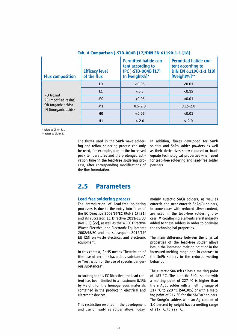
In the production of electronic assemblies, flux systems are used which have to be cleaned (cleanable) or not cleaned (no-clean) after soldering.
For the classification of fluxes, the IPC J-STD-004 [20] and the DIN EN 61190-1-1 [18] are standardly used.
In IPC J-STD-004B [17] (Table 3-2 "Test Requirements for Flux Classification"), the no-clean state means that the classified flux must pass the SIR (Surface Insulation Resist-ance) and ECM (Electrochemical Migration) test in the unclean state after soldering. This means that the test samples loaded with the flux to be tested are not cleaned (no-clean) prior to the SIR and ECM tests. After the SIR test has been completed, the surface insula-tion resistance of the test samples is at least 100 MΩ and the test criteria must be met to pass the ECM test.
The SIR test, including the pre-treatment and preparation of the test samples with the flux according to IPC J-STD-004B [17] (item 3.4.1.4), is carried out in the IPC-TM650 [19] (Test Methods Manual, point 2.6.3.7) and the ECM test in the IPC-TM650 [19] (Test Methods Manual, point 2.6.14.1).
DIN EN 61190-1-1:2003 describes the test requirements for the classification of the flux activity. In the case of no-clean fluxes, their residues may only be tested in the unclean state. It should be noted here that the sample with the flux is subjected to a thermal load before the SIR test with the prescribed soldering process.
If an assembly for which a no-clean flux is used is to be cleaned before applying pro-tective coatings, the user should check the SIR values after cleaning. The requirements for the surface insula-tion of fluxes for the satisfaction of the 100-MΩ-SIR requirements of DIN EN 61190-1-1:2003 must be determined in accordance with test method 5E01 of the standard DIN EN 61189-5:2006.
The SIR test is used to characterise fluxes in accordance with DIN EN 61189-5:2007 by determining the drop in the electrical insulation resistance of test samples from rigid Printed Circuit Board (PCB) through the action of a specific flux. This test is carried out under high humidity and under heat stress in climatic chambers.
* The definition of rework and repair according to ECSS is different from the IPC definition. In this guide the IPC definition is used (see Glossary).
2.4 Flux interaction "No-clean - but..."
Document Document name Main contents
ECSS-Q-ST-70-38 [15] High-reliability soldering for surface-mount and mixed technology
• Specifications for pro-cedures, materials and temperatures of SMD soldering and repair processes*
• Drying of printed circuit boards
IGF 15.535N [16] Resistance to soldering and reliability of new designs in the manual repair process of leadless electronic assemblies
• Recommendations of pro-cedures and temperatures for manual SMD and THT soldering and rework and repair processes
• Workmanship• Stencils for
work instructions• Reliability studies
Tab. 2: Overview of the rules

13
1 Fluxes are available in solid (S), pasty/creamy (P) or liquid (L) form.2 0 and 1 indicate the absence or presence of halides. See 4.2.3 for an explanation of the classification of L, M and H.3 See 7.2 and 7.3 for the comparison of the composition classes RO, RE, OR and IN as well as the efficacy levels L, M and H with the conventional classes such as R, RMA, RA, water-soluble and low-solid species which do not require subsequent purification (no-clean).4 ISO designations, with the exception of small feature deviations, are similar to the IEC designations.
Tab. 3: Table EN 61190-1-1
No-clean is a product-specific and isolated property of flux residues. Secure compat-ibility with other no-clean products as well as with not explicitly specified cleaning media is not guaranteed.
Please note the following in the rework pro-cess:
The no-clean properties apply only to flux residues which have experienced the solder-ing process (thermal load) which is intended for them. Separate evidence (SIR/ECM) must be provided for areas which have not been sufficiently heated.
Substances contained in the composition oftheflux1
Efficacylevels oftheflux (wt. % halide) 2
Description oftheflux according to IEC3
Description ofthefluxaccording to ISO4
Rosin(RO)
Low (<0.01) L0 Low (<0.15) L1Moderate (<0.01) M0Moderate (0.15-2.0) M1High (<0.01) H0High (> 2.0) H1
ROL0ROL1ROM0ROM1ROH0ROH1
1.1.11.1.2.W, 1.1.2.Z1.1.31.1.2.Y, 1.1.2.Z1.1.3.X1.1.2.Z
Resin(RE)
Low (<0.01) L0 Low (<0.15) L1Moderate (<0.01) M0Moderate (0.15-2.0) M1High (<0.01) H0High (> 2.0) H1
REL0REL1REM0REM1REH0REH1
1.2.11.2.2.W, 1.2.2.X1.2.3.W1.2.2.Y, 1.2.2.Z1.2.3.X1.2.2.Z
Organic(OR)
Low (<0.01) L0 Low (<0.15) L1Moderate (<0.01) M0Moderate (0.15-2.0) M1High (<0.01) H0High (> 2.0) H1
ORL0ORL1ORM0ORM1ORH0ORH1
2.1, 2.2.3.E--2.1.2, 2.2.22.2.3.02.2.2
Inorganic(IN)
Low (<0.01) L0 Low (<0.15) L1Moderate (<0.01) M0Moderate (0.15-2.0) M1High (<0.01) H0High (> 2.0) H1
INL0INL1INM0INM1INH0INH1
Not applicable(inorganic ISO flux is procured elsewhere)
14
Flux compositionEfficacylevel oftheflux
Permitted halide con-tent according to IPC J-STD-004B [17] In [weight%]*
Permitted halide con-tent according to DIN EN 61190-1-1 [18][Weight%]**
RO (rosin)RE (modified resins)OR (organic acids)IN (inorganic acids)
L0 <0.05 <0.01
L1 <0.5 <0.15
M0 <0.05 <0.01
M1 0.5-2.0 0.15-2.0
H0 <0.05 <0.01
H1 > 2.0 > 2.0
* refers to Cl, Br, F, I.
** refers to Cl, Br, F.
Tab. 4 Comparison J-STD-004B [17]/DIN EN 61190-1-1 [18]
2.5 Parameters
Lead-free soldering process The introduction of lead-free soldering processes is due to the entry into force of the EC Directive 2002/95/EC (RoHS 1) [21] and its successor, EC Directive 2011/65/EU (RoHS 2) [22], as well as the WEEE Directive (Waste Electrical and Electronic Equipment) 2002/96/EC and the subsequent 2012/19/EU [23] on waste electrical and electronic equipment.
In this context, RoHS means "Restriction of (the use of certain) hazardous substances" or "restriction of the use of specific danger-ous substances".
According to this EC Directive, the lead con-tent has been limited to a maximum 0.1% by weight for the homogeneous materials contained in the product in electrical and electronic devices.
This restriction resulted in the development and use of lead-free solder alloys. Today,
mainly eutectic SnCu solders, as well as eutectic and near-eutectic SnAgCu solders, in some cases with reduced silver content, are used in the lead-free soldering pro-cess. Microalloying elements are standardly added to these solders in order to optimise the technological properties.
The main difference between the physical properties of the lead-free solder alloys lies in the increased melting point or in the increased melting range and in contrast to the SnPb solders in the reduced wetting behaviour.
The eutectic Sn63Pb37 has a melting point of 183 °C. The eutectic SnCu solder with a melting point of 227 °C is higher than the SnAgCu solder with a melting range of 217 °C to 220 °C (SAC305) or with a melt-ing point of 217 °C for the SAC387 solders. The SnAgCu solders with an Ag content of 1.0 percent by weight have a melting range of 217 °C. to 227 °C.
The fluxes used in the SnPb wave solder-ing and reflow soldering process can only be used, for example, due to the increased peak temperatures and the prolonged acti-vation time in the lead-free soldering pro-cess, after corresponding modifications of the flux formulation.
In addition, fluxes developed for SnPb solders and SnPb solder powders as well as their derivatives show reduced or inad-equate technological properties when used for lead-free soldering and lead-free solder powders.

15
Tab. 5: Overview of typical solder alloys
The increased melting temperatures (com-pared to SnPb solders, see Figure 2) of the lead-free solder alloys are reflected in the temperature/time profile using the example of the SnAgCu reflow profile according to DIN EN 61760-1:2006 (see Figure 3). In addition, the prolonged pre-heating times
and thus activation times for the fluxes are evident.
DesignationAlloy/Composition [%]
Melting temperature [°C]
AuSn Au80 Sn20 280
SC Sn99.3 Cu0.7 227
SnAg Sn96.5 Ag3.5 221
SAC105 Sn98.5 Ag1.0 Cu0.5 217-227
SAC387 Sn95.5 Ag3.8 Cu0.7 217
SAC305 Sn96.5 Ag3.0 Cu0.5 214-220
Innolot Sn90.95 Ag3.8 Cu0.7 Bi3.0 Sb1.4 Ni0.15
206-218
SnPb Sn63 Pb37 183
SnPbAg Sn62 Pb36 Ag2 179
BiSn Bi58 Sn42 139
Fig. 2: Solder profile for SnPb solder according to DIN EN 61760-1
0 20 40 60 80 100 120 140 160 180 200 220 240
Source: DIN EN 61760-1
300
250
200
150
100
50
0
130 °C
150 °C
160 °C180 °C
215 °C230 °C
240 °C
Preheating Approx. 60 s >180 °C
Cooling rate <6 K/s
SnPb melting
Typical Heating rate <3 K/s
Time (sec)
Tem
pera
ture
(°C
)
16
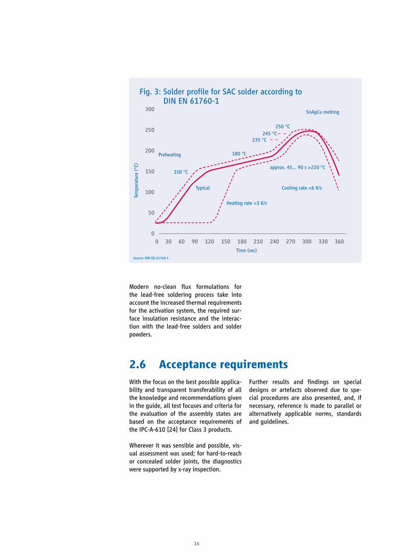
Modern no-clean flux formulations for the lead-free soldering process take into account the increased thermal requirements for the activation system, the required sur-face insulation resistance and the interac-tion with the lead-free solders and solder powders.
Fig. 3: Solder profile for SAC solder according to DIN EN 61760-1
0 30 60 90 120 150 180 210 240 270 300 330 360
Source: DIN EN 61760-1
300
250
200
150
100
50
0
180 °C
150 °C
235 °C245 °C
250 °C
Preheating
approx. 45... 90 s >220 °C
Cooling rate <6 K/s
SnAgCu melting
Typical
Heating rate <3 K/s
Time (sec)
Tem
pera
ture
(°C
)
2.6 Acceptance requirementsWith the focus on the best possible applica-bility and transparent transferability of all the knowledge and recommendations given in the guide, all test focuses and criteria for the evaluation of the assembly states are based on the acceptance requirements of the IPC-A-610 [24] for Class 3 products.
Wherever it was sensible and possible, vis-ual assessment was used; for hard-to-reach or concealed solder joints, the diagnostics were supported by x-ray inspection.
Further results and findings on special designs or artefacts observed due to spe-cial procedures are also presented, and, if necessary, reference is made to parallel or alternatively applicable norms, standards and guidelines.

17
2.7 Printed circuit boardIn addition to the basic need of tempera- ture resistance of the printed circuit board during lead-free soldering process, the question of the thermal stress of the printed circuit board in the application must also be clarified before a base material for the printed circuit board is selected.
Various base material parameters which could be helpful for selection are briefly presented below. Finally, the question is raised whether there are any corresponding parameters for the base material and what they look like for different materials.
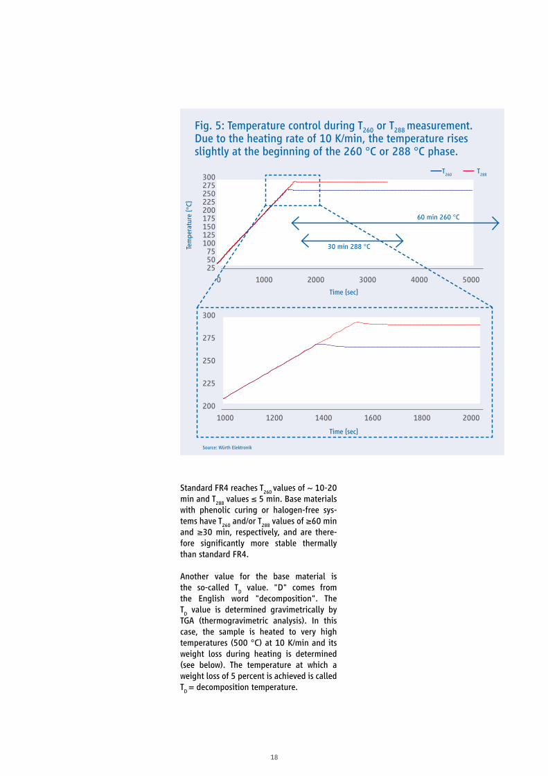
The first thing to mention here is the so-called T260/T288 value. In order to deter-mine this value for a material, a corre-sponding TMA measurement is carried out. Thermomechanical analysis (TMA) is a method in which the expansion of a mate-rial as a function of temperature is meas-ured under a defined load. The measure-ment setup is briefly shown in the following figure.
To accommodate the expansion of the entire circuit board samples with the ball head, it is placed between two quartz platelets in the measuring transducer (see above). The expansion of the quartz platelets (~ 1.5-1.7ppm/°C or ~ 0.5μm over the temperature range considered here) is negligible.
The sample is here heated to 10 °C/min to 260 °C/288 °C and then left at this tem-perature for 60 min/30 min. The time from reaching the 260 °C/288 °C mark, up to the first delamination (irreversible z-axis expansion/jump) must then be measured from the recorded z-axis expansion curve (see below). The measured time then cor-responds to the T
260/T
288 value.
Source: Würth Elektronik
Fig. 4: TMA measuring device (left). Sensor with ball head (right). The sample can be heated up or cooled by means of gas cooling in the measuring chamber. During the entire measurement, a predefined force is applied to the sensor (typically 5-20 g).
Measuring chamber
Measuring sensor with ball head
Quartz platelets
Glass table
Circuit boardsample
Temperature sensor
18
Standard FR4 reaches T260
values of ~ 10-20 min and T
288 values ≤ 5 min. Base materials
with phenolic curing or halogen-free sys-tems have T
260 and/or T
288 values of ≥60 min
and ≥30 min, respectively, and are there-fore significantly more stable thermally than standard FR4.
Another value for the base material is the so-called T
D value. "D" comes from
the English word "decomposition". The T
D value is determined gravimetrically by
TGA (thermogravimetric analysis). In this case, the sample is heated to very high temperatures (500 °C) at 10 K/min and its weight loss during heating is determined (see below). The temperature at which a weight loss of 5 percent is achieved is called T
D = decomposition temperature.
Fig. 5: Temperature control during T260 or T288 measurement. Due to the heating rate of 10 K/min, the temperature rises slightly at the beginning of the 260 °C or 288 °C phase.
0 1000 2000 3000 4000 5000
1000 1200 1400 1600 1800 2000
Source: Würth Elektronik
300275250225200175150125100755025
300
275
250
225
200
T260
T288
Time {sec}
Time {sec}
255075
100125150175200225250275300
0 1000 2000 3000 4000 5000
t [sec]
T [°C]
T260 T288
200
225
250
275
300
1000 1200 1400 1600 1800 2000
t [sec]
T [°C]
T260 T288
255075
100125150175200225250275300
0 1000 2000 3000 4000 5000
t [sec]
T [°C]
T260 T288
200
225
250
275
300
1000 1200 1400 1600 1800 2000
t [sec]
T [°C]
T260 T288
255075
100125150175200225250275300
0 1000 2000 3000 4000 5000
t [sec]
T [°C]
T260 T288
200
225
250
275
300
1000 1200 1400 1600 1800 2000
t [sec]
T [°C]
T260 T288
255075
100125150175200225250275300
0 1000 2000 3000 4000 5000
t [sec]
T [°C]
T260 T288
200
225
250
275
300
1000 1200 1400 1600 1800 2000
t [sec]
T [°C]
T260 T288
60 min 260 °C
30 min 288 °CTem
pera
ture
{°C
}

19
Fig. 6: Evaluation of the T288 values / times. In the examples shown, sample 1 reaches a T288 value of >/=30 min (total measurement time) and sample 2 reaches a value of T288 = 1 min. 40 sec.
0 500 1000 1500 2000 2500 3000
1400 1450 1500 1550 1600 1650 1700
1400 1600 1800 2000 2200 2400 2600 2800 3000 3200
Source: Würth Elektronik
Sample 1 Sample 2
90
80
70
60
50
40
30
20
10
0
85
83
81
79
77
75
73
71
69
67
65
85
80
75
70
65
60
55
50
45
40
Time {sec}
Time {sec}
Time {sec}
0
10
20
30
40
50
60
70
80
90
0 500 1000 1500 2000 2500 3000
t [se c]
z-Achsenausdehnung [µm]
M uster 1 M uster 2
40
45
50
55
60
65
70
75
80
85
1400 1600 1800 2000 2200 2400 2600 2800 3000 3200
t [sec]
z-Achsenausdehnung [µm]
Muster 1 Muster 2
100sec
1800sec
65
67
69
71
73
75
77
79
81
83
85
1400 1450 1500 1550 1600 1650 1700
t [se c ]
z-Achsenausdehnung [µm]
M u s te r 1 M u s te r 2
Z-ax
is e
xpan
sion
{μm
}Z-
axis
exp
ansi
on {
μm}
Z-ax
is e
xpan
sion
{μm
}
0
10
20
30
40
50
60
70
80
90
0 500 1000 1500 2000 2500 3000
t [se c]
z-Achsenausdehnung [µm]
M uster 1 M uster 2
40
45
50
55
60
65
70
75
80
85
1400 1600 1800 2000 2200 2400 2600 2800 3000 3200
t [sec]
z-Achsenausdehnung [µm]
Muster 1 Muster 2
100sec
1800sec
65
67
69
71
73
75
77
79
81
83
85
1400 1450 1500 1550 1600 1650 1700
t [se c ]
z-Achsenausdehnung [µm]
M u s te r 1 M u s te r 2
100 sec
1800 sec
Delamination(Irreversible expansion in the z-axis)

20
If the decomposition temperature is reached or exceeded, the base material is destroyed irreversibly. The T
D value for standard FR4
is in the range of ~ 310 °C. At tempera-tures above 310 °C, FR4 is thus irrevoca-bly destroyed. Standard high-T
G materials
(DICY, hardened as standard FR4) show no advantages with respect to the two values T
D and T
260/288
. Base materials with phenolic
curing or halogen-free systems have signifi-cantly higher T
D values (≥340 °C.). There are
now base materials with TD values of 400 °C.
Fig. 7: Example of TGA measurement. The temperature at which a weight loss of 5 percent is achieved is called T
D = decomposi-
tion temperature.
50 100 150 200 250 300 350 400 450 500
105
100
95
90
85
80
75
Temperature {°C}
Wei
ght
{%}
Source: Würth Elektronik
Fig. 8: Overview of different materials using the T260
and TD val-ues. The halogen-free and phenolic (novolak) annealed systems have significantly higher thermal load bearing capacity.
15 30 45 60
370
360
350
340
330
320
310
300
T260
{min} Time to delamination @260 °C
T D {
°C}
deco
mpo
siti
on t
empe
ratu
re
Source: Würth Elektronik
DICY
Standard FR4
Novolakhalogen-free
21
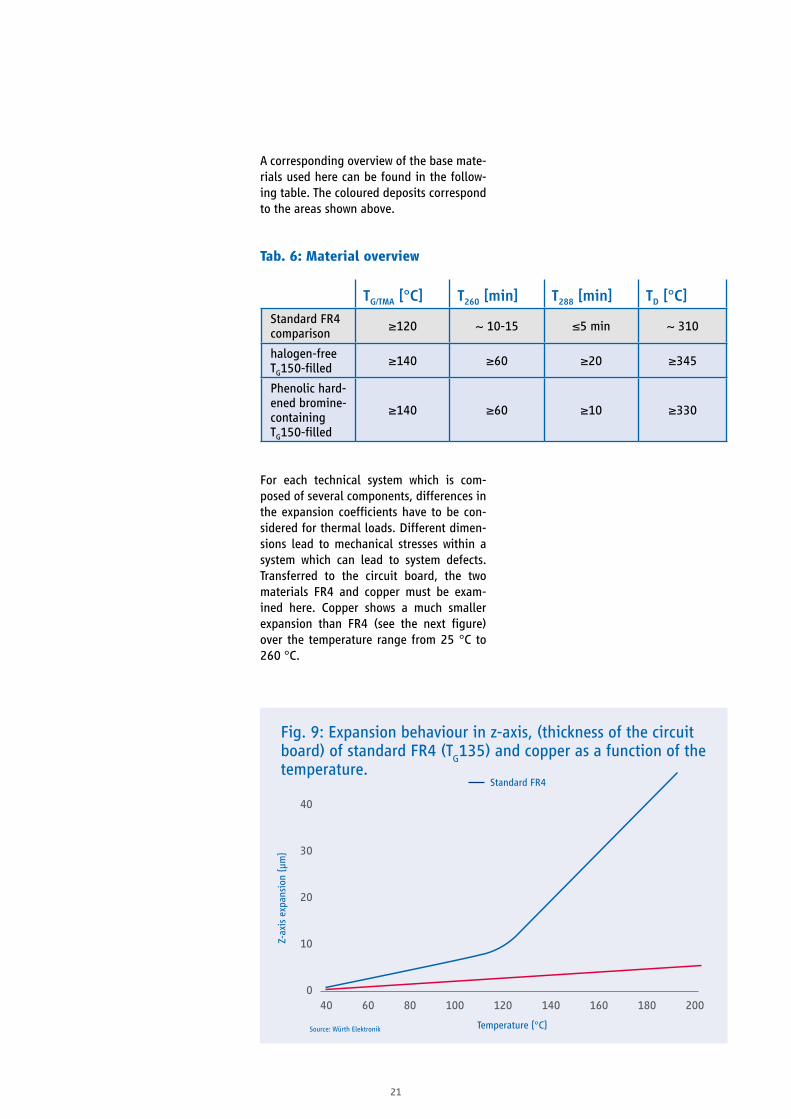
A corresponding overview of the base mate-rials used here can be found in the follow-ing table. The coloured deposits correspond to the areas shown above.
For each technical system which is com-posed of several components, differences in the expansion coefficients have to be con-sidered for thermal loads. Different dimen-sions lead to mechanical stresses within a system which can lead to system defects. Transferred to the circuit board, the two materials FR4 and copper must be exam-ined here. Copper shows a much smaller expansion than FR4 (see the next figure) over the temperature range from 25 °C to 260 °C.
TG/TMA [°C] T260 [min] T288 [min] TD [°C]
Standard FR4 comparison ≥120 ~ 10-15 ≤5 min ~ 310
halogen-free TG150-filled ≥140 ≥60 ≥20 ≥345
Phenolic hard-ened bromine-containing TG150-filled
≥140 ≥60 ≥10 ≥330
Tab. 6: Material overview
Fig. 9: Expansion behaviour in z-axis, (thickness of the circuit board) of standard FR4 (T
G135) and copper as a function of the
temperature.
40 60 80 100 120 140 160 180 200
40
30
20
10
0
Temperature {°C}Source: Würth Elektronik
Z-ax
is e
xpan
sion
{μm
}
Standard FR4
22
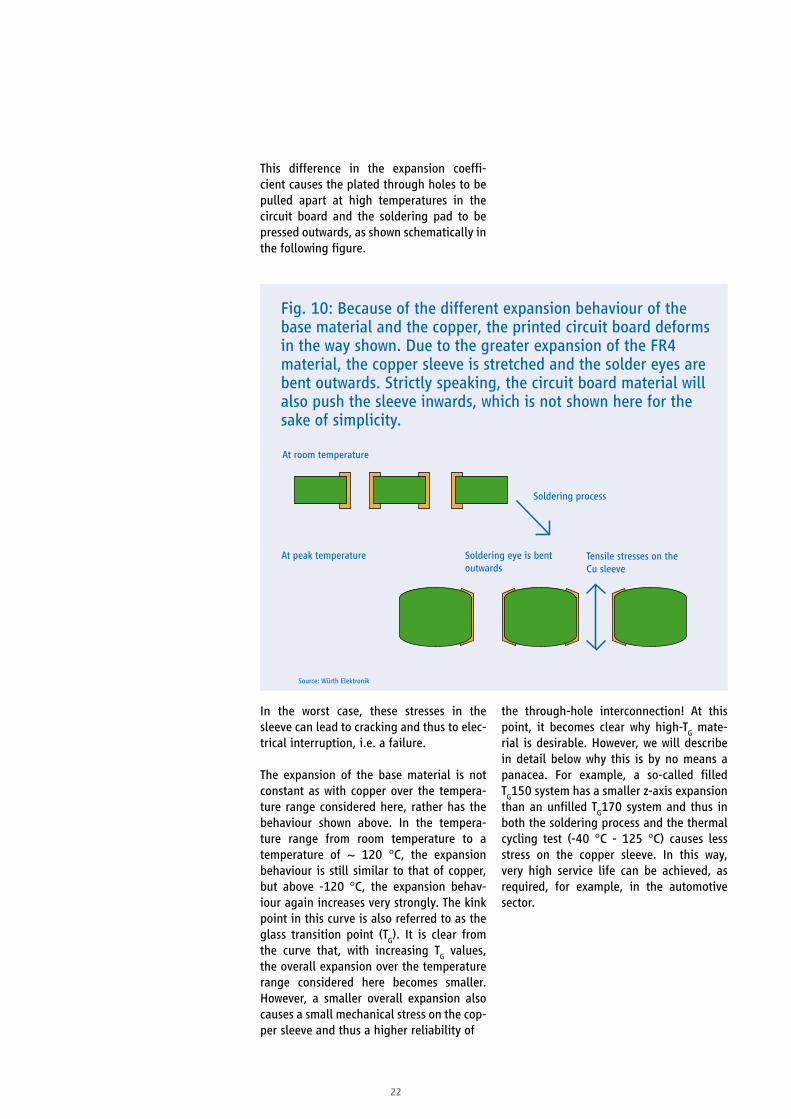
This difference in the expansion coeffi-cient causes the plated through holes to be pulled apart at high temperatures in the circuit board and the soldering pad to be pressed outwards, as shown schematically in the following figure.
In the worst case, these stresses in the sleeve can lead to cracking and thus to elec-trical interruption, i.e. a failure.
The expansion of the base material is not constant as with copper over the tempera-ture range considered here, rather has the behaviour shown above. In the tempera-ture range from room temperature to a temperature of ~ 120 °C, the expansion behaviour is still similar to that of copper, but above -120 °C, the expansion behav-iour again increases very strongly. The kink point in this curve is also referred to as the glass transition point (T
G). It is clear from
the curve that, with increasing TG values,
the overall expansion over the temperature range considered here becomes smaller. However, a smaller overall expansion also causes a small mechanical stress on the cop-per sleeve and thus a higher reliability of
the through-hole interconnection! At this point, it becomes clear why high-T
G mate-
rial is desirable. However, we will describe in detail below why this is by no means a panacea. For example, a so-called filled T
G150 system has a smaller z-axis expansion
than an unfilled TG170 system and thus in
both the soldering process and the thermal cycling test (-40 °C - 125 °C) causes less stress on the copper sleeve. In this way, very high service life can be achieved, as required, for example, in the automotive sector.
Fig. 10: Because of the different expansion behaviour of the base material and the copper, the printed circuit board deforms in the way shown. Due to the greater expansion of the FR4 material, the copper sleeve is stretched and the solder eyes are bent outwards. Strictly speaking, the circuit board material will also push the sleeve inwards, which is not shown here for the sake of simplicity.
Source: Würth Elektronik
At room temperature
At peak temperature
Soldering process
Soldering eye is bent outwards
Tensile stresses on the Cu sleeve

23
Fig. 11: z-axis expansion as a function of temperature of a circuit board type, built with different base materials (standard FR4 is always unfilled!). The filled T
G150 system has the small-
est expansion values in all areas.
40 90 140 190
40
35
30
25
20
15
10
5
0
Temperature {°C}Source: Würth Elektronik
z-ax
is e
xpan
sion
{μm
}Standard FR4
TG150 HF-filled
340 ppm/°C280 ppm/°C
205 ppm/°C
41 ppm/°C
70 ppm/°C 70 ppm/°CT
G 120 °C
TG 170 °C
TG 150 °C
TG170 unfilled
Fig. 12: Comparison of total z-axis expansions of the materials shown above in different temperature ranges. On the left the comparison of total expansion of the printed circuit board from room temperature (RT) to peak temperature with lead-free sol-dering of 260 °C, and right for temperature cycling tests in the range (-40 °C... 125 °C). In both cases, the lowest values are obtained with the filled T
G150 system, that is, in both cases, it
is an improvement on the printed circuit board reliability.
70
60
50
40
30
20
10
0
RT... 260 °C -40 °C... +125 °C
Source: Würth Elektronik
Z-ax
is e
xpan
sion
{μm
}
Standard FR4
TG150 HF-filled T
G170 unfilled
24
The above parameters are important for reliability requirements in the application of the assembly and the resulting require-ments for the base material of the printed circuit board. On the other hand, it must
also be considered that other mechani-cal parameters can play a decisive role. If, for example, press-fit connectors are used in an assembly in addition to sol-dered components, the mechanical
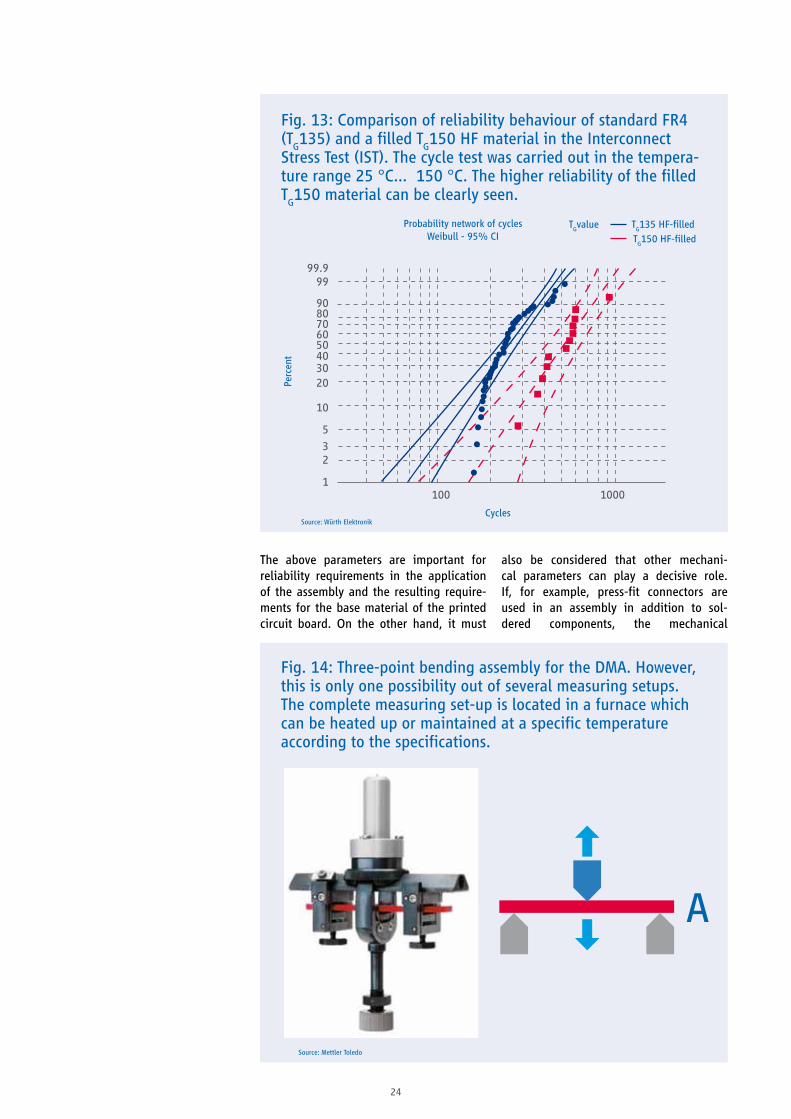
Fig. 13: Comparison of reliability behaviour of standard FR4 (T
G135) and a filled T
G150 HF material in the Interconnect
Stress Test (IST). The cycle test was carried out in the tempera-ture range 25 °C... 150 °C. The higher reliability of the filled T
G150 material can be clearly seen.
CyclesSource: Würth Elektronik
Perc
ent
TGvalueProbability network of cycles
Weibull - 95% CIT
G135 HF-filled
TG150 HF-filled
Fig. 14: Three-point bending assembly for the DMA. However, this is only one possibility out of several measuring setups. The complete measuring set-up is located in a furnace which can be heated up or maintained at a specific temperature according to the specifications.
Source: Mettler Toledo
A
100 1000
99.999
9080706050403020
10
5
32
1
25
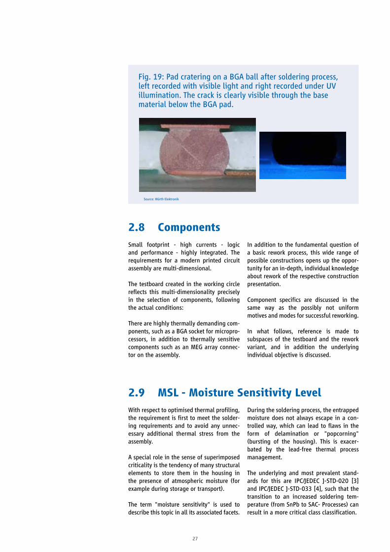
strength (modulus of elasticity) of a material in the temperature range must also be considered in the application. Base materials exhibit the effect of becom-ing "soft" at high temperatures (in the region of the glass transition point) which would lead to increased transitional resist-ances and possibly failure in press-fit con-tacts. The modulus of elasticity can be determined by means of DMA (dynamic mechanical analysis) (see Figure 15).
Another property that must be considered for the reliability of an assembly under extreme environmental conditions, in par-ticular high temperature and high humidity,
is the behaviour of the base material with respect to CAF. CAF (Conductive Anodic Fila-mentation) means the formation of copper filaments in the base material which grow from the anode to the cathode (see Figure 16). If the copper filament reaches the cath-ode, a short circuit is produced between the two poles (as shown in the measuring dia-gram shown below). A comparison of stand-ard FR4 (DICY-annealed) with phenolically hardened or halogen-free systems shows that standard FR4 is significantly worse with regard to CAF!
Fig. 16: Under the influence of electric fields (voltages), copper filaments can form in the printed circuit board at high atmos-pheric humidity, the filaments starting from the anode and growing in the direction of the cathode. This effect is called CAF.
Fig. 15: DMA measurements of two filled base materials, measured by the three-point bending test. In the range of the glass transition temperature, the modulus of elasticity drops sharply.
50 100 150 200 250
18
16
14
12
10
8
6
4
2
Temperature {°C}
Peer
mod
ulus
E {
GPa
}
Cavity-free TG150 Bromine-containing T
G150
Source: Würth Elektronik
Source: Würth Elektronik Source: ZVEI

26
Although the filled, phenolic annealed and halogen free materials have some advan-tages in thermal as well as CAF resistance, they are more brittle than standard FR4 and have lower copper adhesion. This is espe-cially the case with the filled systems. The typical copper adhesion in filled systems is about 30 percent lower than in standard FR4.
The higher brittleness is also evident in the case of effects such as so-called pad crater-ing. Due to the increased brittleness of the base material, the soldering process can lead to cracking in the base material due to deformation of the components or the cir-cuit board (see Figure 19).
Fig. 18: Copper strength of a 35 μm copper foil on different base materials. Phenolically hardened or halogen-free filled systems have an approx. 30% lower copper adhesion than standard FR4.
Source: Würth Elektronik
1.9
1.7
1.5
1.3
1.1
0.9
0.7
Standard FR4 Filled system
Type
-Cu
Adhe
sive
str
engt
h {N
7mm
}
Fig. 17: CAF measurement at 85 °C, 85 percent relative humid-ity and 100 V applied voltage. The borehole spacing consid-ered here was 400 μm (pitch 700 μm, tool diameter 300 μm). The limit of the resistance to 1 MΩ is determined by the built-in series resistor which should also prevent the filament from burning off.
Source: Würth Elektronik
0 200 400 600 800 1000
10
9
8
7
6
5
4
3
2
1
T {h}
Log 10
R {Ω
}
27
2.8 ComponentsSmall footprint - high currents - logic and performance - highly integrated. The requirements for a modern printed circuit assembly are multi-dimensional.
The testboard created in the working circle reflects this multi-dimensionality precisely in the selection of components, following the actual conditions:
There are highly thermally demanding com-ponents, such as a BGA socket for micropro-cessors, in addition to thermally sensitive components such as an MEG array connec-tor on the assembly.
In addition to the fundamental question of a basic rework process, this wide range of possible constructions opens up the oppor-tunity for an in-depth, individual knowledge about rework of the respective construction presentation.
Component specifics are discussed in the same way as the possibly not uniform motives and modes for successful reworking.
In what follows, reference is made to subspaces of the testboard and the rework variant, and in addition the underlying individual objective is discussed.
Fig. 19: Pad cratering on a BGA ball after soldering process, left recorded with visible light and right recorded under UV illumination. The crack is clearly visible through the base material below the BGA pad.
Source: Würth Elektronik
2.9 MSL - Moisture Sensitivity LevelWith respect to optimised thermal profiling, the requirement is first to meet the solder-ing requirements and to avoid any unnec-essary additional thermal stress from the assembly.
A special role in the sense of superimposed criticality is the tendency of many structural elements to store them in the housing in the presence of atmospheric moisture (for example during storage or transport).
The term "moisture sensitivity" is used to describe this topic in all its associated facets.
During the soldering process, the entrapped moisture does not always escape in a con-trolled way, which can lead to flaws in the form of delamination or "popcorning" (bursting of the housing). This is exacer-bated by the lead-free thermal process management.
The underlying and most prevalent stand-ards for this are IPC/JEDEC J-STD-020 [3] and IPC/JEDEC J-STD-033 [4], such that the transition to an increased soldering tem-perature (from SnPb to SAC- Processes) can result in a more critical class classification.

28
Against the background of the reworking, there may be a conflict with regard to the permitted time corridor (see Table 7: Over-view of MSL classification according to J-STD-020 [3]).
Note:• In any case of doubt, the assembly must
be dried back immediately before the rework measure, since the moisture his-tory of the affected assembly is often not known reliably or sufficiently for uncon-trolled moisture absorption.
• In the broadest sense, the printed circuit board is also a moisture-sensitive compo-nent (but without MSL classification).
Table7:OverviewMSLclassificationaccordingtoJ-STD-020[3]
Table 5-1 Moisture Sensitivity Classes
ClassComponent dwell time
Requirements for moisture absorption
Standard
Accelerated equivalent 1
eV 0.40-0.48
eV 0.30-0.39
Conditions
Time Conditions Time (hours) Conditions Time
(hours)Time (hours)
1 Unlimited ≤30 °C/85%
relative moisture
168 +5/-085 °C/85%
relative moisture
Not applicable
Not applicable
Not applicable
2 1 year ≤30 °C/60 %
relative moisture
168 +5/-085 °C/60 %
relative moisture
Not applicable
Not applicable
Not applicable
2a 4 weeks ≤30 °C/60 %
relative moisture
6962 +5/-030 °C/60 %
relative moisture
120 +1/-0 168 +1/-060 °C/60 %
relative moisture
3 168 hours≤30 °C/60 %
relative moisture
1922 +5/-030 °C/60 %
relative moisture
40 +1/-0 52 +1/-060 °C/60 %
relative moisture
4 72 hours≤30 °C/60 %
relative moisture
962 +2/-030 °C/60 %
relative moisture
20 +0.5/-0 24 +0.5/-060 °C/60 %
relative moisture
5 48 hours≤30 °C/60 %
relative moisture
722 +2/-030 °C/60 %
relative moisture
15 +0.5/-0 20 +0.5/-060 °C/60 %
relative moisture
5a 24 hours≤30 °C/60 %
relative moisture
482 +2/-030 °C/60 %
relative moisture
10 +0.5/-0 13 +0.5/-060 °C/60 %
relative moisture
6
Time according to label (Time on label TOL)
≤30 °C/60% relative moisture
TOL 30 °C/60 %
relative moisture
Not applicable
Not applicable
Not applicable
Note 1: ATTENTION - The requirements for moisture absorption under the accelerated equivalent must not be applied until the correlation of the damaging effect (including electrical damage) after the moisture absorption and reflow has been determined according to the standard moisture absorption requirements or the known diffu-sion activation energy of the housing material in the ranges 0.4-0.48 eV and 0.3-0.39 eV, respectively. The times of the accelerated moisture absorption can vary depending on the material properties (e.g. injection moulding compound, encapsulation, etc.). The JEDEC document JESD22-A120 contains a method for determin-ing the diffusion coefficient.
Note 2: The standard moisture absorption time takes into account a default value of 24 hours for the manufacturer's exposure time (MET) between the annealing and the packaging in damp-proof bags. The maximum permitted time that the components spend outside the bag at the distributor is included. If the actual MET is less than 24 hours, the moisture absorption time can be reduced. For moisture absorption conditions of 30 °C/60% relative humidity, the moisture absorption time is reduced by 1 hour for each hour that the MET is less than 24 hours. For moisture absorption conditions of 60 °C/60% relative humidity, the moisture absorption time is reduced by 1 hour for each 5-hour block that the MET is under 24 hours. If the actual MET is over 24 hours, the moisture absorption time must be increased. For a humidity absorption of 30 °C/60% relative humidity, the moisture absorption time is increased by 1 hour for each hour in which the MET is over 24 hours. For a humidity absorption of 60 °C/60% relative humidity, the moisture absorption time is increased by 1 hour for each 5-hour block which is the MET over 24 hours.
Note 3: The supplier can increase the moisture absorption time at his own risk.

29
2.10 Thermalprofiling2.10.1 Tools and Sensor positioningA multichannel measuring transducer (consisting of a separate transmitting and receiving unit including software) and cali-brated NiCr-Ni thermocouples (type K) are typically used for the temperature meas-urement. In the best case, the temperature measuring system and thermocouples are calibrated as a unit, but at the minimum they should be calibrated separately. For the temperature measuring system, regular maintenance including recalibration and the classification as measuring equipment in the QM system are recommended.
Shell thermocouples of accuracy class 1 with an outer diameter of 0.25 mm have proven to be effective. Due to their measuring char-acteristics and their low heat capacity, they provide fast and precise measurement data. The precondition, however, is the proper assembly of the thermocouples. The lead is fixed, for example, with a small amount of SMD adhesive or polyimide adhesive tape on the printed circuit board. The sensor is contacted with aluminium tape or small amounts of thermal paste and polyimide adhesive tape. A solid and secure thermal contact between the sensor and the meas-uring object which is maintained over the entire measurement provides the basis for successful temperature measurement.
The application of the temperature sensors determines the quality of the measurement. Incorrect assembly can lead to considerable faults with impermissible deviations. The reason for this is, for example, shading of convection, excessive heat capacity of the measuring point or inadequate contact with the measuring object.
The soldering process is to be measured at soldering points (also at concealed solder-ing points, here, if necessary, by means of a CNC drilling machine, to drill the solder-ing point from below, see IPC-7095 [6]). In order to monitor compliance with limit tem-peratures, temperature-sensitive compo-nents or exposed positions on the assembly are measured. Areas of minimum and maxi-mum thermal mass are taken into account.
2.10.2 Methodology of profiledeterminationThe solder profile used in the series process serves as the basis for the rework solder profile. Since, during reworking, "only" the component to be reworked must reach the soldering temperature, a shorter solder pro-file which satisfies the component require-ments can also be used, taking into account the limiting parameters.
The following basic work steps serve as the main thread for the profile determination. Depending on the rework system used (or manual soldering station used in the case of manual soldering), this results in device-specific sequences which are described in detail in sections 2.14 ff.
Basic steps for profile creation on a test assembly:
1. Setting a parameter set Do not set the target temperature too
high in order to avoid damage (e.g. conductor plate delamination)
2. Working out a temperature profile in the process window
The specifications are based on line pro-cess, norms/standards, data sheet for the soldering material, restrictions on LP and component manufacturers
3. Test of the measurement setup to exclude systematic measurement faults
4. Performance of a temperature measure-ment and process qualification
Check the plausibility of the results5. Retraction of the solder profile with a
view to a stable process This should ideally be located in the
middle of the process window6. Verification of the solder quality on a test
assembly7. Monitoring of the rework system (the
manual soldering system), through ongoing process and device control
The soldering and solder profile is almost identical to the solder profile in the inline reflow process. Since the rework tempera-ture-time profile in the postprocessing pro-cess must be optimised only for one compo-nent, it may possibly be slightly colder and shorter than the inline profile. Recommen-dations can be found on this, for example, in IPC-7095 [6] (processing of BGAs).

30
With a large-area under-heating system which heats the entire assembly, the major-ity of the required heat energy should be introduced from below, so that only the required "residual heat" needs to be intro-duced to the component via the upper heat-ing system up to the maximum tempera-ture. This significantly reduces the risk of overheating the component. Attention must be paid to the thermal protection of tem-perature-sensitive adjacent components.
The circuit board temperature on the upper side should be suitable for soldering of SAC alloys at at least 140-160 °C, in order to achieve uniform heating and to avoid local overheating. Different stretching behaviour of cool, rigid circuit board areas in direct proximity to hot, soft (heated over T
G) LP
areas can cause mechanical stresses.
The consequences may be sleeve cracks, delaminations or other defects.
In general, the following applies:• If component temperatures (component
type J-STD-033 [4]) above 200 °C are reached during the reworking process, the entire assembly must be re-dried before starting the rework.
• Moisture-sensitive SMD housing must at no time exceed the characteristics of its moisture-sensitive class according to J-STD-020 [3].
• According to J-STD-033 [4], the compo-nents/assembly are preferably dried at 125 °C in the circulating furnace. In the presence of temperature-sensitive com-ponents, drying can also be carried out at lower temperatures and lower relative humidity.
• The solder heat resistance of all compo-nents on the assembly must be observed.
• Component temperatures are measured on the top side of the component in the centre of the housing.
In what follows, profile creation and process qualification will be shown by way of the example of a BGA256.
Fig. 20: Positioning of thermocouples, PCB top
Source: Fraunhofer ISIT
TE2
TE1

31
Figure 20 and Figure 21 show the position-ing of the thermocouples to measure the temperatures at the relevant measuring points.
Figure 22 shows the measurement in the concealed BGA solder joints. Thermocouple 5 is located in the middle of the printed cir-cuit board and is not visible in the image sections.
Fig. 21: Positioning of thermocouples, PCB bottom
Source: Fraunhofer ISIT
TE4
TE3
TE6
TE7
Fig. 22: Positioning of the thermocouples in concealed solder joints
Source: Fraunhofer ISIT
TE6
TE7
32
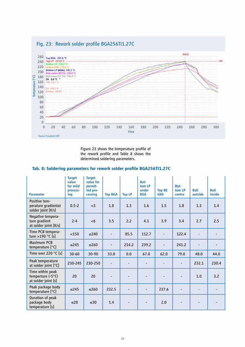
Figure 23 shows the temperature profile of the rework profile and Table 8 shows the determined soldering parameters.
Fig. 23: Rework solder profile BGA256TI1.27C
Source: Fraunhofer ISIT
Parameter
Target value for mild process-ing
Target value for permit-ted pro-cessing TopBGA Top LP
Bot-tom LP under BGA
Top BE G80
Bot-tom LP centre
Ball outside
Ball inside
Positive tem-perature gradientat solder joint [K/s]
0.5-2 <3 1.8 1.3 1.6 1.5 1.8 1.3 1.4
Negative tempera-ture gradient at solder joint [K/s]
2-4 <6 3.5 2.2 4.1 3.9 3.4 2.7 2.5
Time PCB tempera-ture >190 °C [s] <150 ≤240 - 85.5 112.7 - 122.4 - -
Maximum PCB temperature [°C] ≤245 ≤260 - 214.2 239.2 - 241.2 - -
Time over 220 °C [s] 30-60 30-90 33.0 0.0 67.0 62.0 79.0 48.0 44.0
Peak temperature at solder joint [°C] 230-245 230-250 - - - - - 232.1 230.4
Time within peak temperture (-5°C) at solder joint [s]
20 20 - - - - - 1.0 3.2
Peak package body temperature [°C] ≤245 ≤260 232.5 - - 237.6 - - -
Duration of peak package body temperature [s]
≤20 ≤30 1.4 - - 2.0 - - -
Tab.8:SolderingparametersforreworksolderprofileBGA256TI1.27C
0 20 40 60 80 100 120 140 160 180 200 220 240 260 280 300
260240220200180160140120100806040200
Time
Tem
pera
ture
{°C
}
33
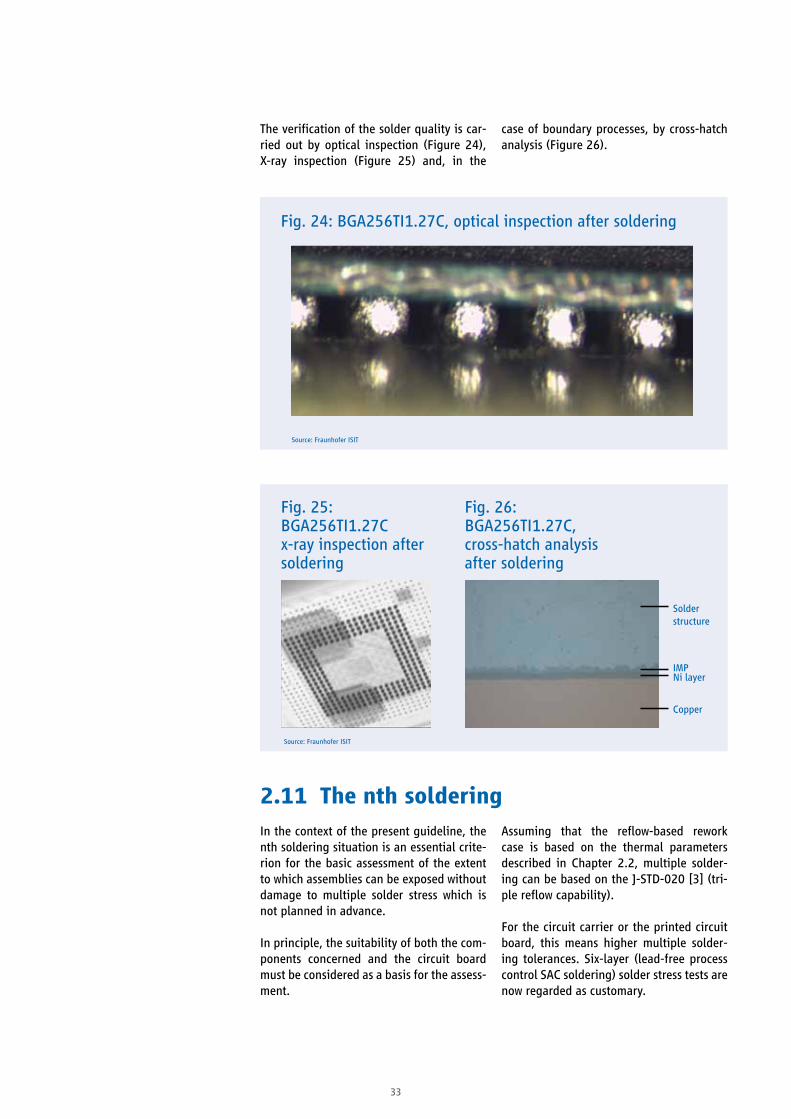
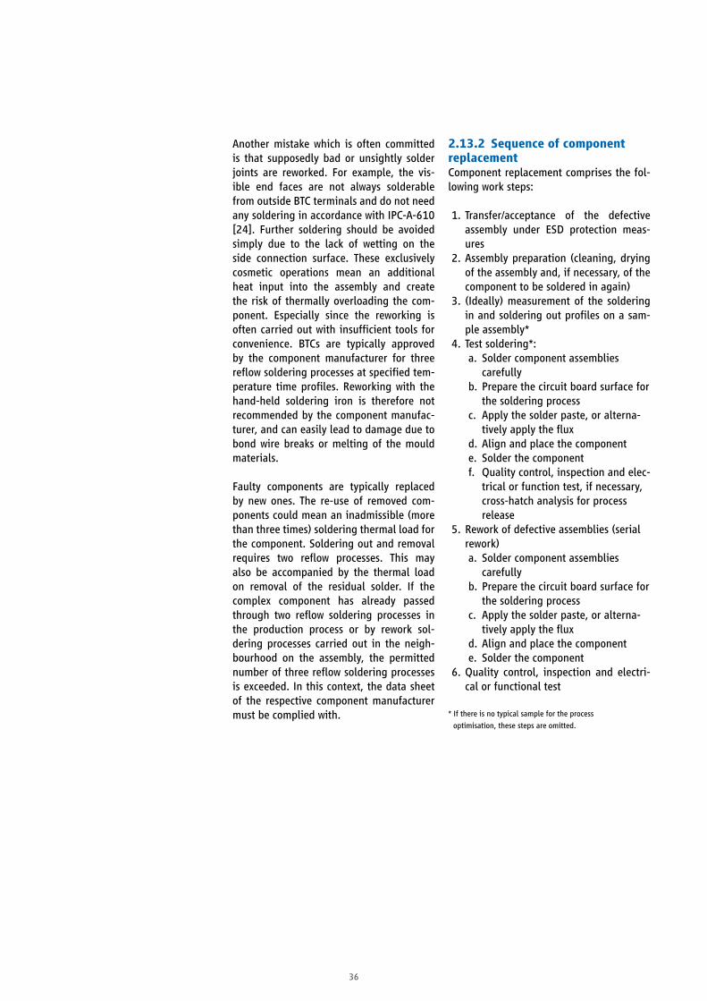
The verification of the solder quality is car-ried out by optical inspection (Figure 24), X-ray inspection (Figure 25) and, in the
case of boundary processes, by cross-hatch analysis (Figure 26).
In the context of the present guideline, the nth soldering situation is an essential crite-rion for the basic assessment of the extent to which assemblies can be exposed without damage to multiple solder stress which is not planned in advance.
In principle, the suitability of both the com-ponents concerned and the circuit board must be considered as a basis for the assess-ment.
Assuming that the reflow-based rework case is based on the thermal parameters described in Chapter 2.2, multiple solder-ing can be based on the J-STD-020 [3] (tri-ple reflow capability).
For the circuit carrier or the printed circuit board, this means higher multiple solder-ing tolerances. Six-layer (lead-free process control SAC soldering) solder stress tests are now regarded as customary.
Fig. 24: BGA256TI1.27C, optical inspection after soldering
Source: Fraunhofer ISIT
Fig. 25: BGA256TI1.27C x-ray inspection after soldering
Fig. 26: BGA256TI1.27C, cross-hatch analysis after soldering
Source: Fraunhofer ISIT
Solder structure
Ni layer
Copper
IMP
2.11 The nth soldering

34
The direct comparison between the reflow line process (full convection) and a com-parative view using rework systems with the same cycle loading in chapter 4.5 provides further information on the degrading effect of multiple solder stress scenarios.
The maximum upper limit for the risk assessment is the three-times thermal reworking at a component position which is not based on the actual correction require-ment, but should only represent the worst-case scenario.
The primary types of the heat transfer forms are shown below. In the following context only the forms of heat input (convection and radiation) which are customary for the use of rework systems are further consid-ered.
The heat demand of the assembly depends on the substrate, the components and the solder paste requirements. The amount of heat required ΔQ for heating to the solder-ing temperature results from
ΔQ=VxρxcpxΔT
with: ΔQ required heat quantity, V volume, Ρ density, C
p heat capacity of the
entire assembly and ΔT difference between room temperature and soldering temperature.
As a rule, the assembly is not in thermal equilibrium in the soft soldering process. The heat input is differentiated between heat conduction, convection and heat radia-tion. In the case of heat transfer, the essen-tial process variables to be considered are:• Achievable heat transfer coefficient α
(heat transfer efficiency)• Controllable temperature difference
between the heat source and the assem-bly
• Heat requirement of the assembly/solder-ing point (heat capacity and thermal resistance)
2.12 Heat transfer
Fig. 27: Development of connection technology
Source: University of Rostock
IR radiation
Component Solder joint
convection condensation microwave

35
Typical heat transfer figures in the rework process:
2.13.1 When an element "must" - "can" - "must not" be reworkedReworking the component is only useful if the cause of the error is identified. In the first place, all other possible faults should be checked and excluded as far as possible. Pull-up, blocking capacitors or subsequent IC components are often responsible for functional faults in assemblies, but in the electrical test a different component is indi-cated as the cause of the fault. In particular, complex components, e.g. BGAs, LGAs, BTCs
with their concealed solder joints which cannot be visually inspected, are likely to be classified as being defective. Therefore, further measures should be taken only after a reliable diagnosis which has correctly identified the component to be repaired or at least highly likely to be faulty, in order to remedy component, assembly or soldering defects. According to J-STD-001 [8]/Class 3, faults and rework must be documented (these ought to be documented for classes 1 and 2).
The most common soldering processes in the rework process are reflow soldering by means of convection and infrared radiation.
For reflow soldering with forced convection, a tempered gas (standardly nitrogen as a protective gas) is blown onto the assem-bly at a suitable flow rate. Here, the heat transfer coefficient α essentially depends on the flow velocity of the gas, whereas the surface colour is of no importance. It should be noted that too much airflow can blow away components. However, this danger is minimised by means of sensible parameter selection. With covers (hoods, solder masks) on the assembly, temperature-sensitive components can be protected against over-heating.
Reflow soldering with infrared radiation transfers the heat from ceramic surface or quartz lasers. Here, the heat transfer is pri-marily dependent on the temperature dif-
ference of the (hot) radiators to the object to be heated. A precondition for an efficient transfer to components and substrates is a low-loss coupling (absorption) into the materials to be heated. Radiation heat can be localised with simple methods (shield-ing). In reworking, a protective gas is gen-erally not used in IR soldering. Due to the high temperature of the radiator, thermal overloading of the surfaces can occur in inadequately controlled processes. How-ever, this danger is minimised by means of sensible parameter selection.
Hot gas rework systems, IR rework systems and a combination of both are widely used in the reworking of assemblies, and if the mode of operation is right, there is hardly any danger of damage to components and printed circuit boards.
2.13 Processflows
Tab. 9: Heat transfer forms
Heat transfer mechanism
Typical numerical values for heattransferefficiency(α)
Radiation 20 to 60 (primarily dependent on radiator temperature)
Management 500 (with ideal contact)
Convection 5-80 (primarily dependent on the flow velocity)
Source:Temperature Measurement in Reflow, Max H. Poech, Fraunhofer Institute for Silicon Technology, ISIT-Seminar Temperature Measurement Technology, October 2013 [23]
36
Another mistake which is often committed is that supposedly bad or unsightly solder joints are reworked. For example, the vis-ible end faces are not always solderable from outside BTC terminals and do not need any soldering in accordance with IPC-A-610 [24]. Further soldering should be avoided simply due to the lack of wetting on the side connection surface. These exclusively cosmetic operations mean an additional heat input into the assembly and create the risk of thermally overloading the com-ponent. Especially since the reworking is often carried out with insufficient tools for convenience. BTCs are typically approved by the component manufacturer for three reflow soldering processes at specified tem-perature time profiles. Reworking with the hand-held soldering iron is therefore not recommended by the component manufac-turer, and can easily lead to damage due to bond wire breaks or melting of the mould materials.
Faulty components are typically replaced by new ones. The re-use of removed com-ponents could mean an inadmissible (more than three times) soldering thermal load for the component. Soldering out and removal requires two reflow processes. This may also be accompanied by the thermal load on removal of the residual solder. If the complex component has already passed through two reflow soldering processes in the production process or by rework sol-dering processes carried out in the neigh-bourhood on the assembly, the permitted number of three reflow soldering processes is exceeded. In this context, the data sheet of the respective component manufacturer must be complied with.
2.13.2 Sequence of component replacementComponent replacement comprises the fol-lowing work steps:
1. Transfer/acceptance of the defective assembly under ESD protection meas-ures
2. Assembly preparation (cleaning, drying of the assembly and, if necessary, of the component to be soldered in again)
3. (Ideally) measurement of the soldering in and soldering out profiles on a sam-ple assembly*
4. Test soldering*:a. Solder component assemblies
carefullyb. Prepare the circuit board surface for
the soldering processc. Apply the solder paste, or alterna-
tively apply the fluxd. Align and place the componente. Solder the componentf. Quality control, inspection and elec-
trical or function test, if necessary, cross-hatch analysis for process release
5. Rework of defective assemblies (serial rework)a. Solder component assemblies
carefullyb. Prepare the circuit board surface for
the soldering processc. Apply the solder paste, or alterna-
tively apply the fluxd. Align and place the componente. Solder the component
6. Quality control, inspection and electri-cal or functional test
* If there is no typical sample for the process
optimisation, these steps are omitted.
37
Assembly outside specification
Pseudo error or Cosmetic imperfections
Determine the fault location of
the reworking process approved by the part manu-
facturer
Calibration of soldering and removal profiles
If necessary, rework of further assemblies
Procedure as above
Test soldering
Quality control
Rework (soldering of faulty solder joints, for example bridges, open solder joints, solder quantity)
Select a suitable solder pro-file, solder the component, Prepare LP and solder in new component
Solder profile,Solder the component, Prepare LP and solder in new component
Packaging and shipping or assemblies in further process flow
Documentation and assembly without reworking in further processing sequences
Error Yes No
Component replacementnecessary
Test assembly available
Quality controlpassed
Transfer/acceptance of the defective assembly under ESD protection measures
Assembly preparation (cleaning, drying the assembly and, if necessary, the component to be soldered in again
Yes
Yes
Yes
Yes
No
No
No
No
Completed

38
2.13.3 Detailedprocessflow
1. Transfer/acceptance of the defective assembly under ESD protection measuresThe defective assemblies are accepted under suitable ESD protection measures from our own production, as a customer recourse or as a service order. They are then transferred to the clean ESD-protected rework environ-ment. All further work must be carried out under ESD protection conditions.
2. Assembly preparation (cleaning, drying of the assembly and, if necessary, of the componenttobesolderedinagain)If necessary, the assemblies are cleaned with suitable cleaning processes. Sub-sequently, the components are dried, if necessary, according to the manufac-turer's instructions. The assemblies are also dried with suitable parameter selec-tion. In this case, the recommendation is to dry with a plastic housing at 125 °C for 24 hours in the circulating oven, analo-gous to most moisture-sensitive IC compo-nents. However, this can lead to damage in temperature-sensitive components. There-fore, the maximum temperature of the unit drying must be adapted to the most heat-sensitive component type. This requires a study of the data sheets, especially if the drying temperature is to be as high as pos-sible for reasons of time. Common combi-nations when using temperature-sensitive components are drying in the circulating oven for 48 hours at 80 °C. or 60 hours at 70 °C. (DIN EN 61192-5 [10], literature reference). Drying should always be carried out when the assembly has been open for more than the open time of the moisture-sensitive component (MSL class 3 e.g. 168 hours = 7 days).
3. Calibration of the soldering in and sol-deringoutprofilesonasampleassemblySince the proper solder profile setting is rarely achieved in the first run-up, the sol-der profile should be measured on a sample assembly as described above. The sample assembly is ideally an identical (defec-tive) assembly to be processed. This passes through several soldering processes and should no longer be put into circulation as a result of the additional thermal load. If a sample assembly is not available, at least the bare PCB is to be used. Although not equipped, it has a lower thermal mass, but
the profile finding can thus take place in a first approximation. If no sample assem-bly is available, proceed as described under Test Soldering.
4. Test solderinga. Solder component assemblies carefullyFor this purpose, the component is soldered with the previously meas-ured solder profile. If no solder pro-file can be measured, a temperature- time profile is set on the rework system which is expected to be able to solder the component. This setting is based on experi-ence gained with the same or similar assem-blies. In any case, a profile with mild initial parameters should be selected in order to be able to extend or increase the time and/or temperature in the peak phase during the soldering process. Experience with the rework system is helpful. Understanding how the rework system responds to differ-ent settings helps to minimise the number of necessary iterations. The approach of using a relatively low parameter setting to the soldering task has the advantage that it can be repeated in the event of an unsuccessful (too cool) soldering test. Set-ting the temperature too high (temperature or time) can lead to irreversible assembly damage. There is the possibility, according to IPC-7711/7721 [12], of repairing dam-aged printed circuit boards. However, this procedure is not recommended here.
An online control of the soldering process with a pivoting side camera is particularly helpful during the soldering process. This results in improved process reliability on rework on unknown assemblies. It is thus possible to observe the melting of the sol-der. It is only when the solder is completely melted that the component can be lifted safely without the need for individual, still solid solder connections to pad trimmers on circuit boards or components. If the com-ponent is lifted off, the soldering out pro-gramme is terminated or the cooling phase is initiated to cool the component and cir-cuit board.
b. Prepare the circuit board surface for the soldering process (residual solder removal, cleaning the pad surfaces)The circuit board is now freed of excess resid-ual solder and flux residues. This can be done manually or with machine support. In par-

39
ticular, BTCs are extremely sensitive to non- uniform soldering volumes of the individ-ual solder joints with regard to short-circuit formation, non-soldering and reliability. In this case, unlike in the case of BGAs, it is particularly important to ensure a uniform solder application (paste pressure) and to ensure a good uniform residual solder removal in advance. The "soldering" in the residual solder, as is often the case with BGAs with a larger grid size, is not recom-mended, since a uniform levelling of the residual solder amounts is only possible within specific limits. Therefore, the resid-ual solder should be reduced to a small residual quantity.
With the aid of a suitable flux, a safe, machine-supported residual solder removal which is mild on the printed circuit boards, is possible, for example by means of con-tactless vacuum extraction. However, care must also be taken to avoid the exposure of intermetallic phases by application of excessive temperatures or too long process times, since otherwise wetting problems may occur during the subsequent soldering process.
Improper use of manual soldering irons and/or de-soldering leads to the risk of damage or even tearing of printed circuit boards or adjacent components.
Pouring and varnish residues are removed according to IPC 7711/7721 [12].
If any impurities remain, they are removed with a suitable cleaning medium and a brush or lint-free cloth. Care must be taken to ensure that the cleaning medium is approved for this application and that no residues remain on the printed circuit board. In particular, no media should flow under adjacent components. If necessary, a subsequent automatic cleaning process will be necessary.
c. Application of solder paste (optionally on printed circuit board or component)In order to solder the new or cleaned old component, new solder paste must be applied. This is done by means of manual solder paste printing with so-called mini-sheets either on the printed circuit board or predominantly on the component bottom.
Rework device manufacturers offer option-ally available tools (see chapter 4.7).
The same pressure parameters (stencil thickness, opening size, layout) should be applied as in inline processing. If in doubt, work must be carried out according to the recommendation of the component manu-facturer or the stencil manufacturer.
Alternatively, manual (inaccurate dosing) or automatic dispensing or dipping transfer methods can also be used. It is important to use a uniform application of solder paste in order to achieve a good soldering result.
The solder application by manual soldering is unsuitable because of the difficult to con-trol process. A uniform pre-soldering as a basis for evenly shaped solder joints is very hard to make reliably reproducible. There is also the risk of component damage caused by the uncontrolled heat input. This method is not recommended for components that are only reflow-specified (many BTCs).
d. Align and place the componentThe component is recorded with the sup-port of the rework station, and aligned and placed with respect to the pin-1 mark. In particular, BTCs have only a limited abil-ity to float and thus compensate for a mis-alignment. Inaccurate positioning leads to bridging. In this case an offset of less than 25 percent of the connection width is rec-ommended according to IPC-7093 [7]. Typi-cally, alignment is by beam splitter and/or camera system. By comparing the images of pads or reference marks to the compo-nent, manual or automatic positioning (x, y, Θ) is possible. The component is then placed on the assembly.
e. Solder the componentThe component is soldered with a suitable rework station using the soldered profile which was measured or formed during des-oldering.
The soldering of, for example, a BTC with a soldering iron due to the inaccessible con-nection surfaces and the above mentioned dangers of damage caused by the uncon-trolled heat input is not recommended and is generally not compliant with the manu-facturer.

40
f. Process controlSuccess monitoring can be performed by optical inspection, X-ray inspection, and also by an electrical test or a functional test. In the case of boundary soldering (very low or very high heat input), a cross-hatch anal-ysis is recommended for process release. The solder joint is assessed for the wetting and formation of the intermetallic phase. In addition, the circuit board and components are examined for structural integrity.
5. Rework of defective assemblies (serial rework)After the test soldering and the process qualification has been completed, the series rework can be carried out. The speci-fications according to J-STD-020 [3] and J-STD-033 [4] must be complied with.
a. Solder component assemblies care-fully (see 4.a.)
b. Prepare the circuit board surface for the soldering process (see 4.b.)
c. Apply the solder paste or alterna-tively the flux (see 4.c.)
d. Align and place the component (see 4.d.)
e. Solder the component (see 4.e.)
6. Quality control, inspection and electri-cal or functional testThe quality control is carried out through non-destructive testing by means of opti-cal inspection (as far as possible) and x-ray inspection as well as the proof of electrical function.
2.14.1 Manual soldering devices1. Contact soldering (solderingiron,pliers,...)The classic soldering technique is the elec-tric soldering iron; although the patent of Ernst Sachs from the year 1921 is now only an historical document, the basic technol-ogy has proven itself to this day. The lead-ing manufacturers of hand tools focus on the refinement of heating and control tech-nology to adapt modern tools to the needs of electronics manufacturing. The solder-ing tips are becoming ever finer and the
demands on exact soldering tip tempera-tures ever higher. At the same time, today's highly integrated electronic assemblies often require a high amount of heat which requires intelligent post-heating behaviour, i.e. a rapid reaction of the heating system.
2.14 Device technology
Fig. 28: SMD soldering with contact heat (soldering tip)
Source: Ersa

41
Fig. 29: Heat flow in a soldering tip from the heating element to the active soldering surface, in the inner (green) sensor for detecting the temperature, heat flow in the two soldering tips of a pair of desoldering tweezers or in two soldering irons used in parallel.
Source: Ersa
Soldering iron manufacturers have long been focusing on the measurement of the real soldering tip temperature and thus ensure that the control always responds to the immediate change in this temperature.
This system has proven itself with solder-ing irons from all manufacturers. The cali-bration of the soldering tip temperature can also be carried out very simply by the user in a simple way and ensures that an accurate measurement and thermal control behavior is ensured at all times.
In addition to the proper temperature, it is the geometry of the soldering tip which often determines the success or failure of the soldering process.
The soldering tip must match the soldering task (Figure 30 and Figure 31).
The manufacturers have a wide range of sol-dering and desoldering tips for their solder-ing tools which is geared to the needs of the market and is constantly being expanded. The following pictures are showing exam-ples of mistakes that may occur when select-ing soldering tips, or the proper selection.
Fig. 30: Images of small soldering tips
Source: Fraunhofer ISIT

42
Fig. 32: Images of suitably wide, but too thick soldering tips
Source: Fraunhofer ISIT
Fig. 33: Images of correctly selected soldering tips
Source: Fraunhofer ISIT
Fig. 31: Images of too large soldering tips
Source: Fraunhofer ISIT

43
In addition, there are special soldering tips with which manufacturers can react to the needs of special applications.
There is an advantage in using soldering stations of which the soldering tips can also be changed during the heated state. This is particularly noticeable when the type and
size of the soldering tips must be influenced flexibly. Also the speed of the heating up and the temperature stability at the solder-ing tip do not play a negligible role in the process. The display standardly provides information on the temperature situation at the soldering tip.
Fig. 34: Exemplary coating of a soldering tip
Source: Ersa
Fig. 35: Soldering stations with directly heated soldering tips possible as single or double station
Source: Weller, JBC, Ersa
Nickelcoating
Nickel coating
The base material made of highly heat-conductive electrolyte copper ensures optimum heat transfer from the heating element to the coating
Iron coating
Chrome coating Corrosion and acceptance of the solder at undesired points
Schematic representation, not to scale
Coating on the soldering lane, de-pending on the tip type, up to 600 μm thick, wetting in the factory with lead-free solder
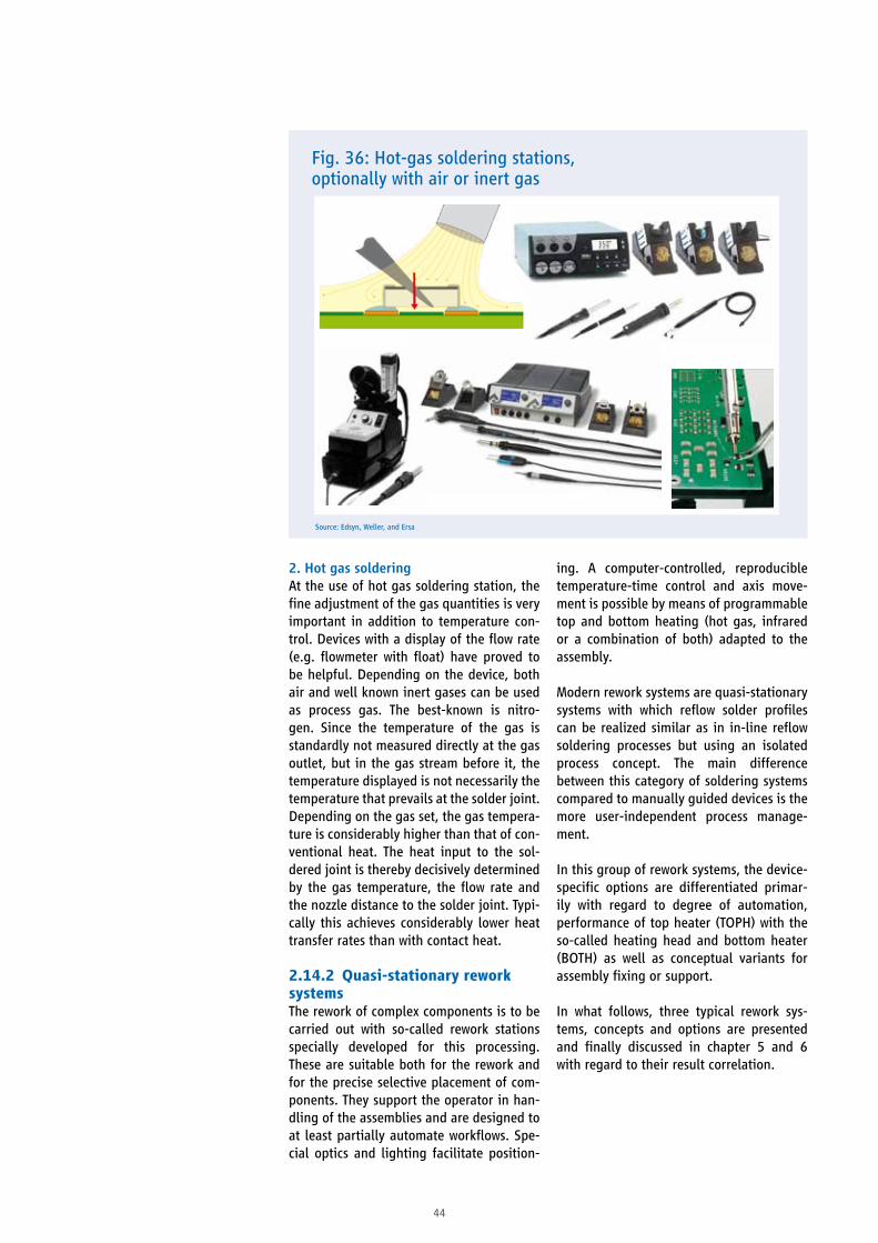
44
2. Hot gas solderingAt the use of hot gas soldering station, the fine adjustment of the gas quantities is very important in addition to temperature con-trol. Devices with a display of the flow rate (e.g. flowmeter with float) have proved to be helpful. Depending on the device, both air and well known inert gases can be used as process gas. The best-known is nitro-gen. Since the temperature of the gas is standardly not measured directly at the gas outlet, but in the gas stream before it, the temperature displayed is not necessarily the temperature that prevails at the solder joint. Depending on the gas set, the gas tempera-ture is considerably higher than that of con-ventional heat. The heat input to the sol-dered joint is thereby decisively determined by the gas temperature, the flow rate and the nozzle distance to the solder joint. Typi-cally this achieves considerably lower heat transfer rates than with contact heat.
2.14.2 Quasi-stationaryreworksystemsThe rework of complex components is to be carried out with so-called rework stations specially developed for this processing. These are suitable both for the rework and for the precise selective placement of com-ponents. They support the operator in han-dling of the assemblies and are designed to at least partially automate workflows. Spe-cial optics and lighting facilitate position-
ing. A computer-controlled, reproducible temperature-time control and axis move-ment is possible by means of programmable top and bottom heating (hot gas, infrared or a combination of both) adapted to the assembly.
Modern rework systems are quasi-stationary systems with which reflow solder profiles can be realized similar as in in-line reflow soldering processes but using an isolated process concept. The main difference between this category of soldering systems compared to manually guided devices is the more user-independent process manage-ment.
In this group of rework systems, the device-specific options are differentiated primar-ily with regard to degree of automation, performance of top heater (TOPH) with the so-called heating head and bottom heater (BOTH) as well as conceptual variants for assembly fixing or support.
In what follows, three typical rework sys-tems, concepts and options are presented and finally discussed in chapter 5 and 6 with regard to their result correlation.
Fig. 36: Hot-gas soldering stations, optionally with air or inert gas
Source: Edsyn, Weller, and Ersa

45
2.15.1 Semi-automatic Hot gas rework system
Fig. 37: Schematic image of rework station
Source: Airbus DS Electronics and Border Security
2.15 Devices - Systems - Concepts
Fig. 38: Semi-automatic hot gas rework system
Source: Martin
1. Placement arm (AVP) with LED ring light and HDD camera
2. Control unit3. 3000-W hybrid under-heating4. Hot air top heating5. Infrared temperature sensor
6. Nozzle for Dip, Print and μSMD Tool (APP TOOL)
7. Hand rest with cooling fan8. Stylus stand with: Dosing, soldering
and vacuum grippers9. Flexible circuit board support
(Flex Support)10. Side camera
1. Component (e.g., BGA)2. PCA 3. APCA Main Support4. Centre support5. Control optics 6. Component vacuum tool
7. Optical placement aid 8. Bottom heater (BOTH)9. Top heater (TOPH) 10. Process gas supply11. Temperature sensor 12. Control/Unit
5
1
2
6
4
3
9
10
7
8
1 2 3
4
5
7
9
6
10
12
11
BOTHBOTHBOTH8
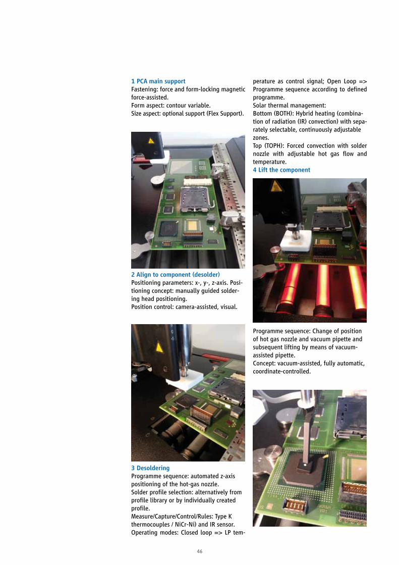
46
1 PCA main supportFastening: force and form-locking magnetic force-assisted.Form aspect: contour variable. Size aspect: optional support (Flex Support).
2Aligntocomponent(desolder)Positioning parameters: x-, y-, z-axis. Posi-tioning concept: manually guided solder-ing head positioning. Position control: camera-assisted, visual.
3 DesolderingProgramme sequence: automated z-axis positioning of the hot-gas nozzle.Solder profile selection: alternatively from profile library or by individually created profile. Measure/Capture/Control/Rules: Type K thermocouples / NiCr-Ni) and IR sensor. Operating modes: Closed loop => LP tem-
perature as control signal; Open Loop => Programme sequence according to defined programme. Solar thermal management: Bottom (BOTH): Hybrid heating (combina-tion of radiation (IR) convection) with sepa-rately selectable, continuously adjustable zones. Top (TOPH): Forced convection with solder nozzle with adjustable hot gas flow and temperature.4 Lift the component
Programme sequence: Change of position of hot gas nozzle and vacuum pipette and subsequent lifting by means of vacuum-assisted pipette. Concept: vacuum-assisted, fully automatic, coordinate-controlled.
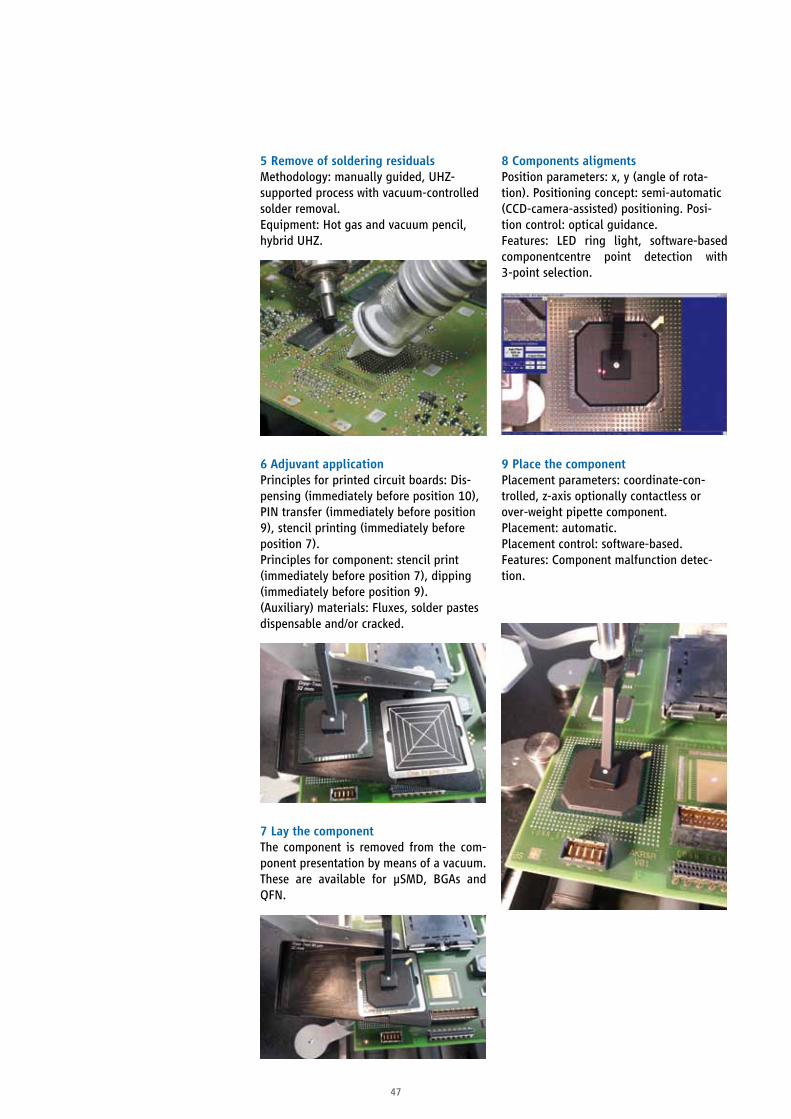
47
5 Remove of soldering residualsMethodology: manually guided, UHZ-supported process with vacuum-controlled solder removal. Equipment: Hot gas and vacuum pencil, hybrid UHZ.
6 Adjuvant applicationPrinciples for printed circuit boards: Dis- pensing (immediately before position 10), PIN transfer (immediately before position 9), stencil printing (immediately before position 7).Principles for component: stencil print (immediately before position 7), dipping (immediately before position 9). (Auxiliary) materials: Fluxes, solder pastes dispensable and/or cracked.
7 Lay the componentThe component is removed from the com-ponent presentation by means of a vacuum. These are available for μSMD, BGAs and QFN.
8 Components aligmentsPosition parameters: x, y (angle of rota-tion). Positioning concept: semi-automatic (CCD-camera-assisted) positioning. Posi-tion control: optical guidance. Features: LED ring light, software-based componentcentre point detection with 3-point selection.
9 Place the componentPlacement parameters: coordinate-con-trolled, z-axis optionally contactless or over-weight pipette component. Placement: automatic. Placement control: software-based. Features: Component malfunction detec-tion.
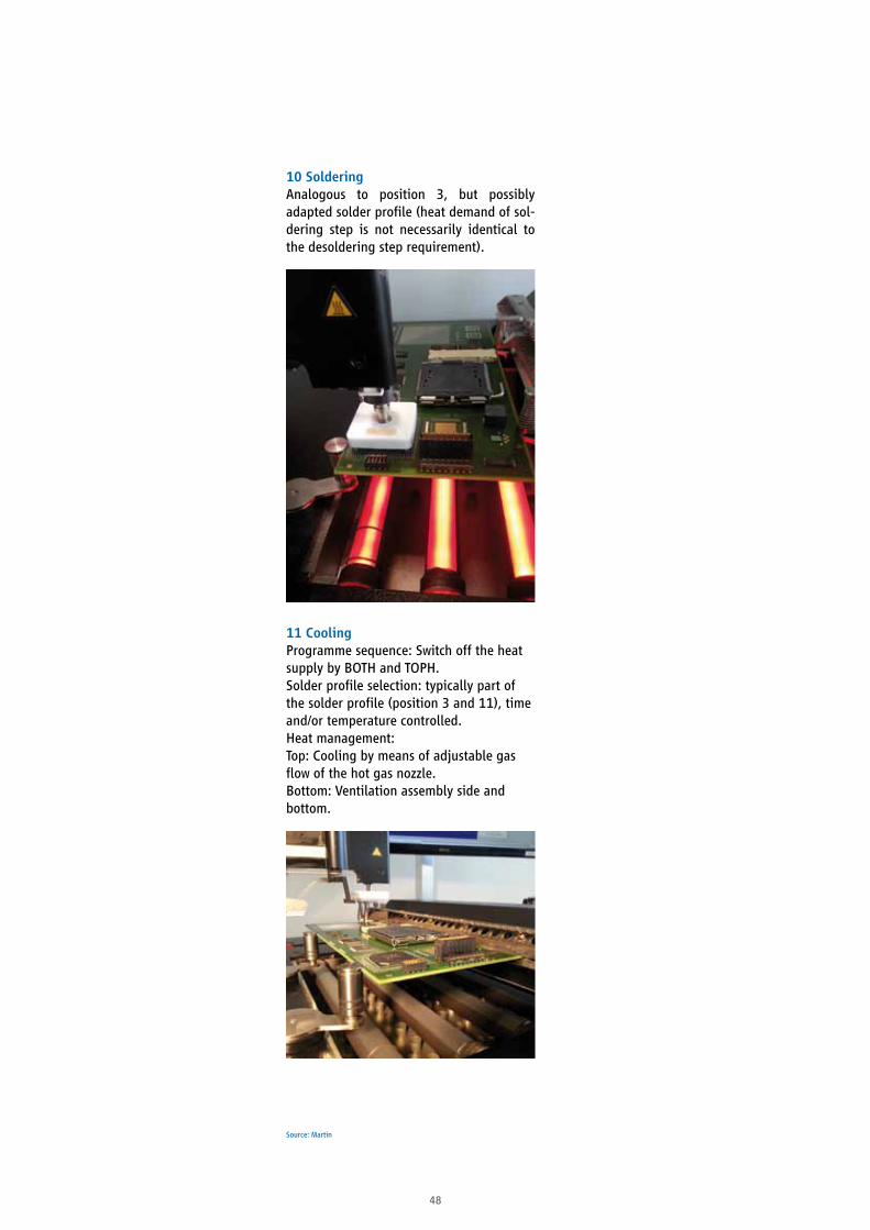
48
10 SolderingAnalogous to position 3, but possibly adapted solder profile (heat demand of sol-dering step is not necessarily identical to the desoldering step requirement).
11 CoolingProgramme sequence: Switch off the heat supply by BOTH and TOPH. Solder profile selection: typically part of the solder profile (position 3 and 11), time and/or temperature controlled. Heat management: Top: Cooling by means of adjustable gas flow of the hot gas nozzle. Bottom: Ventilation assembly side and bottom.
Source: Martin
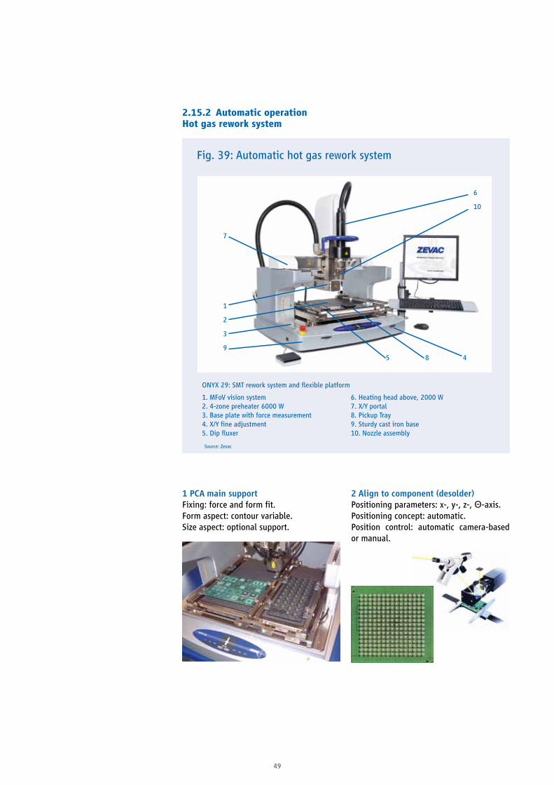
49
2Aligntocomponent(desolder)Positioning parameters: x-, y-, z-, Θ-axis. Positioning concept: automatic. Position control: automatic camera-based or manual.
1 PCA main supportFixing: force and form fit.Form aspect: contour variable. Size aspect: optional support.
2.15.2 Automatic operation Hot gas rework system
Fig. 39: Automatic hot gas rework system
Source: Zevac
1. MFoV vision system2. 4-zone preheater 6000 W3. Base plate with force measurement4. X/Y fine adjustment5. Dip fluxer
6. Heating head above, 2000 W7. X/Y portal8. Pickup Tray9. Sturdy cast iron base10. Nozzle assembly
ONYX 29: SMT rework system and flexible platform
1
2
3
95 8 4
6
10
7
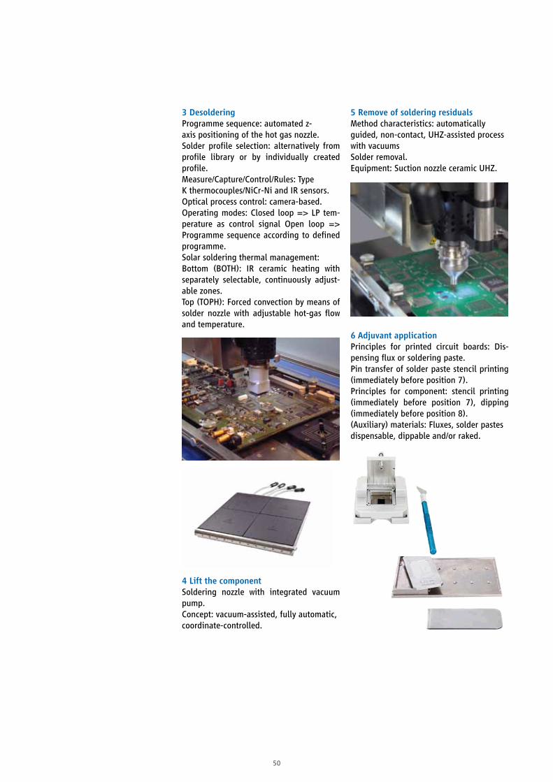
50
5 Remove of soldering residualsMethod characteristics: automatically guided, non-contact, UHZ-assisted process with vacuums Solder removal.Equipment: Suction nozzle ceramic UHZ.
6 Adjuvant applicationPrinciples for printed circuit boards: Dis-pensing flux or soldering paste.Pin transfer of solder paste stencil printing (immediately before position 7). Principles for component: stencil printing (immediately before position 7), dipping (immediately before position 8). (Auxiliary) materials: Fluxes, solder pastes dispensable, dippable and/or raked.
3 DesolderingProgramme sequence: automated z- axis positioning of the hot gas nozzle. Solder profile selection: alternatively from profile library or by individually created profile.Measure/Capture/Control/Rules: Type K thermocouples/NiCr-Ni and IR sensors.Optical process control: camera-based. Operating modes: Closed loop => LP tem-perature as control signal Open loop => Programme sequence according to defined programme.Solar soldering thermal management: Bottom (BOTH): IR ceramic heating with separately selectable, continuously adjust-able zones.Top (TOPH): Forced convection by means of solder nozzle with adjustable hot-gas flow and temperature.
4 Lift the componentSoldering nozzle with integrated vacuum pump.Concept: vacuum-assisted, fully automatic, coordinate-controlled.

51
7 Lift the componentThe component is removed automatically from pinpoint 1 with freely oriented record-ing positions.
8 Lift the alignment of componentPosition parameters: x, y (angle of rota-tion). Positioning concept: fully automatic, camera-assisted positioning. Position control: Pin overlay.Features: Creation of an overlay of printed circuit board and component by prism.
9 Lift the alignment of componentPlacement parameters: coordinate- controlled, z-axis optionally with defined force or contactless. Placement: automatic. Placement control: with camera support. Features: manual misalignment, correction.
10 SolderingAnalogous to position 3, but possibly adapted solder profile (heat demand of soldering step is not necessarily identical to the desoldering step requirement).
11 CoolingProgramme sequence: Switch off the heat supply by BOTH and TOPH.Solder profile selection: typically part of the solder profile (position 3 and 10), time and/or temperature controlled. Heat management: Top: Cooling by means of adjustable gas flow of the hot gas nozzle.Bottom: air-cooled surface cooling via cold air knife.
Source: Zevac
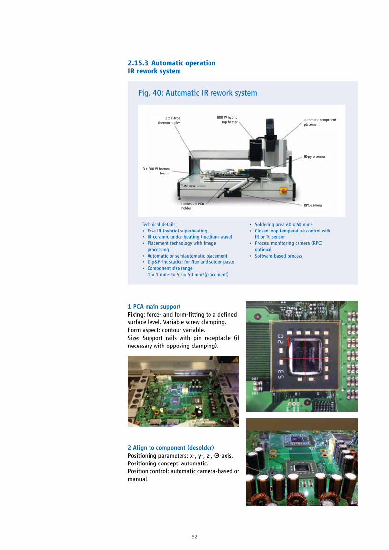
52
2.15.3 Automatic operation IR rework system
Fig. 40: Automatic IR rework system
Technical details:• Ersa IR (hybrid) superheating• IR-ceramic under-heating (medium-wave)• Placement technology with image
processing• Automatic or semiautomatic placement• Dip&Print station for flux and solder paste• Component size range
1 × 1 mm² to 50 × 50 mm²(placement)
• Soldering area 60 x 60 mm²• Closed loop temperature control with
IR or TC sensor• Process monitoring camera (RPC)
optional• Software-based process
1 PCA main supportFixing: force- and form-fitting to a defined surface level. Variable screw clamping. Form aspect: contour variable. Size: Support rails with pin receptacle (if necessary with opposing clamping).
2Aligntocomponent(desolder)Positioning parameters: x-, y-, z-, Θ-axis. Positioning concept: automatic. Position control: automatic camera-based or manual.
2 x K-type thermocouples
800 W hybrid top heater
automatic component placement
IR-pyro sensor
RPC-camera removable PCB holder
3 x 800 W bottom heater

53
5 Remove of soldering residuesProcess characteristics: manually guided, BOTH-supported process with external con-tact heat or vacuum suction.
6 Adjuvant applicationPrinciples for printed circuit boards: flat flux application (e.g. brush application) is not recommended Principles for component: Stencil printing (immediately before position 7), dipping (immediately before position 9). (Auxiliary) materials: Fluxes, solder pastes dispensable, dippable and/or raked.
3 DesolderingProgramme sequence: automated z-axis positioning of the IR hybrid heating head. Selecting a solder profile: either from pro-file library or by using a custom profile, as desired. Measure/Capture/Control/Rules: Type K thermocouples / NiCr-Ni and IR sensors. Optical process control: camera-based. Operating modes: Closed loop => LP tem-perature as control signal Open loop => Programme sequence according to defined programme. Soldering thermal management: Under-heating (BOTH): medium-wave infra-red. IR ceramic heating with separately selectable, continuously adjustable zones. Top (TOPH): IR hybrid heating head. IR ceramic heating with separately selecta-ble, continuously adjustable zones.
4 Lift the componentProgramme sequence: vacuum pipette inte-grated in the hybrid heating head. Concept: vacuum-assisted, fully automatic, coordinate-controlled.

54
9 Place the componentPlacement parameters: coordinate-con-trolled, z-axis optionally with defined force or contactless. Placement: automatic. Placement control: camera-supported. Features: manual misalignment.
7 Lay the componentThe component is provided with proper ori-entation of pin 1 on the glass plate of the camera system and automatically picked up.
8 Align the componentPosition parameters: x, y (angle of rota-tion). Positioning concept: fully automatic, camera-assisted positioning. Position control: Pin overlay. Features: automatic component recogni-tion. Creation of an overlay of printed cir-cuit board and component by prism.
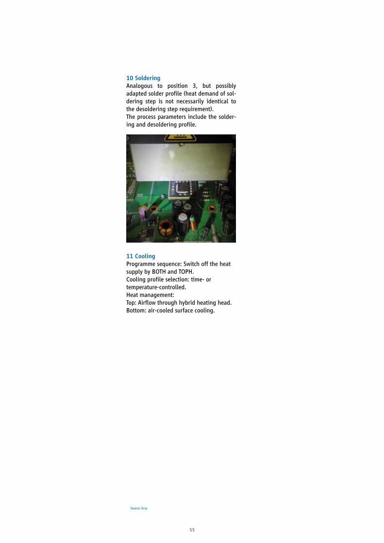
55
10 SolderingAnalogous to position 3, but possibly adapted solder profile (heat demand of sol-dering step is not necessarily identical to the desoldering step requirement).The process parameters include the solder-ing and desoldering profile.
11 CoolingProgramme sequence: Switch off the heat supply by BOTH and TOPH.Cooling profile selection: time- or temperature-controlled. Heat management:Top: Airflow through hybrid heating head.Bottom: air-cooled surface cooling.
Source: Ersa
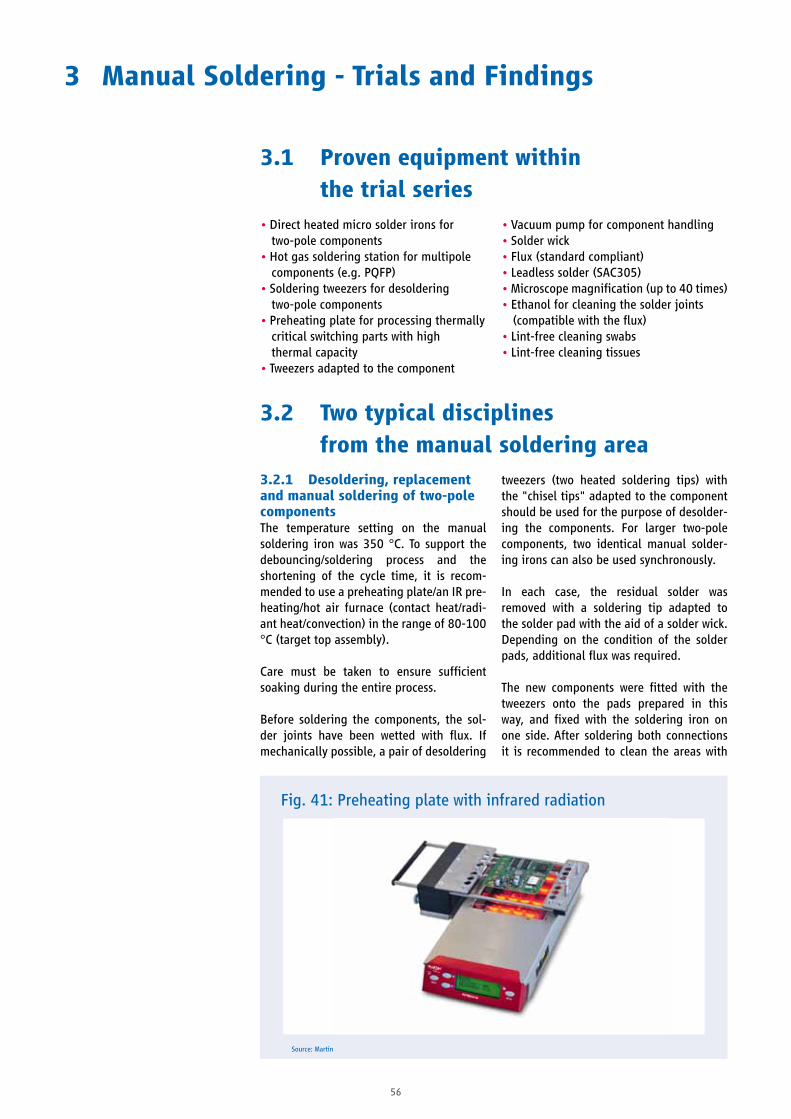
56
3.2 Two typical disciplines from the manual soldering area
3 Manual Soldering - Trials and Findings
• Direct heated micro solder irons for two-pole components
• Hot gas soldering station for multipole components (e.g. PQFP)
• Soldering tweezers for desoldering two-pole components
• Preheating plate for processing thermally critical switching parts with high thermal capacity
• Tweezers adapted to the component
• Vacuum pump for component handling• Solder wick• Flux (standard compliant)• Leadless solder (SAC305)• Microscope magnification (up to 40 times)• Ethanol for cleaning the solder joints
(compatible with the flux)• Lint-free cleaning swabs• Lint-free cleaning tissues
3.2.1 Desoldering, replacement and manual soldering of two-pole componentsThe temperature setting on the manual soldering iron was 350 °C. To support the debouncing/soldering process and the shortening of the cycle time, it is recom-mended to use a preheating plate/an IR pre-heating/hot air furnace (contact heat/radi-ant heat/convection) in the range of 80-100 °C (target top assembly).
Care must be taken to ensure sufficient soaking during the entire process.
Before soldering the components, the sol-der joints have been wetted with flux. If mechanically possible, a pair of desoldering
tweezers (two heated soldering tips) with the "chisel tips" adapted to the component should be used for the purpose of desolder-ing the components. For larger two-pole components, two identical manual solder-ing irons can also be used synchronously.
In each case, the residual solder was removed with a soldering tip adapted to the solder pad with the aid of a solder wick. Depending on the condition of the solder pads, additional flux was required.
The new components were fitted with the tweezers onto the pads prepared in this way, and fixed with the soldering iron on one side. After soldering both connections it is recommended to clean the areas with
3.1 Proven equipment within the trial series
Fig. 41: Preheating plate with infrared radiation
Source: Martin

57
3.3 Findings on manual soldering
a suitable cleaning medium and lint-free cleaning cloths, if a machine cleaning pro-cess does not follow. If the requirements from the point of view of the climate load demand, a "flux test" is mandatory. This ensures that corrosive residues are removed.
3.2.2 ProcessingofPQFPcomponentsWhen the components are removed, the sol-der joints are first wetted with flux.
The preheating of the component and the soldering points by means of the hot gas nozzle causes activation of the flux. There-after, the soldering points are heated to the melting point with the nozzle provided for the assembly. The time of remelting must be optically controlled by the operator. If all the soldering points are in the molten state, the component can be lifted off the assembly by means of a suitable tool (in this case with a vacuum pump). The residual solder is removed by means of desoldering. Ethanol is used as cleaning medium for flux residues.
The PQFP is first placed, optically manually aligned and tacked diagonally to the solder-ing iron at two terminals. The connections are wetted with flux and soldered with a depot soldering tip.
If solder bridges are formed, they are removed again with additional flux and a previously cleaned depot tip.
Following the soldering process, thorough manual cleaning is carried out.
Fig. 42: Combined stations with directly heated soldering iron and desoldering tweezers for two-pole components
Source: Weller, JBC
Soldering temperature/Soldering tip tem-peratureFor SAC solders a temperature range between 320 °C and 370 °C can be rec-ommended. The temperature is, of course, decisively determined by the thermal capac-ity of the components and the mass ratios in the immediate vicinity of the soldering point to be processed.
PreheatingAs a guideline, the temperature of >130 °C should not be exceeded on the underside of the assembly. This temperature is also dependent on the flow, since the efficacy of some fluxes, depending on time and tem-perature, is greatly reduced.

58
At the preheat temperature, the guidelines for occupational health and safety must be complied with. This can be done, for exam-ple, by marking or covering the hot sur-faces. It is in any case sensible to inform the competent safety specialist (internally/externally) in advance.
Soldering in/out of high-poles SMD (e.g. PQFP,TSSOP,...)Manual soldering was not recommended during the course of the studies. During the soldering process, pad damage or tear-ing can occur if, at the time of lifting, not all soldering points are molten. In the case of soldering in, terminal pins can be bent and due to the assembly density an ideal soldering iron guide cannot always be guar-anteed. It is strongly recommended to use a rework station suitable for this purpose.
Remove componentVacuum pipettes and gripping systems (tweezers, etc.) have proven themselves for the lifting of components.
Removal of residual solderWhen using solder wicks, a suitable dimen-sioning of the soldering tip must be ensured according to the width of the solder wick. Preheating the assembly to 60-100 °C and using a relatively wide soldering tip reduces the risk of pad damage and tear. The amount of heat required to be supplied via the desoldering wire is reduced by the preheating and the probability of unwanted solidification of the solder with the desol-dering wire is reduced.
The use of flux gel has the advantage of bet-ter heat transfer and supports the glide of the solder wick.
CleaningBoth the cleaning medium and the clean-ing process must be selected to match the flux residues and the compatibility with the assembly. An automatic assembly cleaning is recommended due to the reproducibility and safe removal of the dissolved residues.
Suitable designs for solderingRegarding solderable structures, it is impor-tant to consider two aspects:• Is the manual soldering process in prin-
ciple capable of producing acceptable soldering joints within predetermined thermal, temporal limits (heat resistance, maximum temperature specifications of the component manufacturer, etc.)?
• Is the manual soldering process due to the heat transfer form by means of con-duction (heat conduction) in principle approved for the design to be machined?
In Fig. 43, the component positions of the test board examined in detail are marked with soldering photograms. The reflow sym-bol is the indicator for a preferably reflowable construction and this circum-stance is frequently associated with a non-solderable design. The hand solder symbol indicates a component that is hand solderable. While these application restrictions apply to the soldering, it is also possible that component patches are not released for reflow soldering. As a result, reworking is not permitted using rework system.
Soldering fume extraction Industrial soldering stations with interface are available which can control a solder fume extraction for cleaning the process air. The interface ensures that the extraction is only
Fig. 43: Overview of the soldered or reflow soldered design of the testboard
Source: Zollner
59
carried out when soldering is performed. This saves energy and filter costs. A selec-tion of suction arms and nozzles ensures the optimal extraction of the soldering dust in every application. It should also be borne in mind that these suction stations must be subject to regular functional checks in accordance with the applicable regulations.
In order to protect the employees, a fume extractor must be used in the workplace. This compulsory use is specified by the respective EU safety data sheet of the sub-stance used.
Considered regulations on the topic of sol-der fumes extraction and regular testing:• GefStoffV Hazardous Substances Ordi-
nance [26] (Annex II, Chapter 2.3, Para-graph 7)
• TRGS 420 [27] "Process and material-spe-cific criteria for hazard assessment" refers to BGI 790-014 [28] "Soldering with the soldering iron" in clause 5.1 paragraph 3
• TRGS 406 [29] "Sensitising substances for the respiratory tract", pt. 5. Fig. 2:
• TRGS 900 [30] "Workplace limit values"• TRGS 528 [31]

60
The extent to which the determined solder profiles meet the targets of an assembly compatible soldering process is shown here. Table 10 (Target-to-actual adjustment of the profile parameters for rework processes) shows the comparison of the target specifi-cations with the determined profile param-eters.
The determined solder profiles correspond to the real application and were made under the requirement to ensure the com-plete melting of the solder connections. If there is only one assembly to be reworked no optimal solder profile adjustment is pos-sible. The user will select a set of param-eters which ensures the simultaneous melt-ing of all soldering joints which can result in slightly higher temperatures and longer times above liquidus temperature than the values defined in chapter 2.2 as a pre-set for an assembly-compatible soldering pro-cess.
Some of the values for the positive tem-perature gradient are below 1.0 K/s. This is dependent on the thermal mass of the assembly as well as on the heating power used. However, under the specification of a carefully soldering process, very low tem-perature gradients of up to 0.5 K/s are pos-sible, as long as all other specifications are adhered to (in particular maximum times over defined temperatures and the require-ments of the flux producer).
If the component to be soldered has a large thermal mass, the values for the negative temperature gradient are partially exceeded. It is important here not to pro-long the times above liquidus temperature so as to limit the growth of the intermetallic phase. If necessary, additional cooling must be used.
The requirements of the printed circuit board with respect to their thermal load were all respected.
The requirement to extend the time above liquidus temperature not over 60 seconds is only partially respected. If the achieved time is below 90 seconds, this is also con-sidered uncritical.
The specified peak temperature in the sol-der joint is not exceeded and the maximum time in the peak is maintained.
The maximum permitted value for the component surface temperature was not exceeded, in addition the manufacturing specifications have been complied. The maximum time for the peak temperature was maintained.
In summary, it can be said that the deter-mined and applied soldering profiles meet the requirements for a carefully rework pro-cess across different rework systems.
In chapter 4.5, the effect of the thermal load in the rework process with the profiles determined here is investigated.
For example, the soldering profiles of the rework systems used for the BGA256TI1.27C are shown below, see figures 44, 45 and 46.
4 Findings from the R+R Studies
4.1 Thermalprofiles(target-actual)
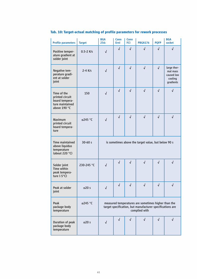
61
Profileparameters TargetBGA256:
Conn Erni
Conn FCI PBGA176 PQFP
BGAsocket
Positive temper-ature gradient at solder joint
0.5-2 K/s √√ √ √ √ √
Negative tem-perature gradi-ent at solder joint
2-4 K/s √√ √ √ √ large ther-
mal mass caused low
cooling gradients
Time of the printed circuit board tempera-ture maintained above 190 °C
150 √√ √ √ √ √
Maximum printed circuit board tempera-ture
≤245 °C √√ √ √ √ √
Time maintained above liquidus temperature (about 220 °C)
30-60 s is sometimes above the target value, but below 90 s
Solder joint Time within peak tempera-ture (-5°C)
230-245 °C √√ √ √ √ √
Peak at solder joint
≤20 s √√ √ √ √ √
Peak package body temperature
≤245 °C measured temperatures are sometimes higher than the target specification, but manufacturer specifications are
complied with
Duration of peak package body temperature
≤20 s √√ √ √ √ √
Tab.10:Target-actualmatchingofprofileparametersforreworkprocesses
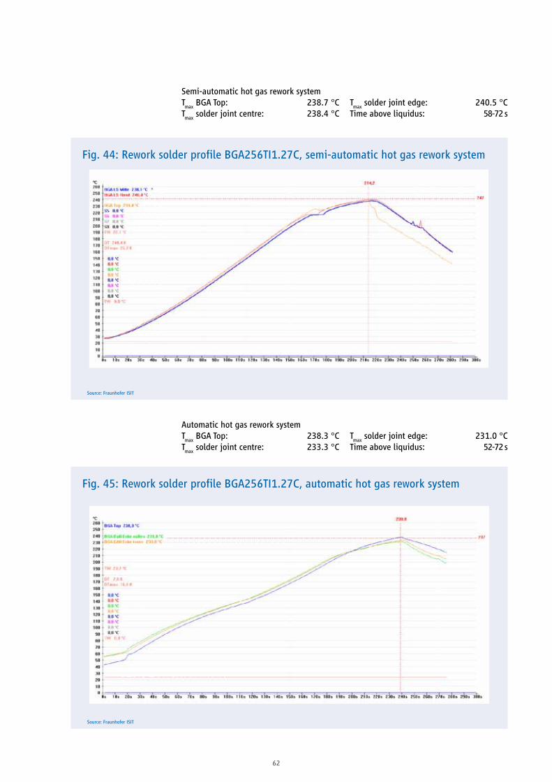
62
Fig. 44: Rework solder profile BGA256TI1.27C, semi-automatic hot gas rework system
Source: Fraunhofer ISIT
Fig. 45: Rework solder profile BGA256TI1.27C, automatic hot gas rework system
Source: Fraunhofer ISIT
Semi-automatic hot gas rework systemT
max BGA Top: 238.7 °C
Tmax
solder joint centre: 238.4 °CT
max solder joint edge: 240.5 °C
Time above liquidus: 58-72 s
Automatic hot gas rework systemT
max BGA Top: 238.3 °C
Tmax
solder joint centre: 233.3 °CT
max solder joint edge: 231.0 °C
Time above liquidus: 52-72 s

63
Tmax
BGA Top: 235.1 °CT
max solder joint centre: 238.0 °C
Tmax
solder joint edge: 240.7 °CTime above liquidus: 70-84 s
All investigated rework systems provide equivalent soldering profile characteristics which meet the requirements for soldering.
While, as a result of various rework or repair soldering processes, the functionality of the assembly can be decisively influenced or even impaired in its functionality, a clear assignment of effects, isolated for the printed circuit board texture, is often very difficult.
The printed circuit board occupies a special role as a dominant functional unit of a cir-cuit carrier and at the same time as a physi-cal foundation of the electronic assemblies.
Fig. 46: Rework solder profile BGA256TI1.27C, automatic IR rework system
Source: Fraunhofer ISIT
Parameter
Semi-Auto-matic hot gas rework system
Automatic hot gas rework system
Automatic IR rework system
Tmax
BGA Top [°C]: 238.7 238.3 235.1
Tmax
solder joint centre [°C]: 238.4 233.3 238.0
Tmax
solder joint edge [°C]: 240.5 231 240.7
Time above liquidus [sec]: 58-72 52-72 70-84
Tab. 11: Comparison of selected parameters for ReworksolderprofileBGA256TI1.27C
4.2 Printed circuit board as the dominant component
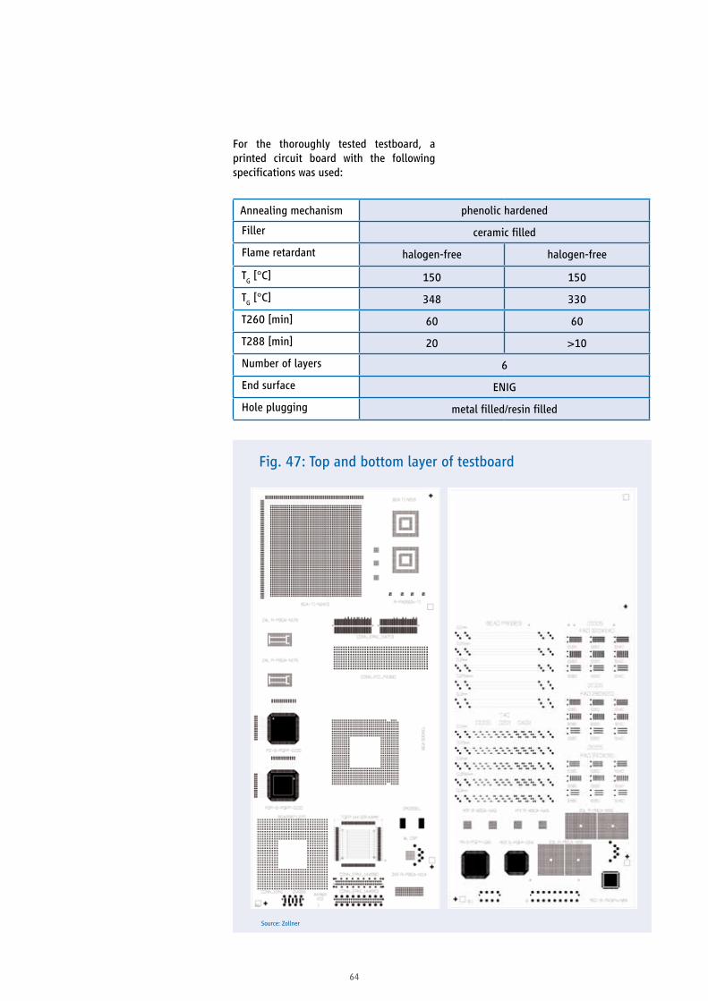
64
Fig. 47: Top and bottom layer of testboard
Source: Zollner
Annealing mechanism phenolic hardened
Filler ceramic filled
Flame retardant halogen-free halogen-free
TG [°C] 150 150
TG [°C] 348 330
T260 [min] 60 60
T288 [min] 20 >10
Number of layers 6
End surface ENIG
Hole plugging metal filled/resin filled
For the thoroughly tested testboard, a printed circuit board with the following specifications was used:

65
Fig. 48: Layer structure details
Source: Zollner
The underlying individual local rework pro-cess cumulatively represents the stress col-lective for the entire assembly and thus, in particular, also for the printed circuit board.
With respect to the diagnostic options for the assessment of the damage effects occur-ring, there are in principle two variants.
One variant is based on a non-destructive, visual inspection (e.g. on the basis of the acceptance requirements from IPC-A-610 [24]), while the second variant is based on a destructive test which is primarily intended to reveal the internal damage to the printed circuit board.
In the context of a visual examination under specific consideration of the post-processed areas, the following damage/effects can typically be expected:
• Lifted • Pads ripped of• Discolouration of solder resist• Discolouration of base material• Burning, charring• Changes to the circuit board surface• Measling• Delamination• Bow/Twist
In the context of a destructive examination under specific consideration of the post-processed areas, the following damage/effects can typically be expected:
• Barrel plating crack as well as attachment defects
• Deformation of plated through holes• Attachment defects in microvias • Delaminations
Summarizing Particularly at locations of the assembly, where took place a local (multiple) overlap of rework steps, it is necessary to subject the resulting thermal cutting quantities to a more detailed view since the potential of a PCB damage is the highest.
Depending on the frequency, intensity, concept and process management of the soldering processes used for the rework, there are more or less typical abnormali-ties or fault images on the printed circuit board which are shown in chapter 4, 5 in a configuration-specific manner.
Top Mask
copper foil
Prepreg
Prepreg
Prepreg
Prepreg
Prepreg
Prepreg
core
core
copper foil
copper foil
copper foil
copper foil
copper foil
Artwork_21Top Layer Artwork_1 18 μm finished copper thickness > 35 μm
Multi Layer 1 Artwork_2 35 μm
CORE 350 μm
CORE 350 μm
Multi Layer 3 Artwork_4 35 μm
Multi Layer 4 Artwork_5 35 μm
Bottom Layer Artwork_20 18 μm finished copper thickness > 35 μm
Bottom Mask Artwork_22
end thickness (overall): 1.6 mm
Multi Layer 2 Artwork_3 35 μm

66
4.3.1 Two-pole, passive ComponentsIn order to simulate the requirements of industrial components, a wide range of pas-sive components has been implemented in the layout.
The applied components range from 0402 (1.0 mm x 0.5 mm), via the 0201 design (0.6 mm x 0.3 mm), to 01005 with an edge length of 0.4 mm x 0.2 mm.
The challenge for the operator is to find a structured, prudent way of working with component rework in the array arrange-ment.
In particular, the replacement of compo-nents in this compact arrangement places the maximum demands on the tool as well as on the skill required.
Fig. 49: Thermal stress on the testboard
Source: Airbus DS Electronics and Border Security
4.3 Componentspecifications, ordered according to their complexity
Fig. 50: Array of passive components
Source: Zollner

67
4.3.2 Two-pole, passive ferrite inductor with high heat demandThe high heat demand of the ferrite core inductor must be taken into account in order to achieve successful rework. The pad area, and thus the connection to the printed circuit board, is minimised in relation to the component size and places high demands on the operator in order to avoid typical rework faults such as padlifting or pad loss.
4.3.3 ComponentswithflatGullwing connectorsCharacteristics of the classic Quad-Flat-Package-Forms (QFP):• Pitch 0.5 mm • Reduced mechanical strength of electri-
cally non-connected pads alternating with functional pads
• Thermal bridges connected to the inner layers in the corner areas
• Connection to central thermal pad con-nected via several layers
The classic design QFP is in principle easy to handle, but modern layouts and massive thermal pads complicate a successful rework.
4.3.4 SMT connectors in mixed SMT-THT technologyThe combination of SMT signal contacts and shielding using THT "pin-in-paste" technol-ogy confronts both production and rework-ing with new challenges.
4.3.5 Classic ball grid array designsIn order to qualify the industrial standard practiced rework process at a BGA, the Rework and Repair Working Group has developed strategies that make it possible to examine critical features of the rework:• Control pads, implemented as circumfer-
ential, soldered pads: →Which area is melted during the rework as an "undesired" effect?
• Various differences in the anchoring/attachment of the pads: →Check the thermal limits of the rework →How do maximum stresses affect mini-mal anchorages?
• Daisy chain structures across all balls of the BGA →Simple recognition of the success in the nth rework case
Fig. 51: Ferrite inductor in a thermally heterogeneous environment between CSP and BGA socket
Source: Zollner
Fig. 52: QFP components
Source: Zollner

68
To show the variety of requirements a modern rework process has to cover, there are components with fine pitch as well as an extremely high number of connec-tions and different edge lengths on the testboard.
Fig. 53: Connectors with SMT and THT connections
Source: Zollner
Fig. 54: Various BGA components with circumferential pads
Source: Zollner
Fig. 55: Size comparison of BGAs
Source: Zollner

69
4.3.6 Array connectors (BGApin-out)The connector is thermally sensitive and has precision gold contacts with leadfree balls.
Especially for the rework process, the place-ment aid has been modified to improve the effect of convection.
4.3.7 BGA socketThe BGA socket consists of a material mix with high metal content, temperature-sensi-tive (245 °C) plastic and gold-plated pins in the contact area to the processor. The place-ment aid hinders heat flow during rework process.
Without the placement aid, the base is ther-mally easier to profile, but is very vulner-able to contamination of the gold-plated pins with solder and flux during rework.
Fig. 56: Array connector without mounting aid (left) and with (right)
Source: Zollner
Fig. 57: Array connector with modified mounting aid
Source: Zollner
Fig. 58: BGA socket with mounting aid (left) and without (right)
Source: Zollner

70
On assembly level one must also consider the increased thermal stress put on the area immediately surrounding the component in need of rework. In extreme cases, this can require that particularly temperature-sen-sitive components be removed prior to the actual rework and then be re-soldered.
Effects that can occur on the component in need of rework, as well as on neighbouring components:• Burns on the component body (e.g. sol-
dering tips, hot gas flows, infra-red radia-tion),
• physical damage to the component through incorrect handling - on the underside on the PCB as well (e.g. clamp-ing, centre support) and
• (moisture-induced) damage to the com-ponent (e.g. tearing of the bond wire, delamina-tion due to popcorn effect).
Effects on the circuit board:• Damage to the conductor structure (e.g.
pad avulsion, detachment of traces, lands damage),
• damage to the base material, for example blistering, measling, delamination and
• damage to coatings such as the solder resist and protective coatings like con-formal coating (e.g. scratches, tears, spalling, burns, dissolving or detaching).
Side effects on the assembly level that can lead to a non acceptance-ready status (fault) pursuant to IPC-A-610 [24]:• solder splatters, which even in remote
regions can lead to reduced isolation dis-tances, and at worst, short circuits;
• presence of inadmissible flux residues;• additional reflow and danger of disruped
nearby solder joints (as result of move-ment during solidification);
• "floating" components;• physical contact causing components to
shift;• components being "blown off" under hot
gas stream;• voiding;• cross-linking (for instance with
BTC components);• burns, carbonisation of (plastic) casings
and• physical damage or "freezing" of mechan-
ical stresses due to component geometry changes such as twist or bow.
4.4 Possible effects on assembly level
4.5 Multiple solder stress - Visualanalysis/cross-sectionalanalysis
The following selection of components dem-onstrates how multiple soldering events affect the condition of both the circuit board and components.
Visual inspection and cross-sectional analy-sis yield a holistic understanding ofhow multiple rework can damage assem-blies. Examples of selected components are shown below with assessments. The images show the initial condition (following dual inline reflow) and the visual appearance after simulating an additional two-pass or five-pass rework. Note that the component has only undergone thermal stress; it has not been replaced or moved (cumulatively up to twelve reflow soldering processes). This multiple heat stress test deliber-
ately exceeds the reflow cycles under war-ranty by the component manufacturer and board manufacturer. The aim of the sig-nificant thermal overload (with respect to the number of cycles) is to simulate the multiple heat stresses of soldering and de-soldering more than one element in a crowded region of a circuit board.
The insights gained by multiple exposures to soldering heat are not aimed however at qualitatively acceptable solder joints, but rather at any deleterious side effects which may arise in the components or cir-cuit board.
Effects such as disrupted wetting, de-wet-ting or major changes to the form of the solder joints are still to be expected.

71
4.5.1 Visual inspectionofassem-bly groups after multiple solder stressTable 12 provides information on the com-ponents described at the outset, which were visually inspected before and after addi-tional thermal stress conditioning.
Components Thermal stress Assessment
BGA256TI1.27C 2 x inline reflow No significant abnormalities
BGA256TI1.27C2 x inline reflow
+5 x rework simulation
No significant abnormalities
BGA socket 2 x inline reflow No significant abnormalities
BGA socket2 x inline reflow
+5 x rework simulation
No significant abnormalities
CONN_FCI_74390 2 x inline reflow No significant abnormalities
CONN_FCI_743902 x inline reflow
+5 x rework simulation
No significant abnormalities
CONN_ ERNI_114713 2 x inline reflow No significant abnormalities
CONN_ ERNI_1147132 x inline reflow
+5 x rework simulation
No significant abnormalities
ZAL R-PBGA-N176 2 x inline reflow No significant abnormalities
ZAL R-PBGA-N1762 x inline reflow
+5 x rework simulation
No significant abnormalities
Tab. 12: Overview of components inspected visually after thermal stress

72
BGA256TI1.27C
BGA socket
CONN_FCI_74390
Fig. 63: after 2 x inline reflow
Fig. 64: after 2 x inline reflow + 5 x rework simulation
Source: Fraunhofer ISIT Source: Fraunhofer ISIT
Fig. 59: after 2 x inline reflow
Fig. 60: after 2 x inline reflow + 5 x rework simulation
Source: Fraunhofer ISIT Source: Fraunhofer ISIT
Fig. 61: after 2 x inline reflow
Fig. 62: after 2 x inline reflow + 5 x rework simulation
Source: Fraunhofer ISIT Source: Fraunhofer ISIT
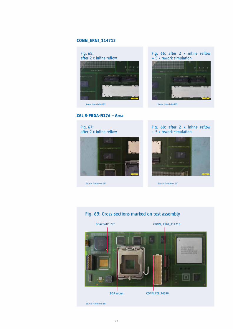
73
CONN_ERNI_114713
ZAL R-PBGA-N176 – Area
Fig. 69: Cross-sections marked on test assembly
Source: Fraunhofer ISIT
Fig. 65: after 2 x inline reflow
Fig. 66: after 2 x inline reflow + 5 x rework simulation
Source: Fraunhofer ISIT Source: Fraunhofer ISIT
Fig. 67: after 2 x inline reflow
Fig. 68: after 2 x inline reflow + 5 x rework simulation
Source: Fraunhofer ISIT Source: Fraunhofer ISIT
BGA256TI1.27C CONN_ ERNI_114713
BGA socket CONN_FCI_74390

74
4.5.2 Cross-sectional analysis of printed circuit assemblies after multiple solder stresses In addition to visual inspection, cross-sec-tional analysis yields more insight into the nature of the zones impacted by multiple solder stresses.
The following components and correspond-ing areas of the circuit board were inves-tigated using cross-sectional analysis - see Figure 69 and Table 13.
Components Thermal stress Assessment1
BGA256TI1.27C 2 x inline reflow+
2 x rework simulation
No significant abnormalities with respect to internal PCB or com-ponent damage such as delamination, damage to the laminate or sleeve, pad cratering, pad lifts etc. - assessing solder junctions was not the priority during this step of investigation.
BGA256TI1.27C 2 x inline reflow+
5 x rework simulation
Circuit board under BGA256TI1.27C
2 x inline reflow+
5 x rework simulation
BGA socket 2 x inline reflow+
5 x rework simulation
Circuit board under BGA socket
2 x inline reflow+
5 x rework simulation
CONN_FCI_74390 2 x inline reflow+
2 x rework simulation
CONN_ ERNI_114713 2 x inline reflow+
5 x rework simulation
ZAL R-PBGA-N176 2 x inline reflow+
2 x rework simulation
Microvia under ZAL R-PBGA-N176
2 x inline reflow+
2 x rework simulation
ZAL R-PBGA-N176 2 x inline reflow+
5 x rework simulation
Microvia under ZAL R-PBGA-N176
2 x inline reflow+
5 x rework simulation
Circuit board under ZAL R-PBGA-N176
2 x inline reflow+
5 x rework simulation
Through-hole plating under Z-S-PQFP-G100
2 x inline reflow+
2 x rework simulation
Tab. 13: Overview of the components and corresponding circuit board areas inspected with cross-sectional analysis following thermal stress
1 In the process of extreme soldering heat stresses repeated on the same component, wetting faults and non-conforming solder joints may arise, which are not accounted for in the assessment.

75
Components Remarks Number of rework simulations
BGA256TI1.27C Left corner shows control pad without BGA ball
2 x
BGA256TI1.27C Centre of component, dewetting beginning component side on the right ball
5 x
Circuit board under BGA256TI1.27C
No abnormalities
5 x
BGA socket Ageing effects in micro-structure
5 x
Circuit board under BGA socket
No abnormalities
5 x
Tab. 14: Cross-sectional analysis of components and corresponding circuit board areasaftertwo-passinlinereflowandtwo-orfive-passreworksimulation
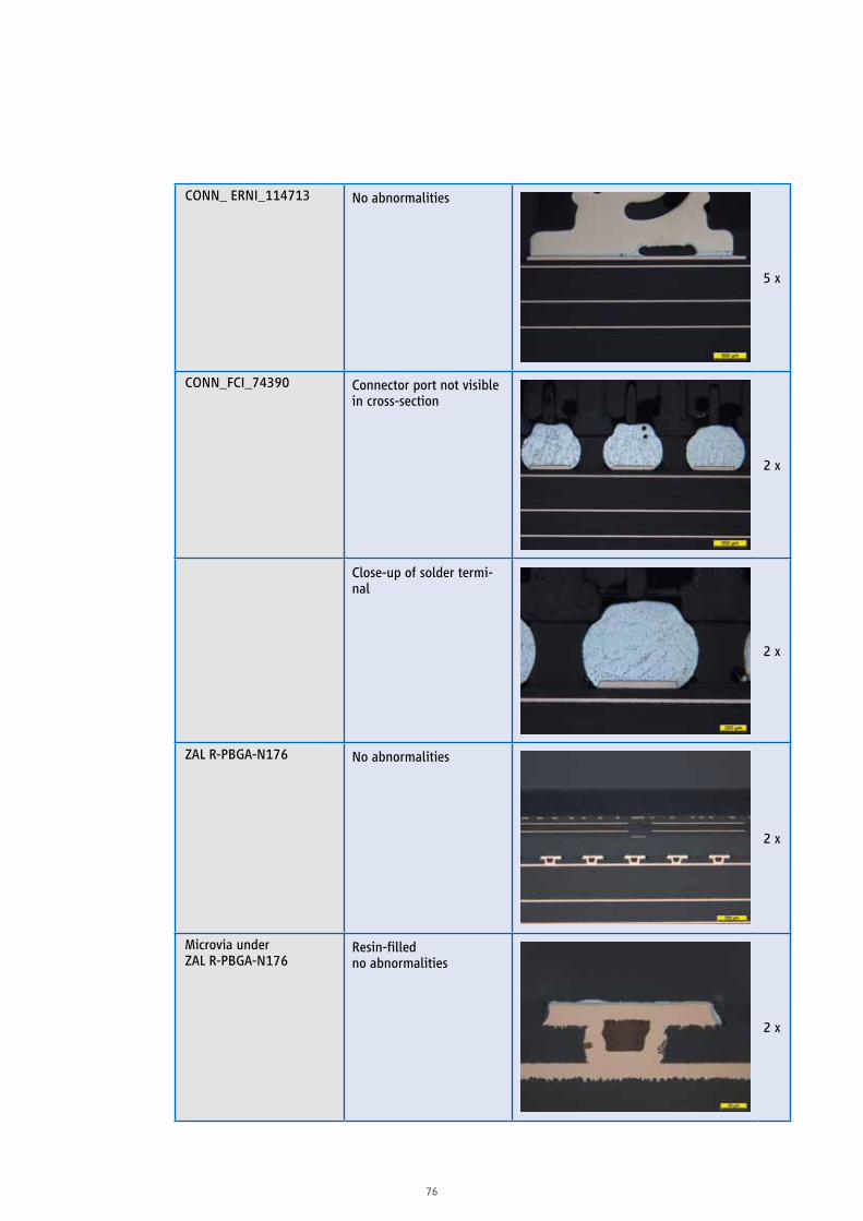
76
CONN_ ERNI_114713 No abnormalities
5 x
CONN_FCI_74390 Connector port not visible in cross-section
2 x
Close-up of solder termi-nal
2 x
ZAL R-PBGA-N176 No abnormalities
2 x
Microvia under ZAL R-PBGA-N176
Resin-filled no abnormalities
2 x

77
Components Remarks Number of rework simulations
ZAL R-PBGA-N176 No abnormalities
2 x
Microvia under ZAL R-PBGA-N176
No abnormalities follow-ing reflow cycles, except for noticeable fill level in microvia
2 x
ZAL R-PBGA-N176 No abnormalities
5 x
Microvia under ZAL R-PBGA-N176
No abnormalities follow-ing reflow cycles, except for noticeable fill level in microvia
5 x
Circuit board under ZAL R-PBGA-N176
No abnormalities
5 x

78
Microvia (resin-filled) under ZAL R-PBGA-N176
No abnormalities follow-ing reflow cycles, except for incomplete Ni/Au covering of the pad
5 x
Through-hole plating under Z-S-PQFP-G100
No abnormalities
2 x
Through-hole plating under Z-S-PQFP-G100
Close-up of through-hole plating, no abnormalities
2 x
Close-up of through-hole plating under Z-S-PQFP-G100
Close-up of upper through-hole plating, no abnormalities
2 x
Through-hole plating under Z-S-PQFP-G100
Close-up of lower through-hole plating, no abnormalities
2 x
Source: Fraunhofer ISIT
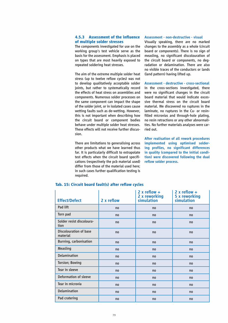
79
4.5.3 Assessmentoftheinfluenceof multiple solder stresses The components investigated for use on the working group's test vehicle serve as the basis for the assessment. Emphasis is placed on types that are most heavily exposed to repeated soldering heat stresses.
The aim of the extreme multiple solder heat stress (up to twelve reflow cycles) was not to develop qualitatively acceptable solder joints, but rather to systematically record the effects of heat stress on assemblies and components. Numerous solder processes on the same component can impact the shape of the solder joint, or in isolated cases cause wetting faults such as de-wetting. However, this is not important when describing how the circuit board or component bodies behave under multiple solder heat stresses. These effects will not receive further discus-sion.
There are limitations to generalising across other products what we have learned thus far. It is particularly difficult to extrapolate test effects when the circuit board specifi-cations (respectively the pcb material used) differ from those of the material used here; in such cases further qualification testing is required.
Assessment - non-destructive - visual Visually speaking, there are no marked changes to the assembly as a whole (circuit board or components). There is no sign of measling, no significant discolouration of the circuit board or components, no deg-radation or delamination. There are also no visible traces of the conductors or lands (land pattern) having lifted up.
Assessment - destructive - cross-sectionalIn the cross-sections investigated, there were no significant changes in the circuit board material that would indicate exces-sive thermal stress on the circuit board material. We discovered no ruptures in the laminate, no ruptures in the Cu- or resin-filled microvias and through-hole plating, no resin retractions or any other abnormali-ties. No further materials analyses were car-ried out.
After realisation of all rework procedures implemented using optimised solder-ing profiles, no significant differencesin quality (compared to the initial condi-tion)werediscovered following thedualreflowsolderprocess.
Effect/Defect 2xreflow
2xreflow+ 2 x reworking simulation
2xreflow+ 5 x reworking simulation
Pad lift no no no
Torn pad no no no
Solder resist discoloura-tion
no no no
Discolouration of base material
no no no
Burning, carbonisation no no no
Measling no no no
Delamination no no no
Torsion; Bowing no no no
Tear in sleeve no no no
Deformation of sleeve no no no
Tear in microvia no no no
Delamination no no no
Pad cratering no no no
Tab.15:Circuitboardfault(s)afterreflowcycles
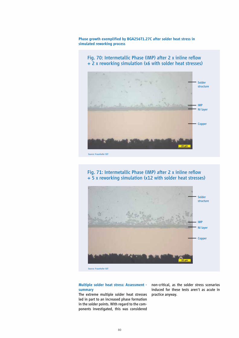
80
Multiple solder heat stress: Assessment - summaryThe extreme multiple solder heat stresses led in part to an increased phase formation in the solder points. With regard to the com-ponents investigated, this was considered
non-critical, as the solder stress scenarios induced for these tests aren't as acute in practice anyway.
Fig. 70: Intermetallic Phase (IMP) after 2 x inline reflow + 2 x reworking simulation (x6 with solder heat stresses)
Source: Fraunhofer ISIT
Solder structure
Ni layer
Copper
IMP
Fig. 71: Intermetallic Phase (IMP) after 2 x inline reflow + 5 x reworking simulation (x12 with solder heat stresses)
Source: Fraunhofer ISIT
Solder structure
Ni layer
Copper
IMP
PhasegrowthexemplifiedbyBGA256T1.27Caftersolderheatstressinsimulated reworking process
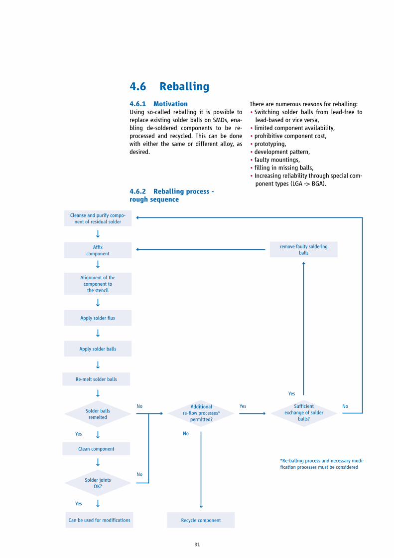
81
4.6 Reballing4.6.1 MotivationUsing so-called reballing it is possible to replace existing solder balls on SMDs, ena-bling de-soldered components to be re-processed and recycled. This can be done with either the same or different alloy, as desired.
There are numerous reasons for reballing:• Switching solder balls from lead-free to
lead-based or vice versa,• limited component availability,• prohibitive component cost,• prototyping, • development pattern,• faulty mountings,• filling in missing balls, • Increasing reliability through special com-
ponent types (LGA -> BGA).4.6.2 Reballing process - rough sequence
Cleanse and purify compo-nent of residual solder
Affix component
remove faulty soldering balls
Alignment of the component to
the stencil
Apply solder balls
Apply solder flux
Can be used for modifications Recycle component
Re-melt solder balls
Clean component
Solder joints OK?
Solder balls remelted
Additional re-flow processes*
permitted?
Sufficient exchange of solder
balls?
*Re-balling process and necessary modi-fication processes must be considered
Yes
Yes
Yes
No No
No
No
Yes

82
4.6.3 Devices - Systems - SchemesFollowing are descriptions of devices and concepts which are employed variously according to throughput, task and batch size.
Reballing set Reballing system Laser balling
Ball positioning stencil stencil X-Y axis system
Flexibility Balling process
entire surface entire surface selective
Typical component count per cycle
single piece single piece or multi-use
single piece or multi-use
Footprint 300 × 150 mm² 300 × 400 mm² >2 m²
Position correction (Balls to component)
fixed adjustable automatic
Typical processing sur-face area [mm²]
80 x 80 100 x 150 150 x 150/300 x 300
Applicability for high batch sizes
low medium low to medium
System cost low medium very high
Cost to operate low low high
Component finish level after processing
solder balls must still be
re-melted in reflow
solder balls must still be
re-melted in reflow
solder balls already re-melted by laser
soldering
Microvia - tear no no no
Delamination no no no
Pad cratering no no no
Tab. 16: Typical parameters of reballing schemes
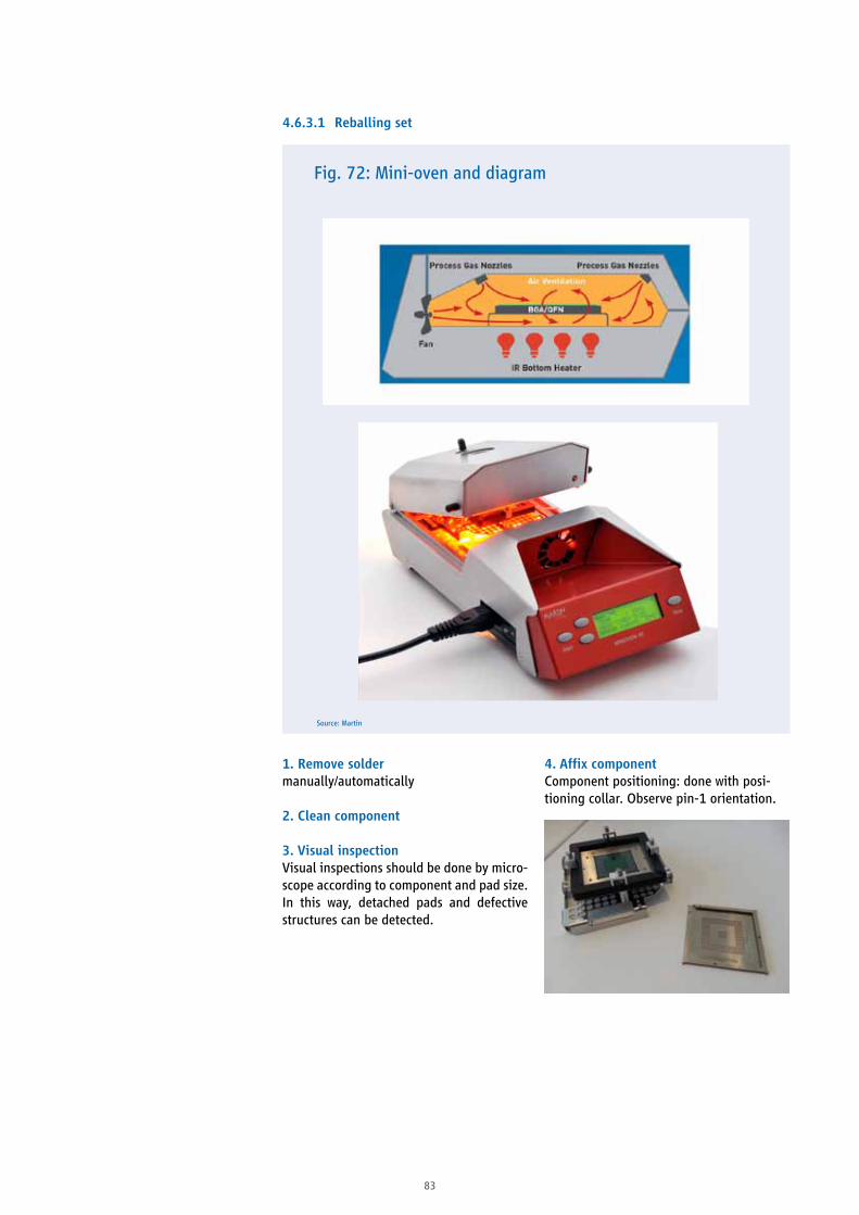
83
4.AffixcomponentComponent positioning: done with posi-tioning collar. Observe pin-1 orientation.
1. Remove solder manually/automatically
2. Clean component
3. Visual inspection Visual inspections should be done by micro-scope according to component and pad size. In this way, detached pads and defective structures can be detected.
Fig. 72: Mini-oven and diagram
Source: Martin
4.6.3.1 Reballing set
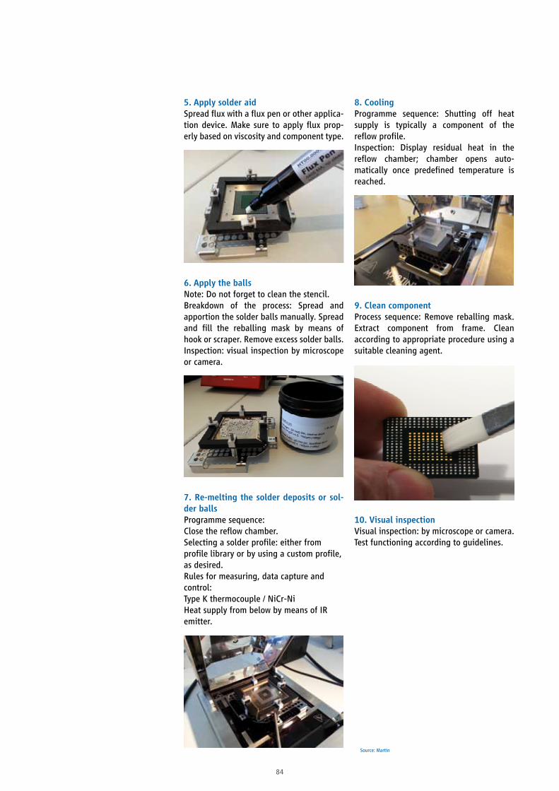
84
5. Apply solder aidSpread flux with a flux pen or other applica-tion device. Make sure to apply flux prop-erly based on viscosity and component type.
6. Apply the balls Note: Do not forget to clean the stencil.Breakdown of the process: Spread and apportion the solder balls manually. Spread and fill the reballing mask by means of hook or scraper. Remove excess solder balls.Inspection: visual inspection by microscope or camera.
7. Re-melting the solder deposits or sol-der balls Programme sequence: Close the reflow chamber.Selecting a solder profile: either from profile library or by using a custom profile, as desired.Rules for measuring, data capture and control: Type K thermocouple / NiCr-Ni Heat supply from below by means of IR emitter.
Source: Martin
8. CoolingProgramme sequence: Shutting off heat supply is typically a component of the reflow profile. Inspection: Display residual heat in the reflow chamber; chamber opens auto-matically once predefined temperature is reached.
9. Clean component Process sequence: Remove reballing mask. Extract component from frame. Clean according to appropriate procedure using a suitable cleaning agent.
10. Visual inspection Visual inspection: by microscope or camera. Test functioning according to guidelines.

85
4.6.3.2 Reballing system
The reballing system uses gravity feeding to place solder balls on circuit boards and BGAs. This system was designed for rework prototyping and small serial production.
This mechanically operating system offers accurate and adjustable positioning and fixing capacities; orientation of the stencil openings towards the substrate; and defined location positioning. It features a high degree of precision and reproducibility.
In this ball placement procedure, solder balls are spread evenly over a stencil. For this purpose, the stencil with its balling grid is placed over the product, which already has been printed with flux by means of another stencil. The stencil has a precisely defined balling pattern reflecting the pads on either the circuit board or the compo-nent. The figure below schematically depicts the arrangement of substrate, flux deposits and stencil with balling pattern.
The component is fixed in place using an easily exchangeable vacuum plate. In this process the component is loaded [onto the vacuum plate], roughly oriented, and then fixed in place by vacuum. The stencils needed for positioning the solder balls are clamped in a clamping frame and are easy to replace. The arrangement also allows one to remove the entire clamping frame, allow-ing for easy swaps between the flux applica-tion stencil and the solder ball placement stencil. This construction enables a highly flexible manufacturing process and makes it possible to rework a wide variety of com-ponent models.
The pads of Loose components can be aligned to stencil openings (for the solder balls) using an X-Y positioning unit. A pre-cise camera system, outputted to an LCD display, assists the user in aligning the com-ponent to the stencil, ensuring fast and sim-ple operation. Differing component depths
Fig. 73: Reballing system
Source: Wagenbrett
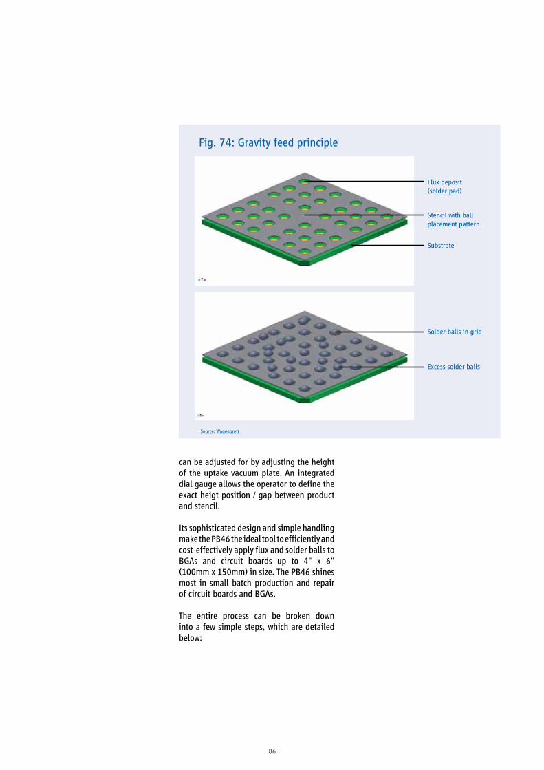
86
can be adjusted for by adjusting the height of the uptake vacuum plate. An integrated dial gauge allows the operator to define the exact heigt position / gap between product and stencil.
Its sophisticated design and simple handling make the PB46 the ideal tool to efficiently and cost-effectively apply flux and solder balls to BGAs and circuit boards up to 4" x 6" (100mm x 150mm) in size. The PB46 shines most in small batch production and repair of circuit boards and BGAs.
The entire process can be broken down into a few simple steps, which are detailed below:
Fig. 74: Gravity feed principle
Source: Wagenbrett
Flux deposit (solder pad)
Stencil with ball placement pattern
Substrate
Excess solder balls
Solder balls in grid

87
1. Set up the vacuum plateUnique vacuum plates allow the component to be loaded and fixed in place, and can easily be swapped. Here, a component up to 4" x 6" (100mm x 150mm) in size can be loaded.
2. Set up the stencil cover By opening the hinge, the stencil together with its cover can easily be lifted out and exchanged.By loosening the knurled screws the clamp-ing frame can be lifted up and the stencil rapidly swapped.
3. Fix the component onto the vacuum plateThe component is fixed in the defined posi-tion with the help of vacuum suction,and its position in the x-y plane can be adjusted.
4.ApplyfluxFlux is applied and reaches the component through the openings in the stencil.Stencil thickness determines the amount of flux deposits.
5. Deposit solder ballsAfter the stencil has been replaced, spread the solder balls over the stencil. As the work table of the device tilts, the solder balls roll over the stencil, fall through the openings and stick to the previously-applied flux.
6. Cleaning processAfter the flux is applied the stencil is cleaned.If a visual inspection shows that the ball-ing process has contaminated the stencil, it must be cleaned again.
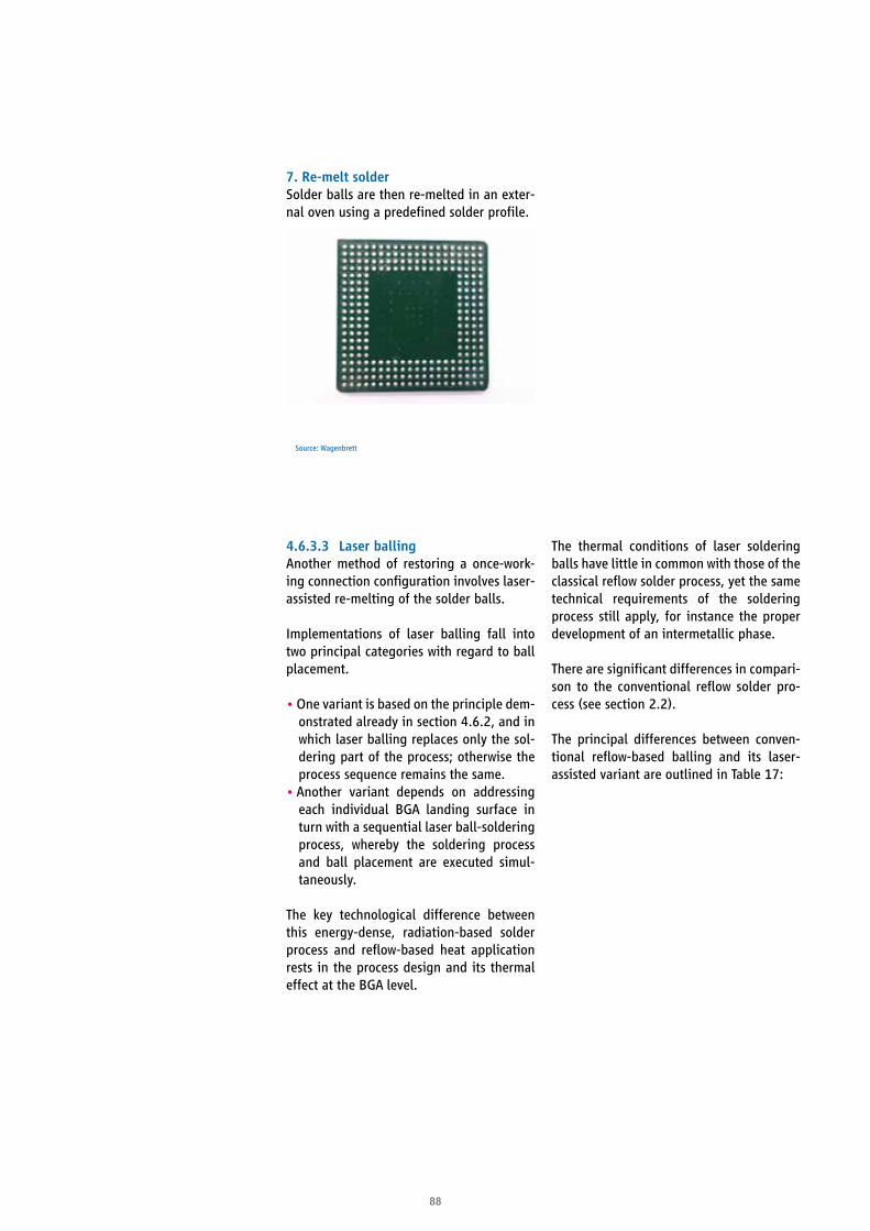
88
4.6.3.3 Laser ballingAnother method of restoring a once-work-ing connection configuration involves laser-assisted re-melting of the solder balls.
Implementations of laser balling fall into two principal categories with regard to ball placement.
• One variant is based on the principle dem-onstrated already in section 4.6.2, and in which laser balling replaces only the sol-dering part of the process; otherwise the process sequence remains the same.
• Another variant depends on addressing each individual BGA landing surface in turn with a sequential laser ball-soldering process, whereby the soldering process and ball placement are executed simul-taneously.
The key technological difference between this energy-dense, radiation-based solder process and reflow-based heat application rests in the process design and its thermal effect at the BGA level.
The thermal conditions of laser soldering balls have little in common with those of the classical reflow solder process, yet the same technical requirements of the soldering process still apply, for instance the proper development of an intermetallic phase.
There are significant differences in compari-son to the conventional reflow solder pro-cess (see section 2.2).
The principal differences between conven-tional reflow-based balling and its laser-assisted variant are outlined in Table 17:
Source: Wagenbrett
7. Re-melt solderSolder balls are then re-melted in an exter-nal oven using a predefined solder profile.

89
Solder procedure "Balling" Conventionalreflow Laser-assisted
Basis for developing solder profile
Standard solder profile (e.g. based on DIN EN 61760-1 [2] or IPC-7095 [6]), optimised for the respective component housing where applicable
Custom profile develop-ment in order to match the unique heat transfer characteris-tics of laser soldering
Parameters and duration of heat input
Gradients, dwell times, peak temperature. Typi-cally in the range of 3-5 minutes.
Component pre-heating where appropriate. Con-tinuous pre-heating, laser impulse (timed), laser energy lasting albeit only fractions of a second.
Time above liquidus Typically 30-90 seconds Typically on the orderof seconds
Principle of heat trans-mission
Heat supply by way of full convection, radiation or condensation
Direct radiative heat injec-tion to the molten ball, with transmission by direct conductive contact with the component's pad
Typical soldering area Solder heat paradigm applies to the entire com-ponent
Individual solder area selection
Temperature, upper sur-face of component
Approximately identical to temperature on compo-nent underside
In the range of the selected pre-heating
Process time per compo-nent
Identical to selected reflow profile 3-5 minutes
Depends on mode selected (full-surface balling or single ball).For example, approx. 2 minutes for PBGA 256
Process time per connec-tion
Identical to selected reflow profile 3-5 minutes
Values are typically 0.5 seconds per ball + pos-sible pre-heating
Primary risks "Using up" a reflow life - manufacturers typically provide for 3 reflow cycles (J-STD-020 [3])
The component itself undergoes locally very limited solder heat input (lower than with gentle, point-by-point pad resto-ration by hand)
Secondary risks As in conventional mount-ing processes, MSL must also be observed.
Typical laser profiles do not require that MSL be observed.
Tab.17:Comparisonofreflow-andlaser-basedsoldering

90
Advantages Established sub-proce-dures constitute basis for implementation. No need to rethink materi-als selection, durability or process characteristics. Readily available. Cost-effective. Solder profiles often already exist.No need for a separate workstation.
After optimised parametrisation:High reproducibility and simultaneous minimisa-tion of solder stress is attainable.Relatively short process times for BGAs with few balls.Time- and temperature-optimised treatment for individual balls possible.
Disadvantages Negligible difference in process times between small and large compo-nent types (i.e. between few and many balls).Requires complete addi-tional reflow cycle.
Costly.Few documents, standards and guidelines currently available for reference (GEIA-STD-0015) [53].Requires separate worksta-tionExpertise in conventional assembly process usually not especially pronounced.
Fig. 75: Laser placement head over component pad positions to be balled
Source: Airbus DS Electronics and Border Security

91
4.6.4 Balling stencilsBalling stencils are used to place solder spheres on a component. The first step is to print flux at the component. The purpose of the flux is twofold:
1. To provide a sufficient amount of activa-tors for the soldering process.
2. To provide enough sticking power to keep the solder ball in position until the soldering process is complete.
This is followed by positioning the solder balls with a stencil. The stencil openings are designed so that only one ball fits inside, and other balls on the stencil's surface won't catch when they slide off.
4.6.5 Reballing - Recommenda-tions for the process sequence
Step in process Possible risks Recommendation
Removing residual solder Overheating destroys component Damage to or separation of pads due to overheat-ing and/or physical impact
Observe the component's temperature limits, use contactless reflow-based solder residue removal, use flux.
Cleaning the component (where required)
No or insufficient clean-ing, with inappropriate processes or substances
Use appropriate cleaning process.
Inserting the component Use of the wrong position-ing frame
Accurate documentation and work directives
Applying solder Application of excessive solder can allow balls to change position during re-melting. Insufficient solder applica-tion can lead to wetting errors.
Targeted application using suitable procedure
Setting stencil + balling Using the wrong balls (size, alloy) or stencil
Accurate documentation and work directives
Re-melting Use of solder process not suited to heating require-ments
Use of profile not adjusted for flow requirements
Use a suitable reflow pro-file (adapted to the speci-fications from solder mate-rial, flux and component manufacturer recommen-dations).
Reduce flow velocity, increase flux adhesiveness, use a stencil during re-melting.
Tab. 18: Reducing risks during the reballing process

92
Releasing the component After the re-melting step, flux can cause the stencil to stick to the component. Use of tools (scalpels, etc.) or excessive force can result in damage when removing the component.
In addition, the solder may become stuck to the sten-cil during soldering. When lifting the component out, there is a danger of tearing off the pad(s).
With fine-pitch stencils or stencils with extensive grid arrays, heat exposure can lead to tensions between the balls and the stencil.
By using the right flux removal, it is possible to remove the component with a minimum of force.
Regular cleaning (suitable cleaning fluid, ultrasonic bath in cases of heavy soiling) and replacing the stencil at regular intervals will prevent sticking.
By using appropriate sten-cil technologies approved for use in soldering pro-cesses, waste due to heat-induced stresses can be avoided.
4.7 Stencil and process technology4.7.1 Rework stencils for printing on circuit boards
4.7.1.1 ApplicationRework stencils allow for a circuit board printing predominantly limited to one com-ponent; or the printing of one component with solder paste before it is put on the assembly. In this way the volume of solder necessary for the solder joint is provided, so that the component can be selectively sol-dered onto a complete assembly.
Rework stencils fall into three groups:1. Stencils for selectively printing single
and pattern on an already populated circuit board.
2. Stencils for the printing directly on com-ponents.
3. Stencils or apparatus for dipping com-ponents.
Stencils are used to provide solder paste to a vacated mounting position on an already finished assembly following removal of a component, to prepare for the rework sol-dering process.
Here the stencil has multiple functions:1. Preparing the right amount of solder
paste together with a reproducible printable combination of opening sizes and stencil thicknesses.
2. Protecting the assembly against solder paste contamination during manual printing, for example by upwards-turned stencil edges.
3. Maintaining the position at the land pattern. By means of brackets for rework systems or by using circuit board guides, e.g. positioning holes.
4.7.1.2 Rework stencil designThe stencil's key feature are the openings for the component land pattern. If the causes of failure are known and lie in the initial layout, adjustments should be made in order to avoid future failures.
The distance between the paste shield and the opening is selected depending on the available space around the mounting place being worked on. The larger the gap can be made here, the easier manual printing will be later on.

93
Such stencils are usually taken up by rework systems, to orient and position them on the circuit board. Depending on the rework system the stencil has to handle various mounting brackets.
Corresponding design documents on the form and execution of the brackets should be submitted when ordering such stencils.
If the stencil is to be positioned manually during printing, holes (if present), or the outer edge of the circuit board can be used to secure its position. These data should also be supplied when ordering such stencils.
Should the prescribed sizes of the circuit board pads or component pads not be observed, the solder paste transfer could be affected. In this regard, it is critical if the pad is too small, there may not be enough contact area for the solder paste during printing. In this way the solder paste may become (partially) stuck in the aper-ture of the stencil due to insufficient adhe-sion (pad-to-solder paste). Consequences include weak solder connections with low solder volume.
The flatness of the circuit board likewise plays a major role. If the solder resist pro-trudes too far above the pad surface, the lift (snap-off) created by the unevenness may well lead to an increased volume of solder paste being applied. With the heatsink area in particular, increased volume can result in the component drifting or tipping.
If the protrusions underneath the com-ponent are pronounced, it is important to ensure that the component receives enough solder paste to build up sufficiently high solder connections, which will fully fill the space between component and circuit board.
In both cases it is recommended to calculate the amount of paste needed so that there is sufficient solder volume to ensure complete wetting over the connection surfaces at the required solder joint height.
4.7.1.3 BenefitThis type of stencil allows paste applica-tion with components that can't be directly printed, e.g. components with delicate leads that may buckle during printing.
Fig. 76: Stencil with bracket for use in a rework system
Source: Zevac
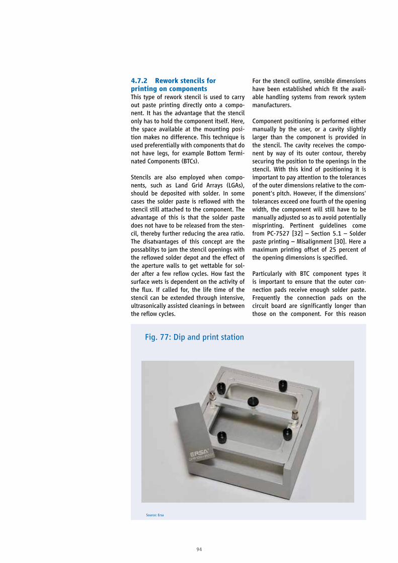
94
4.7.2 Rework stencils for printing on componentsThis type of rework stencil is used to carry out paste printing directly onto a compo-nent. It has the advantage that the stencil only has to hold the component itself. Here, the space available at the mounting posi-tion makes no difference. This technique is used preferentially with components that do not have legs, for example Bottom Termi-nated Components (BTCs).
Stencils are also employed when compo-nents, such as Land Grid Arrays (LGAs), should be deposited with solder. In some cases the solder paste is reflowed with the stencil still attached to the component. The advantage of this is that the solder paste does not have to be released from the sten-cil, thereby further reducing the area ratio. The disatvantages of this concept are the possablitys to jam the stencil openings with the reflowed solder depot and the effect of the aperture walls to get wettable for sol-der after a few reflow cycles. How fast the surface wets is dependent on the activity of the flux. If called for, the life time of the stencil can be extended through intensive, ultrasonically assisted cleanings in between the reflow cycles.
For the stencil outline, sensible dimensions have been established which fit the avail-able handling systems from rework system manufacturers.
Component positioning is performed either manually by the user, or a cavity slightly larger than the component is provided in the stencil. The cavity receives the compo-nent by way of its outer contour, thereby securing the position to the openings in the stencil. With this kind of positioning it is important to pay attention to the tolerances of the outer dimensions relative to the com-ponent's pitch. However, if the dimensions' tolerances exceed one fourth of the opening width, the component will still have to be manually adjusted so as to avoid potentially misprinting. Pertinent guidelines come from PC-7527 [32] – Section 5.1 – Solder paste printing – Misalignment [30]. Here a maximum printing offset of 25 percent of the opening dimensions is specified.
Particularly with BTC component types it is important to ensure that the outer con-nection pads receive enough solder paste. Frequently the connection pads on the circuit board are significantly longer than those on the component. For this reason
Fig. 77: Dip and print station
Source: Ersa

95
it can become difficult to receive the same amount of solder in component printing as was used in the PCB printing. This is pos-sible by overprinting the component pads and adjusting the thickness of the stencil, but the release of the solder paste must be checked by the area ratio.
If a rework is necessary due to a tipped com-ponent with open solder joints on some of the outer pads, the cause may lie in the sol-der paste layout of the thermal pad. If the thermal pad is given too much solder, the component may float, thus lifting the outer connection points on one or more sides. In such cases it is recommended to reduce the solder volume of the thermal pad. Thermal pads of QFN component types are typically pasted over 25 to 65 percent of their wetta-ble surface area. 50 percent of the wettable area is an established figure. If this value does not produce acceptable results, it may help to refer to the stencil manufacturer for a calculation of the needed solder volume.
Other causes for tipping can include extreme voids, extreme variance in pad sizes or unevenness in the circuit board.
Larger voids, because of the volume they take in, create a change in the form of the solder joint, primarily through a change in the solder gap. X-ray analysis helps shed light on the actual state of the solder joint.
4.7.3 Rework stencils for compo-nent dippingComponents whose connections lie on their undersides and stick out of the component body (e.g. BGA types) can be dipped. This involves immersing them with their con-nections in a film of flux of solder paste. When the component is lifted out, the dip-ping medium sticks to the connections and is then available to assist the formation of the solder joint. The amount of dipping medium that sticks to a component connection depends mainly on the form of the connection and the immer-sion depth. Dipping stencils are designed so that the depth of the cavity matches the immersion depth, so as to minimise process fluctuations.
Fig. 78: Rework stencil for QFN component (Quad Flat pack No leads)
Source: Ersa

96
Dipping stencils allow for a reproducible volume application on the component with-out having to produce a component-specific stencil. Various types of SMD component can be dipped, but in gull-wing leads for example, volume application ends up being fairly low.
Fig. 79: Dip stencil, filled with flux
Source: Ersa
Fig. 80: BGA ball after being dipped in solder paste
Source: Ersa

97
4.7.4 Process techniqueThe following sequence shows direct print-ing following the example of a BTC.
Fig. 81: QFN printing sequence, variant 1
Source: Ersa
A Handling tool with stencil inserted and component on top
B The component is inserted into the stencil and fixed in place
C Component inserted in toolD The carrier frame is turned over for printingE Printing the componentF Printing complete
G The stencil is inserted with component into the rework system
H The fixing arm is pivoted away and the component is picked up with the pick and place head
I The printed component can now be positioned and placed
Generalnotes• Note the orientation of pin-1 when align-
ing the component.• During manual printing, note the squee-
gee force and blade angle.• After printing, visually inspect the level of
filling.• Pay attention to completly wipe the print
area clean with your print stroke.• A minimum of force is recommended
when placing the component onto the cir-cuit board.
• Clean the stencil with a suitable medium. In case of heavy contermination on the stencil, clean in an ultrasonic bath.
CB
D E
H I
A
F
G

98
Fig. 82: QFN printing sequence, variant 2
Source: Martin
A BTC printing tool with stencil receptacle, hold-down device, printing stencil, compo-nent
B Insert stencil and componentC Fix component in place by closing the
magnetic hold-down deviceD Apply the right amount of solder paste
(cartridge, scoop)
E Solder paste in position for printingF Printing the solder paste with a hand
scraper G Result after printingH Insert BTC printing tool into rework system;
remove hold-down device before removing component
I Machine-assisted component removal
Fig. 83: QFN printing sequence, variant 3
Source: Zevac
A Handling tool with stencil insertedB The component is positioned in the stencilC Component inserted in tool
and fixed in placeD The carrier frame is turned over for printingE Printing the componentF Printing complete
G The carrier frame with printed component is inserted into the machine
H The fixing arm is pivoted away and the component with mounting head is removed
I The printed component can now be positioned and mounted
C
C
B
B
D
D
E
E
H
H
I
I
A
A
F
F
G
G
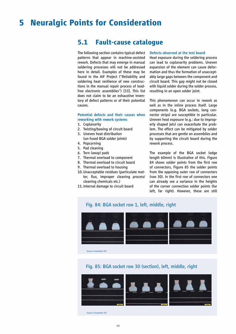
99
5 Neuralgic Points for Consideration
The following section contains typical defect patterns that appear in machine-assisted rework. Defects that may emerge in manual soldering processes will not be addressed here in detail. Examples of these may be found in the AiF Project ("Reliability and soldering heat resilience of new construc-tions in the manual repair process of lead-free electronic assemblies") [33]. This list does not claim to be an exhaustive inven-tory of defect patterns or of their potential causes.
Potential defects and their causes when reworking with rework systems1. Coplanarity2. Twisting/bowing of circuit board3. Uneven heat distribution (un-fused BGA solder joints)4. Popcorning 5. Pad cleaning6. Torn (away) pads7. Thermal overload to component8. Thermal overload to circuit board9. Thermal overload to housing10. Unacceptable residues (particulate mat-
ter, flux, improper cleaning process/cleaning chemicals etc.)
11. Internal damage to circuit board
Defects observed at the test boardHeat exposure during the soldering process can lead to coplanarity problems. Uneven expansion of the element can cause defor-mation and thus the formation of unaccept-ably large gaps between the component and circuit board. This gap might not be closed with liquid solder during the solder process, resulting in an open solder joint.
This phenomenon can occur in rework as well as in the inline process itself. Large components (e.g. BGA sockets, long con-nector strips) are susceptible in particular. Uneven heat exposure (e.g.: due to improp-erly shaped jets) can exacerbate the prob-lem. The effect can be mitigated by solder processes that are gentle on assemblies and by supporting the circuit board during the rework process.
The example of the BGA socket (edge length 60mm) is illustrative of this. Figure 84 shows solder points from the first row of connectors, Figure 85 the solder points from the opposing outer row of connectors (row 30). In the first row of connectors one can already see a variance in the heights of the corner connection solder points (far left, far right). However, these are still
5.1 Fault-cause catalogue
Fig. 84: BGA socket row 1, left, middle, right
Source: Fraunhofer ISIT
Fig. 85: BGA socket row 30 (section), left, middle, right
Source: Fraunhofer ISIT

100
within acceptable limits. On the opposite side (Figure 85) the differences are more pronounced. The open solder joint can be clearly seen (close-up in Figure 86), which can be traced back to a deformation of the component during the soldering process.
Excessive heat exposure during the removal of residual solder can result in exposure of the intermetallic phase on the circuit board
pad. This is no longer wettable and inhib-its a firmly bonded connection during the soldering process (Figures 87, 88). This wetting defect is difficult or impossible to verify non-invasively (e.g. by X-ray), making it easy to overlook. This defect mode can be avoided by using a gentle and, if possible, contact-free solder residue removal process.
Fig. 86: BGA socket, ball separation due to coplanarity defect, close-up
Source: Fraunhofer ISIT
Fig. 87: ZAL R-PBGA-N176, wetting defect, overview
Source: Fraunhofer ISIT

101
Fig. 88: ZAL R-PBGA-N176, wetting defect, close-up
Source: Fraunhofer ISIT
Fig. 89: ZAL R-PBGA-N176, deformed solder joints
Source: Fraunhofer ISIT

102
In the case of insufficient soldering heat, not all solder points will be in a molten state for a sufficient length of time. This results in the component not being able to swim into position. Should the solder solid-ify in this position, the result is an improp-erly mounted component (Figures 89, 90). The proper temperature profile will help to prevent this defect.
Other typical defect patterns from manual-solderingIn light of the number of ways that manual-soldering can be executed, the resulting defect patterns can manifest in an equally diverse manner. Based on defect type and frequency, the defect in question may be systematic or random.
In the following, typical defect modes occur-ring during manual soldering will be used to demonstrate the correlation between defect patterns and their common causes and to suggest mitigation strategies. This list does not claim to be exhaustive, nor is it the last word with regard to correlations between faults, fault causes, and their prevention. Rather, the following overview is intended as a practical reference for the purpose of more readily identifying the cause(s) of defects.
In all manual soldering processes, particular attention should be paid to the functional interplay between operator and machine.
Thus, the dominant factor (besides power, thermal control characteristics and sensible device set-up) in the results of hand solder-ing processes is the trained, professional handling of the soldering device.
Fig. 90: ZAL R-PBGA-N176, deformed solder joints, close-up
Source: Fraunhofer ISIT

103
Source: Fraunhofer ISIT
Fig. 91: SOT23, acceptable manu-ally soldered junction (top right)
Fig. 92: Acceptable solder joint with undamaged component, but with first signs of damage to lami-nate (delamination)
Source: Fraunhofer ISIT
Causes:Too much heat exposure on critical areas
Prevention:Training.Adjust soldering tip geometry.Monitor soldering tip temperature
Causes:Too much solder used during manual-soldering
Prevention:While not necessarily required with the pic-tured component type (SOT23), theuse of thinner solder wire and/or better soldering tip shape is recommended
Defect / Causes / Prevention
Source: Fraunhofer ISIT
Fig. 93: Tear in laminate / not vis-ible from surface
Fig. 94: Delamination of internal layer / not visible from surface
Source: Fraunhofer ISIT
Cause:Soldering tip temperature too high and/or contact period too long
Prevention:Training. Controlled soldering tip temperature and suitable soldering tip shape.Simultaneous heating from underside to pre-heat assembly
Cause:Soldering tip temperature too high and/or contact period too long
Prevention:Training. Controlled soldering tip temperature and suitable soldering tip shape. Simultaneous heating from underside to pre-heat assembly

104
Source: Fraunhofer ISIT
Fig. 95: Pad lifting with tear in laminate due to excessive solder-ing time, barely visible
Fig. 96: Resin content of the circuit board beginning to fuse, barely visible (danger of confusion with flux residues)
Source: Fraunhofer ISIT
Cause:Temperature of solder or soldering tip too high and/or contact period too long
Prevention:Training. Controlled soldering tip temperature and suitable soldering tip shape. Simultaneous heating from underside to pre-heat assembly
Note:Use of circuit board materials with high T
D
value could reduce this effect.
Cause:Temperature of solder or soldering tip too high and/or contact period too long
Prevention:Training. Controlled soldering tip temperature and suitable soldering tip shape. Simultaneous heating from underside to pre-heat assembly
Note:This effect could be further reduced by use of z-axis CTE-optimised circuit board materials.
Source: Fraunhofer ISIT
Fig. 97: Pad lifting due to exces-sive soldering tip temperature
Fig. 98: Pad lifting due to excessive mechanical pressure
Source: Fraunhofer ISIT
Cause:Excessive pressure whilst applying solder and/or contact times too long
Prevention:Training. Suitable soldering tip geometry; ide-ally, monitor heat exposure through the molten solder.Simultaneous heating from underside to pre-heat assembly
Note:HF-capable circuit board materials in particular tend to have reduced bond strength (peel strength).
Cause:Soldering tip temperature too high and/or contact period too long
Prevention:Training. Controlled soldering tip temperature and suitable soldering tip shape. Simultaneous heating from underside to pre-heat assembly
Note:HF-capable circuit board materials in particular tend to have reduced bond strength (peel strength).

105
Source: Fraunhofer ISIT
Fig. 99: Pad lifting (cross-sectional view) due to excessive mechanical pressure
Fig. 100: Component body melted by excessively long soldering time
Source: Fraunhofer ISIT
Cause: Excessive contact time leads to irreversible damage to the component
Prevention:Training. Monitor times in process control and use suitable soldering tip shape.
Note:One might expect similar effects from excessive soldering tip temperatures; this however would also tend to result in burns and carbonisation.If necessary, the hand soldering station's dy-namic control behaviour should be checked.
Cause:Excessive pressure on soldering tip whilst ap-plying solder
Prevention:Training. Suitable soldering tip geometry
Note:HF-capable circuit board materials in particular tend to have reduced bond strength (peel strength).
Source: Fraunhofer ISIT
Fig. 101: Electrolytic capacitor, component body undamaged
Fig. 102: Electrolytic capacitor, component body internally melted by excessive soldering time, not visible from the outside
Source: Fraunhofer ISIT
Cause: Critical thermal exposure along the capacitor's connection surfaces
Prevention:Training. Suitable soldering tip geometry. Pref-erably, heat input through the molten solder; situationally adjust heat bridge (pad - solder - component connection)
Note:Of particular importance here is the design of the landing area (pad geometry), in order to achieve an optimal thermal coupling by heat conduction.
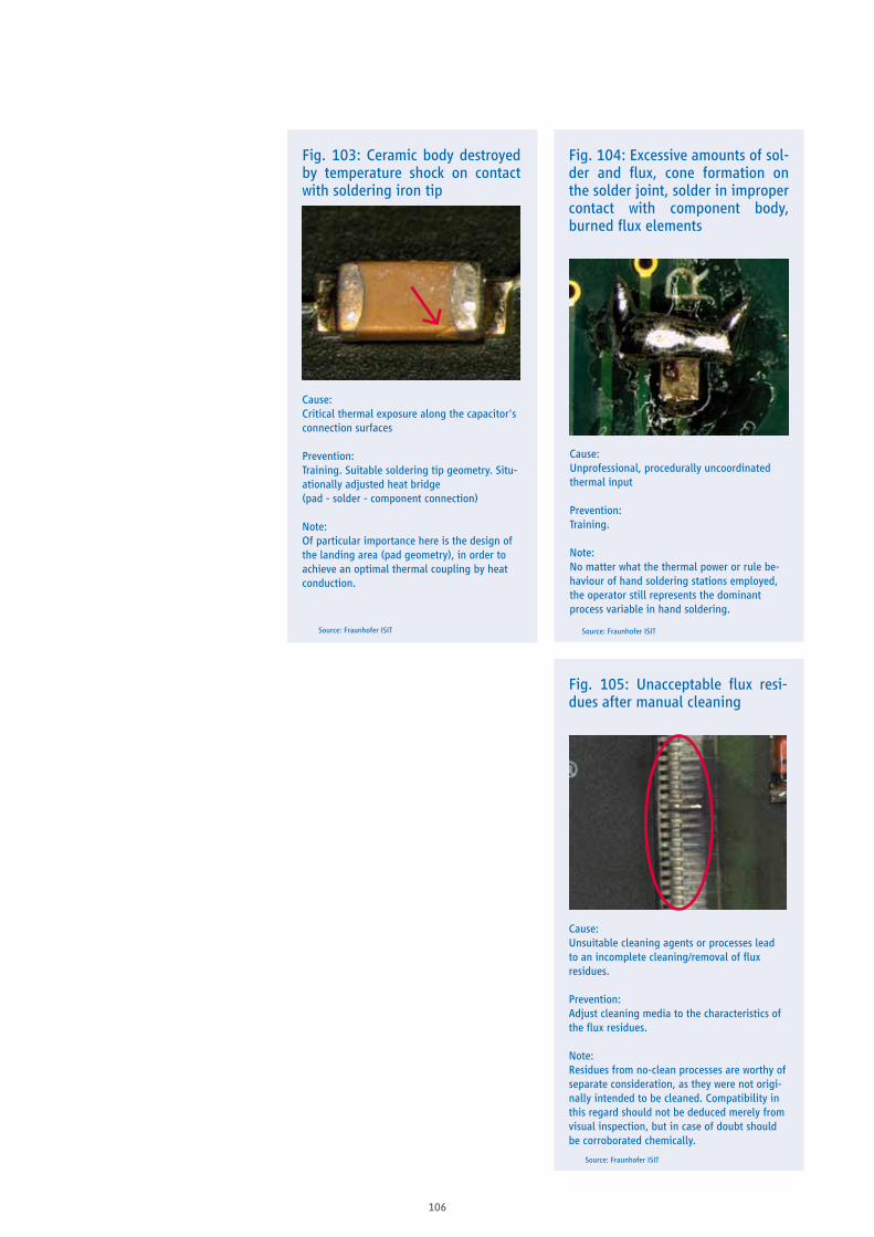
106
Source: Fraunhofer ISIT
Fig. 103: Ceramic body destroyed by temperature shock on contact with soldering iron tip
Fig. 104: Excessive amounts of sol-der and flux, cone formation on the solder joint, solder in improper contact with component body, burned flux elements
Source: Fraunhofer ISIT
Cause:Unprofessional, procedurally uncoordinated thermal input
Prevention:Training.
Note:No matter what the thermal power or rule be-haviour of hand soldering stations employed, the operator still represents the dominant process variable in hand soldering.
Cause:Critical thermal exposure along the capacitor's connection surfaces
Prevention:Training. Suitable soldering tip geometry. Situ-ationally adjusted heat bridge (pad - solder - component connection)
Note:Of particular importance here is the design of the landing area (pad geometry), in order to achieve an optimal thermal coupling by heat conduction.
Source: Fraunhofer ISIT
Fig. 105: Unacceptable flux resi-dues after manual cleaning
Cause:Unsuitable cleaning agents or processes lead to an incomplete cleaning/removal of flux residues.
Prevention:Adjust cleaning media to the characteristics of the flux residues.
Note:Residues from no-clean processes are worthy of separate consideration, as they were not origi-nally intended to be cleaned. Compatibility in this regard should not be deduced merely from visual inspection, but in case of doubt should be corroborated chemically.

107
Fig. 106: Coplanarity
Source: Fraunhofer ISIT
Soldering with rework systems / Defect - Causes - PreventionIn contrast to hand soldering processes, primary factor is the operator (besides the basic device power parameters) modern rework systems are generally aimed toward operator-independent output scatter.
The stated process goal is primarily the correct, sequence-compliant operation and prudent thermal profiling as a function of the component(s) in need of rework.
While some defect patterns can appear in the domain of rework systems and manual soldering, most aspects of defect causes and prevention do diverge.
Defect type: Coplanarity
Cause:Following mechanical deformation (e.g. on QFP connections) or inconsistent heat input, the result may be local deformities, twisting or warping of most large-surface compo-nents and their connection geometries.
A result (and unacceptably wide) gap between component and circuit board (e.g.: with BGA, BTC, etc.) or between component connection and landing area is recognis-able.
During the soldering process, this gap might not be closed, or will be insufficiently closed, by liquid solder; open or defective solder joints can impact the result.
This phenomenon can occur in rework as well as in the inline process itself. Large components, in particular (e.g. BGA sockets, long connector strips), are most susceptible.
Prevention:Avoid inconsistent heat input, for example by using nozzles customised for the compo-nent or a sufficient amount of bottom side heating for profiling.
When designing profiles, it is important to pay attention to the component's colour (e.g.: brightness, reflective surfaces), par-ticularly in primarily radiation-based sys-tems.
The effect is reduced by implementing local, close interval temperature measurement on critical components and by physically sup-porting the circuit board during the rework process.
With very delicate connection geometries, it may be necessary to by-pass mounting the component from the typical component pick position, and instead (if possible) process it directly out of the manufacturer's packag-ing (tray, etc.).
Vacuum pipettes or axis-guided nozzles are preferred in lieu of tweezers or other (clamping) tools.

108
Fig. 107: Bowing
Source: Fraunhofer ISIT
Defect type: Twisting/Bowing
Cause:In general, a distinction must be made between two assembly states:
1. The assembly/circuit board is already bowed or warped prior to reworking.
2. The assembly does not experience tor-sion/bowing until reworking.
The conditions in Category 1 do not lend themselves to correction by rework, as the causes for this lie either in a preceding sol-dering process or in the condition in wich the circuit boards were delivered.
Regarding 1: Under solder heat bombard-ment, the firmly bonded circuit board mate-rials become heated (often considerably) above T
G, disrupting the (initially stable)
PCB geometry by unbalancing the prevail-ing internal stresses in the materials. The release of previously contained internal stresses represents the dominant factor in the type and form of the resulting torsion or bowing.
The causes of the internal stresses them-selves may stem from sub-optimal materials combinations, asymmetric design, incorrect thermal process control, insufficient sup-port effect (centre support), etc.
Regarding 2: Primarily heavy, large-format assemblies require sufficient support, such that during the soldering process the dis-tributed load of the populated assembly does not cause sagging. A sag could even become "frozen" after rework is finished (with regard to the stresses in the solder joints or within the circuit board itself).
In addition to deformations resulting solely from the assembly's own weight, a common cause of pronounced torsion and bowing is the state of clamping forces and tension within the assembly receptacle (especially for relatively thin circuit board substrates).
In this situation, the assembly is held firmly in the x-y direction (at room temperature) by the rework system's clamping frame or holding apparatus. When heated it becomes pressed (particularly clearly at T > T
G)
against the immovable clamping points; the circuit board must either move the holding apparatus, or else it will not withstand the thermally induced stresses at the clamping points and thus yield to the load by twisting or bowing:
Prevention:Regarding 1: Not within the scope of this manual.
Regarding 2: Application of board cen-tre support devices, non-rigid framing or clamping devices; and if possible, use of guided circuit board receptacles and not only of gravity-assisted solutions.

109
Defect type: Popcorning
Cause:Almost all plastics used inside component housings are hygroscopic. Depending on hygroscopic behaviour the result is a more or less pronounced accumulation of water (absorbed mostly in the form of water vapour from the environment) in the com-ponent's interior.
The affinity of this water molecule trans-port in any given component is accounted for mostly indirectly with the MSL (moisture sensitivity level).
When exposed to solder heat, the mois-ture trapped in the component is unable to escape without causing damage. Should the vapour pressure of the trapped water clus-ter (water nest) rise above a certain level, the result is either an "unspectacular" (i.e. invisible from the outside) release along a path of least resistance or a bloating of the casing due to the enormous pressure inside. The latter effect is often known as popcorn-ing.
It is especially tricky to diagnose the extent of popcorning, since these events are fre-quently not pronounced on the surface, yet cause massive damage (for instance, bond tears) to the component internally.
Prevention:Bear in mind the necessity of re-drying moisture-sensitive components (MSL label) and populated assemblies in the case of a rework.
It is now prudent to explore exactly which sub-sections of the assembly will undergo a reflow stress.
The re-drying requirement is always deter-mined by the most temperature sensitive component (highest MSL value).
Fig. 108: Bond tearing off (left image) and surface delamination (right image) following popcorning
Source: Texas Instruments

110
Defect type: Loss of solderability
Cause:During the removal of solder residue the affected landing surfaces suffer undesirably high erosion into the interface of the inter-metallic zone.
The coating of solder residue required to maintain solderability is no longer stably present, resulting in the non-wetting or de-wetting of the affected areas.
This most often occurs in connection with a mechanical removal of solder residue, for example as a result of using solder wicks. Here, two main factors have a decisive impact on the result:
1. Affinity of the solder to preferentially wet the hotter (compared to the landing surface), flux-soaked copper braid.
2. User-dependent and highly variable effect due to direct, force-independent mechanical interference from soldering iron to solder wick to landing area.
Prevention:Implement solder removal preferably with force-controlled or so-called force-free sys-tems, for example hot gas vacuum tools.
Use concave tip geometries in place of sol-der wicks (where possible) along with suffi-cient quantities of flux in order to generate the most uniform solder formations possi-ble at stable planarity.
Fig. 109: Loss of solderability due to solder residue removal
Source: Fraunhofer ISIT

111
Fig. 110: Torn (away) pads
Source: Fraunhofer ISIT
Cause:1. During solder residue removal, non-
molten (at least locally) solder joints cause an inadmissibly high application of force to the affected landing areas; coupled with motion of the component or soldering tool, this can result in pad loss - indicates that process control is locally not hot enough.
2. Equally possible is the loss of a landing surface due to severe overheating at clean-up or during the soldering pro-cess - indicates that process control is locally too hot.
Here, it is almost exclusively the interfaces between the copper of the connection sur-face and the circuit board substrate which are affected.
Most affected by this are: small-footprint, not electrically attached landing surfaces (where it must also be said that the circuit board bond strength and peel strength have a significant influence).
Prevention:Strict compliance with thermally calibrated profiles, in order to rule out processes that are either too hot or too cold. Particularly with thermally inhomogeneous circuit board designs must measurements must be taken at all critical points.
In addition to the challenges originating from the circuit board's design, it is also worth considering the particularities of some component types, as large BGAs and BTCs do not experience the same tempera-tures on all of their leads during soldering.
Besides temperature profiling, it is also advisable use a time- or temperature-guided control to run rework system processes such as "lift component", so that components are not moved into the too-cold environment of the assembly, which would damage indi-vidual pads.
Defecttype:Torn(away)pads
112
Cause:During the actual rework process, a ther-mally secured component corridor becomes (mostly locally and briefly) improperly over-loaded.
The parameters of this component-specific acceptable corridor are characterised by maximum allowable temperature and time; even if only one of these limits is exceeded, the process --and the result -- can no longer be considered reliable.
The causes often lie in defect to consider the prevailing thermal requirements of the assembly in context (shadows from other components, surfaces, default profiles for components, etc.); and in the lack of ther-mal profiling at critical points.
Most often forgotten when reworking fully populated assemblies are separate, individ-ual reflow fitness tests on all components which will be exposed to heat (for example electrolytic capacitors, transformers, or THT press-in connectors).
Of particular importance is --in addition to unflagging observance of thermal lim-its-- the components' durability in the face of repeated soldering heat stress, i.e. the frequency of the maximum allowed heat bombardment on components. Within the categories of housing classified according to J-STD-020 [3], a reflow solder heat stress resistance is assumed to be guaranteed for three passes.
Prevention:Holistic consideration of the assembly area exposed to soldering heat, in particular of the neighbouring components which have no identified level of reflow fitness.
Observance of allowable thermal compo-nent limits both on components directly under rework as well as on components at some remove from the rework.
In the case of repeated solder heat exposure (particularly on thermal overlaps), the num-ber of repetitions should be checked.
Defect type: Thermal overload to component
Fig. 111: Thermally overloaded component
Source: Fraunhofer ISIT

113
Cause:During rework (depending on the assembly- and component-specific thermal require-ments), the assembly (and therefore neces-sarily the circuit board as well) is locally not only heated inconsistently but may also be exposed to repeated solder heat stresses.
Depending on design, process control, rework position and rework frequency, dam-age to the circuit board may result. Besides superficial obvious damage, the circuit board may also be damaged internally.
Particularly in areas of thermal overlap, overloads to the circuit board can occur due to repeated heat stresses as a result of mul-tiple exposures to soldering heat; necessary multiple heat stress durability specifications should be requested individually from the circuit board manufacturer.
Prevention:1. Rework systems: Strict observance of
defined/calibrated profiles at the respec-tive reworking points.
2. Circuit board specifications: Prior to rework, one should check the allowable number of rework steps explicitly speci-fied by the manufacturer.
3. Design: If there is assumed to be an increased probability of rework on an assembly, the choice of materials in such a circuit board should be consid-ered separately (see section 2.7).
Defect type: Thermal overload to circuit board
Fig. 112: Thermally overloaded component
Source: Fraunhofer ISIT

114
Cause:During reworking, temperature-sensitive housings (with often unspecified solder temperature and time boundaries) are exposed to inadmissibly high heat input, thermally overloading the housings.
Causes in the case of rework systems are often related to the method of thermal input. Particularly vulnerable are neigh-bouring areas/housings which are not in fact the focus of rework, but whose positions relative to the heat input (beam path or flow direction) are unfavourable.
For example, if not given proper consid-eration, tall black plastic housings in the immediate area of the component under rework are particularly endangered by the use of radiation-based rework systems.
An very specific danger exists in cases of uncontrolled solder heat exposure to areas containing press-in components; this is due to the fact that while their housings may not take any visible damage, the associ-ated bonded connection zones may become damaged.
Prevention:Observance of each component's and neigh-bouring component's resistance to solder-ing heat; compatibility checks for connec-tion technologies (soldering and press-in techniques). Visual checks are not always enough to verify intactness.
Adequate shielding plates, screens or heat conducting devices can reduce unwanted local collateral heat exposure; for border-line temperature-time limits, evidence should be provided by means of tempera-ture profiling.
Particularly for nearby press-in connections on heavy assemblies, a ban on rework with rework systems altogether can be the result, if the acceptable temperature-time corri-dors are exceeded.
Defect type: Thermal overloadHousing&push-onconnector(s)
Fig. 113: Thermal overload to housing & push-on connectors
Source: Fraunhofer ISIT
115
Cause:During rework, either too much flux is applied or it is applied in the wrong places; often this cause leads to uncertainty over the effectiveness or capacity of flux systems. The consequence can be residues that fail to meet requirements for visual or technologi-cal characteristics.
If attempts are made to clean these flux residues with improper cleaning processes or substances, a "cocktail" of reaction prod-ucts and cleaning substances may develop that is no longer easy to classify.
During re-melting of the soldering paste and dynamic leakage of process gases from solder joints, solder spatters or particles in the region of the component under rework may occur.
Purely manual cleaning always requires particular consideration that cleaning may displace residues loosened in situ into other places in the assembly.
Prevention:Observe classification and compatibility of flux systems with cleaning media and clean-ing processes.
These considerations must be made into account prior to rework, since no flux mate-rial necessarily has the perfect cleaner; fur-thermore, cleaning options for the assem-bly in its fully populated state should be reviewed.
Possible particle displacements or emergent reaction products from an unauthorised cleaning process should be individually checked for type and possible hazard to the assembly (form, fit and function); their innocuousness must be checked in cases of doubt.
Defect type: Inadmissible residues (particulate,flux,unsuitablecleaningprocess/cleaningchemicalsetc.)
Fig. 114: Residues from rework
Source: Fraunhofer ISIT

116
Cause:In the flat array of balls and their associated landing surfaces, a sufficiently even heating condition is not achieved during rework.
Here the primary risk does not involve exceeding the acceptable component tem-perature, but rather a thermal inhomogene-ity in the region of all connections or circuit board landing surfaces; as a result of this, incompletely re-melted areas often emerge in the transition between soldering paste and ball.
Prevention:Observe thermal requirements of the cir-cuit board and component; observe thermal fluctuations resulting from process-depend-ent variance in heat transfer.
This variance can be triggered by the use or non-use of soldering paste or by coplanar-ity effects.
Make control measurements with tempera-ture sensors, and retain associated process parameters by means of individualised sol-dering programs.
Define solder programs on the basis of descriptions of component position and sol-dering mode (soldering on / de-soldering, with or without soldering paste, partially or fully populated assembly, etc.), which can be clearly categorised.
Defect type: Inconsistent heatdistribution(BGAsolder)
Fig. 115: Result of uneven heat exposure
Source: Fraunhofer ISIT
117
5.2.1 Conditions for the emer-gence of electrochemical migrationThe essential factor in the growth of elec-trochemical bridges is the presence of moisture, because it facilitates corrosion. Moisture can build up on the assembly in a number of ways, first as a moisture film adsorbed on the surface, and secondly as condensation.
The critical air humidity level necessary for adsorbed moisture films is strongly depend-ent on the surface energy and surface polar-ity, i.e. on the material, particularly on the solder resist mask and its degree of filling. This is why adsorption can occur even at air humidity levels significantly below the dew point, that is, the temperature difference at which water drops begin to form on the sur-face. Film thicknesses of a few monolayers are sufficient to induce corrosion.
In addition to adsorbed moisture films, condensation induced by temperature cycling can also lead to electrochemical migration. As opposed to moisture films, condensation collects on the spots with higher thermal mass, such as metallised
areas or hygroscopic points, like impu-rities. Organic acids or halide salts, as typical solder resides can often pull the local condensation point down as far as 60 percent of the relative humidity.
Another important factor is the raw material used. Layer counts sufficient for moisture films form for example on metals or metal oxide surfaces beginning at a critical humidity of 60 to 70 percent RH (relative humidity), or on quartz-filled solder resist masks. Corro-sive gases such as nitrogen compounds, H
2S
and CO2 have similar effects and also dis-
solve in moisture films. This is attained only at or above 90 percent RH on aluminium oxide ceramics or unfilled non-polar solder resist masks. At constant climate, humid-ity adsorbs on Sn-metallised epoxide resin substrate, that is, on circuit carriers, pref-erentially on synthetic resin surfaces. It is adsorbed and retained until partial pressure equilibrium is reached.
Furthermore, there must be present a metallisation or solder material which makes electrochemical migration possible in the first place. This means that the mate-
5.2 ElectrochemicalMigration(ECM)
Fig. 116: Corrosion behaviour of Sn
Source: Zestron

118
rial must exhibit an active range in alkaline electrolytes (see grey areas in Figure 116). In distilled water, for example, silver, cop-per, lead, tin and cadmium will migrate well. The bridging propensity varies notice-ably with the potentials of the electromotive series and the narrowing of the material's passive behaviour in the alkaline range. With nickel, for example, migration or cor-rosion does not occur under conditions of condensed water. The susceptibility of an component to electrochemical migration can be estimated with the aid of pH-poten-tial, or so-called Pourbaix diagrams.
In addition to moisture and material, resi-dues and impurities on assemblies have a considerable effect on the emergence of electrochemical migration. Condensation is most favoured when hygroscopic flux residues, dust or salt crystals are present on surfaces, acting as condensation points or condensation seeds for humidity and cor-rosive gases. Adsorption potential is further increased when such surface impurities act as moisture reservoirs, so that the otherwise rapid re-drying of polymers, for example, is only guaranteed at below 30% RH.
5.2.2 Mechanism behind formationAs a result of the moisture film adsorbed on the assembly surface, there is a reduction in surface resistance and thus in the neces-sary insulating capacity of the solder resist masks or circuit carriers. Beyond a critical film thickness the intrinsic conductivity of the adsorbed water film enables the protoly-sis of pure water. This leads to a strong local alkalinisation of the anode, i.e. of the volt-age supply (VCC) or signal leads. Because the pH level has been increased, silver, cop-per, tin and lead in particular (currently the most commonly used elements in metallisa-tion) are polarised in an electrochemically active range.
The anode surface will dissolve in propor-tion to the protolysis flow between contact and ground. Propagation or dendrite growth overwhelmingly follows the direction of the concentration gradient (see Fig. 117).
Fig. 117: Concentration-dependent dendrite growth
Source: Zestron
119
The actual bridging takes place either through galvanic deposition, proceeding from the cathode (GND); or less commonly through the transition of hydroxides/com-plexes to salts, the so-called staining from the anode (VCC or signal contact).
At higher ion concentrations or gradients, smoother growth structures are favoured. Bands or fibre bundles form (Figure 118).
5.2.3 Consequences of electro-chemical migrationIt is often very difficult or impossible to prove that electrochemical migration (ECM) is the cause of damage or defect. When small dendrites appear over short condensation times of typically a few minutes, these are not conductive and burn off immediately. Even so, resultant short-term malfunctions lead to dissatisfaction on the part of the end user and thus to loss of reputation, and depending on application, to high second-ary costs from the defect. In order establish electrochemical migration as the problem, the affected circuits must be recalled from the field and checked for evidence of ECM with scanning electron microscopy. Logis-tical considerations alone often make this impossible. As a result, these defects are thus mistakenly interpreted along with soft-ware glitches and current leakage effects as vague "malfunctions".
When stable dendrites --having current car-rying capacity-- form, temperatures of 600 °C (1110 °F) and higher can occur (Figure 119).
If the circuit does not have a suitable pro-tection or cut-out, these temperatures can start fires. But since this destroys the circuit, one can often only speculate as to whether the cause had been electrochemical migra-tion or electrical breakdown, for example.
The three most important factors behind the emergence and extent of electrochemical migration are moisture risk, degree of impu-rity, and electrical design of the assembly. As such, the user / operator cannot change or control all the relevant factors. Because of the complexity of the mechanism, estimat-ing risk on a case-by-case basis is difficult. A coating will not prevent electrochemical migration in every case. However, integrat-ing a cleaning process prior to coating is a prudent and reliable preventative measure.
Fig. 118: Growth formation as a function of ion concentration.
Source: Zestron
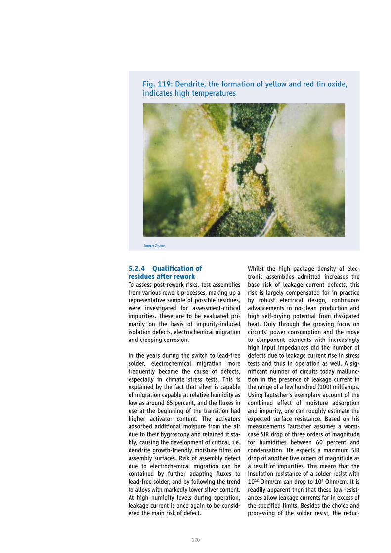
120
5.2.4 Qualificationof residues after reworkTo assess post-rework risks, test assemblies from various rework processes, making up a representative sample of possible residues, were investigated for assessment-critical impurities. These are to be evaluated pri-marily on the basis of impurity-induced isolation defects, electrochemical migration and creeping corrosion.
In the years during the switch to lead-free solder, electrochemical migration more frequently became the cause of defects, especially in climate stress tests. This is explained by the fact that silver is capable of migration capable at relative humidity as low as around 65 percent, and the fluxes in use at the beginning of the transition had higher activator content. The activators adsorbed additional moisture from the air due to their hygroscopy and retained it sta-bly, causing the development of critical, i.e. dendrite growth-friendly moisture films on assembly surfaces. Risk of assembly defect due to electrochemical migration can be contained by further adapting fluxes to lead-free solder, and by following the trend to alloys with markedly lower silver content. At high humidity levels during operation, leakage current is once again to be consid-ered the main risk of defect.
Whilst the high package density of elec-tronic assemblies admitted increases the base risk of leakage current defects, this risk is largely compensated for in practice by robust electrical design, continuous advancements in no-clean production and high self-drying potential from dissipated heat. Only through the growing focus on circuits' power consumption and the move to component elements with increasingly high input impedances did the number of defects due to leakage current rise in stress tests and thus in operation as well. A sig-nificant number of circuits today malfunc-tion in the presence of leakage current in the range of a few hundred (100) milliamps. Using Tautscher's exemplary account of the combined effect of moisture adsorption and impurity, one can roughly estimate the expected surface resistance. Based on his measurements Tautscher assumes a worst-case SIR drop of three orders of magnitude for humidities between 60 percent and condensation. He expects a maximum SIR drop of another five orders of magnitude as a result of impurities. This means that the insulation resistance of a solder resist with 1012 Ohm/cm can drop to 104 Ohm/cm. It is readily apparent then that these low resist-ances allow leakage currents far in excess of the specified limits. Besides the choice and processing of the solder resist, the reduc-
Fig. 119: Dendrite, the formation of yellow and red tin oxide, indicates high temperatures
Source: Zestron

121
tion and monitoring of impurities on the assembly is therefore a key point in prevent-ing defects due to current leakage.
Corrosion creep is also increasingly deserv-ing of mention in connection with halide residues. Copper in particular likes react-ing with chlorides and bromides, which (among other ways) get onto component surfaces through flux. Copper on various metallisations in the assembly should ordi-narily not be exposed to the environment. It should be covered with tin (for example) on solder contacts and by the solder resist mask on circuit paths. In practice there are always discrepancies from process errors or insufficient component specifications, which in the presence of increased environ-mental humidity can lead to copper corro-sion. Here, low-impedance leakage current bridges develop, which can stretch up to several centimetres.
Because a great range of fluxes and pastes is utilised throughout the rework process, as in standard production, the real risk from resi-dues can't be predicted from data sheets. Of course, a low activation level (L), as well as minimal halide content (0), is more favour-able than (H1)-activated. However, with designations one should pay careful atten-tion to the standard used since, with respect to the acceptable halide content at L0 the DIN EN and ANSI J-STD, standards can dif-fer by up to a factor of five (Table 4). Also, and especially with ROL0, pastes can split off hygroscopic short chain multi-carboxylic acids from the resin, as research from Den-mark Technical University (DTU) has shown. While this is good for soldering behaviour, it also creates the risk of critical residues.
When deciding whether or not critical resi-dues are present, it is recommended to fol-low the standards. The most well-known parameter, the so-called ion equivalent, can be found in Chapter 8 of J-STD-001 [8]. Here a threshold of 1.56 µg/cm² is indi-cated for ROL0 and ROL1. However, this value hasn't been updated since the 1970s. For this reason it is advisable to follow the recommendation in the J-STD-001 [8] and work with the manufacturer and user to set
a threshold. That determination should be justified on the basis of history or tests. The IPC-9202 [34] gives the baseline specifica-tions for carrying out such tests, and also defines the methods for determining the ionic residues. Limit values and orientation are provided in the table in IPC-CH65 [3], which also quantifies the amount of allow-able organic acids. The provision for organic acids also allows for an improved risk analy-sis. Should primarily water-soluble acids be found here --and also exhibit a large hygro-scopic potential-- the risk of leakage current should be checked. Location-specific colour tests can determine whether acids are form-ing bridge-building structures between sen-sitive signal inputs or on contacts with high voltage differences (e.g. between ground and voltage supply). Analogue colour tests are also available for visualising halide dis-tributions. Potentially critical points identi-fied in this way can now be stressed using local moisture strain, and circuit function under stress can be checked.
When assessing operational safety after the rework process, another consideration is that there may be other factors besides flux residues. Among other factors, the sig-nificance of imported impurities grows with components and other outsourced parts, with outgassing from polymer materials under solder heat as well as with the human factor in handling and logistics. Therefore, appropriate supply chain management is important to the rework process.
In the creation of this manual, research was limited to the contaminating effects of flux on un-cleaned assemblies. Twelve dif-ferent residue combinations from primary and rework processes were surveyed by means of ion equivalent and flux test, and visually examined in accordance with IPC-A-610 [24]. For un-cleaned test assemblies the ion equivalent scattered between 0.58 and 1.67 µg/cm². The flux test corroborated that there were free carboxylic acids on all test assemblies. With regard to the in-circuit testability and the resin residues on test points, the results varied between accept-able and unacceptable. This can be traced back to a surplus of resins from rework. If a

122
cleaning process is used, flux contamination and other residues from handling and sup-ply chain can be eliminated.
The investigation carried out here is intended to be, and indeed can only be treated as a rough introduction to assessing risk potential. In individual cases it is rec-ommended to carry out the audit in accord-ance with the above-mentioned standards. Because manual cleaning steps are often employed in rework, their results as well should be checked on the basis of the stand-ards mentioned; and these manual cleaning procedures should be monitored and taught analogously to manual soldering processes.
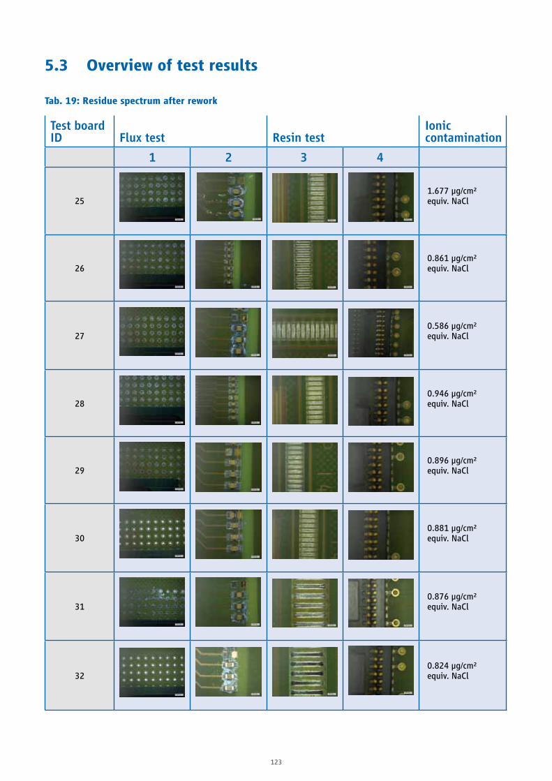
123
Test boardID Flux test Resin test
Ionic contamination
1 2 3 4
251.677 µg/cm² equiv. NaCl
260.861 µg/cm² equiv. NaCl
270.586 µg/cm² equiv. NaCl
280.946 µg/cm² equiv. NaCl
290.896 µg/cm² equiv. NaCl
300.881 µg/cm² equiv. NaCl
310.876 µg/cm² equiv. NaCl
320.824 µg/cm² equiv. NaCl
5.3 Overview of test results
Tab. 19: Residue spectrum after rework
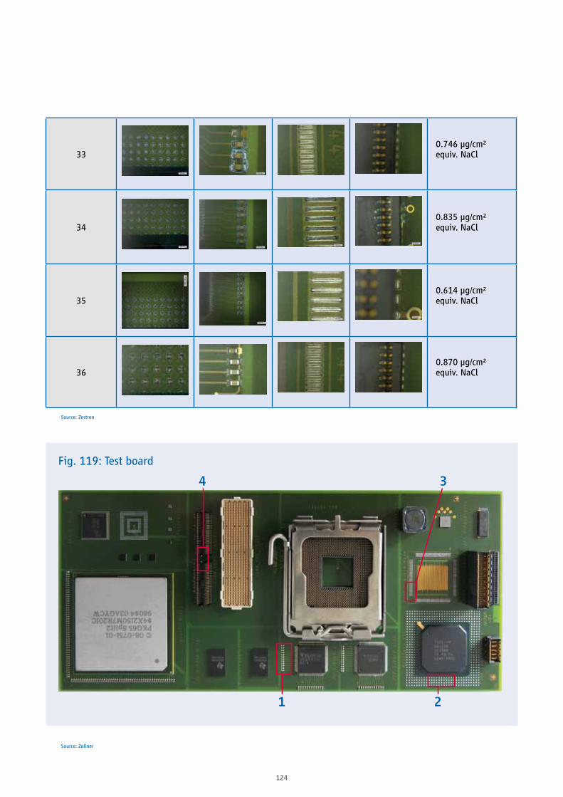
124
330.746 µg/cm² equiv. NaCl
340.835 µg/cm² equiv. NaCl
350.614 µg/cm² equiv. NaCl
360.870 µg/cm² equiv. NaCl
Fig. 119: Test board
Source: Zollner
Source: Zestron
1 2
34

125
Label Flux test Resin testIonic contamination
1 2 3 4
31Prior to cleaning
0.876 µg/cm² equiv. NaCl
32After
cleaning
0.128 µg/cm²equiv. NaCl
Tab. 20: Effect of cleaning
Cleaning parameters: 50 °C (122 °F) / 20 min / ultrasound
Cleaning medium: Zestron FA+
Rinsing parameters:De-ionised water / RT / 10 min. / ultrasound De-ionised water / RT / 10 min. / flow-around
Drying parameters:60°C (140 °F) / 20 min.
Source: Zestron

126
In the following, the core discipline of criticality analysis (thermal process-ing) will be summarised, bearing in mind the product quality (reliability) in a rework context.
This comprehensive weighing of multi-ple factors will allow us to identify (and if needed, to implement) which rework pro-cesses ensure a reliable operating condition even in later assembly applications.
The results gained from visual inspection and cross-sectional analysis show in princi-ple that after a carefully controlled rework, no adverse effect to the reliability of the solder joints or assembly can be expected.
In addition to the present results, the issue of possible solder junction embrittlement (initiated by growth of intermetallic phases) should be considered for more rigid solder joints possessing a relatively small solder gap (e.g. ceramic chip components).
The increase of intermetallic phases ob-served in cross-section (because of addi-tive solder heat exposure) can certainly be metallurgically calculable and is typically categorisable, but there are occasionally critical assembly configurations for which a separate verification of reliability would seem sensible.
The maximum attainable assembly reliabil-ity is always limited by the respective reli-ability levels of the individual components involved. The cumulative reliability is deci-sively impacted by the circuit board, as this single assembly component must withstand the collective heat of all rework soldering processes (see section 2.7).
In order to be confident in a product-spe-cific statement of reliability with respect to reliability on the assembly level following rework, it is recommended to provide indi-vidual qualification on the assembly level.
Concerning this, the following are essential: • Assembly under consideration,
in its initial condition • Assembly in post-rework condition for
assessment • Environment simulation according to
individual mission profile • Comparative visual and destructive
inspection of initial and post-rework condition
• Detailed consideration of all areas exposed to solder heat
• Documentation and conformity assess-ment in accordance with agreed-upon specification(s).
• Release/rejection of product-specific rework process
6 Conclusion/Outlook
6.1 Reliability

127
6.2 Thermal processes6.2.1 Rework / Component-pro-cess preference tableIn the context of the investigations con-ducted, certain rework configurations proved to be particularly suitable. The knowledge gained of component-specific properties, heat transmission methods and advisable process options is laid out in the table below.
Mandantory recommendations cannot be derived from Table 21 for every applica-tion of the assemblies under consideration. Table 22 contains key process control rec-ommendations for rework of typical com-ponent types, with a focus on component replacement.
The focus is on the exchange of compo-nents. When only reworking single solder joints with a view to correcting too much / too little solder, hand soldering is recom-mended in most cases. However, hand sol-dering is counter-indicated for rework on BTC and BGA component types.
Mount-ing loca-tion
Component form Features
Contact solder-ing
IR sys-tem Hot gas Addtl. steps Reballing
Visual inspection X-Ray
Inductor 2-pole High ther-mal mass
X (T) X X
Pre-heat compo-
nent- X (P)
Res_xxx 2-pole 01005-0402 X X X - - X (P)
Ceramic capaci-tor_xxx
2-pole 01005-0402 X1 X XPre-heat compo-
nent- X (P)
xx-PQFP QFN Pitch 0.5mm X X X
Soldering tip with cavetto
- X (P)
Conn-xxx Connector THT – SMT
Mix - R X
mount heat
shield if required
- X X
BGA-xx Ball Grid Array various pitch - X X - X R
(S) X
Conn-FCI MEG Array Ball Grid
Array - X XModify
placement aid
X R (S) X
BGA socket Socket 775 Ball Grid
Array - X X Pre-heat assembly R R
(S) X
Tab. 21: Component process recommendations, based on test assembly
1 Ceramic capacitors: Contact soldering not recommended due to temperature gradient sensitivity; better to use hot gas device.
X = standard processR = with restrictionsP = process qualificationT = soldering tweezersS = special optics

128
Compo-nent type Features
Supporting documentation
Contact soldering
IRsystem
Hot gas
Additional steps
Visual in-spection
X-RayQ
X-RayX
X-RayC
2-pole (chip-
compo-nent)
01005-0402 J-STD-075 [5] R X X
Expanded employee
qualification, observe
temperature gradient
X - - -
2-pole (chip-
compo-nent)
>0402 J-STD-075 [5]
X/T - Caution
- ceramic cap dan-ger, see Tab. 21
X XObserve
temperature gradient
X - - -
Tantalum capaci-
tors- J-STD-075 [5] X X X
Observe peak temperature /
hold timesX - - -
MELF Vitrous body J-STD-075 [5] H X XObserve
temperature gradient
X - - -
SOT/SO-IC
-J-STD-020 [3] J-STD-033 [4]
X/H T T - X - - -
SOT/SO-IC
Heat dissipa-tion surface
J-STD-020 [3] J-STD-033 [4]
H T T Special nozzle X - - √
GullwingPitch
≤0.65 mmJ-STD-020 [3] J-STD-033 [4]
X T TSoldering tip with
cavettoX - - -
GullwingPitch
≤0.65 mm thermal pad
J-STD-020 [3] J-STD-033 [4]
H T TSoldering tip with
cavettoX - - √
J-lead -J-STD-020 [3] J-STD-033 [4]
X T T - X - - -
BGA, CSPRe-melting
balls, various pitch
J-STD-020 [3] J-STD-033 [4] IPC-7095 [6]
- X X Reballing possibleR
(S)√ √ √
BGA, CGA
Non-remelting connections, various pitch
sizes
J-STD-020 [3] J-STD-033 [4] IPC-7095 [6]
- X/R X
Limited reballing, additional deposit
of soldering paste
necessary
R(S)
√ √ √
DPAK
Heat dissipation/sur-
face thermal pad surface
J-STD-020 [3]J-STD-033 [4]
- T T - X - - √
BTC -J-STD-020 [3]J-STD-033 [4]IPC-7093 [7]
- T T - X/R √ - √
ConnectorIn SMT,
through-hole
J-STD-020 [3]J-STD-033 [4] X X X
Special nozzle, placement aids, pay attention to printed circuit board bowing
X - - -
Connector In SMT, BGAJ-STD-020 [3]J-STD-033 [4] - X/R X/R
Special nozzle, placement aids, pay attention to printed circuit board bowing
X √ (√) √
Tab. 22: Component type process recommendations
X = standard processR = with restrictionsP = process qualificationT = soldering tweezersH = hot gas pen
S = special opticsTP = temperature profile requiredC = client-specificQ = solder junction quality
129
In rework terms, the key technological fac-tors can be attributed either to thermal parameters (component and circuit board level), or else to chemical interactions (with a focus on residue analysis), such as the fol-lowing:• Multiple solder heat stress situations
resulting from thermal overlaps (see sec-tions 2.4 and 4.4)
• MSL (particularly when history of mois-ture exposure is unknown - see sections 2.9 and 5.1)
• Flux compatibility (chemical and thermal - see sections 2.4 and 5.2)
While implementing the above considera-tions during a rework in principle cause extra costs, the underlying limits, correc-tive actions and tolerance ranges are for the most part sufficiently defined.
In rare, product-specific incidents, border-line cases may still occur despite taking account of and compliance with all required parameters (both technologically adequate as well as authorised in the sense of a prior tuned customer-supplier agreement). Such instances must be examined on a case-by-case basis.
In such a case, the clear classification with respect to the controllable as well as fully authorised rework process must, if neces-sary, be checked for assignment to the repairs department.
The deciding factor in whether rework or repair is called for is first to clarify to what extent corrective measures can restore full the item's full conformance with its respec-tive specifications or drawings.
6.2.2 Repair / component processIn accordance with the definitions of rework, modification or repair laid out in section 2.1, it is certainly possible to classify correc-tive measures, but on short notice it is often not possible to gather all the detailed infor-mation for an unambiguous classification.
Here a premature categorisation as rework must be ruled out, because ostensibly minor details must often be considered, whose salience cannot be reduced to thermal parameters alone.The essential criticality does not necessar-ily lie in insufficient technological com-patibility of the corrective procedure, but frequently rather in product conformities which are not 100 percent met.
Key questions on this matter (some of which were already addressed in section 2.1) are recapitulated as a basis for improving risk assessment in terms of deciding between rework and repair.
Do corrective measures merely represent an unscheduled and temporary measure or are they in danger of becoming rou-tine?• As a rule, solder joints from in line sol-
dering processes with acceptable amount of solder produce acceptable assembly properties, inasmuch as the underlying design and class division are consistent.
• Prior to a routine corrective intervention, which gives the solder joints an "extra portion" of solder, it should be warned that the expected gains in reliability or admissibility are not always commensu-rate to the risk and/or effort involved.

130
Doesthemodificationcomewithcaveats(quality,reliability),andifso,howgreatare they?• The answer to this question is can usually
be carried out in consultation with the cli-ent, as the actual implications for product characteristics are generally not possible to ascertain through visual inspection or X-ray diagnosis.
• Special attention must be paid to assem-blies which feature multiple joining tech-nologies; for example, a thermally ideal BGA replacement (see Chapter 2.2) is not perfectly admissible when a press fit con-nector is located nearby.
• Are there other thermal limits besides the actual SMT or THT components which should be considered separately? • Conformal coatings, for example, do
not always respond to excessive heat input with burn effects visible to the naked eye.
• The danger of (often only local) delamination of protective coatings as a result of increased heat input must be checked for separately, as critical microclimates can develop along the interface between component (printed circuit board) and protective coating.
From the customer point of view, is an additional procedure even permitted?• Here, a distinction should first be made,
whether and to what degree corrective measures are permissible and sensible in the first place.
• Often minor corrections with hand sol-dering irons are allowed, while a BGA replacement is considered out of the question.
• A disallowed or incorrectly applied proce-dure (especially with seemingly "simple" component types) can lead to degrada-tion or loss of function. For example, frac-tures in glass diodes can result from use of a soldering iron, while the client would have permitted the use of a hot gas pen.
Are there restrictions with respect to moisture-sensitivecomponents(MSL)?• This theme appears at various places
in this guideline and is discussed with acknowledgement given to the typical MSL representatives.
• The danger to the component or to the assembly increases tremendously once the classical MSL attributions can no longer be applied with confidence (e.g. due to incomplete data sheets), or if standard re-drying recommendations (according to J-STD-020) no longer fit the assembly's development or integration condition of construction.
• The same things that are described and classified purposely for moisture-sensi-tive also applicable in a modified form to some moisture-sensitive circuit board materials, but in these cases an authorita-tive classification is not possible.
In summary, both reworking and repair are suitable measures for guaranteeing or restoring an assembly's integrity where necessary, either as part of the running production process or in the event of delayed corrections.
In addition to basic considerations of capa-bility, the technologies and concepts to be applied in practice continuously require authorisation from the customer: Even minor corrections are not necessarily per-mitted unless they are explicitly defined in advance.
131
7 Closing Remarks
The reworking process is a controllable one, provided it is diligently carried out and all boundary conditions for components, printed circuit board and soldering process as well as handling thereof (as set forth in this guideline) are observed and complied with.
The right rework process can produce quali-tatively consistent and equal products. In addition to a customised thermal profile, a qualified and reproducible rework process sequence are indispensable parameters in achieving this.
The foundation for this - in the sense of fundamentally safe and feasible rework processes - is a suitable choice of printed circuit board material in light of the addi-tional thermal demands represented by the rework process.
Given the use of stable processes and situ-atively customised rework procedures, the same requirements on qualitative execution and product quality apply in rework as in the line process.
Particularly applicable are the same accept-ance and testing accuracy criteria, as well as the rigorous compliance with all secondary aspects with regard to form, fit and func-tion.
Always required is a demand-oriented and calculating review of the essential neces-sity (particularly with respect to kind and extent) of rework steps.
Besides just successful rework procedures, the focus is also on implementing safe pro-cess control as a rework process window.
Purely cosmetically motivated corrections to solder joints are explicitly discouraged.

132
8 Corporate and Research Partners
Fraunhofer Institute for Silicon Technology (Fraunhofer-InstitutfürSiliziumtechnologie)

133
9 Bibliography
[1] IPC, IPC-T-50J. [2] DIN, DIN EN 61760-1 – Surface
mounting technology - Part 1: Stand-ard method for the specification of surface mounting components (SMDs), 2006/10.
[3] J-STD, J-STD-020 Rev E – Moisture/reflow sensitivity classification for non-hermetic surface-mount devices, 2014/12.
[4] J-STD, J-STD-033 Rev C – Standard for handling, packing, shipping, and use of moisture/reflow sensitive surface-mount devices, 2012/02.
[5] J-STD, J-STD-075 – Classification of Non-IC Electronic Components for Assembly Processes, 2008/08.
[6] IPC, IPC-7095 Rev C – Design and Assembly Process Implementation for BGAs, 2013/01.
[7] IPC, IPC-7093 – Design and Assembly Process Implementation for Bottom Termination Components, 2011/03.
[8] J-STD, J-STD-001 Rev E – Requirements for Soldered Electrical and Electronic Assemblies, 2010/04.
[9] DIN, DIN EN 61191-1 through 4 – Electronic structures on circuit boards (German: Elektronikaufbauten auf Leiterplatten) Part 1 through 4, 1 & 2 2014/02; 3 & 4 1999/6.
[10] DIN, DIN EN 61192-5 – Workmanship requirements for soldered electronic assemblies - Part 5: Rework, modifica-tion and repair of soldered electronic assemblies, 2007/12.
[11] DIN, DIN EN 61760-2 – Surface mount-ing technology - Part 2: Transporta-tion and storage conditions of surface mounting devices (SMD), 2007/10.
[12] IPC, IPC-7711/7721 Rev B – Rework, Modification and Repair of Electronic Assemblies, 2007/11.
[13] ECSS, ECSS-Q-ST-70-28 Rev C – Repair and modification of printed circuits board assemblies for space use, 2008/07.
[14] ECSS, ECSS-Q-ST-70-08 Rev C – Man-ual soldering of high-reliability elec-trical connections, 2009/03.
[15] ECSS, ECSS-Q-ST-70-38 Rev C – High-reliability soldering for surface-mount and mixed technology, 2008/07.
[16] IGF, IGF 15.535N – "Reliability and soldering heat resilience of new con-structions in the manual repair process of lead-free electronic assemblies" (German: Lötwärmebeständigkeit und Zuverlässigkeit neuer Konstruktionen im manuellen Reparaturprozess blei-freier elektronischer Baugruppen), 2011/01.
[17] IPC, IPC J-STD-004B, IPC. [18] DIN, DIN EN 61190-1-1, DIN. [19] IPC, IPC-TM650. [20] J-STD, J-STD-004 – Requirements for
Soldering Fluxes. [21] EC Guidelines, EC Guideline 2002/95/
EG (RoHS 1) – Guideline 2002/95/EC for Restriction of Hazardous Sub-stances in Electrical and Electronic Devices (German: Richtlinie 2002/95/EG zur Beschränkung der Verwend-ung bestimmter gefährlicher Stoffe in Elektro- und Elektronikgeräten), 27.01.2003, 2003.
[22] EC Guidelines, EC Guideline 2011/65/EC (RoHS 2) – Guideline 2011/65/EC for Restriction of Hazardous Substances in Electrical and Electronic Devices (Revised Version) (German: Richtlinie 2011/65/EU zur Beschränkung der Verwendung bestimmter gefährlicher Stoffe in Elektro- und Elektronikgeräten (Neufassung)), 08.06.2011, 2011.
[23] WEEE Guidelines, WEEE Guideline 2002/96/EG or subsequent 2012/19/EU on Waste Electrical and Electronic Equipment, 2002/2012.
[24] IPC, IPC-A-610 Rev E – Acceptability of Electronic Assemblies, 2011/04.
[25] Max H. Poech, Fraunhofer Institut für Siliziumtechnologie, ISIT Seminar on Technologies for Temperature Meas-urement – "Temperature Measurement in Reflow" (German: ISIT-Seminar Tem-peraturmesstechnik – Temperaturmes-sung im Reflow), 2013/10.
[26] Regulation on Hazardous Substances, (Appendix II, No. 2.3 Paragraph 7) (German: GefStoffV, GefStoffV Gefahrstoffverordnung (Anhang II Nr 2.3 Abs. 7)).
[27] TRGS [Technical Regulations for Haz-ardous Substances, German Technis-che Regel für Gefahrstoffe], TRGS 420
134
– Procedure- and substance-specific criteria for hazard assessment, (Ver-fahrens- und stoffspezifische Kriterien für die Gefährdungsbeurteilung).
[28] BGI, BGI 790-014 – Soft-soldering with soldering irons (German: Weichlöten mit dem Lötkolben).
[29] TRGS, TRGS 406 – Sensitising agents for airways (German: Sensibilisierende Stoffe für die Atemwege) – Item 5. Par-agraph 2.
[30] TRGS, TRGS 900 – Occupational expo-sure limit values (German: Arbeit-splatzgrenzwerte).
[31] TRGS, TRGS 528. [32] IPC, IPC-7527 DE – Solder Paste
Printing Acceptance Guide (German: Anforderungen an den Lotpastendruck) [English version available], 2012.
[33] AiF-Projekt, "Reliability and soldering heat resilience of new constructions in the manual repair process of lead-free electronic assemblies" (German: Lötwärmebeständigkeit und Zuver-lässigkeit neuer Konstruktionen im manuellen Reparaturprozess bleifreier elektronischer Baugruppen), IGF-Pro-jekt 15535N,“ Fraunhofer Institut für Siliziumtechnologie (ISIT), Itzehoe.
[34] IPC, IPC-9202. [35] IPC, IPC-CH65. [36] J-STD, J-STD-002 – Solderability Tests
for Component Leads, Terminations, Lugs, Terminals and Wires.
[37] J-STD, J-STD-003 – Solderability Tests for Printed Boards.
[38] Government Electronics and Informa-tion Technology Association, GEIA-STD-0015

135
ABBGABall Grid Array - surface-mounted hous-ing with ball-shaped connection points arranged on the underside of the unit in a two-dimensional array.There are typically two variants recognized: either with "low-melting" or "high-melting" balls. After melting during the reflow pro-cess, the low-melting balls change from their original ball form into a barrel shape once the solder deposit is fully integrated. High-melting balls (e.g. of PbSn10) mostly maintain their original form, even after the reflow process, changing unsignificantly as they melt locally in the solder joint area.BTCBottom Termination Components - Compo-nents with bottom connections.
CCAFConductive Anodic Filamentation - Forma-tion of copper filaments in the base mate-rial, growing from the anode to the cathode (effect taking place within the circuit board in the direction of fibre orientation)CleanableA state or quality of flux residue after sol-dering (in accordance with the soldering procedure approved by the flux manufac-turer) generally requiring cleaning, because the residues are (at least under some condi-tions) categorised as corrosive.ConvectionCommonly used method of heat transfer within soldering systems (primarily in so-called reflow full convection soldering sys-tems) as well as rework systems in the form of hot gas variantsConduction(aka thermal conduction) Another com-monly used physical method of heat trans-fer, primarily in hand-held solder devices (solder tip). Also indirectly used transfer heat energy using molten solder.CondensationAnother method of heat transfer in which heat can be transferred relatively quickly and efficiently by depositing latent heat through a state-of-matter transformation (vapour to liquid). In use in soldering sys-tems, favoured in so-called vapour phase soldering systems; however, such systems are not covered in detail in this manual.
DDFNDual Flat No Lead - Component type belong-ing to the BTC family.Daisy chainDaisy Chain is a wiring scheme wich allows to monitore component connections, includ-ing solder joints, via Ohm mesurement.DICYHardening mechanism for circuit board materials (relating to the resin system(s) used)DINGerman Institute for Standardisation (German: Deutsches Institut für Normung)DMADynamic Mechanical Analysis - Measure-ment method for electronically determining modulus of elasticity.
EEutecticDescribes an alloy which at its current eutec-tic percentage ratio of constituents yields the lowest melting point for that alloy; in a eutectic ratio the liquidus line and the soli-dus line meet to a point.The alloy thus no longer has a melting range, but instead only a melting point.ECMElectrochemical Migration - build-up of (conductive) dendrites in the presence of ionic contamination, moisture and differ-ence in potential ENIGElectroless Nickel / Immersion Gold - circuit board surface ECSSEuropean Cooperation for Space Standardi-sationENEuropean Standard (German: Europäische Norm)EIAElectronic Industries Alliance
F
GGullwingDesignation for a type of connector; name based on resemblance to a gull's wing. Common examples of components which use this connector shape include QFP, SOT, etc.
10 Glossary

136
HHeat trensfer - see section 2.12 for addi-tional information
IISTInterconnect Stress Test - accelerated reli-ability test for scoring how resilient plated through holes and PCB interconnects are to repeated thermal cycling. The test uses the self heating of structures of the pcb.IPC/JEDEC J-STD-020 [3]Moisture/reflow sensitivity classification for nonhermetic surface-mount devicesIPCOriginally Institute for Printed Circuit; now Association Connecting Electronic Industries
IPC/JEDEC J-STD-033 [4]Standard for handling, packing, shipping, and use of moisture/reflow sensitive sur-face-mount devicesIECInternational Electrotechnical Commission
JJ-STDRefers to publications from the American organisation Joint Industry StandardJ-STD-001 [8]Requirements for Soldered Electrical and Electronic AssembliesJ-STD-002 [36]Solderability Tests for Component Leads, Terminations, Lugs, Terminals and WiresJ-STD-003 [37]Solderability Tests for Printed BoardsJ-STD-004 [20]Requirements for Soldering FluxesJ-STD-075 [5](EIA/IPC/JEDEC) Classification of Non-IC Electronic Components for Assembly Pro-cessesJEDECSolid State Technology Association (for-merly Joint Electron Device Engineering Council – JEDEC) - American organisation for the standardisation of semiconductors
K
LLGALand Grid Array - component type, belong-ing to the BTC familyLiquidusTemperature under which all elements in an alloy begin to solidify
MModificationOverhaul of a product's operational capacity in order to satisfy new acceptance criteria. Changes are generally necessary in order to reflect design changes present in blueprints, change requests and the like. Changes can be carried out only with express authorisa-tion and detailed description in the relevant documentation changes. ModificationThe modification of a printed circuit assem-bly shall be the revision of interconnecting features by interrupting conductors or add-ing components as well as wire connections (ESA)MicroviaVertical connection hole (usually laser-drilled), executed as a blind hole for electri-cally connecting two directly superimposed layers by means of metallisation.MSLMoisture Sensitivity Level - describes the level of sensitivity of certain water-absorb-ing component types, which must be dried prior to solder heat stress, so as to avoid internal component damage.
NNo cleanThe state or quality of flux residue after soldering (in accordance with the solder-ing procedure approved, by the flux manu-facturer) which generally does not require cleaning, because the residues are not cat-egorised as corrosive.
O
137
PPQFPPlastic Quad Flat Pack(age) - surface-mounted package type with gullwing-style leadsPin in pasteProcessing of component parts for through-hole mounting within a reflow-based pro-duction procedure, in which a customised solder deposit is used with the goal of supplanting the original (and more costly) wave soldering process. Here, the stability of reflow heat on the affected component is crucial.Phenolically hardened Hardening mechanism for circuit board materials (relating to the resin system(s) used)QQFPQuad Flat Pack(age) - surface-mounted package type with gullwing-style leadsQFNQuad Flat No Lead - Component type belonging to the BTC family.
RReballingProcess which serves to exploit other alloy properties (e.g. lead-free or lead- containing) by replacing balls, especially of BGAs, substrates or other component designs; or to restore the original ball matrix.ReworkReworking / refinishing of non-conforming items with original processing or equivalent thereof in order to ensure that the item is fully compliant with its respective blue-prints or specificationsRework (according to European Space Agency-ESA)Process of reworking of a defective solder joint (without changing the component) as a consequence of the repair or modification process or for restoring good workmanship of potentially defective solder jointsRework systemThis designation encompasses all systems and machines whose operation is (at least partially) automated through programming and/or user guidance, and which, compared to a purely manual mode of operation, enable an improved, reproducible pro-cess design. This type of apparatus is also characterized by a distinct component- or assembly-specific thermal profile and an on-demand accessible program.
Repair(ESA)Change of a component with all its associ-ated connections, including the fixing down of a lifted pad or track or any similar proce-dure described in this StandardNOTE 1 Changing of components for tuning, i.e. desoldering and changing component value is not considered a repair, rework or modification operation.NOTE 2 During tuning, solder jointing is achieved with a minimum of solder, just enough to ensure contact.RepairRestoration of a defective item's functional capacity in such a way that does not ensure that the item is fully compliant with its respective blueprints or specifications.RadiationPhysical method of heat transfer in which surface temperature of the radiating body and the surface colour of the receiving body significantly affect heat transfer rate.
SSIRSurface Insulation Resistance - this is a key parameter particularly in the qualification of fluxes or impurities (no clean or clean-able).SolidusTemperature at which all elements in an alloy are solidSAC305Name for one of the most commonly used lead-free soft-solder alloys, composed of tin (Sn), silver (Ag) and copper (Cu). SAC305 is so called for its Sn-Ag-Cu composition of 3.0% Ag and 0.5% Cu, the remainder being tin.SnPb37Eutectic tin-lead solder with 63% Sn and 37% PbSAC solderGeneral term for derivations of the tin-sil-ver-copper (Sn-Ag-Cu) solder formulaSMDSurface Mount DeviceSMTSurface Mount Technology

138
TTHDThrough Hole DeviceTHTThrough Hole TechnologyTGAThermogravimetric Analysis - measure-ment method for determining temperature-dependent mass loss (e.g. of circuit board materials)TMAThermomechanical Analysis - measurement procedure for determining a material's deformation under a defined application of force
UVW
XX-RayBand of the electromagnetic spectrum including waves of 0.1 to 10 nm with energy levels typically in the keV range. Also an established method of non-invasively diag-nosing internal component elements (for instance copper conducting paths) and sol-der joints not amenable to visual inspec-tion (BTC, BGA etc.). A variety of guidelines, standards and practices reference this type of diagnosis.
YZ


ZVEI - German Electrical and ElectronicManufacturers’ AssociationLyoner Strasse 960528 Frankfurt am Main, GermanyPhone: +49 69 6302-0Fax: +49 69 6302-317E-mail: [email protected] Titl
e pa
ge p
hoto
cre
dit:
Ast
rid
Gas
t, G
oodl
uz, V
RD /
Foto
lia.c
om //
Leo
ni