Embed Size (px)
Citation preview
1
1
Hardware Design I Chap. 5Memory elements
Computing Architecture Lab.Hajime Shimada
E-mail: [email protected]
Hardware Design I (Chap. 5) 2Computing Architecture Lab.
Hajime Shimada
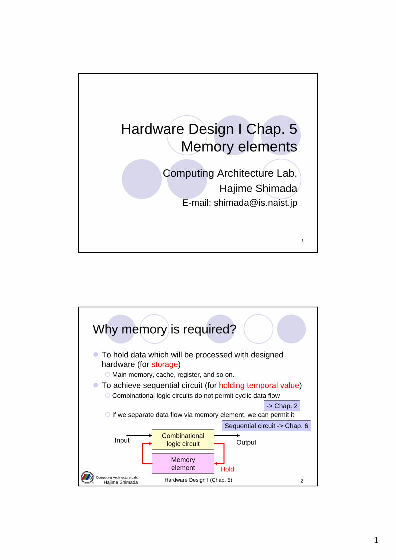
Why memory is required?
To hold data which will be processed with designed hardware (for storage)
Main memory, cache, register, and so on.
To achieve sequential circuit (for holding temporal value)Combinational logic circuits do not permit cyclic data flow
If we separate data flow via memory element, we can permit it
Combinationallogic circuit
Memoryelement
Input Output
Hold
-> Chap. 2
Sequential circuit -> Chap. 6

2
Hardware Design I (Chap. 5) 3Computing Architecture Lab.
Hajime Shimada
Outline
Flip-flops and latches (for temporal value)SR flip-flop and its variationsD flip-flop and its variationsD latch
Random Access Memory (RAM) and related structure (for storage)
Basic organization of RAMStatic RAM (SRAM)The other RAMsContent Addressable Memory (CAM)
Hardware Design I (Chap. 5) 4Computing Architecture Lab.
Hajime Shimada
What’s flip-flop?
Assume seesawOutputs Q and Q’ take opposite statusQ and Q’ flip under some condition
There are several types of flip-flopsSR flip-flopClocked SR flip-flopMaster-slave SR flip-flopMaster-slave D flip-flopEdge trigger D flip-flop
0
0
1
1
Q’
Q’
Q
Q

3
Hardware Design I (Chap. 5) 5Computing Architecture Lab.
Hajime Shimada
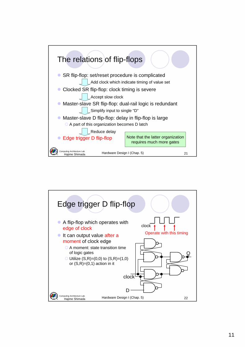
The relations of flip-flops
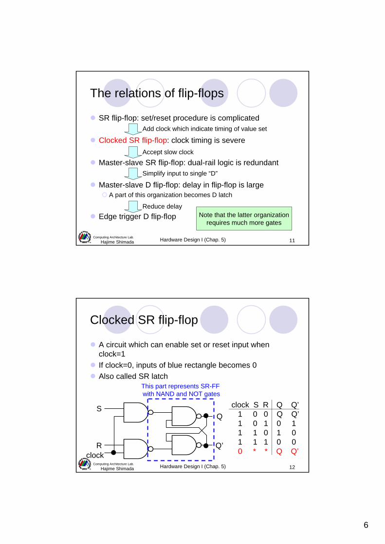
SR flip-flop: set/reset procedure is complicated
Clocked SR flip-flop: clock timing is severe
Master-slave SR flip-flop: dual-rail logic is redundant
Master-slave D flip-flop: delay in flip-flop is largeA part of this organization becomes D latch
Edge trigger D flip-flop
Add clock which indicate timing of value set
Accept slow clock
Simplify input to single “D”
Reduce delayNote that the latter organization
requires much more gates
Hardware Design I (Chap. 5) 6Computing Architecture Lab.
Hajime Shimada
SR flip-flop
Set Reset flip-flop (SR-FF)“Set” means “output 1”“Reset” means “output 0”
e.g. reset statusThe feedback loop creates stable status
S R Q Q’0 0 Q Q’ (Memorize)0 1 0 11 0 1 01 1 0 0 (Prohibit)
S
R Q
Q’0
1
1
0
0
1
4
Hardware Design I (Chap. 5) 7Computing Architecture Lab.
Hajime Shimada
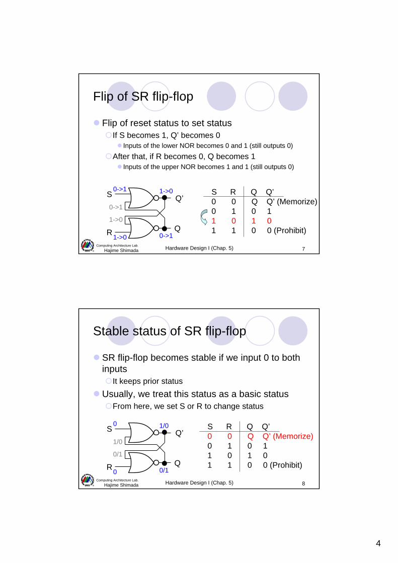
Flip of SR flip-flop
Flip of reset status to set statusIf S becomes 1, Q’ becomes 0
Inputs of the lower NOR becomes 0 and 1 (still outputs 0)
After that, if R becomes 0, Q becomes 1Inputs of the upper NOR becomes 1 and 1 (still outputs 0)
S R Q Q’0 0 Q Q’ (Memorize)0 1 0 11 0 1 01 1 0 0 (Prohibit)
S
R Q
Q’0->1
1->0
1->0
0->1
0->1
1->0
Hardware Design I (Chap. 5) 8Computing Architecture Lab.
Hajime Shimada
Stable status of SR flip-flop
SR flip-flop becomes stable if we input 0 to both inputs
It keeps prior statusUsually, we treat this status as a basic status
From here, we set S or R to change status
S R Q Q’0 0 Q Q’ (Memorize)0 1 0 11 0 1 01 1 0 0 (Prohibit)
S
R Q
Q’0
0
1/0
0/1
1/0
0/1
5
Hardware Design I (Chap. 5) 9Computing Architecture Lab.
Hajime Shimada
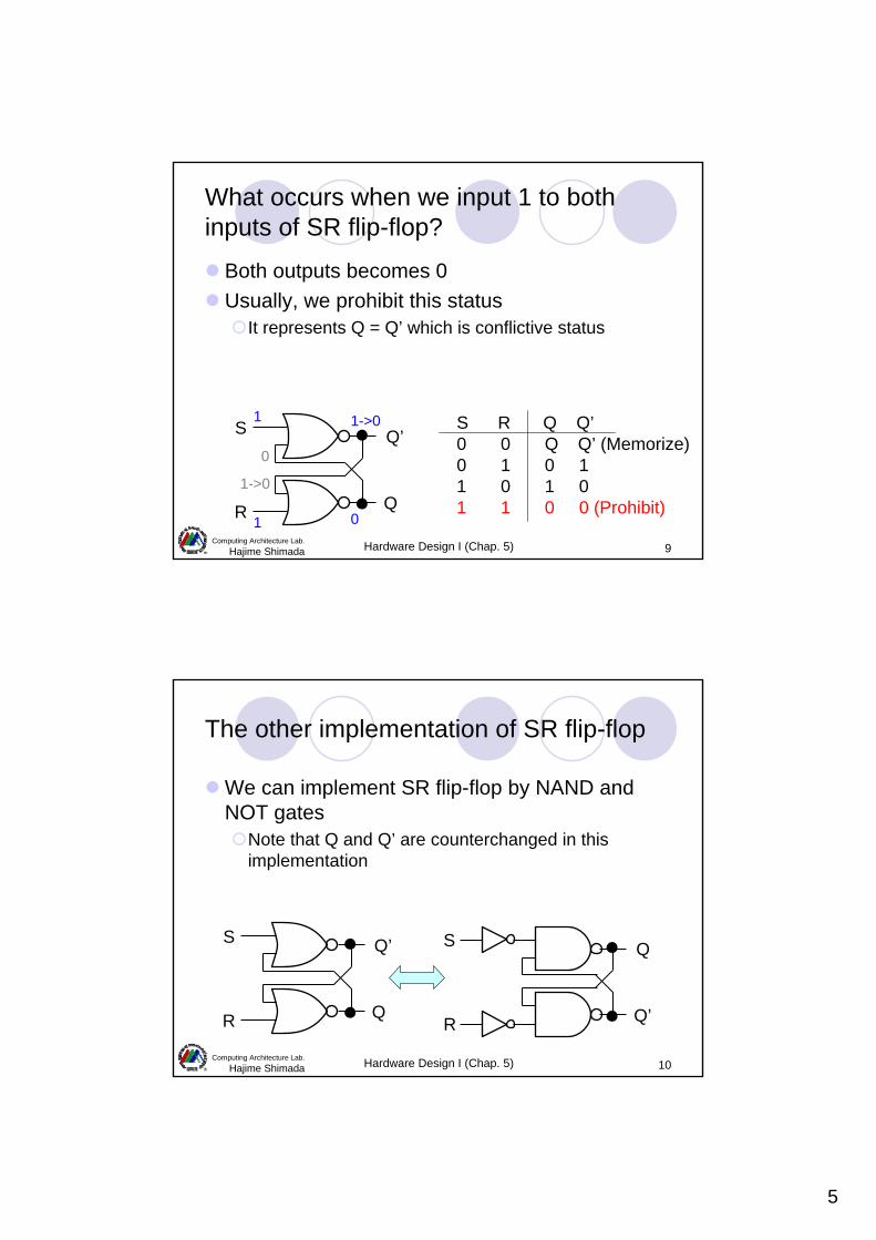
What occurs when we input 1 to both inputs of SR flip-flop?
Both outputs becomes 0Usually, we prohibit this status
It represents Q = Q’ which is conflictive status
S R Q Q’0 0 Q Q’ (Memorize)0 1 0 11 0 1 01 1 0 0 (Prohibit)
S
R Q
Q’1
1
1->0
0
0
1->0
Hardware Design I (Chap. 5) 10Computing Architecture Lab.
Hajime Shimada
The other implementation of SR flip-flop
We can implement SR flip-flop by NAND and NOT gates
Note that Q and Q’ are counterchanged in this implementation
S
R Q
Q’ S
R Q’
Q
6
Hardware Design I (Chap. 5) 11Computing Architecture Lab.
Hajime Shimada
The relations of flip-flops
SR flip-flop: set/reset procedure is complicated
Clocked SR flip-flop: clock timing is severe
Master-slave SR flip-flop: dual-rail logic is redundant
Master-slave D flip-flop: delay in flip-flop is largeA part of this organization becomes D latch
Edge trigger D flip-flop
Add clock which indicate timing of value set
Accept slow clock
Simplify input to single “D”
Reduce delayNote that the latter organization
requires much more gates
Hardware Design I (Chap. 5) 12Computing Architecture Lab.
Hajime Shimada
Clocked SR flip-flop
A circuit which can enable set or reset input when clock=1If clock=0, inputs of blue rectangle becomes 0Also called SR latch
Q’
QS
Rclock
clock S R Q Q’1 0 0 Q Q’1 0 1 0 11 1 0 1 01 1 1 0 00 * * Q Q’
This part represents SR-FF with NAND and NOT gates
7
Hardware Design I (Chap. 5) 13Computing Architecture Lab.
Hajime Shimada
Input
Output
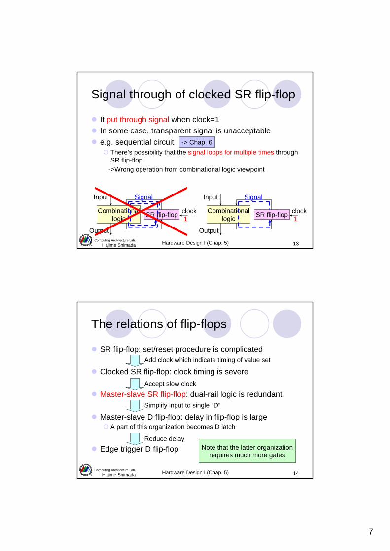
Signal through of clocked SR flip-flop
It put through signal when clock=1In some case, transparent signal is unacceptablee.g. sequential circuit
There’s possibility that the signal loops for multiple times through SR flip-flop
->Wrong operation from combinational logic viewpoint
Combinationallogic SR flip-flop clock
Signal
1
Input
Output
Combinationallogic SR flip-flop clock
Signal
1
-> Chap. 6
Hardware Design I (Chap. 5) 14Computing Architecture Lab.
Hajime Shimada
The relations of flip-flops
SR flip-flop: set/reset procedure is complicated
Clocked SR flip-flop: clock timing is severe
Master-slave SR flip-flop: dual-rail logic is redundant
Master-slave D flip-flop: delay in flip-flop is largeA part of this organization becomes D latch
Edge trigger D flip-flop
Add clock which indicate timing of value set
Accept slow clock
Simplify input to single “D”
Reduce delayNote that the latter organization
requires much more gates
8
Hardware Design I (Chap. 5) 15Computing Architecture Lab.
Hajime Shimada
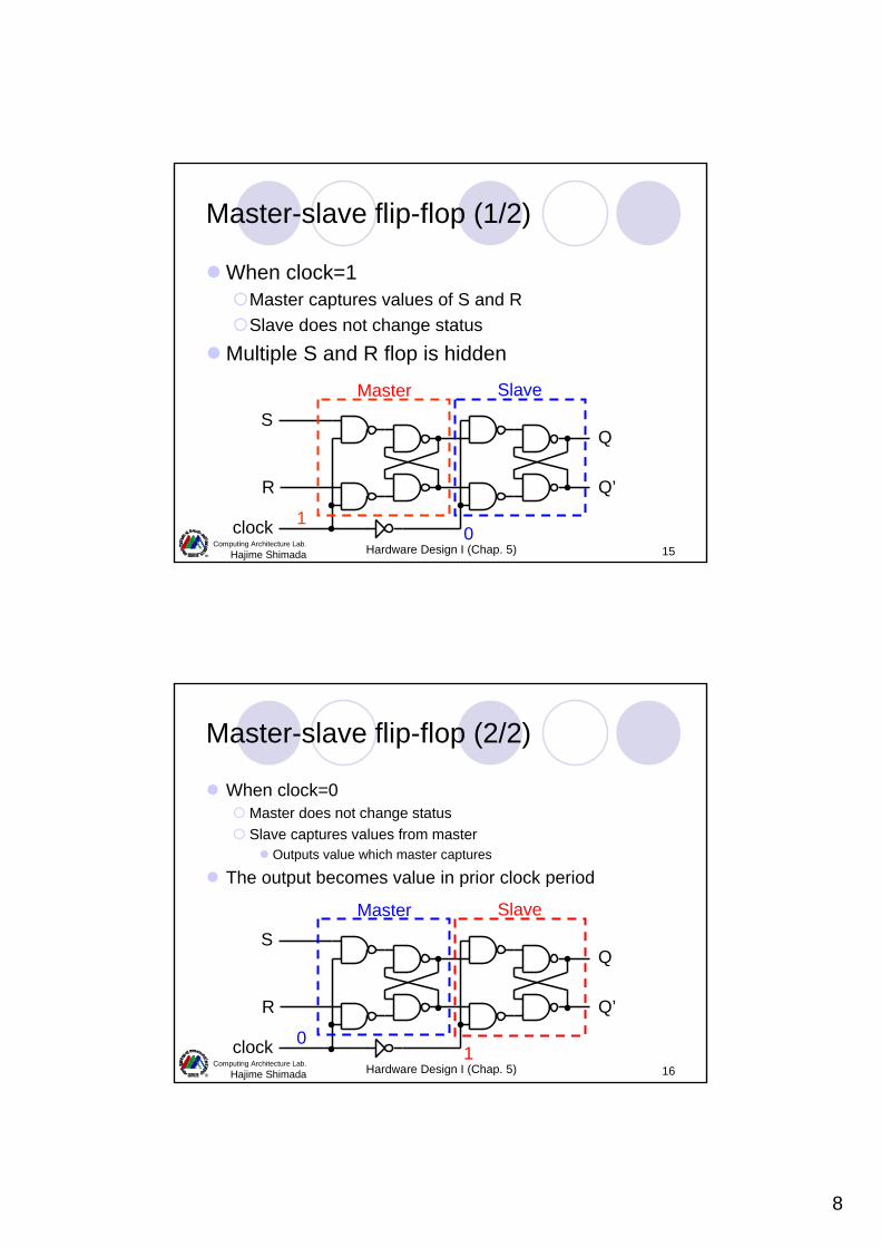
Master-slave flip-flop (1/2)
When clock=1Master captures values of S and RSlave does not change status
Multiple S and R flop is hidden
S
clock
Q
Q’R
Master Slave
01
Hardware Design I (Chap. 5) 16Computing Architecture Lab.
Hajime Shimada
Master-slave flip-flop (2/2)
When clock=0Master does not change statusSlave captures values from master
Outputs value which master captures
The output becomes value in prior clock period
S
clock
Q
Q’R
Master Slave
10
9
Hardware Design I (Chap. 5) 17Computing Architecture Lab.
Hajime Shimada
The relations of flip-flops
SR flip-flop: set/reset procedure is complicated
Clocked SR flip-flop: clock timing is severe
Master-slave SR flip-flop: dual-rail logic is redundant
Master-slave D flip-flop: delay in flip-flop is largeA part of this organization becomes D latch
Edge trigger D flip-flop
Add clock which indicate timing of value set
Accept slow clock
Simplify input to single “D”
Reduce delayNote that the latter organization
requires much more gates
Hardware Design I (Chap. 5) 18Computing Architecture Lab.
Hajime Shimada
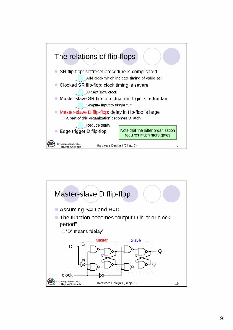
Master-slave D flip-flop
Assuming S=D and R=D’The function becomes “output D in prior clock period”
“D” means “delay”
D
clock
Q
Q’
S
R
Master Slave
10
Hardware Design I (Chap. 5) 19Computing Architecture Lab.
Hajime Shimada
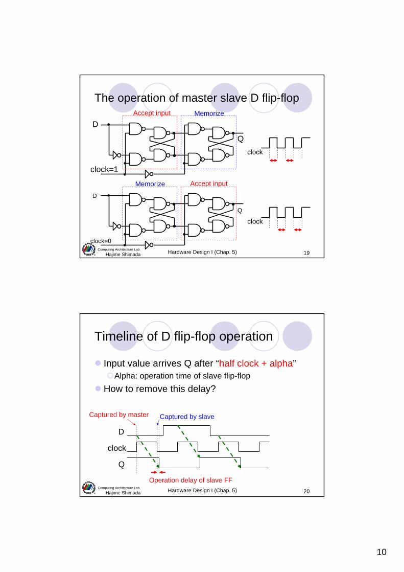
The operation of master slave D flip-flop
D
clock=0
Q
D
clock=1
Q
Accept input Memorize
clock
Accept inputMemorize
clock
Hardware Design I (Chap. 5) 20Computing Architecture Lab.
Hajime Shimada
Captured by slave
Timeline of D flip-flop operation
Input value arrives Q after “half clock + alpha”Alpha: operation time of slave flip-flop
How to remove this delay?
clock
D
Q
Captured by master
Operation delay of slave FF
11
Hardware Design I (Chap. 5) 21Computing Architecture Lab.
Hajime Shimada
The relations of flip-flops
SR flip-flop: set/reset procedure is complicated
Clocked SR flip-flop: clock timing is severe
Master-slave SR flip-flop: dual-rail logic is redundant
Master-slave D flip-flop: delay in flip-flop is largeA part of this organization becomes D latch
Edge trigger D flip-flop
Add clock which indicate timing of value set
Accept slow clock
Simplify input to single “D”
Reduce delayNote that the latter organization
requires much more gates
Hardware Design I (Chap. 5) 22Computing Architecture Lab.
Hajime Shimada
Edge trigger D flip-flop
A flip-flop which operates with edge of clockIt can output value after a moment of clock edge
A moment: state transition time of logic gatesUtilize (S,R)=(0,0) to (S,R)=(1,0) or (S,R)=(0,1) action in it
Q
clock
D
clock
Operate with this timing
12
Hardware Design I (Chap. 5) 23Computing Architecture Lab.
Hajime Shimada
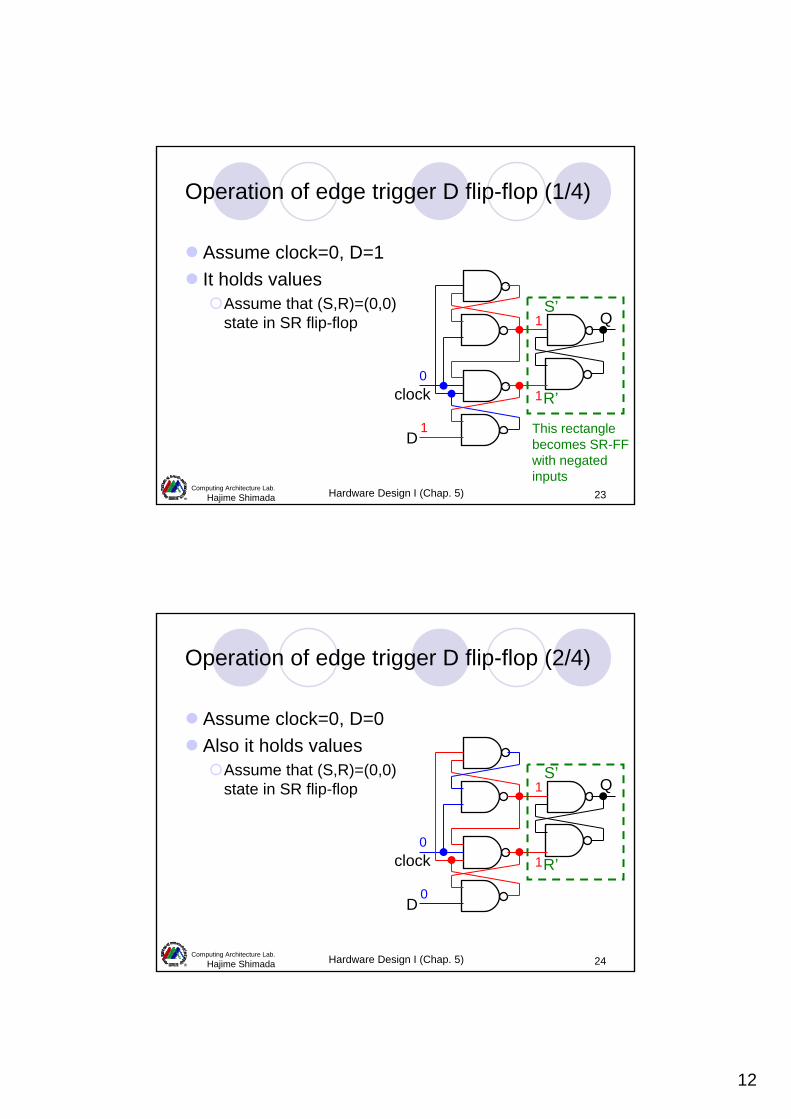
Operation of edge trigger D flip-flop (1/4)
Assume clock=0, D=1It holds values
Assume that (S,R)=(0,0) state in SR flip-flop Q
clock
D1
0
1
1
This rectanglebecomes SR-FFwith negatedinputs
S’
R’
Hardware Design I (Chap. 5) 24Computing Architecture Lab.
Hajime Shimada
Operation of edge trigger D flip-flop (2/4)
Assume clock=0, D=0Also it holds values
Assume that (S,R)=(0,0) state in SR flip-flop Q
clock
D0
0
1
1
S’
R’

13
Hardware Design I (Chap. 5) 25Computing Architecture Lab.
Hajime Shimada
Q1
1->0
Operation of edge trigger D flip-flop (3/4)
Assume clock=0->1 under D=1Q becomes 1
Assume that (S,R)=(1,0) state in SR flip-flop
clock
D1
0->11
S’
R’
Hardware Design I (Chap. 5) 26Computing Architecture Lab.
Hajime Shimada
R’1->0
Q
0->1
Operation of edge trigger D flip-flop (4/4)
Assume clock=0->1 under D=0Q becomes 0
Assume that (S,R)=(0,1) state in SR flip-flop
clock
D0
1S’
0
14
Hardware Design I (Chap. 5) 27Computing Architecture Lab.
Hajime Shimada
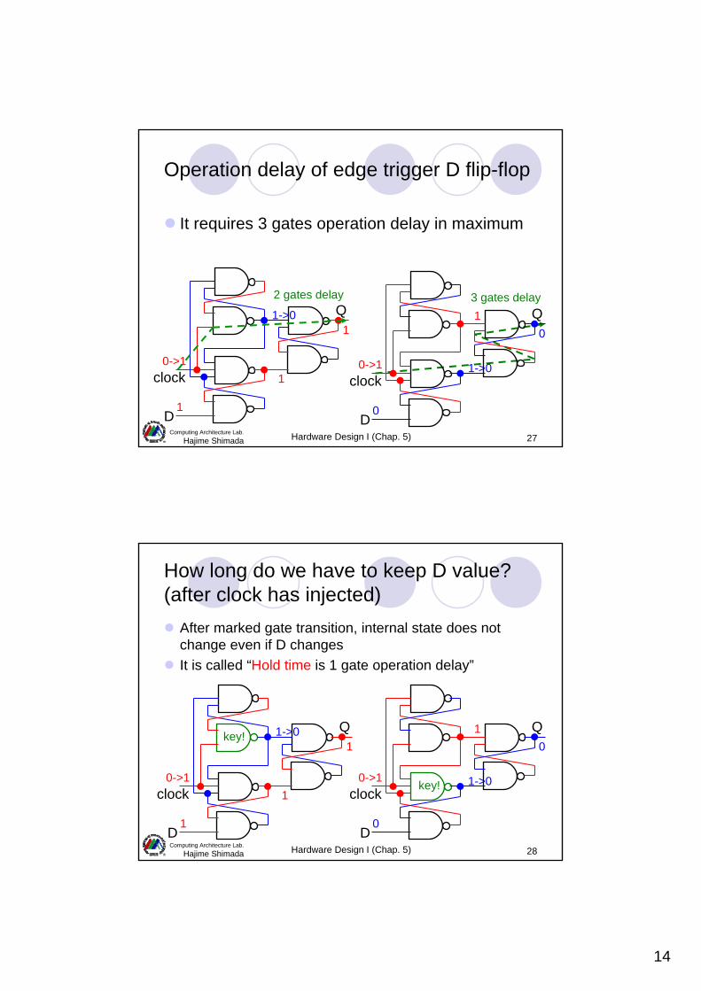
Operation delay of edge trigger D flip-flop
It requires 3 gates operation delay in maximum
Q1
1->0
clock
D1
0->11
1->0
Q
0->1clock
D0
10
3 gates delay2 gates delay
Hardware Design I (Chap. 5) 28Computing Architecture Lab.
Hajime Shimada
How long do we have to keep D value? (after clock has injected)
After marked gate transition, internal state does not change even if D changesIt is called “Hold time is 1 gate operation delay”
Q1
1->0
clock
D1
0->11
1->0
Q
0->1clock
D0
10
key!
key!

15
Hardware Design I (Chap. 5) 29Computing Architecture Lab.
Hajime Shimada
How long do we have to keep D value? (before clock has injected)
When we translate D value, it requires 2 gate delay to become ready to accept clock pulse statusIt is called “Setup time is 2 gate operation delay”
Q
clock
D1->0
0
1
1
Q
clock
D0->1
0
1
1
1->0
0->1
0->1
1->0
Hardware Design I (Chap. 5) 30Computing Architecture Lab.
Hajime Shimada
Setup time and hold time
Setup timeThe restriction before clock pulseNever change D in this term
Hold timeThe restriction after clock pulseNever change D in this term
Hold time
clock
D
Setup time Hold timeviolation
Setup timeviolation
16
Hardware Design I (Chap. 5) 31Computing Architecture Lab.
Hajime Shimada
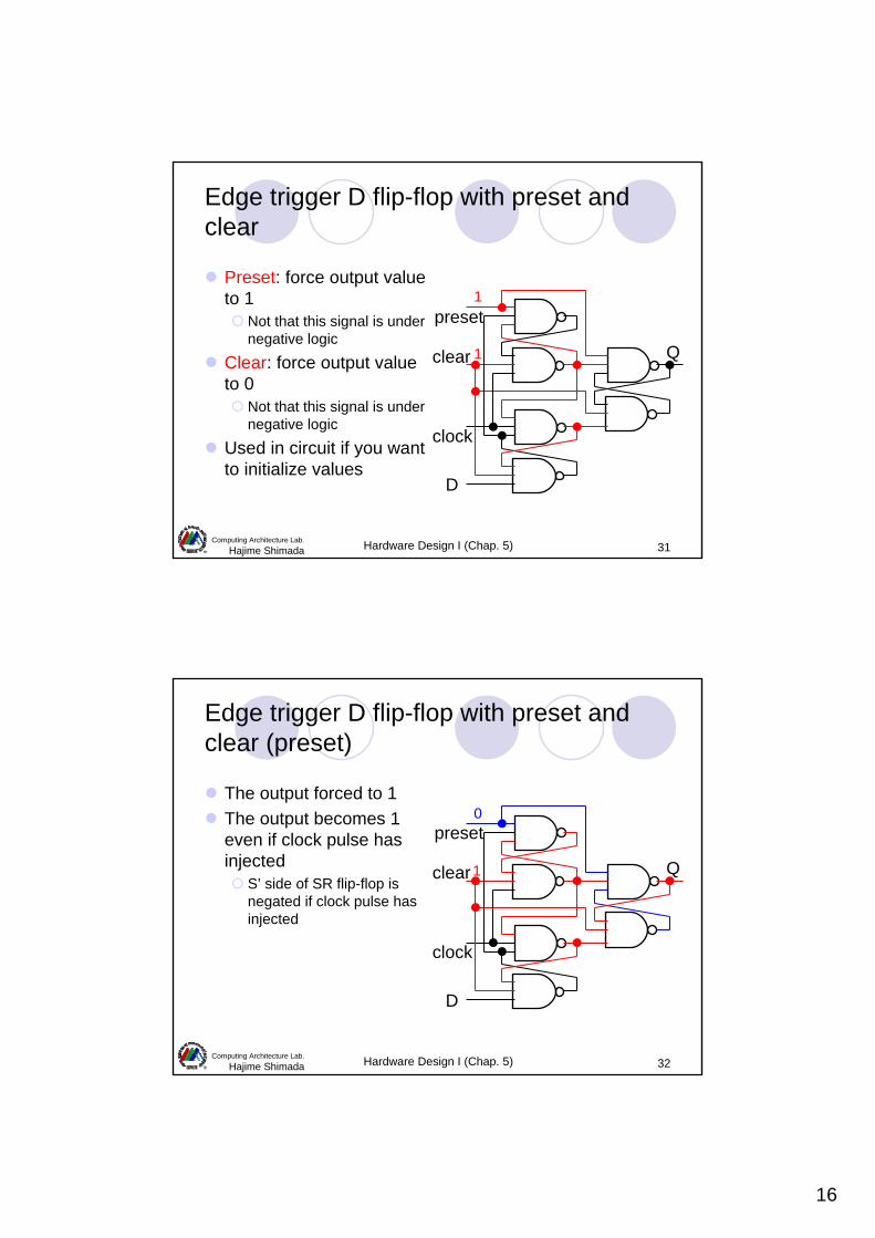
Edge trigger D flip-flop with preset and clear
Preset: force output value to 1
Not that this signal is under negative logic
Clear: force output value to 0
Not that this signal is under negative logic
Used in circuit if you want to initialize values
Qclear
clock
preset
D
1
1
Hardware Design I (Chap. 5) 32Computing Architecture Lab.
Hajime Shimada
Q
Edge trigger D flip-flop with preset and clear (preset)
The output forced to 1The output becomes 1 even if clock pulse has injected
S’ side of SR flip-flop is negated if clock pulse has injected
clear
clock
preset
D
1
0

17
Hardware Design I (Chap. 5) 33Computing Architecture Lab.
Hajime Shimada
clear0 Q
Edge trigger D flip-flop with preset and clear (clear)
The output forced to 0The output becomes 0 even if clock pulse has injected
R’ side of SR flip-flop is negated if clock pulse has injected
clock
preset
D
1
Hardware Design I (Chap. 5) 34Computing Architecture Lab.
Hajime Shimada
D latch
A part of D flip-flopThorough signal when clock=1Hold value when clock=0In some case, we utilize it in hardware design
D
clock
Q clock D Q1 0 01 1 10 * Q(previous)
18
Hardware Design I (Chap. 5) 35Computing Architecture Lab.
Hajime Shimada
Latch and flip-flop assumption in usual hardware design
In usual hardware design, we assume following function for latch and flip-flopLatch
It put through signal if clock signal is enabledIt holds last status if clock signal is not enabled
Flip-flopIt updates its status by edge of clock pulse
Hardware Design I (Chap. 5) 36Computing Architecture Lab.
Hajime Shimada
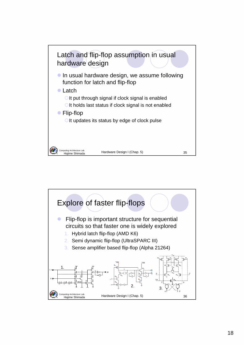
Explore of faster flip-flops
Flip-flop is important structure for sequential circuits so that faster one is widely explored1. Hybrid latch flip-flop (AMD K6)2. Semi dynamic flip-flop (UltraSPARC III)3. Sense amplifier based flip-flop (Alpha 21264)
1.
2. 3.
19
Hardware Design I (Chap. 5) 37Computing Architecture Lab.
Hajime Shimada
Outline
Flip-flops and latches (for temporal value)SR flip-flop and its variationsD flip-flop and its variationsD latch
Random Access Memory (RAM) and related structure (for storage)
Basic organization of RAMStatic RAM (SRAM)The other RAMsContent Addressable Memory (CAM)
Hardware Design I (Chap. 5) 38Computing Architecture Lab.
Hajime Shimada
What’s required for storage memory?
Data densityIf we achieve high data density, we can treat large data sizeOr we can reduce hardware cost in same data size
Data accessibilityWe can stuff data to small area if we ignore accessibility, but it is not accepted
e.g. tape device has banished because of bad accessibility
Usually, we utilize following two types organizationRandom access memory (RAM) typeContent addressable memory (CAM) type
20
Hardware Design I (Chap. 5) 39Computing Architecture Lab.
Hajime Shimada
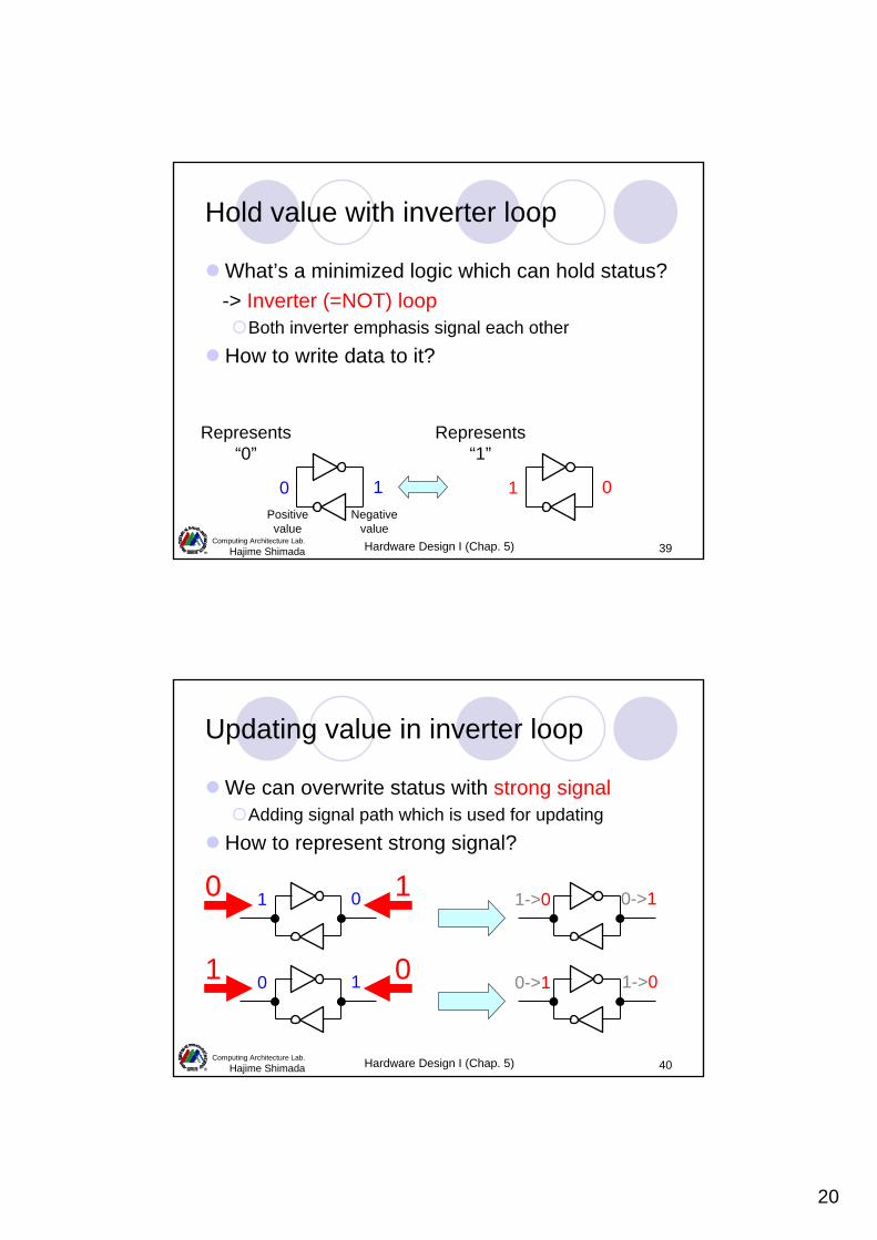
Hold value with inverter loop
What’s a minimized logic which can hold status?-> Inverter (=NOT) loop
Both inverter emphasis signal each otherHow to write data to it?
0 1 1 0
Represents“0”
Represents“1”
Positivevalue
Negativevalue
Hardware Design I (Chap. 5) 40Computing Architecture Lab.
Hajime Shimada
Updating value in inverter loop
We can overwrite status with strong signalAdding signal path which is used for updating
How to represent strong signal?
0 11 0 0->1 1->0
1 00 1 1->0 0->1

21
Hardware Design I (Chap. 5) 41Computing Architecture Lab.
Hajime Shimada
Updating value from electrical viewpoint
Prepare powerful current source to outside If precharge current is larger than discharge current of the inverter, the node becomes 1If discharge current is larger than precharge current of the inverter, the node becomes 0
0->1 1->0
0
0
1
1
Discharge
Pre-charge
1 0
1
1
0
0
Discharge
Precharge
Dis-charge
Precharge
Hardware Design I (Chap. 5) 42Computing Architecture Lab.
Hajime Shimada
Access gate (1/2)
How to control read/write operation into inverter loop?-> Utilize nMOS FET called access gate
If 0 is applied to access gate, the value does not intrudeIf 1 is applied to access gate, the value intrudes
Access gate
0 11 0
0->1 1->0
0 0
1 1
1 0
Shut out Shut out

22
Hardware Design I (Chap. 5) 43Computing Architecture Lab.
Hajime Shimada
Access gate (2/2)
Also access gate is used for reading internal value
If 0 is applied to access gate, the output becomes ZIf 1 is applied to access gate, the output becomes a value of inverter loop
0 1Z Z
0 1
0 0
1 1
0 1
Shut out Shut out
c.f. transmission gate-> Chap. 4
Hardware Design I (Chap. 5) 44Computing Architecture Lab.
Hajime Shimada
Number of transistor
The number of transistor becomes 6 in prior organization
2 x INV(2 transistors) and 2 x access gatesMuch less than flip-flops and latches
Master-slave D-FF: 36 transistors8 x NAND2(4 transistors) and 2 x INV
Edge trigger D-FF: 24 transistors6 x NAND2
D latch: 17 transistors4 x NAND2 and 1 x INV
23
Hardware Design I (Chap. 5) 45Computing Architecture Lab.
Hajime Shimada
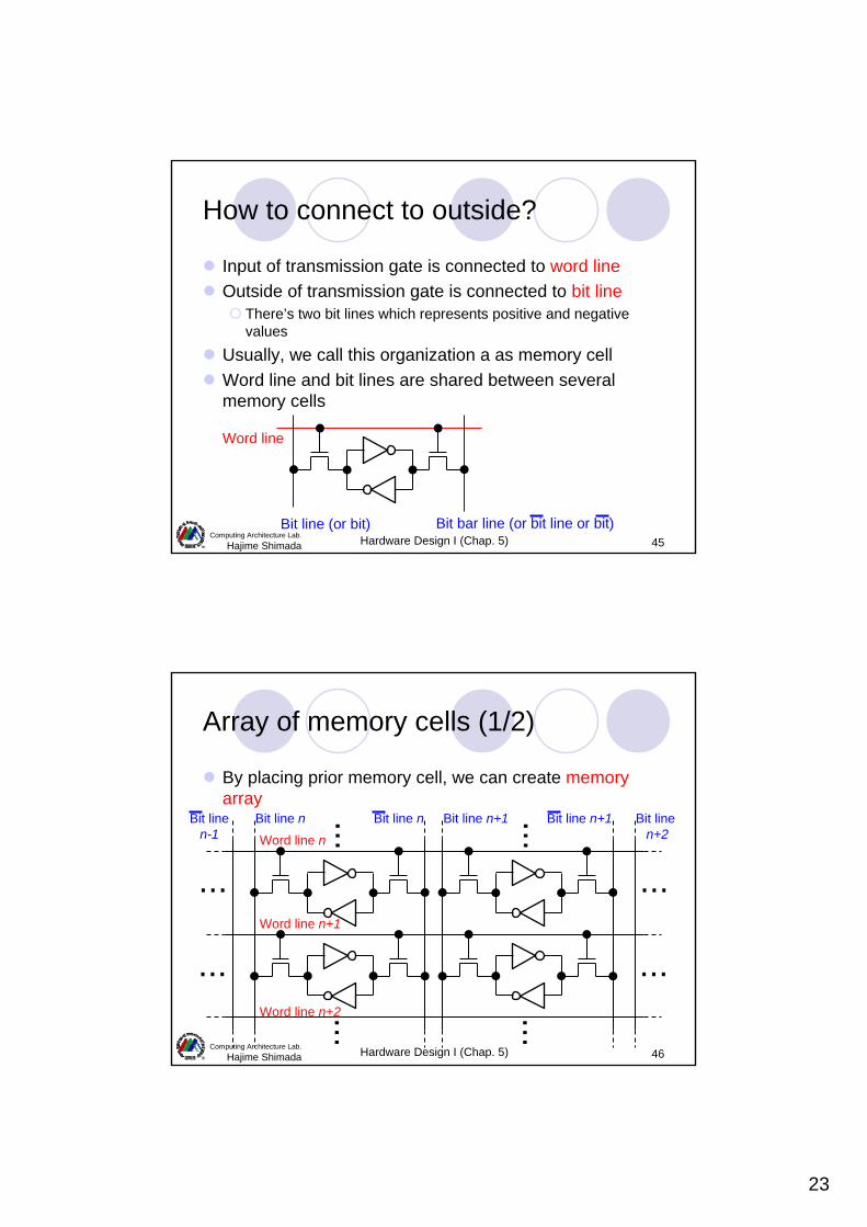
How to connect to outside?
Input of transmission gate is connected to word lineOutside of transmission gate is connected to bit line
There’s two bit lines which represents positive and negative values
Usually, we call this organization a as memory cellWord line and bit lines are shared between several memory cells
Bit line (or bit) Bit bar line (or bit line or bit)
Word line
Hardware Design I (Chap. 5) 46Computing Architecture Lab.
Hajime Shimada
Array of memory cells (1/2)
By placing prior memory cell, we can create memory array ... ...
... ...
...
...
...
...
Word line n
Word line n+1
Word line n+2
Bit line n Bit line n Bit line n+1 Bit line n+1 Bit linen+2
Bit linen-1
24
Hardware Design I (Chap. 5) 47Computing Architecture Lab.
Hajime Shimada
Array of memory cells (2/2)
e.g. A memory array which has n-bit length for vertical and m-bit length for horizontal
1-bitcell
1-bitcell
1-bitcell
1-bitcell
Bit line 0 Bit line 1Bit line
m-2Bit line
m-1
1-bitcell
1-bitcell
1-bitcell
1-bitcell
1-bitcell
1-bitcell
1-bitcell
1-bitcell
1-bitcell
1-bitcell
1-bitcell
1-bitcell
Word line 0
Word line 1
Word line n-2
Word line n-1
...
...
...
...
...... ... ...
Memoryarray
Hardware Design I (Chap. 5) 48Computing Architecture Lab.
Hajime Shimada
......
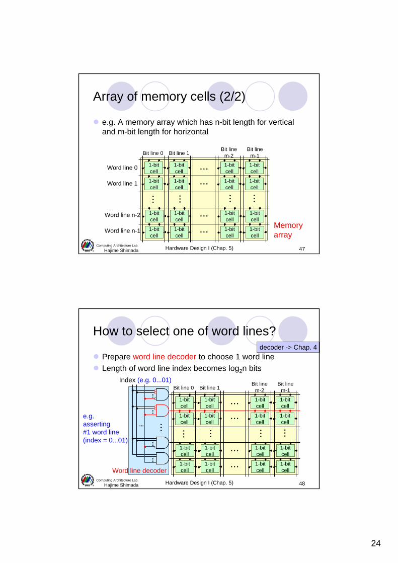
How to select one of word lines?
Prepare word line decoder to choose 1 word lineLength of word line index becomes log2n bits
1-bitcell
1-bitcell
1-bitcell
1-bitcell
Bit line 0 Bit line 1Bit line
m-2Bit line
m-1
1-bitcell
1-bitcell
1-bitcell
1-bitcell
1-bitcell
1-bitcell
1-bitcell
1-bitcell
1-bitcell
1-bitcell
1-bitcell
1-bitcell
...
...
...
...
...
... ... ...
......
......
Index (e.g. 0...01)
e.g.asserting#1 word line(index = 0...01)
Word line decoder
decoder -> Chap. 4
25
Hardware Design I (Chap. 5) 49Computing Architecture Lab.
Hajime Shimada
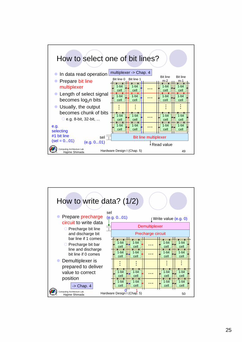
How to select one of bit lines?
In data read operationPrepare bit line multiplexerLength of select signal becomes log2n bitsUsually, the output becomes chunk of bits
e.g. 8-bit, 32-bit, ...
1-bitcell
1-bitcell
1-bitcell
1-bitcell
Bit line 0 Bit line 1Bit line
m-2Bit line
m-1
1-bitcell
1-bitcell
1-bitcell
1-bitcell
1-bitcell
1-bitcell
1-bitcell
1-bitcell
1-bitcell
1-bitcell
1-bitcell
1-bitcell
...
...
.........
... ... ...
Bit line multiplexer
e.g.selecting#1 bit line(sel = 0...01)
...sel(e.g. 0...01) Read value
multiplexer -> Chap. 4
Hardware Design I (Chap. 5) 50Computing Architecture Lab.
Hajime Shimada
How to write data? (1/2)
Prepare precharge circuit to write data
Precharge bit line and discharge bit bar line if 1 comesPrecharge bit bar line and discharge bit line if 0 comes
Demultiplexer is prepared to deliver value to correct position
1-bitcell
1-bitcell
1-bitcell
1-bitcell
1-bitcell
1-bitcell
1-bitcell
1-bitcell
1-bitcell
1-bitcell
1-bitcell
1-bitcell
1-bitcell
1-bitcell
1-bitcell
1-bitcell
...
...
...
...
...
... ... ...
Precharge circuit
Demultiplexer
Write value (e.g. 0)
10
...
sel(e.g. 0...01)
-> Chap. 4
26
Hardware Design I (Chap. 5) 51Computing Architecture Lab.
Hajime Shimada
How to write data? (2/2)
After asserting word line, the value is written into 1-bit cell
Capacitance of bit lines are enough big to overwrite value 1-bit
cell1-bitcell
1-bitcell
1-bitcell
1-bitcell
1-bitcell
1-bitcell
1-bitcell
1-bitcell
1-bitcell
1-bitcell
1-bitcell
1-bitcell
1-bitcell
1-bitcell
1-bitcell
...
......
...
...
... ... ...
Precharge circuit
Demultiplexer
Write value (e.g. 0)
10
ChargeDischarge
Hardware Design I (Chap. 5) 52Computing Architecture Lab.
Hajime Shimada
How to read value? (strictly)
Strictly speaking, read value operation is done by following operation
1. Precharge both bit lines
2. Assert word line3. The line connected
to “0” side is discharged
Why?: discharge ability is larger than precharge ability
1-bitcell
1-bitcell
1-bitcell
1-bitcell
1-bitcell
1-bitcell
1-bitcell
1-bitcell
1-bitcell
1-bitcell
1-bitcell
1-bitcell
1-bitcell
1-bitcell
1-bitcell
1-bitcell
...
...
...
...
...
... ... ...
Precharge circuit
1->0
Discharge
1
1. Precharge both bit lines2. Assert word line
-> Chap. 1

27
Hardware Design I (Chap. 5) 53Computing Architecture Lab.
Hajime Shimada
Sense amplifier (1/2)
Even if we use discharge, it requires long time to discharge bit line
Capacitance of bit line is too large for FET in 1-bit cellTo increase data density, we don’t want to increase size of FET in 1-bit cell
->Prepare sense amplifier to accelerate output
t
VBit line Bit line
Threshold voltage
Assert word lineOutput becomes 0 in bit line
Hardware Design I (Chap. 5) 54Computing Architecture Lab.
Hajime Shimada
Sense amplifier (current mirror type)A circuit which can amplifier differential of signalsCurrent flows from Vdd to Gnd in initial
Output becomes intermediate voltageOutput becomes 1 if bit begins to fallOutput falls to 0 if bit begins to fallEmphasis output signal by NOT gate
If bit lines gives some differential,output begins to fall down
Sense amplifier (2/2)
t
V
Output
Bit lineThreshold voltage
Assert word line
Current mirror typesense amplifier
Startevaluation
Bit Bit
Bit line
Output
28
Hardware Design I (Chap. 5) 55Computing Architecture Lab.
Hajime Shimada
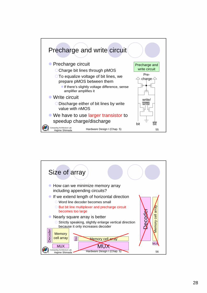
Precharge and write circuit
Precharge circuitCharge bit lines through pMOSTo equalize voltage of bit lines, we prepare pMOS between them
If there’s slightly voltage difference, sense amplifier amplifies it
Write circuitDischarge either of bit lines by write value with nMOS
We have to use larger transistor to speedup charge/discharge bit bit
Pre-charge
write/write
Precharge andwrite circuit
Hardware Design I (Chap. 5) 56Computing Architecture Lab.
Hajime Shimada
Size of array
How can we minimize memory array including appending circuits?If we extend length of horizontal direction
Word line decoder becomes smallBut bit line multiplexer and precharge circuit becomes too large
Nearly square array is betterStrictly speaking, slightly enlarge vertical direction because it only increases decoder
Dec
oder
Memory cell array
MUX
Dec
MUX
Dec
oder
MUX
Memorycell array
Mem
ory
cell
arra
y

29
Hardware Design I (Chap. 5) 57Computing Architecture Lab.
Hajime Shimada
Multiple array organization
Even if we utilize nearly square array, decoder and MUX becomes too largeIn such case, we can reduce by dividing large array to multiple sub arrays
Memorycell array
Dec
oder
MUX
Memorycell array
Dec
oder
MUX
Memorycell array
Dec
oder
MUX
Memorycell array
Dec
oder
MUX
Memorycell array
Address
Data Pre-decoderand post-MUX
Dec
oder
MUX
Hardware Design I (Chap. 5) 58Computing Architecture Lab.
Hajime Shimada
Double end and single end bit lines
Prior organization is called double endThere’s single end organization
There’s only one bit lineIt can save area But operation speed becomes slower
Sense amplifier compares voltage between bit line and Vdd
Bit line
Word line
Bit line
Word line
Single end organization
Double end organization
Bit line

30
Hardware Design I (Chap. 5) 59Computing Architecture Lab.
Hajime Shimada
Multi port memory cell (1/2)
How can I treat multiple read/write request?-> Utilize multi port memory cell
1-bitcell
1-bitcell
1-bitcell
1-bitcell
Bit line 0 Bit line 1Bit line
m-2Bit line
m-1
1-bitcell
1-bitcell
1-bitcell
1-bitcell
1-bitcell
1-bitcell
1-bitcell
1-bitcell
1-bitcell
1-bitcell
1-bitcell
1-bitcell
Word line 0
Word line 1
Word line n-2
Word line n-1
...
...
...
...
...... ... ...
Read Read
Hardware Design I (Chap. 5) 60Computing Architecture Lab.
Hajime Shimada
Multi port memory cell (2/2)
Prepare multiple word and bit linese.g. 2-port memory cellWe can send read/write request either of them
We have to prepare multiple decoder, MUX, and precharge circuits
Bit line(port 0)
Bit line(port 0)
Word line(port 0)
Word line(port 1)
Bit line(port 1)
Bit line(port 1)

31
Hardware Design I (Chap. 5) 61Computing Architecture Lab.
Hajime Shimada
Multi-bank organization (1/2)
An another method to treat multiple read/write request
Allocate data to different bank
Usually, consecutive data in memory address are allocated to different bank
Allow multiple read/write if data exist in different bank
Also used for increase memory band width
Increase read/write request per unit time
Also called “interleaving”D
ecod
er
MUX
Memorycell array
Dec
oder
MUX
Memorycell array
Dec
oder
MUX
Memorycell array
Dec
oder
MUX
Memorycell array
Address(x4 in max.)
Data (x4 in max.)
Bank 0 Bank 1
Bank 2 Bank 3
Addr. 1Data 1
Addr. 2
Data 2
e.g. treating 2 read/write req.
Hardware Design I (Chap. 5) 62Computing Architecture Lab.
Hajime Shimada
Multi bank organization (2/2)
If read/write requests are concentrated to one bank, we can only allow one of them
Called “conflict”Pre-decoder treat arbitration of themAlso, hardware which send read/write request must consider data delay caused by conflict
Dec
oder
MUX
Memorycell array
Dec
oder
MUX
Memorycell array
Dec
oder
MUX
Memorycell array
Dec
oder
MUX
Memorycell array
Address(x4 in max.)Data (x4 in max)
Bank 0 Bank 1
Bank 2 Bank 3
Addr. 1Addr. 2
Conflict!
32
Hardware Design I (Chap. 5) 63Computing Architecture Lab.
Hajime Shimada
Several RAMs
The prior organization is called SRAM (Static Random Access Memory)There’s several type of RAMs
Dynamic RAM (DRAM)Flash memoryOther advanced RAMs
Hardware Design I (Chap. 5) 64Computing Architecture Lab.
Hajime Shimada
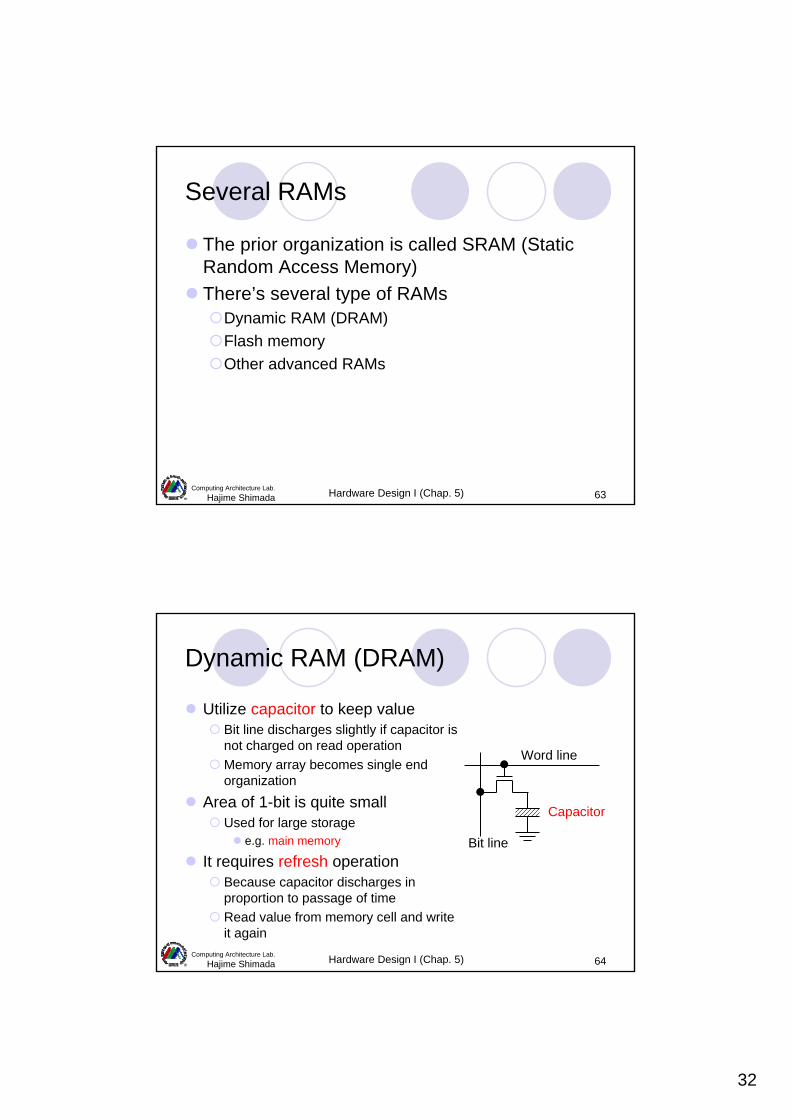
Dynamic RAM (DRAM)
Utilize capacitor to keep valueBit line discharges slightly if capacitor is not charged on read operation Memory array becomes single end organization
Area of 1-bit is quite smallUsed for large storage
e.g. main memory
It requires refresh operationBecause capacitor discharges in proportion to passage of timeRead value from memory cell and write it again
Bit line
Word line
Capacitor
33
Hardware Design I (Chap. 5) 65Computing Architecture Lab.
Hajime Shimada
Quiz
How many bits can latest DRAM hold?1. 4G bits2. 8G bits3. 16G bits4. 32G bits
Hardware Design I (Chap. 5) 66Computing Architecture Lab.
Hajime Shimada
Answer
1. “4G bits”Comparatively low capacity than following flash memory
34
Hardware Design I (Chap. 5) 67Computing Architecture Lab.
Hajime Shimada
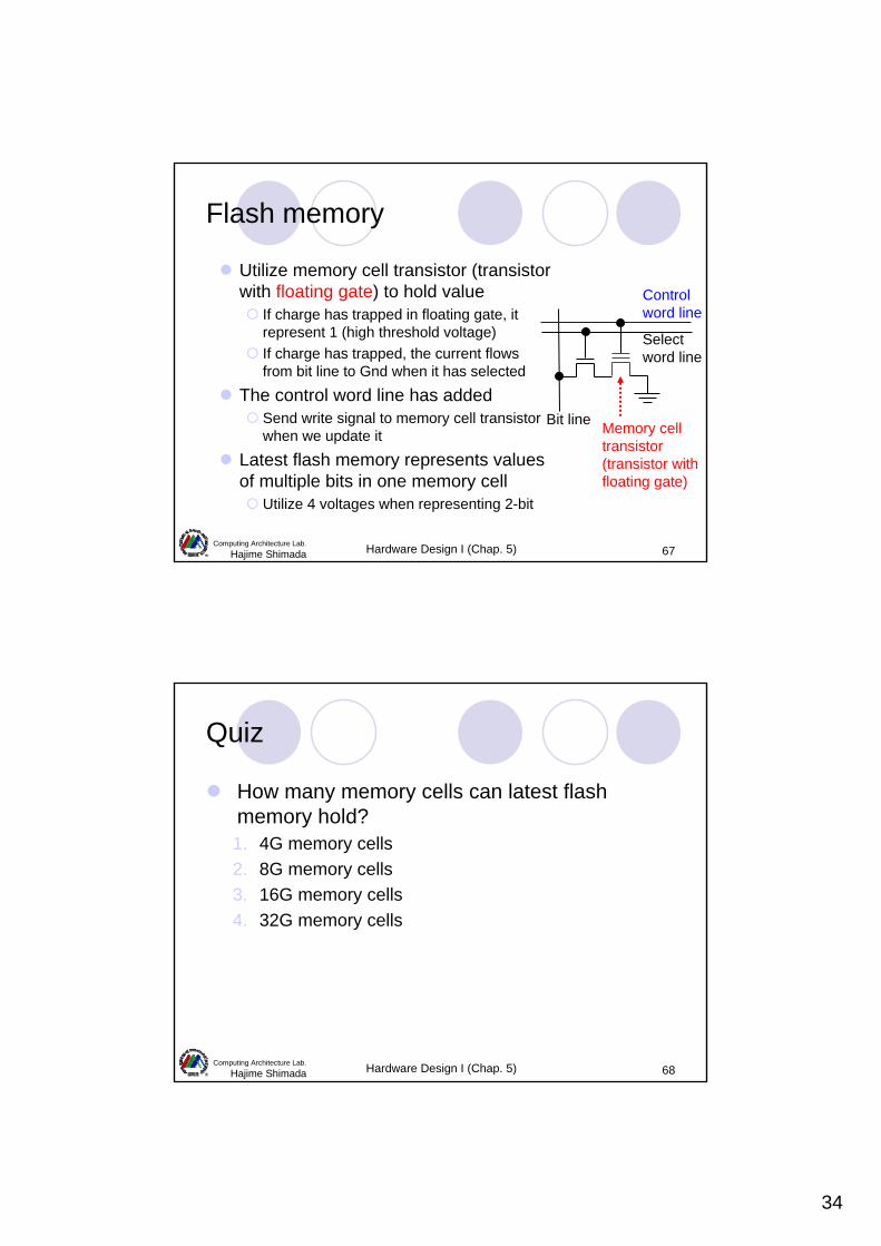
Flash memory
Utilize memory cell transistor (transistor with floating gate) to hold value
If charge has trapped in floating gate, it represent 1 (high threshold voltage)If charge has trapped, the current flows from bit line to Gnd when it has selected
The control word line has addedSend write signal to memory cell transistor when we update it
Latest flash memory represents valuesof multiple bits in one memory cell
Utilize 4 voltages when representing 2-bit
Bit line
Select word line
Control word line
Memory celltransistor(transistor withfloating gate)
Hardware Design I (Chap. 5) 68Computing Architecture Lab.
Hajime Shimada
Quiz
How many memory cells can latest flash memory hold?1. 4G memory cells2. 8G memory cells3. 16G memory cells4. 32G memory cells
35
Hardware Design I (Chap. 5) 69Computing Architecture Lab.
Hajime Shimada
Answer
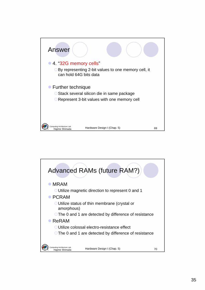
4. “32G memory cells”By representing 2-bit values to one memory cell, it can hold 64G bits data
Further techniqueStack several silicon die in same packageRepresent 3-bit values with one memory cell
Hardware Design I (Chap. 5) 70Computing Architecture Lab.
Hajime Shimada
Advanced RAMs (future RAM?)
MRAMUtilize magnetic direction to represent 0 and 1
PCRAMUtilize status of thin membrane (crystal or amorphous)The 0 and 1 are detected by difference of resistance
ReRAMUtilize colossal electro-resistance effectThe 0 and 1 are detected by difference of resistance

36
Hardware Design I (Chap. 5) 71Computing Architecture Lab.
Hajime Shimada
CAM (Content Addressable Memory)
A circuit which can compare input value and content of memory
Operate multiple comparison simultaneouslyUsage: packet matching in network router, tag matching, ...
Achieve by adding some circuits to RAM
Match lineMatch data line and its negationPull down stacks
Word line
Matchdata line
Match lineMatch
data line
Bit Bit1-bit cell of CAM
Pull down stacks
Hardware Design I (Chap. 5) 72Computing Architecture Lab.
Hajime Shimada
Match operation
Firstly we charge match line and put match data to match data lineIf it does not match, match line discharged to 0Other wise match line keeps 1e.g. Content of memory is 1 and match data is 0
-> Match line is discharged through left pull down stack
Word line
Matchdata
Match lineMatchdata
Bit Bit
1 0
1 0Discharge
37
Hardware Design I (Chap. 5) 73Computing Architecture Lab.
Hajime Shimada
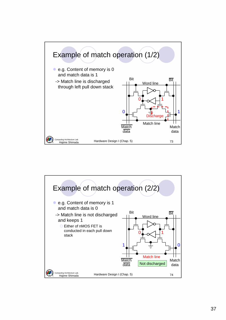
Example of match operation (1/2)
e.g. Content of memory is 0 and match data is 1
-> Match line is discharged through left pull down stack
Word line
Matchdata
Match lineMatchdata
Bit Bit
0 1
0 1Discharge
Hardware Design I (Chap. 5) 74Computing Architecture Lab.
Hajime Shimada
Example of match operation (2/2)
e.g. Content of memory is 1 and match data is 0
-> Match line is not discharged and keeps 1
Either of nMOS FET is conducted in each pull down stack
Word line
Matchdata
Match lineMatchdata
Bit Bit
0 1
1 0
Not discharged
38
Hardware Design I (Chap. 5) 75Computing Architecture Lab.
Hajime Shimada
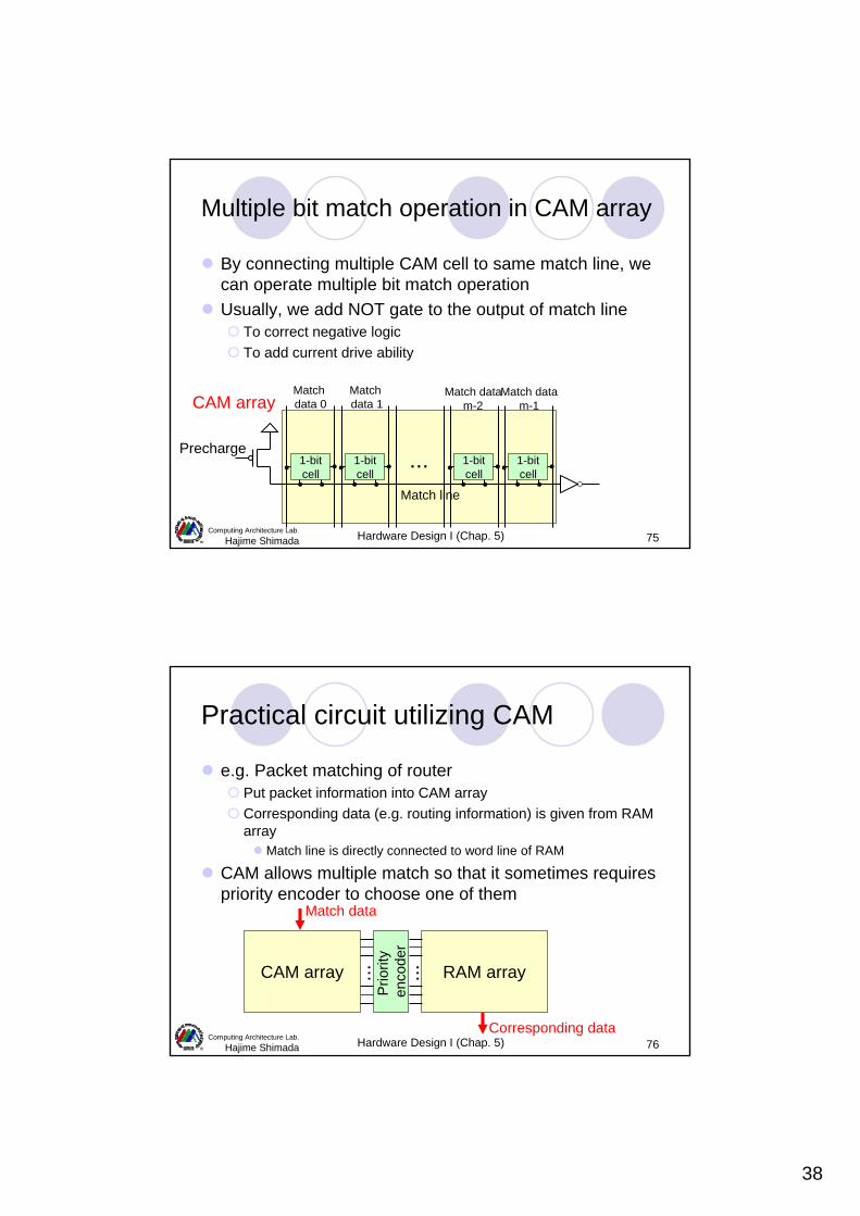
Multiple bit match operation in CAM array
By connecting multiple CAM cell to same match line, we can operate multiple bit match operationUsually, we add NOT gate to the output of match line
To correct negative logicTo add current drive ability
CAM arrayMatchdata 0
Matchdata 1
Match datam-2
Match datam-1
1-bitcell
1-bitcell
1-bitcell
1-bitcell
Match line
...Precharge
Hardware Design I (Chap. 5) 76Computing Architecture Lab.
Hajime Shimada
Practical circuit utilizing CAM
e.g. Packet matching of routerPut packet information into CAM arrayCorresponding data (e.g. routing information) is given from RAM array
Match line is directly connected to word line of RAM
CAM allows multiple match so that it sometimes requires priority encoder to choose one of them
CAM array RAM array
Prio
rity
enco
der
Match data
Corresponding data
... ...