Embed Size (px)
Citation preview
1
HEXAGONAL BORON NITRIDE VACANCIES AS ANENHANCED SINGLE PHOTON SOURCE
Guy LeckenbySupervisor: Marcus Doherty
PhB Advanced Studies Extension, Research School of Physics & EngineeringThe Australian National University, Canberra, ACT 2611, Australia
April 10, 2017
ABSTRACT
Single photon sources are highly sought after as the first building blocks in a wide variety of quantum technologies. Wepresent hexagonal boron nitride (hBN) defects as a potential single photon source for use in such applications. hBN is a promisingsingle photon source due to its 2-dimensional resilient structure, narrow zero phonon line, and ultrabright count rate of 4.2× 10⁶
counts s−1. Furthermore, we demonstrate the design of a high finesse fibre microcavity which can be coupled to hBN to enhancethe spontaneous emission rate via the Purcell effect. By analysing this coupling, we deduce that a maximum Purcell factor of14.41 is attainable at a cavity length of 0.3115 µm. Thus we conclude that cavity enhancement of single photon sources has thepotential for order of magnitude increase in count rate.
I. INTRODUCTION
Quantum technologies have gathered extensive interest overthe past few decades for the ability to revolutionise cryptogra-phy, computation speed and information transfer. However thelarge majority of these applications inherently require a stablesingle photon source (SPS) that can be triggered on demand.These purely quantum properties are difficult to access and haveonly recently even been observed with the first observations ofphoton counting statistics occurring just 40 years ago (Kimbleet. al., 1977). Today there are numerous processes availableincluding diamond vacancy centres, quantum dots, carbonnanotubes, and florescence of a wide range of other quantumsystems (Aharonovich et. al., 2011).
Single photons are used broadly in quantum applicationsbecause their quantum states are easily manipulable (e.g.polarisation), they are weakly interacting thus preservingquantum states over long distances, and are energy efficientin production (although some SPSs require significant energyinput). In particular polarisation states are easy to manipulateand are thus used widely in simple implementations of quantumtechnologies. In quantum cryptography, quantum key distribu-tion uses polarization of single photons as the transmissionmechanism for both BB84 or B92 encryption protocols andentangled state cryptography (Naik et. al., 2000). Most of thebasic implementations of qubits for quantum computing requiresingle photon sources which are manipulated by linear opticalcomponents. More advanced methods like NMR systems, iontraps, quantum dots and superconducting systems use trappedphotons rather than SPSs (Fox, 2006). SPSs can also be usedto test Bell’s inequality and investigate quantum teleportationthrough the Hong-Ou-Mandel interferometer (Fox, 2006).
An ideal single photon source emits one photon on demand.In quantum cryptography, any deviation from a single photongenerates error and potential for successful eavesdropping (Fox,2006). In quantum computing, multiple photons introduce extrastates which alters the effects of quantum gates on qubits.However there are several other metrics that constitute the
suitability of an ideal SPS. Aharonovich et. al. (2011) focuson six important factors:
1) Stable emission, that is free from blinking (varyingintensity) or bleaching (reduction of luminescence due toother reactions).
2) A narrow phonon linewidth with the majority of lumines-cence in the zero phonon line providing indistinguishablephotons
3) A short excited state lifetime (ps < τ < ns) for betterantibunching rates.
4) Fully polarised in absorption and emission channels whichis required for practical quantum cryptography.
5) Two level system with non shelving or metastable stategenerating reliable radiative emission.
6) Negligible dephasing and spectral diffusion to produceenduring identical photons.
Whilst there is no perfect SPS, there are many systems whichmake good approximations. Each has their own advantagesand disadvantages, however one system type that is attractingextensive research currently are vacancy centres because oftheir photostable emission, room temperature operation andlong coherence times (Aharonovich et. al., 2011).
II. HBN AS A SINGLE PHOTON SOURCE
This report will focus on nitrogen vacancies in hexagonalboron nitride (hBN). hBN is of particular interest as it was thefirst two-dimensional material to demonstrate room temperaturesingle photons and generates both polarised and ultra brightemission (Tran et. al., 2015). This 2 dimensionality is importantfor compact applications such a photonic circuits on singlechips. The large bandgap of hBN allows for defects withrelatively narrow zero phonon linewidths of about 10nmat room temperature (Tran et. al., 2015). Furthermore thedefects are localised for precise applications and are highlyrobust, being able to withstand aggressive annealing in bothoxidising and reducing environments (Tran et. al., 2016). This
G. Leckenby hBN as a Single Photon Source 2
(a) Room temperature luminescence spectra (b) Second-order autocorrelation data.
Figure 1: Spectroscopic data of a localised defect for mono- and multilayer hBN (Tran et. al., 2015).
sets hBN up as an important SPS for quantum information andnanophotonic applications.
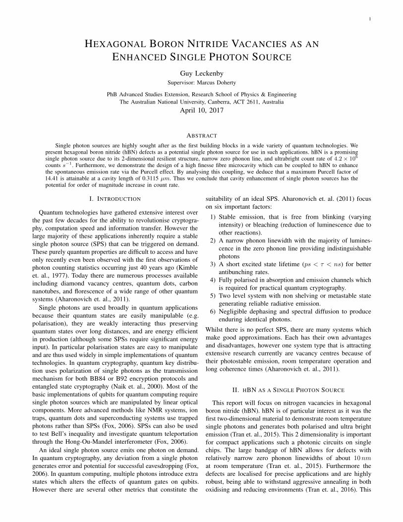
hBN has a wide bandgap of 6 eV which houses severaldefects. Tran et. al. (2015) identified three candidates for theobserved optical defects; a nitrogen vacancy (VN ), a boronvacancy (VB), or an anti-site complex where a nitrogen occupiesa boron site and the nitrogen site is left vacant (NBVN ). Bymodelling band gap transitions, Tran et. al. (2015) concludedthat the NBVN defect is the most probable candidate for theobserved optical emission and that the other vacancies willemit at non-optical wavelengths. The structure of the NBVNdefect in the 2D hBN lattice is seen in Figure 2.
Figure 2: Molecular structure of the NBVN defectwithin the hBN lattice (Tran et. al., 2015).
The observed spectrum (Tran et. al., 2015) of the NBVNdefect in hBN (hereby we shall refer to NBVN as simplythe defect) is shown in Figure 1a. In both the mono- andmultilayer cases, a bright peak is observed at ∼ 623nm. In themonolayer case, it is significantly broadened and asymmetricwhich is not ideal for SPS applications. However the dominantexcitation peak narrows significantly in the multilayer casewhere the zero phonon line (ZPL) has a FWHM of . 10nm.The multilayer defect also exhibits a phonon side band (PSB)doublet at 680nm and 693nm which yields a Debye-Waller(DW) factor of ∼ 0.82 which is among the highest for vacancycentres. Simple NV centres in diamond have DW factors of0.04 however SiV and CrV can demonstrate DW factors ashigh as 0.8 (Aharonovich et. al, 2011).
SPSs are traditionally tested using Hanbury, Brown, & Twiss(HBT) interferometry to measure the second-order autocorrela-
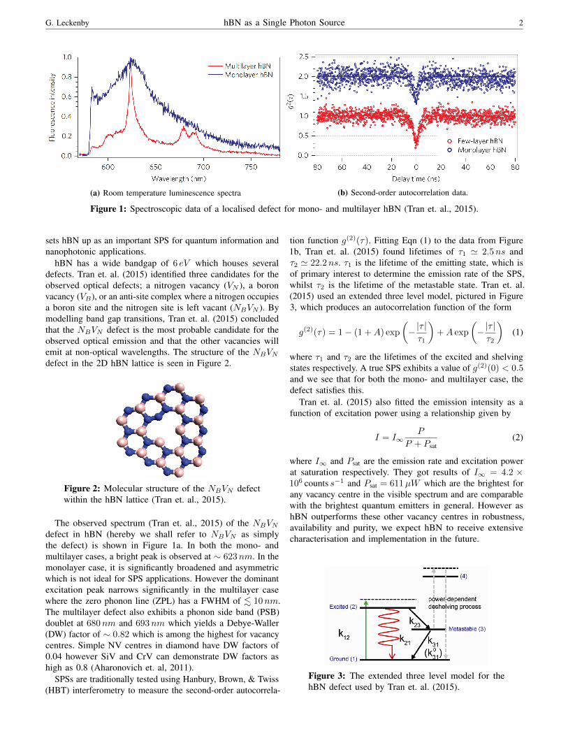
tion function g(2)(τ). Fitting Eqn (1) to the data from Figure1b, Tran et. al. (2015) found lifetimes of τ1 ' 2.5ns andτ2 ' 22.2ns. τ1 is the lifetime of the emitting state, which isof primary interest to determine the emission rate of the SPS,whilst τ2 is the lifetime of the metastable state. Tran et. al.(2015) used an extended three level model, pictured in Figure3, which produces an autocorrelation function of the form
g(2)(τ) = 1− (1 +A) exp
(−|τ |τ1
)+A exp
(−|τ |τ2
)(1)
where τ1 and τ2 are the lifetimes of the excited and shelvingstates respectively. A true SPS exhibits a value of g(2)(0) < 0.5and we see that for both the mono- and multilayer case, thedefect satisfies this.
Tran et. al. (2015) also fitted the emission intensity as afunction of excitation power using a relationship given by
I = I∞P
P + Psat(2)
where I∞ and Psat are the emission rate and excitation powerat saturation respectively. They got results of I∞ = 4.2 ×10⁶ counts s−1 and Psat = 611µW which are the brightest forany vacancy centre in the visible spectrum and are comparablewith the brightest quantum emitters in general. However ashBN outperforms these other vacancy centres in robustness,availability and purity, we expect hBN to receive extensivecharacterisation and implementation in the future.
Figure 3: The extended three level model for thehBN defect used by Tran et. al. (2015).
G. Leckenby hBN as a Single Photon Source 3
III. CAVITY ENHANCEMENT
Alongside the single photon sources themselves, microcavi-ties are attracting attention due to their ability to enhance thedesirable properties of the SPSs. In particular, the Purcell effectcan be used to enhance the spontaneous emission rate of theSPS. This reduces the relaxation time after excitation whichin turn produces a more controlled and regular emission ofphotons.
Depending on the parameters of the cavity, the cavitymodes will either be close to or far from resonance for theconsidered transition. In particular, the photon density of stateswill be higher near cavity modes and thus the probability ofspontaneous emission will be higher near cavity modes. Thisserves to either suppress or enhance the spontaneous emissionof system (Fox, 2006). This effect, known in the weak couplingregime as the Purcell effect, can be succinctly expressed inthe Purcell Factor which is a comparison of the spontaneousemission rate for the cavity with free space:
FP ≡τ freeR
τ cavR
=3Q(λ/n)3
4π2V0
∫ξ2∆ω2
cL(ω0)
4(ω0 − ωc)2 + ∆ω2c
dω0 (3)
where L(ω0) is the transition lineshape, ω0 the transitionfrequency and ωc the cavity mode frequency, Q the qualityfactor, V0 the cavity volume, λ the free-space wavelength ofthe transition, n the refractive index of the cavity, and ξ is theis the normalised dipole orientation factor. Values of FP > 1imply enhanced spontaneous emission whilst FP < 1 impliessuppressed emission.
IV. FIBRE MICROCAVITIES
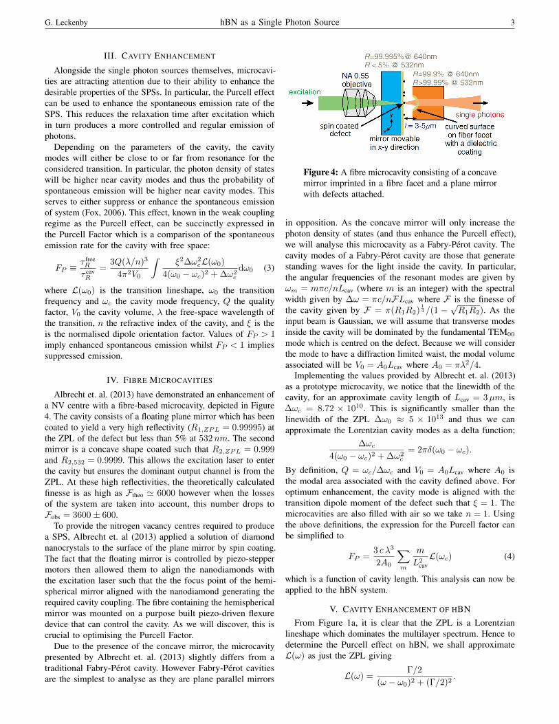
Albrecht et. al. (2013) have demonstrated an enhancement ofa NV centre with a fibre-based microcavity, depicted in Figure4. The cavity consists of a floating plane mirror which has beencoated to yield a very high reflectivity (R1,ZPL = 0.99995) atthe ZPL of the defect but less than 5% at 532nm. The secondmirror is a concave shape coated such that R2,ZPL = 0.999and R2,532 = 0.9999. This allows the excitation laser to enterthe cavity but ensures the dominant output channel is from theZPL. At these high reflectivities, the theoretically calculatedfinesse is as high as Ftheo ' 6000 however when the lossesof the system are taken into account, this number drops toFobs = 3600± 600.
To provide the nitrogen vacancy centres required to producea SPS, Albrecht et. al (2013) applied a solution of diamondnanocrystals to the surface of the plane mirror by spin coating.The fact that the floating mirror is controlled by piezo-steppermotors then allowed them to align the nanodiamonds withthe excitation laser such that the the focus point of the hemi-spherical mirror aligned with the nanodiamond generating therequired cavity coupling. The fibre containing the hemisphericalmirror was mounted on a purpose built piezo-driven flexuredevice that can control the cavity. As we will discover, this iscrucial to optimising the Purcell Factor.
Due to the presence of the concave mirror, the microcavitypresented by Albrecht et. al. (2013) slightly differs from atraditional Fabry-Perot cavity. However Fabry-Perot cavitiesare the simplest to analyse as they are plane parallel mirrors
Figure 4: A fibre microcavity consisting of a concavemirror imprinted in a fibre facet and a plane mirrorwith defects attached.
in opposition. As the concave mirror will only increase thephoton density of states (and thus enhance the Purcell effect),we will analyse this microcavity as a Fabry-Perot cavity. Thecavity modes of a Fabry-Perot cavity are those that generatestanding waves for the light inside the cavity. In particular,the angular frequencies of the resonant modes are given byωm = mπc/nLcav (where m is an integer) with the spectralwidth given by ∆ω = πc/nFLcav where F is the finesse ofthe cavity given by F = π(R1R2)
14 /(1 −
√R1R2). As the
input beam is Gaussian, we will assume that transverse modesinside the cavity will be dominated by the fundamental TEM00
mode which is centred on the defect. Because we will considerthe mode to have a diffraction limited waist, the modal volumeassociated will be V0 = A0Lcav where A0 = πλ2/4.
Implementing the values provided by Albrecht et. al. (2013)as a prototype microcavity, we notice that the linewidth of thecavity, for an approximate cavity length of Lcav = 3µm, is∆ωc = 8.72 × 10¹⁰. This is significantly smaller than thelinewidth of the ZPL ∆ω0 ≈ 5 × 10¹³ and thus we canapproximate the Lorentzian cavity modes as a delta function;
∆ωc
4(ω0 − ωc)2 + ∆ω2c
= 2πδ(ω0 − ωc).
By definition, Q = ωc/∆ωc and V0 = A0Lcav where A0 isthe modal area associated with the cavity defined above. Foroptimum enhancement, the cavity mode is aligned with thetransition dipole moment of the defect such that ξ = 1. Themicrocavities are also filled with air so we take n = 1. Usingthe above definitions, the expression for the Purcell factor canbe simplified to
FP =3 c λ3
2A0
∑m
m
L2cavL(ωc) (4)
which is a function of cavity length. This analysis can now beapplied to the hBN system.
V. CAVITY ENHANCEMENT OF HBNFrom Figure 1a, it is clear that the ZPL is a Lorentzian
lineshape which dominates the multilayer spectrum. Hence todetermine the Purcell effect on hBN, we shall approximateL(ω) as just the ZPL giving
L(ω) =Γ/2
(ω − ω0)2 + (Γ/2)2.
G. Leckenby hBN as a Single Photon Source 4
0 1 2 3 4 5
0
5
10
15
Cavity Length (μm)
PurcellFactor
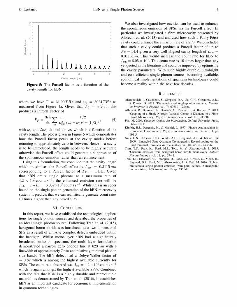
Figure 5: The Purcell factor as a function of thecavity length for hBN.
where we have Γ = 31.90THz and ω0 = 3024THz asmeasured from Figure 1a. Given that A0 = πλ2/4, thisproduces a Purcell Factor of
FP =3cλ
8π
∑m
m
L2cav
Γ/2
(ωc − ω0)2 + (Γ/2)2, (5)
with ωc and ∆ωc defined above, which is a function of thecavity length. The plot is given in Figure 5 which demonstrateshow the Purcell factor peaks at the cavity modes beforereturning to approximately zero in between. Hence if a cavityis to be introduced, the length needs to be highly accurateotherwise the Purcell effect could generate a suppression ofthe spontaneous emission rather than an enhancement.
Using this formulation, we conclude that the cavity lengthwhich maximises the Purcell effect is Lcav = 0.3115µmcorresponding to a Purcell factor of FP = 14.41. Giventhat hBN emits single photons at a maximum rate of4.2 × 106 counts s−1, the enhanced emission rate will beIenh = FP I∞ = 6.052×10⁷ counts s−1. Whilst this is an upperbound on the single photon generation of the hBN-microcavitysystem, it predicts that we can realistically generate count rates10 times higher than any naked SPS.
VI. CONCLUSION
In this report, we have established the technological applica-tions for single photon sources and described the properties ofan ideal single photon source. Following Tran et. al. (2015),hexagonal boron nitride was introduced as a two dimensionalSPS as a result of anti-site complex defects embedded withinthe bandgap. Whilst mono-layer hBN had a significantlybroadened emission spectrum, the multi-layer formulationdemonstrated a narrow zero phonon line at 623nm with alinewidth of approximately 7nm and relatively minimal phononside bands. The hBN defect had a Debye-Waller factor of∼ 0.82 which is among the highest available currently forSPSs. The count rate observed was I∞ = 4.2× 10⁶ counts s−1
which is again amongst the highest available SPSs. Combinedwith the fact that hBN is a highly durable and reproduciblematerial, as demonstrated by Tran et. al. (2016), it establisheshBN as an important candidate for economical implementationin quantum technologies.
We also investigated how cavities can be used to enhancethe spontaneous emission of SPSs via the Purcell effect. Inparticular we investigated a fibre microcavity presented byAlbrecht et. al. (2013) and analysed how such a Fabry-Perotcavity could enhance the emission rate of a SPS. We concludedthat such a cavity could produce a Purcell factor of up toFP = 14.4 given a very well aligned cavity length of Lcav =0.3115µm. This would increase the count rate for hBN toIenh = 6.05× 10⁷. This count rate is 10 times larger than anyyet quoted in the literature and could be improved by optimisingthe cavity parameters. With such highly durable, ultrabrightand cost efficient single photon sources becoming available,economical implementations of quantum technologies couldbecome a reality within the next few decades.
REFERENCES
Aharonovich, I., Castelletto, S., Simpson, D.A., Su, C-H., Greentree, A.D.,& Prawler, S. 2011. ‘Diamond-based single-photon emitters,’ Reportson Progress in Physics, vol. 74 076501 (28pp).
Albrecht, R., Bommer, A., Deutsch, C., Reichel, J., & Becher, C. 2013.‘Coupling of a Single Nitrogen-Vacancy Centre in Diamond to a Fibre-Based Microcavity,’ Physical Review Letters, vol. 110, 243602.
Fox, M. 2006. Quantum Optics: An Introduction, Oxford University Press,Oxford, NY.
Kimble, H.J., Dagenais, M., & Mandel, L. 1977. ‘Photon Antibunching inResonance Fluorescence,’ Physical Review Letters, vol. 39, no. 11, pp.691-5.
Naik, D.S., Peterson, C.G., White, A.G., Berglund, A.J., & Kwiat, P.G.2000. ‘Entangled State Quantum Cryptography: Eavesdropping on theEkert Protocol,’ Physical Review Letters, vol. 84, no. 20, 4733-6.
Tran, T.T., Bray, K., Ford, M.J., Toth, M. & Aharonovich, I. 2015.‘Quantum emission from hexagonal boron nitride monolayers,’ Nature:Nanotechnology, vol. 11, pp. 37-41.
Tran, T.T., Elbadawi, C., Totonjian, D., Lobo, C.J., Grosso, G., Moon, H.,Englund, D.R., Ford, M.J., Aharonovich, I., & Toth, M. 2016. ‘Robustmulticolour single photon emission from point defects in hexagonalboron nitride,’ ACS Nano, vol. 10, -p. 7331-8.