Embed Size (px)
Citation preview
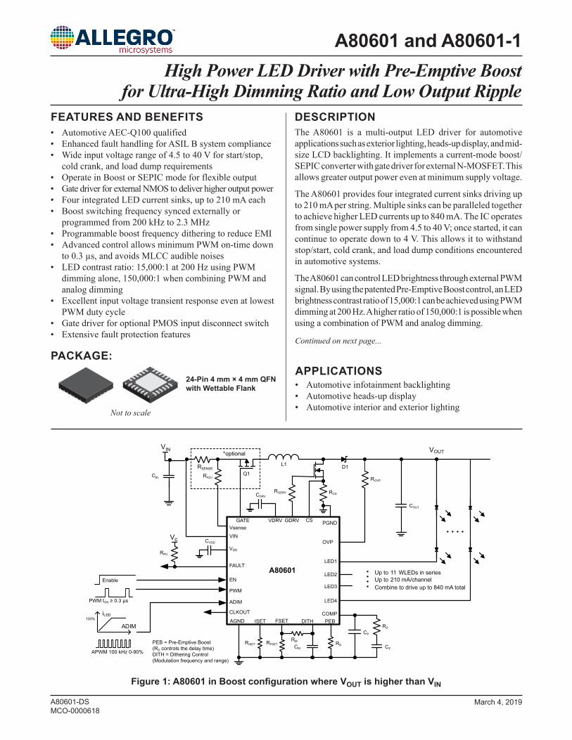
The A80601 is a multi-output LED driver for automotive applications such as exterior lighting, heads-up display, and mid-size LCD backlighting. It implements a current-mode boost/SEPIC converter with gate driver for external N-MOSFET. This allows greater output power even at minimum supply voltage.
The A80601 provides four integrated current sinks driving up to 210 mA per string. Multiple sinks can be paralleled together to achieve higher LED currents up to 840 mA. The IC operates from single power supply from 4.5 to 40 V; once started, it can continue to operate down to 4 V. This allows it to withstand stop/start, cold crank, and load dump conditions encountered in automotive systems.
The A80601 can control LED brightness through external PWM signal. By using the patented Pre-Emptive Boost control, an LED brightness contrast ratio of 15,000:1 can be achieved using PWM dimming at 200 Hz. A higher ratio of 150,000:1 is possible when using a combination of PWM and analog dimming.
A80601-DSMCO-0000618
• Automotive AEC-Q100 qualified• Enhanced fault handling for ASIL B system compliance• Wide input voltage range of 4.5 to 40 V for start/stop,
cold crank, and load dump requirements• Operate in Boost or SEPIC mode for flexible output• Gate driver for external NMOS to deliver higher output power• Four integrated LED current sinks, up to 210 mA each• Boost switching frequency synced externally or
programmed from 200 kHz to 2.3 MHz• Programmable boost frequency dithering to reduce EMI• Advanced control allows minimum PWM on-time down
to 0.3 µs, and avoids MLCC audible noises• LED contrast ratio: 15,000:1 at 200 Hz using PWM
dimming alone, 150,000:1 when combining PWM and analog dimming
• Excellent input voltage transient response even at lowest PWM duty cycle
• Gate driver for optional PMOS input disconnect switch• Extensive fault protection features
High Power LED Driver with Pre-Emptive Boost for Ultra-High Dimming Ratio and Low Output Ripple
PACKAGE:
Figure 1: A80601 in Boost configuration where VOUT is higher than VIN
Not to scale
A80601 and A80601-1
Continued on next page...
FEATURES AND BENEFITS DESCRIPTION
March 4, 2019
A80601
PGND
Q1
VIN
VDD
GATE
LED1
LED4
Vsense
PWM
ADIM
FAULT
Vc
CS
COMPISET
OVP
AGND
RSENSE
RISET CZ
RZ
CP
RPU
ROVP
L1
VIN*optional VOUT
LED2
LED3
RFSET
FSET
CLKOUT
Up to 11 WLEDs in seriesUp to 210 mA/channel
PWM tON ≥ 0.3 µs
CVDD
Cin
ENEnable
DITH PEB
CMRD
RM
APWM 100 kHz 0-90%
COUT
VDRV GDRV
PEB = Pre-Emptive Boost(RD controls the delay time)DITH = Dithering Control(Modulation frequency and range)
Combine to drive up to 840 mA total
CDRV
ADIM
iLED100%
D1
RGDRV RCS
RADJ
• Automotive infotainment backlighting• Automotive heads-up display• Automotive interior and exterior lighting
APPLICATIONS24-Pin 4 mm × 4 mm QFN with Wettable Flank
High Power LED Driver with Pre-Emptive Boost for Ultra-High Dimming Ratio and Low Output Ripple
A80601 and A80601-1
2Allegro MicroSystems, LLC 955 Perimeter Road Manchester, NH 03103-3353 U.S.A.www.allegromicro.com
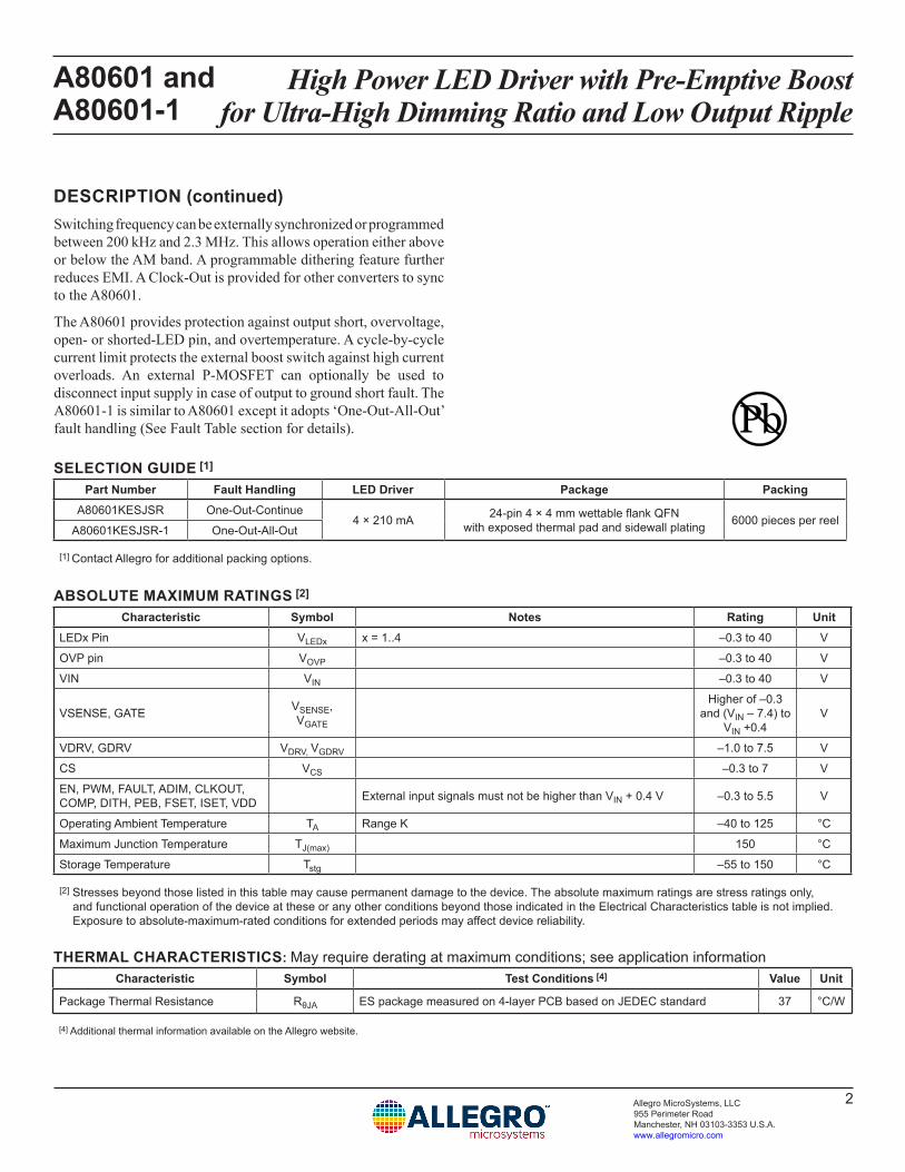
ABSOLUTE MAXIMUM RATINGS [2]
Characteristic Symbol Notes Rating UnitLEDx Pin VLEDx x = 1..4 –0.3 to 40 V
OVP pin VOVP –0.3 to 40 V
VIN VIN –0.3 to 40 V
VSENSE, GATE VSENSE, VGATE
Higher of –0.3 and (VIN – 7.4) to
VIN +0.4V
VDRV, GDRV VDRV, VGDRV –1.0 to 7.5 V
CS VCS –0.3 to 7 V
EN, PWM, FAULT, ADIM, CLKOUT, COMP, DITH, PEB, FSET, ISET, VDD External input signals must not be higher than VIN + 0.4 V –0.3 to 5.5 V
Operating Ambient Temperature TA Range K –40 to 125 °C
Maximum Junction Temperature TJ(max) 150 °C
Storage Temperature Tstg –55 to 150 °C
[2] Stresses beyond those listed in this table may cause permanent damage to the device. The absolute maximum ratings are stress ratings only, and functional operation of the device at these or any other conditions beyond those indicated in the Electrical Characteristics table is not implied. Exposure to absolute-maximum-rated conditions for extended periods may affect device reliability.
SELECTION GUIDE [1]
Part Number Fault Handling LED Driver Package PackingA80601KESJSR One-Out-Continue
4 × 210 mA 24-pin 4 × 4 mm wettable flank QFN with exposed thermal pad and sidewall plating 6000 pieces per reel
A80601KESJSR-1 One-Out-All-Out
[1] Contact Allegro for additional packing options.
THERMAL CHARACTERISTICS: May require derating at maximum conditions; see application informationCharacteristic Symbol Test Conditions [4] Value Unit
Package Thermal Resistance RθJA ES package measured on 4-layer PCB based on JEDEC standard 37 °C/W
[4] Additional thermal information available on the Allegro website.
DESCRIPTION (continued)Switching frequency can be externally synchronized or programmed between 200 kHz and 2.3 MHz. This allows operation either above or below the AM band. A programmable dithering feature further reduces EMI. A Clock-Out is provided for other converters to sync to the A80601.
The A80601 provides protection against output short, overvoltage, open- or shorted-LED pin, and overtemperature. A cycle-by-cycle current limit protects the external boost switch against high current overloads. An external P-MOSFET can optionally be used to disconnect input supply in case of output to ground short fault. The A80601-1 is similar to A80601 except it adopts ‘One-Out-All-Out’ fault handling (See Fault Table section for details).
High Power LED Driver with Pre-Emptive Boost for Ultra-High Dimming Ratio and Low Output Ripple
A80601 and A80601-1
3Allegro MicroSystems, LLC 955 Perimeter Road Manchester, NH 03103-3353 U.S.A.www.allegromicro.com
Table of ContentsFeatures and Benefits ........................................................... 1Description .......................................................................... 1Applications ......................................................................... 1Package ............................................................................. 1Selection Guide ................................................................... 2Absolute Maximum Ratings ................................................... 2Thermal Characteristics ........................................................ 2Typical Application – SEPIC .................................................. 3Functional Block Diagram ..................................................... 4Pinout Diagram and Terminal List ........................................... 5Electrical Characteristics ....................................................... 6Functional Description .........................................................11
Enabling the IC ................................................................11Powering Up: LED Detection Phase .................................. 12Powering Up: Boost Output Undervoltage .......................... 14Soft Start Function .......................................................... 14Frequency Selection ........................................................ 15Synchronization .............................................................. 15Loss of External Sync Signal ............................................ 16Switching Frequency Dithering ......................................... 17Clock Out Function.......................................................... 17
LED Current Setting ........................................................ 18PWM Dimming ............................................................... 18Pre-Emptive Boost (PEB) ................................................. 19Analog Dimming ............................................................. 20
ADIM Mode ................................................................ 20APWM Mode .............................................................. 21
Extending LED Dimming Ratio.......................................... 22Analog Dimming with External Voltage............................... 23VDD .............................................................................. 24VDRV ............................................................................ 24Shutdown....................................................................... 24
Fault Detection and Protection ............................................. 25FAULT Status ................................................................. 25LED String Partial-Short Detect ........................................ 27Overvoltage Protection .................................................... 28Boost Switch Overcurrent Protection ................................. 29Input Overcurrent Protection and Disconnect Switch ........... 30Setting the Input Current Sense Resistor ........................... 31Input UVLO .................................................................... 31Fault Protection During Operation ..................................... 31
Package Outline Drawing .................................................... 34Appendix: External MOSFET Selection Guide ....................... 35
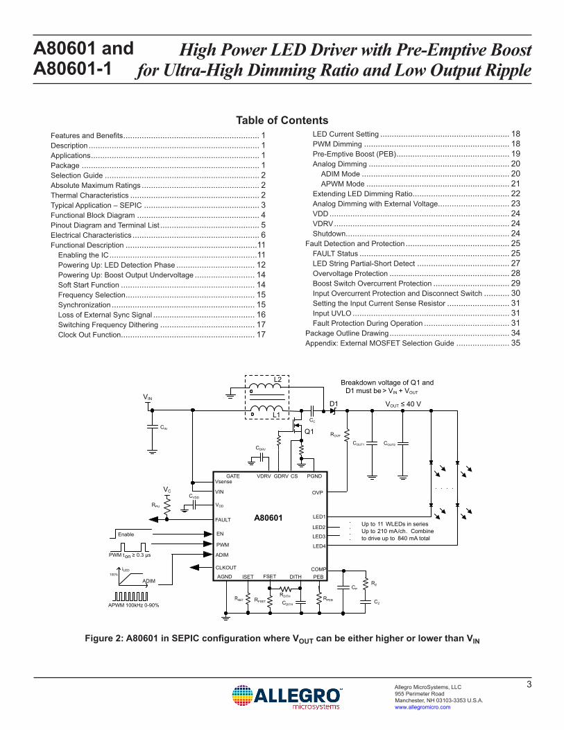
Figure 2: A80601 in SEPIC configuration where VOUT can be either higher or lower than VIN
OVPVIN
VDD
GATE
LED1
LED4
Vsense
ADIM
FAULT
VC
GDRV PGND
RPU
CDRV
CIN
COUT1 COUT2
ROVP
VIN
Breakdown voltage of Q1 and D1 must be > VIN + VOUT
LED2
LED3
CS
CVDD
VDRV
L1CC
L2
D1
Q1
Up to 11 WLEDs in seriesUp to 210 mA/ch. Combine to drive up to 840 mA total
A80601
PWM
PWM ton ≥ 0.3 µs
ENEnable
COMPISETAGND
RISET CZ
RZCP
RFSET
FSET
CLKOUT
DITH PEB
CDITH
RPEBRDITH
VOUT ≤ 40 V
APWM 100kHz 0-90%
ADIM
iLED100%
High Power LED Driver with Pre-Emptive Boost for Ultra-High Dimming Ratio and Low Output Ripple
A80601 and A80601-1
4Allegro MicroSystems, LLC 955 Perimeter Road Manchester, NH 03103-3353 U.S.A.www.allegromicro.com
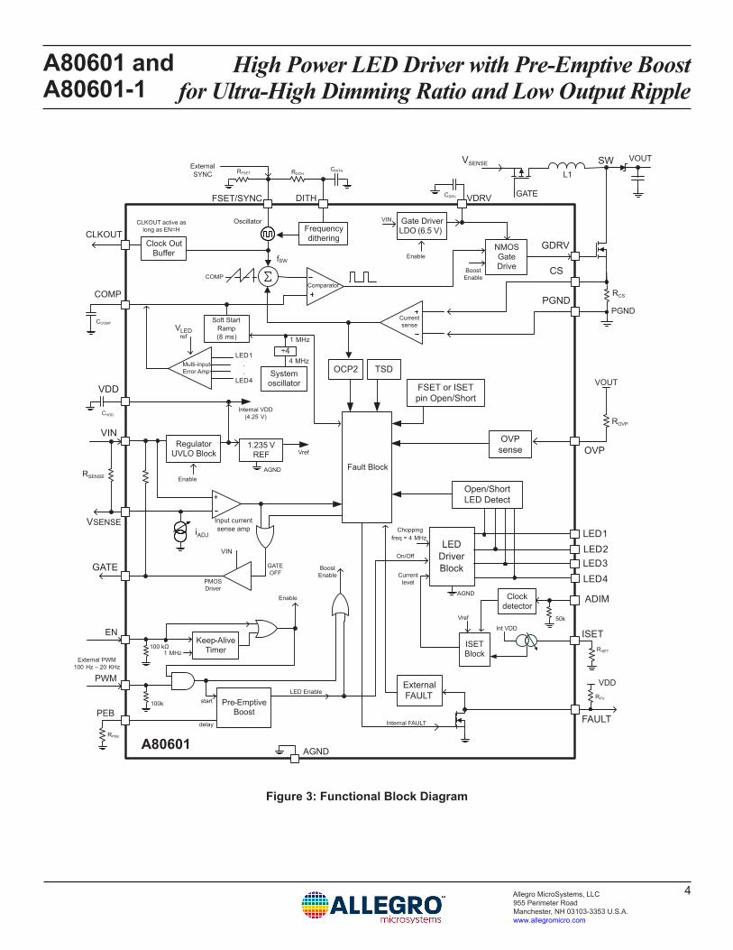
Figure 3: Functional Block Diagram
Fault Block
PMOS Driver
Current sense
LED Driver Block
TSD
Open/Short LED Detect
Regulator UVLO Block
ISET
FAULT
VDD
VIN
GATE
GDRV
VSENSE
AGND
COMP
Input current sense amp
1.235 V REF
NMOSGate Drive
PGND
Oscillator
Internal VDD(4.25 V)
Vref
OVP
LED1
LED4
Vref
AGND
ISET Block
Int VDD
GATE OFF
ADIM
+
iADJ
OVP sense
OCP2
FSET or ISET pin Open/Short
VIN
FSET/SYNC
LED3LED2
A80601
ComparatorCOMP
SW
RCS
L1
PGND
CS
CDRV VDRV
CVDD
Multi-input Error Amp
LED1..
LED4
VLEDref
CCOMP
Enable
VOUT
VOUTVSENSE
GATE
ROVP
RISET
VDDRPU
RSENSE
Boost Enable
Boost Enable
External FAULT
Internal FAULT
External SYNC
AGND
On/Off
Current level
EN
Enable
PEB
RPEB
External PWM100 Hz – 20 KHz
PWM
Gate Driver LDO (6.5 V)
Enable
VINFrequency dithering
DITH
RDITHCDITH
Clock Out Buffer
CLKOUTCLKOUT active as
long as EN=H
Keep-Alive Timer
Pre-Emptive Boost
100 kΩ
LED Enable
100k
delay
start
Clock detector
Soft Start Ramp(8 ms)
System oscillator
4 MHz÷4
1 MHz
Chopping freq = 4 MHz
fSW
1 MHz
50k
RFSET
High Power LED Driver with Pre-Emptive Boost for Ultra-High Dimming Ratio and Low Output Ripple
A80601 and A80601-1
5Allegro MicroSystems, LLC 955 Perimeter Road Manchester, NH 03103-3353 U.S.A.www.allegromicro.com
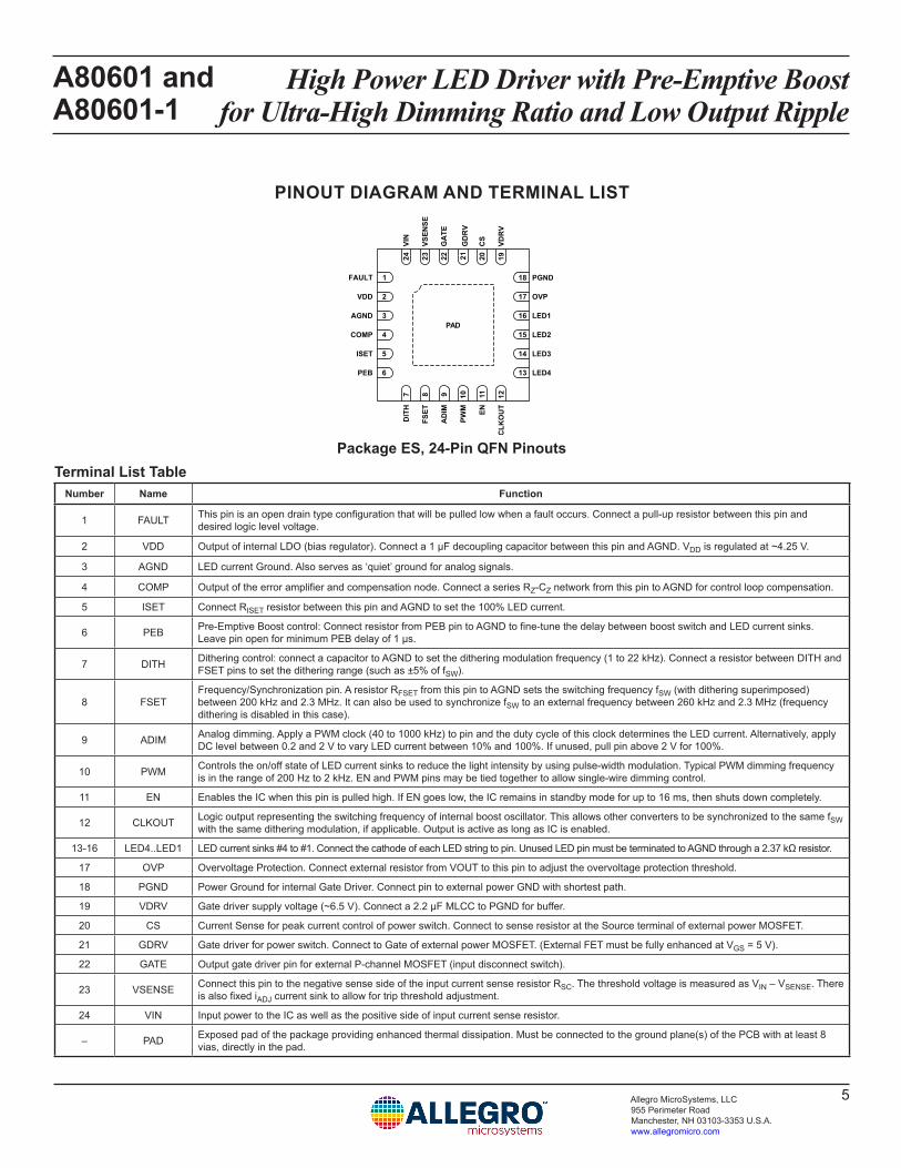
PINOUT DIAGRAM AND TERMINAL LIST
Package ES, 24-Pin QFN Pinouts
1
AGND
2
COMP
3
ISET
4
DITH
5
FSET
6
ADIM
7
PWM
8
EN
9
CLKOUT
10
PEB
11
LED4
12
LED3
13
LED2
14
LED1
15
OVP
16
PGND
17
VDRV
18
CS
19
GDRV
20
GATE
21
VSENSE
22
VIN
23
FAULT
24
VDD
PAD
Terminal List TableNumber Name Function
1 FAULT This pin is an open drain type configuration that will be pulled low when a fault occurs. Connect a pull-up resistor between this pin and desired logic level voltage.
2 VDD Output of internal LDO (bias regulator). Connect a 1 µF decoupling capacitor between this pin and AGND. VDD is regulated at ~4.25 V.
3 AGND LED current Ground. Also serves as ‘quiet’ ground for analog signals.
4 COMP Output of the error amplifier and compensation node. Connect a series RZ-CZ network from this pin to AGND for control loop compensation.
5 ISET Connect RISET resistor between this pin and AGND to set the 100% LED current.
6 PEB Pre-Emptive Boost control: Connect resistor from PEB pin to AGND to fine-tune the delay between boost switch and LED current sinks. Leave pin open for minimum PEB delay of 1 μs.
7 DITH Dithering control: connect a capacitor to AGND to set the dithering modulation frequency (1 to 22 kHz). Connect a resistor between DITH and FSET pins to set the dithering range (such as ±5% of fSW).
8 FSETFrequency/Synchronization pin. A resistor RFSET from this pin to AGND sets the switching frequency fSW (with dithering superimposed) between 200 kHz and 2.3 MHz. It can also be used to synchronize fSW to an external frequency between 260 kHz and 2.3 MHz (frequency dithering is disabled in this case).
9 ADIM Analog dimming. Apply a PWM clock (40 to 1000 kHz) to pin and the duty cycle of this clock determines the LED current. Alternatively, apply DC level between 0.2 and 2 V to vary LED current between 10% and 100%. If unused, pull pin above 2 V for 100%.
10 PWM Controls the on/off state of LED current sinks to reduce the light intensity by using pulse-width modulation. Typical PWM dimming frequency is in the range of 200 Hz to 2 kHz. EN and PWM pins may be tied together to allow single-wire dimming control.
11 EN Enables the IC when this pin is pulled high. If EN goes low, the IC remains in standby mode for up to 16 ms, then shuts down completely.
12 CLKOUT Logic output representing the switching frequency of internal boost oscillator. This allows other converters to be synchronized to the same fSW with the same dithering modulation, if applicable. Output is active as long as IC is enabled.
13-16 LED4..LED1 LED current sinks #4 to #1. Connect the cathode of each LED string to pin. Unused LED pin must be terminated to AGND through a 2.37 kΩ resistor.
17 OVP Overvoltage Protection. Connect external resistor from VOUT to this pin to adjust the overvoltage protection threshold.
18 PGND Power Ground for internal Gate Driver. Connect pin to external power GND with shortest path.
19 VDRV Gate driver supply voltage (~6.5 V). Connect a 2.2 µF MLCC to PGND for buffer.
20 CS Current Sense for peak current control of power switch. Connect to sense resistor at the Source terminal of external power MOSFET.
21 GDRV Gate driver for power switch. Connect to Gate of external power MOSFET. (External FET must be fully enhanced at VGS = 5 V).
22 GATE Output gate driver pin for external P-channel MOSFET (input disconnect switch).
23 VSENSE Connect this pin to the negative sense side of the input current sense resistor RSC. The threshold voltage is measured as VIN – VSENSE. There is also fixed iADJ current sink to allow for trip threshold adjustment.
24 VIN Input power to the IC as well as the positive side of input current sense resistor.
– PAD Exposed pad of the package providing enhanced thermal dissipation. Must be connected to the ground plane(s) of the PCB with at least 8 vias, directly in the pad.
High Power LED Driver with Pre-Emptive Boost for Ultra-High Dimming Ratio and Low Output Ripple
A80601 and A80601-1
6Allegro MicroSystems, LLC 955 Perimeter Road Manchester, NH 03103-3353 U.S.A.www.allegromicro.com
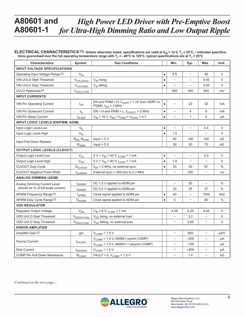
Characteristics Symbol Test Conditions Min. Typ. Max. UnitINPUT VOLTAGE SPECIFICATIONSOperating Input Voltage Range [3] VIN 4.5 − 40 V
VIN UVLO Start Threshold VUVLO(rise) VIN rising − – 4.45 V
VIN UVLO Stop Threshold VUVLO(fall) VIN falling − – 4.05 V
UVLO Hysteresis [2] VUVLO_HYS 300 400 500 mV
INPUT CURRENTS
VIN Pin Operating Current IOPEN and PWM = H, CGATE = 1 nF from GDRV to PGND, fSW = 2 MHz − 22 32 mA
VIN Pin Quiescent Current IQ EN = H and PWM = L, fCLKOUT = 2 MHz − 4 6 mA
VIN Pin Sleep Current ISLEEP VIN = 16 V, VEN / VPWM = VSYNC = 0 V − 1 5 µA
INPUT LOGIC LEVELS (EN/PWM, ADIM)Input Logic Level-Low VIL − − 0.4 V
Input Logic Level-High VIH 1.5 − − V
Input Pull-Down ResistorREN, RPWM Input = 5 V 60 100 140 kΩ
RADIM Input = 5 V 30 50 70 kΩ
OUTPUT LOGIC LEVELS (CLKOUT)Output Logic Level-Low VOL 5 V < VIN < 40 V, iLOAD = 1 mA − − 0.3 V
Output Logic Level-High VOH 5 V < VIN < 40 V, iLOAD = 1 mA 1.8 − − V
CLKOUT Duty Cycle DCLKOUT fSW = 2 MHz, no external sync 33 50 67 %
CLKOUT Negative Pulse Width tCLKNPW External sync = 260 kHz to 2.3 MHz − 200 − ns
ANALOG DIMMING (ADIM)
Analog Dimming Current Level (shown as % of full-scale current)
iADIM50 DC 1.0 V applied to ADIM pin − 50 − %
iADIM25 DC 0.5 V applied to ADIM pin 23 25 27 %
APWM Frequency Range [2] fAPWM Clock signal applied to ADIM pin 40 − 1000 kHz
APWM Duty Cycle Range [2] DAPWM Clock signal applied to ADIM pin 0 − 90 %
VDD REGULATORRegulator Output Voltage VDD VIN > 6 V, iLOAD < 1 mA 4.05 4.25 4.45 V
VDD UVLO Start Threshold VDDUVLOrise VDD rising, no external load − 3.2 − V
VDD UVLO Stop Threshold VDDUVLOfall VDD falling, no external load − 2.65 − V
ERROR AMPLIFIERAmplifier Gain [2] gm VCOMP = 1.5 V − 900 − μA/V
Source Current IEA(SRC)VCOMP = 1.5 V, A80601 (symm COMP) − –500 − μA
VCOMP = 1.5 V, A80601-1 (asymm COMP) − –700 − μA
Sink Current IEA(SINK) VCOMP = 1.5 V − +500 − μA
COMP Pin Pull Down Resistance RCOMP FAULT = 0, VCOMP = 1.5 V − 1.4 − kΩ
ELECTRICAL CHARACTERISTICS [1]: Unless otherwise noted, specifications are valid at VIN = 12 V, TJ = 25°C, • indicates specifica-tions guaranteed over the full operating temperature range with TJ = –40°C to 125°C, typical specifications are at TJ = 25°C
Continued on the next page…
High Power LED Driver with Pre-Emptive Boost for Ultra-High Dimming Ratio and Low Output Ripple
A80601 and A80601-1
7Allegro MicroSystems, LLC 955 Perimeter Road Manchester, NH 03103-3353 U.S.A.www.allegromicro.com
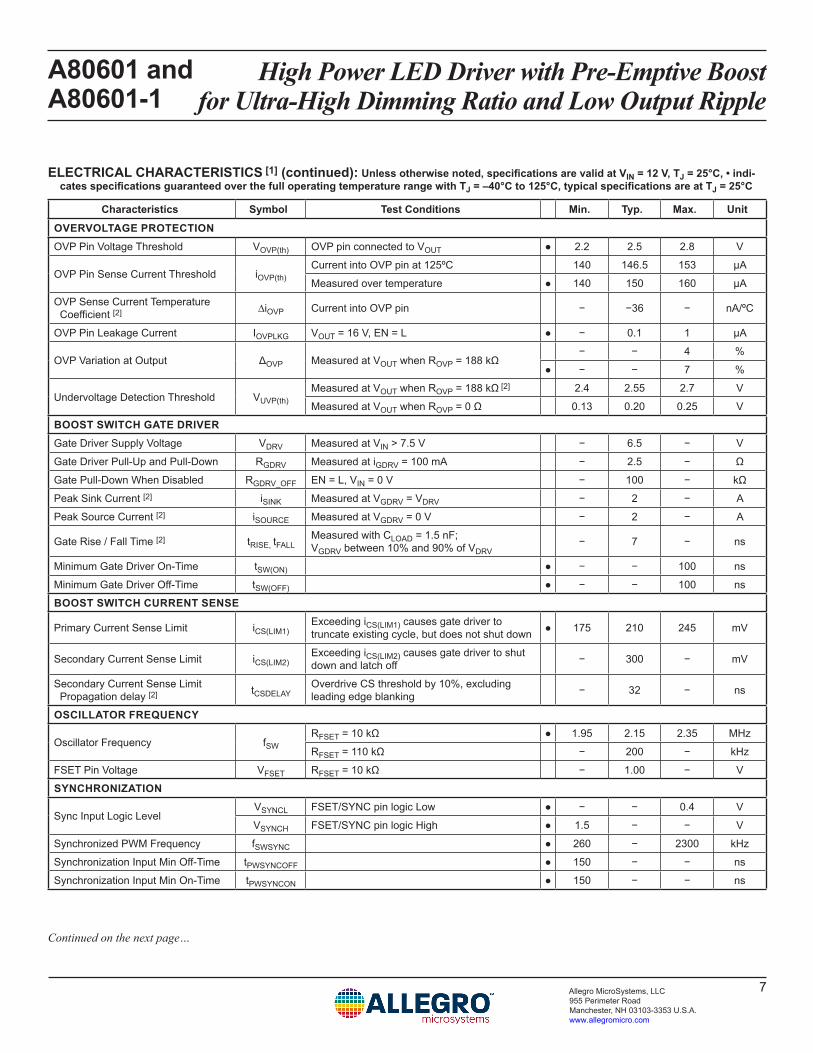
Characteristics Symbol Test Conditions Min. Typ. Max. UnitOVERVOLTAGE PROTECTIONOVP Pin Voltage Threshold VOVP(th) OVP pin connected to VOUT 2.2 2.5 2.8 V
OVP Pin Sense Current Threshold iOVP(th)Current into OVP pin at 125ºC 140 146.5 153 µA
Measured over temperature 140 150 160 µA
OVP Sense Current Temperature Coefficient [2] ∆iOVP Current into OVP pin − −36 − nA/ºC
OVP Pin Leakage Current IOVPLKG VOUT = 16 V, EN = L − 0.1 1 µA
OVP Variation at Output ΔOVP Measured at VOUT when ROVP = 188 kΩ− − 4 %
− − 7 %
Undervoltage Detection Threshold VUVP(th)Measured at VOUT when ROVP = 188 kΩ [2] 2.4 2.55 2.7 V
Measured at VOUT when ROVP = 0 Ω 0.13 0.20 0.25 V
BOOST SWITCH GATE DRIVERGate Driver Supply Voltage VDRV Measured at VIN > 7.5 V − 6.5 − V
Gate Driver Pull-Up and Pull-Down RGDRV Measured at iGDRV = 100 mA − 2.5 − Ω
Gate Pull-Down When Disabled RGDRV_OFF EN = L, VIN = 0 V − 100 − kΩ
Peak Sink Current [2] iSINK Measured at VGDRV = VDRV − 2 − A
Peak Source Current [2] iSOURCE Measured at VGDRV = 0 V − 2 − A
Gate Rise / Fall Time [2] tRISE, tFALLMeasured with CLOAD = 1.5 nF; VGDRV between 10% and 90% of VDRV
− 7 − ns
Minimum Gate Driver On-Time tSW(ON) − − 100 ns
Minimum Gate Driver Off-Time tSW(OFF) − − 100 ns
BOOST SWITCH CURRENT SENSE
Primary Current Sense Limit iCS(LIM1)Exceeding iCS(LIM1) causes gate driver to truncate existing cycle, but does not shut down 175 210 245 mV
Secondary Current Sense Limit iCS(LIM2)Exceeding iCS(LIM2) causes gate driver to shut down and latch off − 300 − mV
Secondary Current Sense Limit Propagation delay [2] tCSDELAY
Overdrive CS threshold by 10%, excluding leading edge blanking − 32 − ns
OSCILLATOR FREQUENCY
Oscillator Frequency fSWRFSET = 10 kΩ 1.95 2.15 2.35 MHz
RFSET = 110 kΩ − 200 − kHz
FSET Pin Voltage VFSET RFSET = 10 kΩ − 1.00 − V
SYNCHRONIZATION
Sync Input Logic LevelVSYNCL FSET/SYNC pin logic Low − − 0.4 V
VSYNCH FSET/SYNC pin logic High 1.5 − − V
Synchronized PWM Frequency fSWSYNC 260 − 2300 kHz
Synchronization Input Min Off-Time tPWSYNCOFF 150 − − ns
Synchronization Input Min On-Time tPWSYNCON 150 − − ns
ELECTRICAL CHARACTERISTICS [1] (continued): Unless otherwise noted, specifications are valid at VIN = 12 V, TJ = 25°C, • indi-cates specifications guaranteed over the full operating temperature range with TJ = –40°C to 125°C, typical specifications are at TJ = 25°C
Continued on the next page…
High Power LED Driver with Pre-Emptive Boost for Ultra-High Dimming Ratio and Low Output Ripple
A80601 and A80601-1
8Allegro MicroSystems, LLC 955 Perimeter Road Manchester, NH 03103-3353 U.S.A.www.allegromicro.com
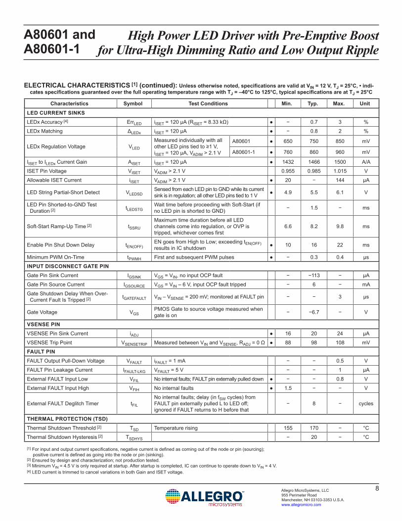
Characteristics Symbol Test Conditions Min. Typ. Max. UnitLED CURRENT SINKSLEDx Accuracy [4] ErrLED iISET = 120 µA (RISET = 8.33 kΩ) − 0.7 3 %
LEDx Matching ΔLEDx iISET = 120 µA − 0.8 2 %
LEDx Regulation Voltage VLED
Measured individually with all other LED pins tied to ≥1 V, iISET = 120 µA, VADIM > 2.1 V
A80601 650 750 850 mV
A80601-1 760 860 960 mV
IISET to ILEDx Current Gain AISET iISET = 120 µA 1432 1466 1500 A/A
ISET Pin Voltage VISET VADIM > 2.1 V 0.955 0.985 1.015 V
Allowable ISET Current iISET VADIM > 2.1 V 20 − 144 µA
LED String Partial-Short Detect VLEDSDSensed from each LED pin to GND while its current sink is in regulation; all other LED pins tied to 1 V 4.9 5.5 6.1 V
LED Pin Shorted-to-GND Test Duration [2] tLEDSTG
Wait time before proceeding with Soft-Start (if no LED pin is shorted to GND) − 1.5 − ms
Soft-Start Ramp-Up Time [2] tSSRU
Maximum time duration before all LED channels come into regulation, or OVP is tripped, whichever comes first
6.6 8.2 9.8 ms
Enable Pin Shut Down Delay tEN(OFF)EN goes from High to Low; exceeding tEN(OFF) results in IC shutdown 10 16 22 ms
Minimum PWM On-Time tPWMH First and subsequent PWM pulses − 0.3 0.4 µs
INPUT DISCONNECT GATE PINGate Pin Sink Current IGSINK VGS = VIN, no input OCP fault − −113 − µA
Gate Pin Source Current IGSOURCE VGS = VIN – 6 V, input OCP fault tripped − 6 − mA
Gate Shutdown Delay When Over-Current Fault Is Tripped [2] tGATEFAULT VIN – VSENSE = 200 mV; monitored at FAULT pin − − 3 µs
Gate Voltage VGSPMOS Gate to source voltage measured when gate is on − −6.7 − V
VSENSE PINVSENSE Pin Sink Current iADJ 16 20 24 µA
VSENSE Trip Point VSENSETRIP Measured between VIN and VSENSE, RADJ = 0 Ω 88 98 108 mV
FAULT PINFAULT Output Pull-Down Voltage VFAULT iFAULT = 1 mA − − 0.5 V
FAULT Pin Leakage Current IFAULT-LKG VFAULT = 5 V − − 1 µA
External FAULT Input Low VFIL No internal faults; FAULT pin externally pulled down − − 0.8 V
External FAULT Input High VFIH No internal faults 1.5 − − V
External FAULT Deglitch Timer tFIL
No internal faults; delay (in fSW cycles) from FAULT pin externally pulled L to LED off; ignored if FAULT returns to H before that
− 8 − cycles
THERMAL PROTECTION (TSD)Thermal Shutdown Threshold [2] TSD Temperature rising 155 170 − °C
Thermal Shutdown Hysteresis [2] TSDHYS − 20 − °C
[1] For input and output current specifications, negative current is defined as coming out of the node or pin (sourcing); positive current is defined as going into the node or pin (sinking).
[2] Ensured by design and characterization; not production tested.[3] Minimum VIN = 4.5 V is only required at startup. After startup is completed, IC can continue to operate down to VIN = 4 V.[4] LED current is trimmed to cancel variations in both Gain and ISET voltage.
ELECTRICAL CHARACTERISTICS [1] (continued): Unless otherwise noted, specifications are valid at VIN = 12 V, TJ = 25°C, • indi-cates specifications guaranteed over the full operating temperature range with TJ = –40°C to 125°C, typical specifications are at TJ = 25°C
High Power LED Driver with Pre-Emptive Boost for Ultra-High Dimming Ratio and Low Output Ripple
A80601 and A80601-1
9Allegro MicroSystems, LLC 955 Perimeter Road Manchester, NH 03103-3353 U.S.A.www.allegromicro.com
APPLICATION EXAMPLES
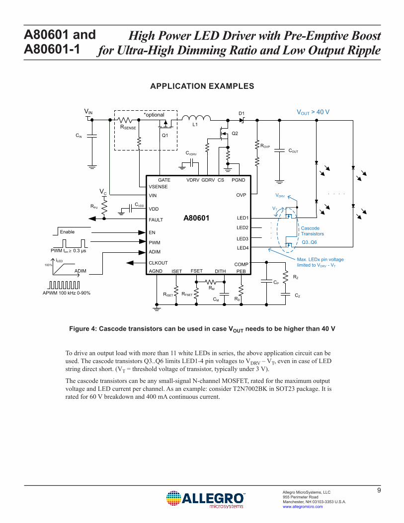
Figure 4: Cascode transistors can be used in case VOUT needs to be higher than 40 V
Q1
VC
RSENSE
RPU
CVDRV
CIN
COUT
ROVP
L1
VIN *optional VOUT > 40 V
CVDD
OVPVIN
VDD
GATE
LED1
LED4
VSENSE
ADIM
FAULT
GDRV PGND
LED2
LED3
CSVDRV
A80601
PWM
EN
PWM ton ≥ 0.3 µs
Enable
APWM 100 kHz 0-90%
ADIM
iLED100%
VDRV
Max. LEDx pin voltage limited to VDRV - VT
VT
Cascode Transistors
CP
RISET CZ
RZ
RFSETRD
COMPISETAGND FSET
CLKOUT
DITH PEB
CM
RM
D1
Q2
Q3..Q6
To drive an output load with more than 11 white LEDs in series, the above application circuit can be used. The cascode transistors Q3..Q6 limits LED1-4 pin voltages to VDRV – VT, even in case of LED string direct short. (VT = threshold voltage of transistor, typically under 3 V).
The cascode transistors can be any small-signal N-channel MOSFET, rated for the maximum output voltage and LED current per channel. As an example: consider T2N7002BK in SOT23 package. It is rated for 60 V breakdown and 400 mA continuous current.
High Power LED Driver with Pre-Emptive Boost for Ultra-High Dimming Ratio and Low Output Ripple
A80601 and A80601-1
10Allegro MicroSystems, LLC 955 Perimeter Road Manchester, NH 03103-3353 U.S.A.www.allegromicro.com
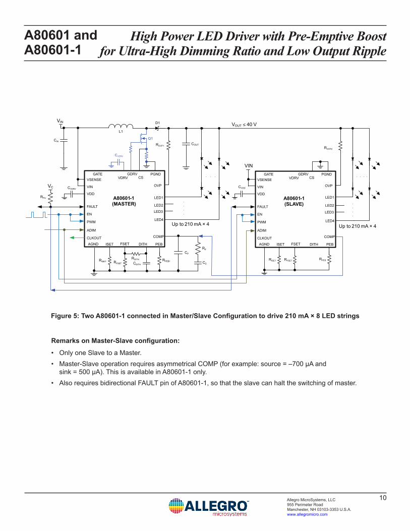
Figure 5: Two A80601-1 connected in Master/Slave Configuration to drive 210 mA × 8 LED strings
Remarks on Master-Slave configuration:
• Only one Slave to a Master.• Master-Slave operation requires asymmetrical COMP (for example: source = –700 µA and
sink = 500 µA). This is available in A80601-1 only.• Also requires bidirectional FAULT pin of A80601-1, so that the slave can halt the switching of master.
OVPVIN
VDD
GATE
LED1
LED4
VSENSE
ADIM
FAULT
VC
GDRV PGND
RPU
CVDRV
CIN
ROVP1
L1
VIN VOUT ≤ 40 V
LED2
LED3
CS
CVDRV
VDRV
COUT
VIN
A80601-1(MASTER)
CP
COMP
CZ
RZ
ROVP2
PWM
EN
ISETAGND
RISET RFSET
FSET DITH PEB
CDITH
RPEB1RDITH
CLKOUT
OVPVIN
VDD
GATE
LED1
LED4
VSENSE
ADIM
FAULT
GDRV PGND
LED2
LED3
CSVDRV
A80601-1(SLAVE)
COMP
PWM
EN
ISETAGND FSET DITH PEB
CLKOUT
RISET RFSET RPEB
CVDD
Up to 210 mA × 4 Up to 210 mA × 4
D1
Q1
High Power LED Driver with Pre-Emptive Boost for Ultra-High Dimming Ratio and Low Output Ripple
A80601 and A80601-1
11Allegro MicroSystems, LLC 955 Perimeter Road Manchester, NH 03103-3353 U.S.A.www.allegromicro.com
FUNCTIONAL DESCRIPTION
The A80601 is a multi-string LED regulator with four preci-sion current sinks and a gate driver for external boost MOSFET switch. It incorporates a patented Pre-Emptive Boost (PEB) control algorithm to achieve PWM dimming ratio over 15,000:1 at 200 Hz. PEB control also minimizes output ripple to avoid audible noise from output ceramic capacitors.
The switching frequency can be either synchronized to an external clock or generated internally. Spread-spectrum tech-nique (with user-programmable dithering range and modulation frequency) is provided to reduce EMI. A clock-out signal (CLK-OUT) allows other converters to be synchronized to the switching frequency of A80601.
Enabling the IC The A80601 wakes up when EN pin is pulled above logic high level, provided that VIN pin voltage is over the VIN_UVLO threshold. The boost stage and LED channels are enabled sepa-rately by PWM = H signal after the IC powers up.
The IC performs a series of safety checks at power up, to deter-mine if there are possible fault conditions that might prevent the system from functioning correctly. Power-up checks include:
• VOUT shorted to GND• LED pin shorted to GND• FSET pin open/shorted• ISET pin open/shorted to GND, etc.
Only if no faults were detected, then the IC can proceed to start switching.
As long as EN = H, the PWM pin can be toggled to control the brightness of LED channels by using PWM dimming. Alterna-tively, EN and PWM can be tied together to allow single-wire control for both power on/off and PWM dimming. If EN is pulled low for longer than 16 ms, the IC shuts off.
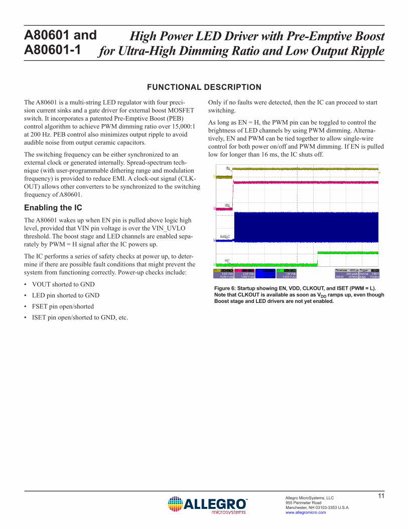
Figure 6: Startup showing EN, VDD, CLKOUT, and ISET (PWM = L). Note that CLKOUT is available as soon as VDD ramps up, even though Boost stage and LED drivers are not yet enabled.
High Power LED Driver with Pre-Emptive Boost for Ultra-High Dimming Ratio and Low Output Ripple
A80601 and A80601-1
12Allegro MicroSystems, LLC 955 Perimeter Road Manchester, NH 03103-3353 U.S.A.www.allegromicro.com
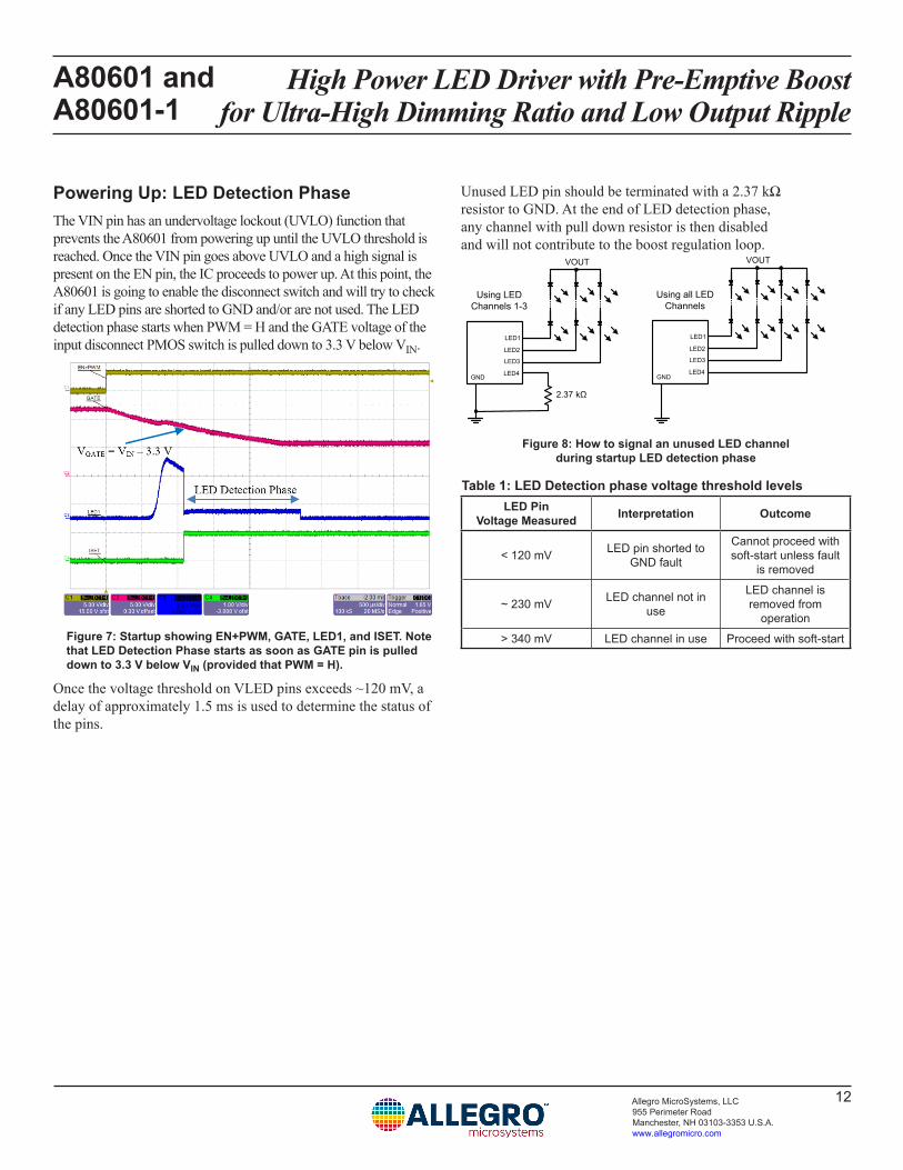
Powering Up: LED Detection Phase The VIN pin has an undervoltage lockout (UVLO) function that prevents the A80601 from powering up until the UVLO threshold is reached. Once the VIN pin goes above UVLO and a high signal is present on the EN pin, the IC proceeds to power up. At this point, the A80601 is going to enable the disconnect switch and will try to check if any LED pins are shorted to GND and/or are not used. The LED detection phase starts when PWM = H and the GATE voltage of the input disconnect PMOS switch is pulled down to 3.3 V below VIN.
Figure 7: Startup showing EN+PWM, GATE, LED1, and ISET. Note that LED Detection Phase starts as soon as GATE pin is pulled down to 3.3 V below VIN (provided that PWM = H).
Once the voltage threshold on VLED pins exceeds ~120 mV, a delay of approximately 1.5 ms is used to determine the status of the pins.
Unused LED pin should be terminated with a 2.37 kΩ resistor to GND. At the end of LED detection phase, any channel with pull down resistor is then disabled and will not contribute to the boost regulation loop.
LED3
LED4GND
VOUT
2.37 kΩ
Using LED Channels 1-3
LED1
LED2
GND
Using all LED Channels
VOUT
LED3
LED4
LED1
LED2
Figure 8: How to signal an unused LED channel during startup LED detection phase
Table 1: LED Detection phase voltage threshold levelsLED Pin
Voltage Measured Interpretation Outcome
< 120 mV LED pin shorted to GND fault
Cannot proceed with soft-start unless fault
is removed
~ 230 mV LED channel not in use
LED channel is removed from
operation
> 340 mV LED channel in use Proceed with soft-start
High Power LED Driver with Pre-Emptive Boost for Ultra-High Dimming Ratio and Low Output Ripple
A80601 and A80601-1
13Allegro MicroSystems, LLC 955 Perimeter Road Manchester, NH 03103-3353 U.S.A.www.allegromicro.com
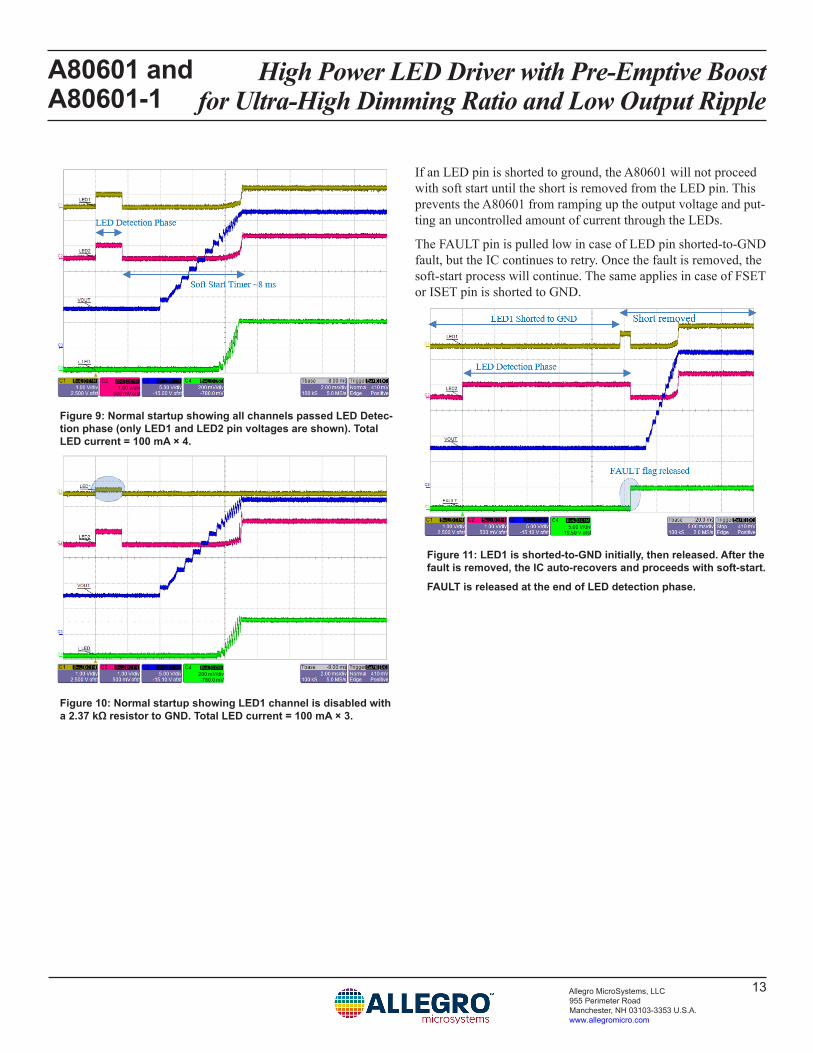
Figure 9: Normal startup showing all channels passed LED Detec-tion phase (only LED1 and LED2 pin voltages are shown). Total LED current = 100 mA × 4.
Figure 10: Normal startup showing LED1 channel is disabled with a 2.37 kΩ resistor to GND. Total LED current = 100 mA × 3.
If an LED pin is shorted to ground, the A80601 will not proceed with soft start until the short is removed from the LED pin. This prevents the A80601 from ramping up the output voltage and put-ting an uncontrolled amount of current through the LEDs.
The FAULT pin is pulled low in case of LED pin shorted-to-GND fault, but the IC continues to retry. Once the fault is removed, the soft-start process will continue. The same applies in case of FSET or ISET pin is shorted to GND.
Figure 11: LED1 is shorted-to-GND initially, then released. After the fault is removed, the IC auto-recovers and proceeds with soft-start.
FAULT is released at the end of LED detection phase.

High Power LED Driver with Pre-Emptive Boost for Ultra-High Dimming Ratio and Low Output Ripple
A80601 and A80601-1
14Allegro MicroSystems, LLC 955 Perimeter Road Manchester, NH 03103-3353 U.S.A.www.allegromicro.com
Power Up: Boost Output UndervoltageDuring startup, after the input disconnect switch has been enabled, the output voltage is checked through the OVP (over-voltage protection) pin. If the sensed voltage does not rise above VUVP(th), the output is assumed to be at fault and the IC will not proceed with soft start. Output UVP level is linked to the OVP level programmed according to the equation:
VUVP = VOVP / 12
Undervoltage protection may be caused by one of the following faults:
• Output capacitor shorted to GND• Boost inductor or diode open• OVP sense resistor openAfter an UVP (undervoltage protection) fault, the A80601 is immediately shutdown and latched off. To enable the IC again, the latched fault must be cleared. This can be achieved by powering-cycling the IC, which means either:
• VIN falls below falling UVLO threshold, or• EN = L for >16 ms.Alternatively, latched fault can be cleared by keeping EN = H but pulling PWM = L for >16 ms. This method has the advantage that it does not interrupt the CLKOUT signal.
Soft Start FunctionDuring startup, the A80601 ramps up its boost output voltage following a fixed slope, as determined by OVP set point and Soft-Start Timer. This technique limits the input inrush current, and ensures consistent startup time regardless of the PWM dimming duty cycle.
The soft-start process is completed when any one of the follow-ing conditions is met:
• All enabled LED channels have reached their regulation current,
• Output voltage has reached 93% of its OVP threshold, or• Soft-start ramp time (tSS) has expired.To summarize, the complete startup process of A80601 consists of:
• Power-up error checking• Enabling input disconnect switch• LED pin open/short detection• Soft-start ramp
This is illustrated by the following startup timing diagram (not to scale):
EN
PWM
GATE3.3 VVIN
0
VOUT
LEDx
0
iLED0
0
VIN
6.7 V
OVP
tSSRU
A B C D E
93% OVP
LED detection phase
1 V
Soft-Start Regulation
1.5 ms
Figure 12: Complete startup process of A80601Explanation of Events:
A: EN = H wakes up the IC. VDD ramps up and CLKOUT becomes available. IC starts to pull down GATE slowly.
B: When GATE is pulled down to 3.3 V below VIN, ISET becomes enabled. IC is now waiting for PWM = H to startup.
C: Once PWM = H, the IC checks each LEDx pins to determine if it is in use, disabled, or shorted to GND.
D: Soft-Start begins at the completion of LED pin short-detect phase of ~1.5 ms. VOUT ramps up following a fixed slope set by OVP and soft-start timer of ~8 ms.
E: Soft-start terminates when all LED currents reached regula-tion, VOUT reached 93% OVP, or soft-start timer expired.
High Power LED Driver with Pre-Emptive Boost for Ultra-High Dimming Ratio and Low Output Ripple
A80601 and A80601-1
15Allegro MicroSystems, LLC 955 Perimeter Road Manchester, NH 03103-3353 U.S.A.www.allegromicro.com
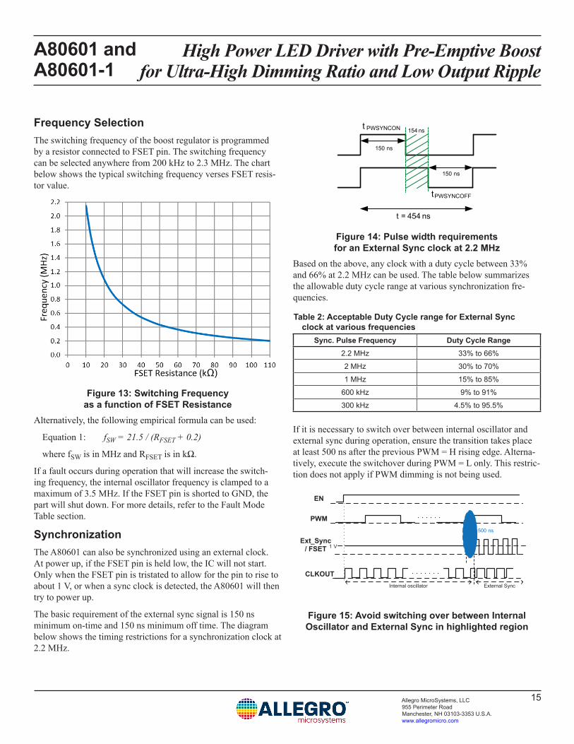
Frequency Selection The switching frequency of the boost regulator is programmed by a resistor connected to FSET pin. The switching frequency can be selected anywhere from 200 kHz to 2.3 MHz. The chart below shows the typical switching frequency verses FSET resis-tor value.
Figure 13: Switching Frequency as a function of FSET Resistance
Alternatively, the following empirical formula can be used:
Equation 1: fSW = 21.5 / (RFSET + 0.2)
where fSW is in MHz and RFSET is in kΩ.
If a fault occurs during operation that will increase the switch-ing frequency, the internal oscillator frequency is clamped to a maximum of 3.5 MHz. If the FSET pin is shorted to GND, the part will shut down. For more details, refer to the Fault Mode Table section.
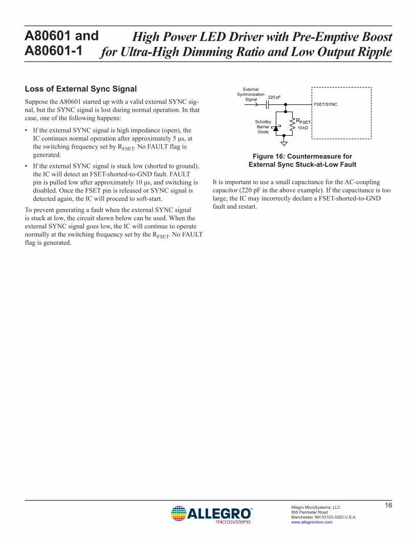
Synchronization The A80601 can also be synchronized using an external clock. At power up, if the FSET pin is held low, the IC will not start. Only when the FSET pin is tristated to allow for the pin to rise to about 1 V, or when a sync clock is detected, the A80601 will then try to power up.
The basic requirement of the external sync signal is 150 ns minimum on-time and 150 ns minimum off time. The diagram below shows the timing restrictions for a synchronization clock at 2.2 MHz.
150 ns
150 ns
t = 454 ns
154 nst PWSYNCON
tPWSYNCOFF
Figure 14: Pulse width requirements for an External Sync clock at 2.2 MHz
Based on the above, any clock with a duty cycle between 33% and 66% at 2.2 MHz can be used. The table below summarizes the allowable duty cycle range at various synchronization fre-quencies.
Table 2: Acceptable Duty Cycle range for External Sync clock at various frequencies
Sync. Pulse Frequency Duty Cycle Range2.2 MHz 33% to 66%
2 MHz 30% to 70%
1 MHz 15% to 85%
600 kHz 9% to 91%
300 kHz 4.5% to 95.5%
If it is necessary to switch over between internal oscillator and external sync during operation, ensure the transition takes place at least 500 ns after the previous PWM = H rising edge. Alterna-tively, execute the switchover during PWM = L only. This restric-tion does not apply if PWM dimming is not being used.
PWM
Ext_Sync/ FSET
CLKOUT
1 V
Internal oscillator External Sync
EN
500 ns
Figure 15: Avoid switching over between Internal Oscillator and External Sync in highlighted region
High Power LED Driver with Pre-Emptive Boost for Ultra-High Dimming Ratio and Low Output Ripple
A80601 and A80601-1
16Allegro MicroSystems, LLC 955 Perimeter Road Manchester, NH 03103-3353 U.S.A.www.allegromicro.com
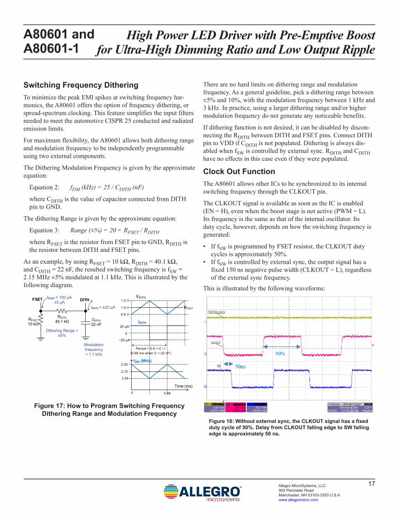
Loss of External Sync SignalSuppose the A80601 started up with a valid external SYNC sig-nal, but the SYNC signal is lost during normal operation. In that case, one of the following happens:
• If the external SYNC signal is high impedance (open), the IC continues normal operation after approximately 5 μs, at the switching frequency set by RFSET. No FAULT flag is generated.
• If the external SYNC signal is stuck low (shorted to ground), the IC will detect an FSET-shorted-to-GND fault. FAULT pin is pulled low after approximately 10 μs, and switching is disabled. Once the FSET pin is released or SYNC signal is detected again, the IC will proceed to soft-start.
To prevent generating a fault when the external SYNC signal is stuck at low, the circuit shown below can be used. When the external SYNC signal goes low, the IC will continue to operate normally at the switching frequency set by the RFSET. No FAULT flag is generated.
FSET/SYNC
External Sychronization
Signal
RFSET 10 kΩ
SchottkyBarrierDiode
220 pF
Figure 16: Countermeasure for External Sync Stuck-at-Low Fault
It is important to use a small capacitance for the AC-coupling capacitor (220 pF in the above example). If the capacitance is too large, the IC may incorrectly declare a FSET-shorted-to-GND fault and restart.
High Power LED Driver with Pre-Emptive Boost for Ultra-High Dimming Ratio and Low Output Ripple
A80601 and A80601-1
17Allegro MicroSystems, LLC 955 Perimeter Road Manchester, NH 03103-3353 U.S.A.www.allegromicro.com
Switching Frequency DitheringTo minimize the peak EMI spikes at switching frequency har-monics, the A80601 offers the option of frequency dithering, or spread-spectrum clocking. This feature simplifies the input filters needed to meet the automotive CISPR 25 conducted and radiated emission limits.
For maximum flexibility, the A80601 allows both dithering range and modulation frequency to be independently programmable using two external components.
The Dithering Modulation Frequency is given by the approximate equation:
Equation 2: fDM (kHz) = 25 / CDITH (nF)
where CDITH is the value of capacitor connected from DITH pin to GND.
The dithering Range is given by the approximate equation:
Equation 3: Range (±%) = 20 × RFSET / RDITH
where RFSET is the resistor from FSET pin to GND, RDITH is the resistor between DITH and FSET pins.
As an example, by using RFSET = 10 kΩ, RDITH = 40.1 kΩ, and CDITH = 22 nF, the resulted switching frequency is fSW = 2.15 MHz ±5% modulated at 1.1 kHz. This is illustrated by the following diagram.
FSET DITH
RDITH 40.1 kΩ CDITH
22 nFRFSET10 kΩ
iDITH = ±20 µA
iFSET = 100 µA ±5 µA
0.8 V
1.2 V
–20 µA
20 µAiDITH
VDITH
Per iod = 0.8 × C / i (0.88 ms when C = 22 nF)
Modulation frequency = 1.1 kHz
VFSET1.0 V
Dithering Range = ±5% 0
2.05
2.25
2.15
fSW (MHz)
Time (ms)0.880
Figure 17: How to Program Switching Frequency Dithering Range and Modulation Frequency
There are no hard limits on dithering range and modulation frequency. As a general guideline, pick a dithering range between ±5% and 10%, with the modulation frequency between 1 kHz and 3 kHz. In practice, using a larger dithering range and/or higher modulation frequency do not generate any noticeable benefits.
If dithering function is not desired, it can be disabled by discon-necting the RDITH between DITH and FSET pins. Connect DITH pin to VDD if CDITH is not populated. Dithering is always dis-abled when fSW is controlled by external sync. RDITH and CDITH have no effects in this case even if they were populated.
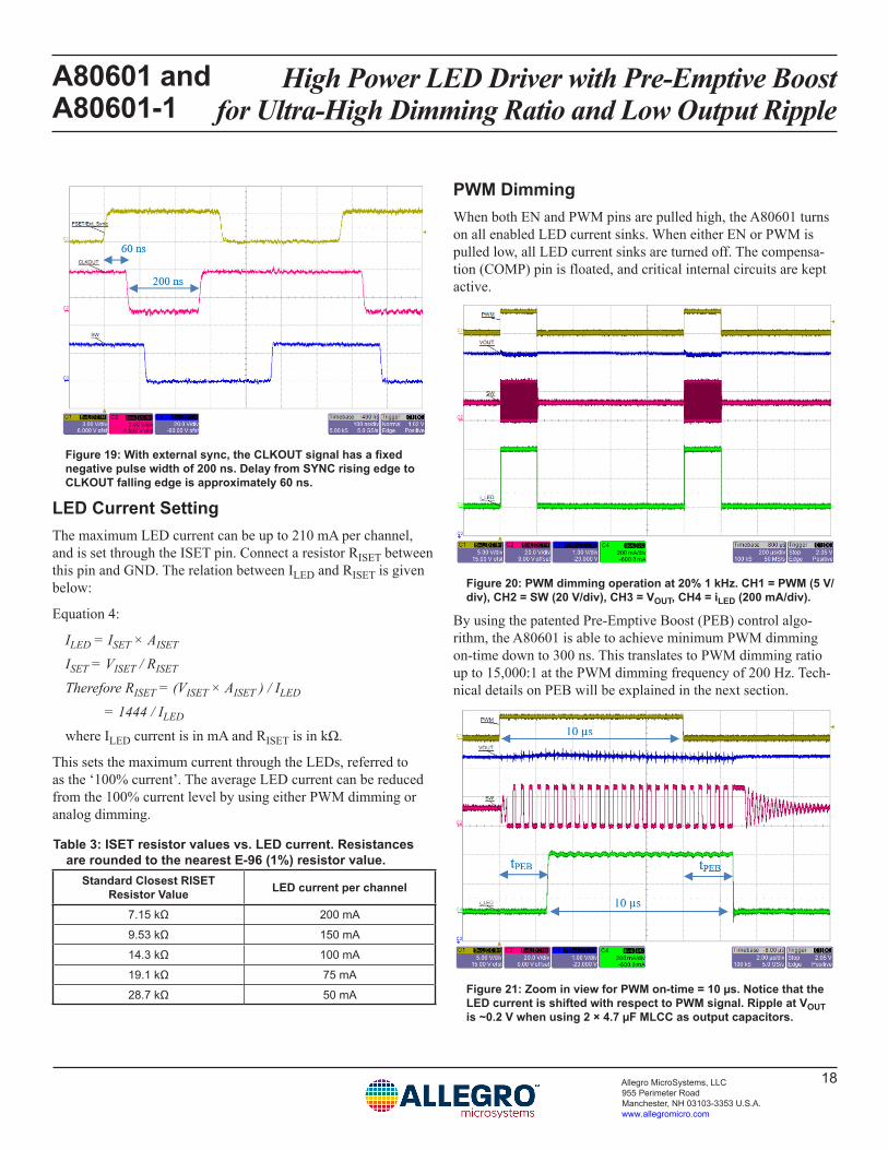
Clock Out FunctionThe A80601 allows other ICs to be synchronized to its internal switching frequency through the CLKOUT pin.
The CLKOUT signal is available as soon as the IC is enabled (EN = H), even when the boost stage is not active (PWM = L). Its frequency is the same as that of the internal oscillator. Its duty cycle, however, depends on how the switching frequency is generated:
• If fSW is programmed by FSET resistor, the CLKOUT duty cycles is approximately 50%.
• If fSW is controlled by external sync, the output signal has a fixed 150 ns negative pulse width (CLKOUT = L), regardless of the external sync frequency.
This is illustrated by the following waveforms:
Figure 18: Without external sync, the CLKOUT signal has a fixed duty cycle of 50%. Delay from CLKOUT falling edge to SW falling edge is approximately 50 ns.
High Power LED Driver with Pre-Emptive Boost for Ultra-High Dimming Ratio and Low Output Ripple
A80601 and A80601-1
18Allegro MicroSystems, LLC 955 Perimeter Road Manchester, NH 03103-3353 U.S.A.www.allegromicro.com
Figure 19: With external sync, the CLKOUT signal has a fixed negative pulse width of 200 ns. Delay from SYNC rising edge to CLKOUT falling edge is approximately 60 ns.
LED Current SettingThe maximum LED current can be up to 210 mA per channel, and is set through the ISET pin. Connect a resistor RISET between this pin and GND. The relation between ILED and RISET is given below:
Equation 4:
ILED = ISET × AISET
ISET = VISET / RISET
Therefore RISET = (VISET × AISET ) / ILED
= 1444 / ILED
where ILED current is in mA and RISET is in kΩ.
This sets the maximum current through the LEDs, referred to as the ‘100% current’. The average LED current can be reduced from the 100% current level by using either PWM dimming or analog dimming.
Table 3: ISET resistor values vs. LED current. Resistances are rounded to the nearest E-96 (1%) resistor value.
Standard Closest RISET Resistor Value LED current per channel
7.15 kΩ 200 mA
9.53 kΩ 150 mA
14.3 kΩ 100 mA
19.1 kΩ 75 mA
28.7 kΩ 50 mA
PWM DimmingWhen both EN and PWM pins are pulled high, the A80601 turns on all enabled LED current sinks. When either EN or PWM is pulled low, all LED current sinks are turned off. The compensa-tion (COMP) pin is floated, and critical internal circuits are kept active.
Figure 20: PWM dimming operation at 20% 1 kHz. CH1 = PWM (5 V/div), CH2 = SW (20 V/div), CH3 = VOUT, CH4 = iLED (200 mA/div).
By using the patented Pre-Emptive Boost (PEB) control algo-rithm, the A80601 is able to achieve minimum PWM dimming on-time down to 300 ns. This translates to PWM dimming ratio up to 15,000:1 at the PWM dimming frequency of 200 Hz. Tech-nical details on PEB will be explained in the next section.
Figure 21: Zoom in view for PWM on-time = 10 µs. Notice that the LED current is shifted with respect to PWM signal. Ripple at VOUT is ~0.2 V when using 2 × 4.7 µF MLCC as output capacitors.
High Power LED Driver with Pre-Emptive Boost for Ultra-High Dimming Ratio and Low Output Ripple
A80601 and A80601-1
19Allegro MicroSystems, LLC 955 Perimeter Road Manchester, NH 03103-3353 U.S.A.www.allegromicro.com
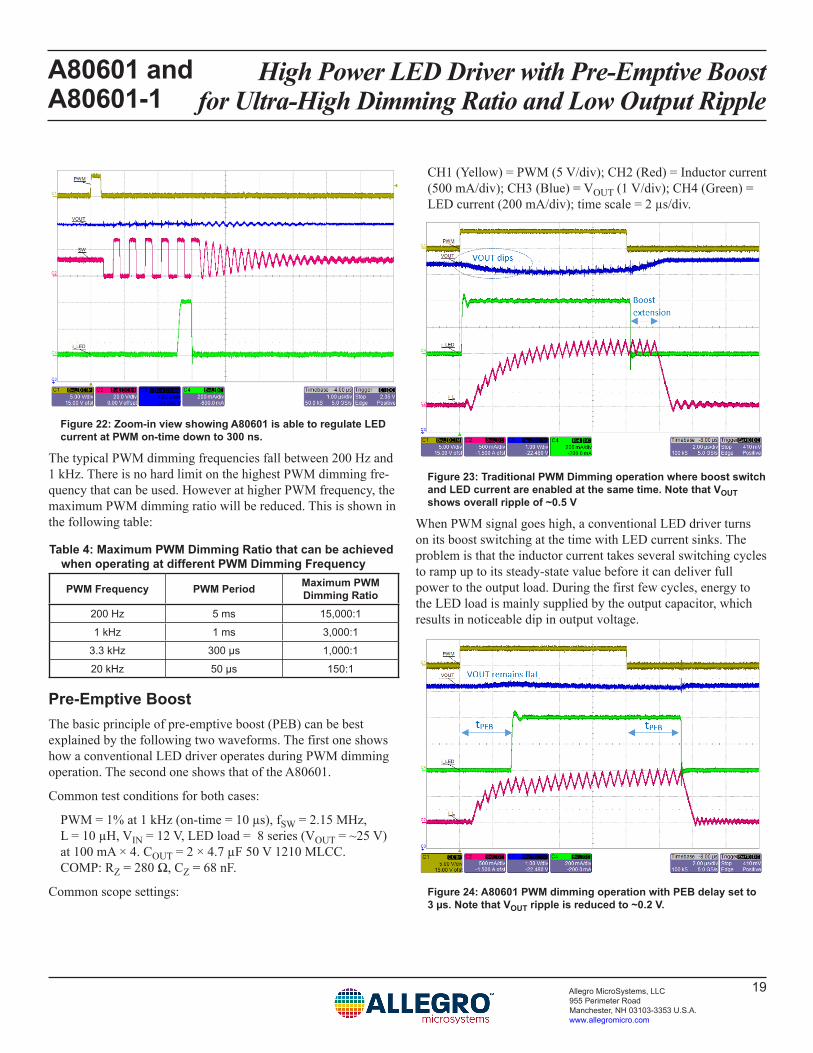
Figure 22: Zoom-in view showing A80601 is able to regulate LED current at PWM on-time down to 300 ns.
The typical PWM dimming frequencies fall between 200 Hz and 1 kHz. There is no hard limit on the highest PWM dimming fre-quency that can be used. However at higher PWM frequency, the maximum PWM dimming ratio will be reduced. This is shown in the following table:
Table 4: Maximum PWM Dimming Ratio that can be achieved when operating at different PWM Dimming Frequency
PWM Frequency PWM Period Maximum PWM Dimming Ratio
200 Hz 5 ms 15,000:1
1 kHz 1 ms 3,000:1
3.3 kHz 300 µs 1,000:1
20 kHz 50 µs 150:1
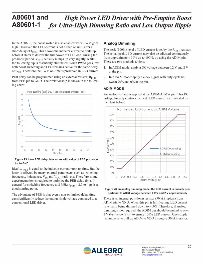
Pre-Emptive BoostThe basic principle of pre-emptive boost (PEB) can be best explained by the following two waveforms. The first one shows how a conventional LED driver operates during PWM dimming operation. The second one shows that of the A80601.
Common test conditions for both cases:
PWM = 1% at 1 kHz (on-time = 10 µs), fSW = 2.15 MHz, L = 10 µH, VIN = 12 V, LED load = 8 series (VOUT = ~25 V) at 100 mA × 4. COUT = 2 × 4.7 µF 50 V 1210 MLCC. COMP: RZ = 280 Ω, CZ = 68 nF.
Common scope settings:
CH1 (Yellow) = PWM (5 V/div); CH2 (Red) = Inductor current (500 mA/div); CH3 (Blue) = VOUT (1 V/div); CH4 (Green) = LED current (200 mA/div); time scale = 2 µs/div.
Figure 23: Traditional PWM Dimming operation where boost switch and LED current are enabled at the same time. Note that VOUT shows overall ripple of ~0.5 V
When PWM signal goes high, a conventional LED driver turns on its boost switching at the time with LED current sinks. The problem is that the inductor current takes several switching cycles to ramp up to its steady-state value before it can deliver full power to the output load. During the first few cycles, energy to the LED load is mainly supplied by the output capacitor, which results in noticeable dip in output voltage.
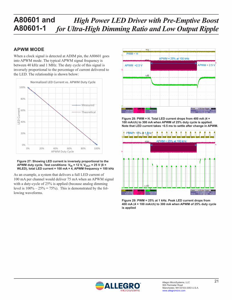
Figure 24: A80601 PWM dimming operation with PEB delay set to 3 µs. Note that VOUT ripple is reduced to ~0.2 V.
High Power LED Driver with Pre-Emptive Boost for Ultra-High Dimming Ratio and Low Output Ripple
A80601 and A80601-1
20Allegro MicroSystems, LLC 955 Perimeter Road Manchester, NH 03103-3353 U.S.A.www.allegromicro.com
In the A80601, the boost switch is also enabled when PWM goes high. However, the LED current is not turned on until after a short delay of tPEB. This allows the inductor current to build up before it starts to deliver the full power to LED load. During the pre-boost period, VOUT actually bumps up very slightly, while the following dip is essentially eliminated. When PWM goes low, both boost switching and LED remains active for the same delay of tPEB. Therefore the PWM on-time is preserved in LED current.
PEB delay can be programmed using an external resistor, RPEB, from PEB pin to GND. Their relationship is shown in the follow-ing chart:
0
1
2
3
4
5
6
7
8
9
10
6 8 10 12 14 16 18 20 22 24
t PEB
(µs)
RPEB (kΩ)
PEB Delay (µs) vs. PEB Resistor value (kΩ)
Figure 25: How PEB delay time varies with value of PEB pin resis-tor to GND.
Ideally, tPEB is equal to the inductor current ramp up time. But the latter is affected by many external parameters, such as switching frequency, inductance, VIN and VOUT ratio, etc. Therefore, some experimentation is required to optimize the PEB delay time. In general for switching frequency at 2 MHz, tPEB = 2.5 to 4 µs is a good starting point.
The advantage of PEB is that even a non-optimized delay time can significantly reduce the output ripple voltage compared to a conventional LED driver.
Analog DimmingThe peak (100%) level of LED current is set by the RISET resistor. The actual peak LED current may also be adjusted continuously from approximately 10% up to 100%, by using the ADIM pin. There are two methods to do so:
1. In ADIM mode: apply a DC voltage between 0.2 V and 2 V at the pin.
2. In APWM mode: apply a clock signal with duty cycle be-tween 90% and 0% at the pin.
ADIM MODEAn analog voltage is applied at the ADIM/APMW pin. This DC voltage linearly controls the peak LED current, as illustrated by the chart below:
0%
10%
20%
30%
40%
50%
60%
70%
80%
90%
100%
0 0.2 0.4 0.6 0.8 1 1.2 1.4 1.6 1.8 2 2.2
LED
Curr
ent
ADIM Voltage (V)
Normalized LED Current vs. ADIM Voltage
ADIM Decreasing
ADIM Increasing
Figure 26: In analog dimming mode, the LED current is linearly pro-portional to ADIM voltage between 0.2 V and 2 V approximately
There is an internal pull-down resistor (50 kΩ typical) from ADIM pin to GND. When this pin is left floating, LED current is actually being dimmed down to ~10%. Therefore, if analog dimming is not required, the ADIM pin should be pulled to over 2 V (but below VDD) to ensure 100% LED current. One simple technique is to pull up ADIM to VDD through a 30 kΩ resistor.
High Power LED Driver with Pre-Emptive Boost for Ultra-High Dimming Ratio and Low Output Ripple
A80601 and A80601-1
21Allegro MicroSystems, LLC 955 Perimeter Road Manchester, NH 03103-3353 U.S.A.www.allegromicro.com
APWM MODEWhen a clock signal is detected at ADIM pin, the A80601 goes into APWM mode. The typical APWM signal frequency is between 40 kHz and 1 MHz. The duty cycle of this signal is inversely proportional to the percentage of current delivered to the LED. The relationship is shown below:
0%
20%
40%
60%
80%
100%
0% 20% 40% 60% 80% 100%
LED
Curr
ent
APWM Duty Cycle
Normalized LED Current vs. APWM Duty Cycle
Measured
Theorecal
Figure 27: Showing LED current is inversely proportional to the APWM duty cycle. Test conditions: VIN = 12 V, VOUT = 25 V (8 × WLED), total LED current = 100 mA × 4, APWM frequency = 100 kHz
As an example, a system that delivers a full LED current of 100 mA per channel would deliver 75 mA when an APWM signal with a duty-cycle of 25% is applied (because analog dimming level is 100% – 25% = 75%). This is demonstrated by the fol-lowing waveforms.
Figure 28: PWM = H. Total LED current drops from 400 mA (4 × 100 mA/ch) to 300 mA when APWM of 25% duty cycle is applied. Note that LED current takes ~0.5 ms to settle after change in APWM.
Figure 29: PWM = 25% at 1 kHz. Peak LED current drops from 400 mA (4 × 100 mA/ch) to 300 mA when APWM of 25% duty cycle is applied
High Power LED Driver with Pre-Emptive Boost for Ultra-High Dimming Ratio and Low Output Ripple
A80601 and A80601-1
22Allegro MicroSystems, LLC 955 Perimeter Road Manchester, NH 03103-3353 U.S.A.www.allegromicro.com
One popular application of analog dimming is for LED brightness calibration, commonly known as ‘LED Binning’. LEDs from the same manufacturer and series are often grouped into differ-ent ‘bins’ according to their light efficacy (lumens per watt). It is therefore necessary to calibrate the ‘100% current’ for each LED bin, in order to achieve uniform luminosity.
To use ADIM pin as a trim function, the user should first set the 100% current based on efficacy of LED from the lowest bin. When using LED with higher efficacy, the required current is then trimmed down to the appropriate level using APWM duty cycle.
As an example, assume that:
• LED from lowest bin has an efficacy of 80 lm/W• LED highest bin has an efficacy of 120 lm/WSuppose the maximum LED current was set at 100 mA based on LEDs from lowest bin. When using LEDs from highest bin, the current should then be reduces to 67% (80/120). This can be achieved by sending APWM clock with 33% duty cycle.
Extending LED Dimming RatioThe dynamic range of LED brightness can be further extended, by using a combination of PWM duty cycle, APWM duty cycle, and analog dimming method.
For example, the following approach can be used to achieve a 100,000:1 dimming ratio at 200 Hz:
• Vary PWM duty cycle from 100% down to 0.01% to give 10,000:1 dimming. This requires PWM dimming on-time be reduced down to 0.5 µs.
• With PWM dimming on-time fixed at 0.5µs, vary APWM duty from 0% to 90% to reduce peak LED current from 100% down to 10%. This gives a net effect of 100,000:1 dimming.
0.001
0.01
0.1
1
10
100
0.001 0.01 0.1 1 10 100N
orm
alize
d LE
D Cu
rren
t (%
)PWM Dimming Duty Cycle (%)
Average LED Current vs. PWM Dimming Duty Cycle
PWM Dimming
APWM + PWM
Ideal
Figure 30: How to achieve 100,000:1 dimming ratio by using both PWM and APWM. Test conditions: VIN = 12 V, VOUT = 25 V (8 × WLED), total LED current = 400 mA, PWM frequency = 200 Hz, APWM frequency = 100 kHz.
Note that the A80601 is capable of providing analog dimming range greater than 10:1. By applying APWM with 96% duty cycle, for example, an analog dimming range of 25:1 can be achieved. However, this requires the external APWM signal source to have very fine pulse-width resolution. At 200 kHz APWM frequency, a resolution of 50 ns is required to adjust its duty cycle by 1%.
High Power LED Driver with Pre-Emptive Boost for Ultra-High Dimming Ratio and Low Output Ripple
A80601 and A80601-1
23Allegro MicroSystems, LLC 955 Perimeter Road Manchester, NH 03103-3353 U.S.A.www.allegromicro.com
Analog Dimming with External VoltageBesides using ADIM pin, the LED current can also be reduced by using an external voltage source applied through a resistor to the ISET pin. The dynamic range of this type of dimming is dependent on the ISET pin current. The recommended iSET range is from 20 µA to 144 µA for the A80601. Note that the IC will continue to work at iSET below 20 µA, but the relative error in LED current becomes larger at lower dimming level.
Below is a typical application circuit using a DAC (digital-analog converter) to control the LED current. The ISET current (which directly controls the LED current) is normally set as VISET/RISET. The DAC voltage can be higher or lower than VISET, thus adjust-ing the LED current to a lower or higher value.
RISET
A80601R2
ISET
GND
VDAC
Figure 31: Adjusting LED current with an external voltage source
Equation 5:
−
−=2R
VVDACRV
iISETISET
ISET
SETI
where VISET is the ISET pin voltage (typically 1.0 V), and VDAC is the DAC output voltage.
When VDAC is higher than 1.00 V, the LED current is reduced. When VDAC is lower than 1.00 V, the LED current is increased.
Some common applications for the above scheme include:
• LED binning• Thermal fold-back using external NTC (negative temperature
coefficient) thermistor
In the following application example, the thermistor used is NTC-S0805E3684JXT (680 kΩ @ 25°C). R1 = 336 kΩ, R2 = 20 kΩ, and R3 = 8.45 kΩ. The LED current per channel is reduced from 97 mA at 25°C to 34 mA at 125°C.
VDD (4.25 V)
ISET (1.0 V)
NTC
R1
R2
R3
A80601
GND
Figure 32: Thermal foldback of LED current using NTC thermistor
Figure 33: LED current varies with temperature when using thermistor NTCS0805E3684JXT
for thermal foldback
High Power LED Driver with Pre-Emptive Boost for Ultra-High Dimming Ratio and Low Output Ripple
A80601 and A80601-1
24Allegro MicroSystems, LLC 955 Perimeter Road Manchester, NH 03103-3353 U.S.A.www.allegromicro.com
VDD The VDD pin provides regulated bias supply for internal circuits. Connect a CVDD capacitor with a value of 1 μF or greater to this pin. The internal LDO can deliver up to 2 mA of current exter-nally with a typical VDD voltage of about 4.25 V. This allows it to serve as the pull up voltage for FAULT pin.
VDRV The VDRV pin provides a regulated gate driver supply for external boost power MOSFET. Connect a CVDRV capacitor with a typical value of 2.2 μF to this pin. The gate driver can deliver up to 2 A of peak sink and source current, with a typical VDRV voltage of 6.5 V. However, its average output current is limited to approximately 36 mA. Note that average gate driver current is:
Equation 6: iVDRV = fSW × QG
where fSW is the switching frequency and QG is the total gate charge of the power MOSFET for VGS = 0 to 6.5 V.
At higher switching frequency, it is important to select a power MOSFET with low QG to limit the average gate driver current. Refer to the appendix section for details on MOSFET selection.
ShutdownIf EN pin is pulled low for longer than tEN(OFF) (~16 ms), the A80601 enters shutdown (sleep mode). The next time EN pin goes high, all internal fault registers are cleared. The IC needs to go through a complete soft start process after PWM goes high.
Figure 34: After EN = L for ~16 ms, the IC completely shuts down so VDD (Blue) decays.
There is an alternative way to reset the internal fault status reg-isters. By keeping EN = H and PWM = L for longer than 16 ms, the A80601 clears all internal fault registers but does not go into sleep mode. The next time PWM pin goes high, the IC will still go through soft start process. The difference is that VDD voltage and CLKOUT signal are always available as long as EN = H.
Figure 35: As long as EN = H, the IC does not shut down VDD and CLKOUT. But internal latched faults are cleared by PWM = L for ~16 ms.
High Power LED Driver with Pre-Emptive Boost for Ultra-High Dimming Ratio and Low Output Ripple
A80601 and A80601-1
25Allegro MicroSystems, LLC 955 Perimeter Road Manchester, NH 03103-3353 U.S.A.www.allegromicro.com
FAULT DETECTION AND PROTECTION
FAULT StatusThe FAULT pin is an open-drain output that will be pulled low when a fault occurs. A pull-up resistor (typically around 10 kΩ) is required between this pin and desired logic level voltage (typi-cally 3.3 to 5 V). Multiple devices with open-drain FAULT pins can be connected in parallel to form a wired-AND configuration. This way, when any device reports a fault, the system FAULT signal is pulled low.
The A80601-1 (One-Out-All-Out option) has a bidirectional FAULT pin. This means the same pin also serves as an input to monitor the status of system FAULT signal. When the FAULT pin is pulled low externally for >8 fSW cycles by another device, the A80601-1 disables its own boost switch and all LED current sinks in response. This feature is required in Master/Slave con-figuration, for example.
The following two simplified flow charts demonstrate the differ-ence between A80601 (unidirectional FAULT pin) and A80601-1 (bidirectional FAULT pin).
Any Fault detected?
IC Off
Power up(VCC, BG ready; GATE pulled L; Fault checking)
FAULT State(FAULT pulled L )
Yes
No
IC Ready(CLKOUT active,FAULT pulled L )
EN=H & VIN>UVLO
Soft Start(enable boost SW and
LED current sinks)
EN=H & PWM=L
EN=L
EN=L
Any Fault detected? Yes
No
LED=onClear 16ms timer
EN && PWM =L
LED=offStart 16ms timer Timer expired
EN && PWM =H
PWM Dimming
EN=H & PWM=H
LED Pin Check(In Use, Disabled, or
Shorted to GND)
Pin shorted to GND fault FAULT =L
Time-out without faults FAULT released
Figure 36: Simplified A80601 Startup Flowchart
High Power LED Driver with Pre-Emptive Boost for Ultra-High Dimming Ratio and Low Output Ripple
A80601 and A80601-1
26Allegro MicroSystems, LLC 955 Perimeter Road Manchester, NH 03103-3353 U.S.A.www.allegromicro.com
Any Internal Fault detected?
IC Off
Power up(VCC, BG ready; GATE pulled L; Fault checking)
FAULT State(FAULT pulled L)
Yes
No
IC Ready(CLKOUT active,FAULT pulled L)
EN=H & VIN>UVLO
Soft Start(enable boost SW and
LED current sinks)
EN=H & PWM=L
EN=L
EN=L
Any Internal Fault detected? Yes
No
LED=onClear 16ms timer
EN && PWM =L
LED=offStart 16ms timer Timer expired
EN && PWM =H
PWM Dimming
Any ExternalFault detected?Yes
(FAULT pulled L externally) No
(FAULT=H)
Any ExternalFault detected?
No
EN=H & PWM=H
LED Pin Check(In Use, Disabled, or
Shorted to GND)
Pin shorted to GND fault FAULT=L
Time-out without faults FAULT released
Yes(FAULT pulled L
externally)
Figure 37: Simplified startup flow chart for A80601-1, showing responses to both Internal and External FAULT signals
High Power LED Driver with Pre-Emptive Boost for Ultra-High Dimming Ratio and Low Output Ripple
A80601 and A80601-1
27Allegro MicroSystems, LLC 955 Perimeter Road Manchester, NH 03103-3353 U.S.A.www.allegromicro.com
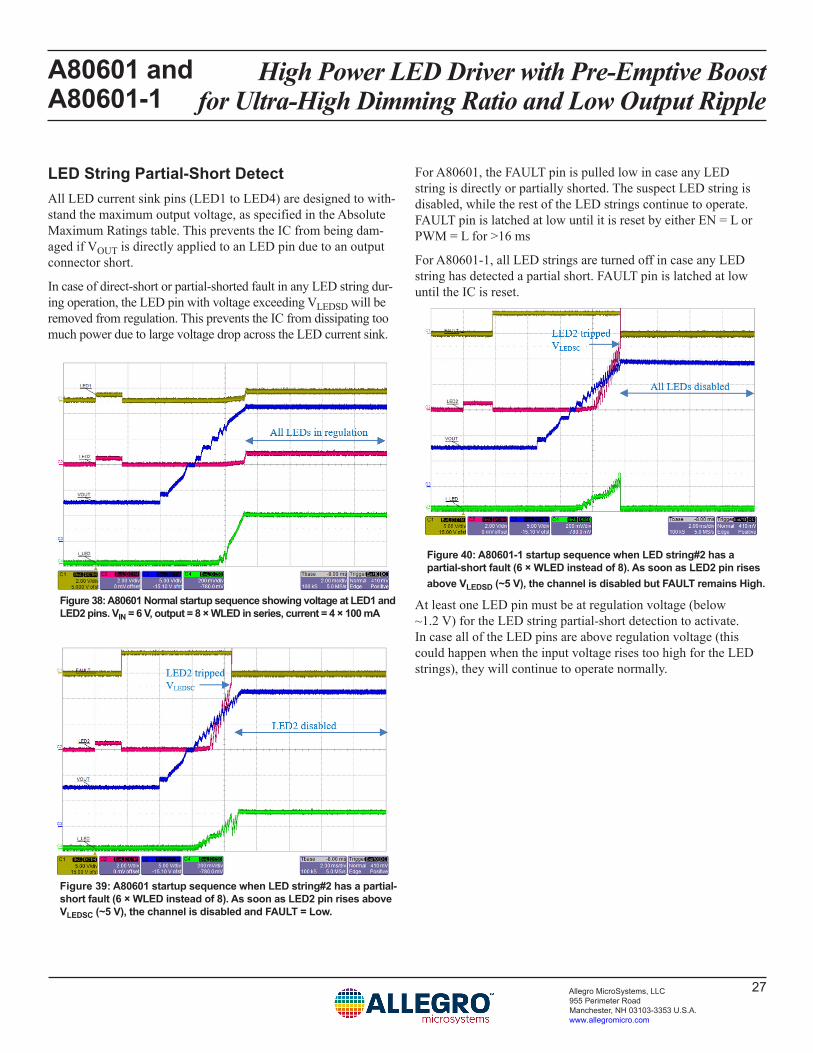
LED String Partial-Short Detect All LED current sink pins (LED1 to LED4) are designed to with-stand the maximum output voltage, as specified in the Absolute Maximum Ratings table. This prevents the IC from being dam-aged if VOUT is directly applied to an LED pin due to an output connector short.
In case of direct-short or partial-shorted fault in any LED string dur-ing operation, the LED pin with voltage exceeding VLEDSD will be removed from regulation. This prevents the IC from dissipating too much power due to large voltage drop across the LED current sink.
Figure 38: A80601 Normal startup sequence showing voltage at LED1 and LED2 pins. VIN = 6 V, output = 8 × WLED in series, current = 4 × 100 mA
Figure 39: A80601 startup sequence when LED string#2 has a partial-short fault (6 × WLED instead of 8). As soon as LED2 pin rises above VLEDSC (~5 V), the channel is disabled and FAULT = Low.
For A80601, the FAULT pin is pulled low in case any LED string is directly or partially shorted. The suspect LED string is disabled, while the rest of the LED strings continue to operate. FAULT pin is latched at low until it is reset by either EN = L or PWM = L for >16 ms
For A80601-1, all LED strings are turned off in case any LED string has detected a partial short. FAULT pin is latched at low until the IC is reset.
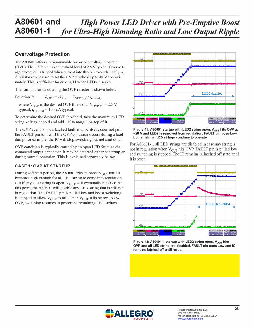
Figure 40: A80601-1 startup sequence when LED string#2 has a partial-short fault (6 × WLED instead of 8). As soon as LED2 pin rises above VLEDSD (~5 V), the channel is disabled but FAULT remains High.
At least one LED pin must be at regulation voltage (below ~1.2 V) for the LED string partial-short detection to activate. In case all of the LED pins are above regulation voltage (this could happen when the input voltage rises too high for the LED strings), they will continue to operate normally.
High Power LED Driver with Pre-Emptive Boost for Ultra-High Dimming Ratio and Low Output Ripple
A80601 and A80601-1
28Allegro MicroSystems, LLC 955 Perimeter Road Manchester, NH 03103-3353 U.S.A.www.allegromicro.com
Overvoltage ProtectionThe A80601 offers a programmable output overvoltage protection (OVP). The OVP pin has a threshold level of 2.5 V typical. Overvolt-age protection is tripped when current into this pin exceeds ~150 µA. A resistor can be used to set the OVP threshold up to 40 V approxi-mately. This is sufficient for driving 11 white LEDs in series.
The formula for calculating the OVP resistor is shown below:
Equation 7: ROVP = (VOVP – VOVP(th)) / iOVP(th)
where VOVP is the desired OVP threshold, VOVP(th) = 2.5 V typical, iOVP(th) = 150 µA typical.
To determine the desired OVP threshold, take the maximum LED string voltage at cold and add ~10% margin on top of it.
The OVP event is not a latched fault and, by itself, does not pull the FAULT pin to low. If the OVP condition occurs during a load dump, for example, the IC will stop switching but not shut down.
OVP condition is typically caused by an open LED fault, or dis-connected output connector. It may be detected either at startup or during normal operation. This is explained separately below.
CASE 1: OVP AT STARTUPDuring soft start period, the A80601 tries to boost VOUT until it becomes high enough for all LED string to come into regulation. But if any LED string is open, VOUT will eventually hit OVP. At this point, the A80601 will disable any LED string that is still not in regulation. The FAULT pin is pulled low and boost switching is stopped to allow VOUT to fall. Once VOUT falls below ~97% OVP, switching resumes to power the remaining LED strings.
Figure 41: A80601 startup with LED2 string open. VOUT hits OVP at ~28 V and LED2 is removed from regulation. FAULT pin goes Low but remaining LED strings continue to operate.
For A80601-1, all LED strings are disabled in case any string is not in regulation when VOUT hits OVP. FAULT pin is pulled low and switching is stopped. The IC remains in latched off state until it is reset.
Figure 42: A80601-1 startup with LED2 string open. VOUT hits OVP and all LED string are disabled. FAULT pin goes Low and IC remains latched off until reset.
High Power LED Driver with Pre-Emptive Boost for Ultra-High Dimming Ratio and Low Output Ripple
A80601 and A80601-1
29Allegro MicroSystems, LLC 955 Perimeter Road Manchester, NH 03103-3353 U.S.A.www.allegromicro.com
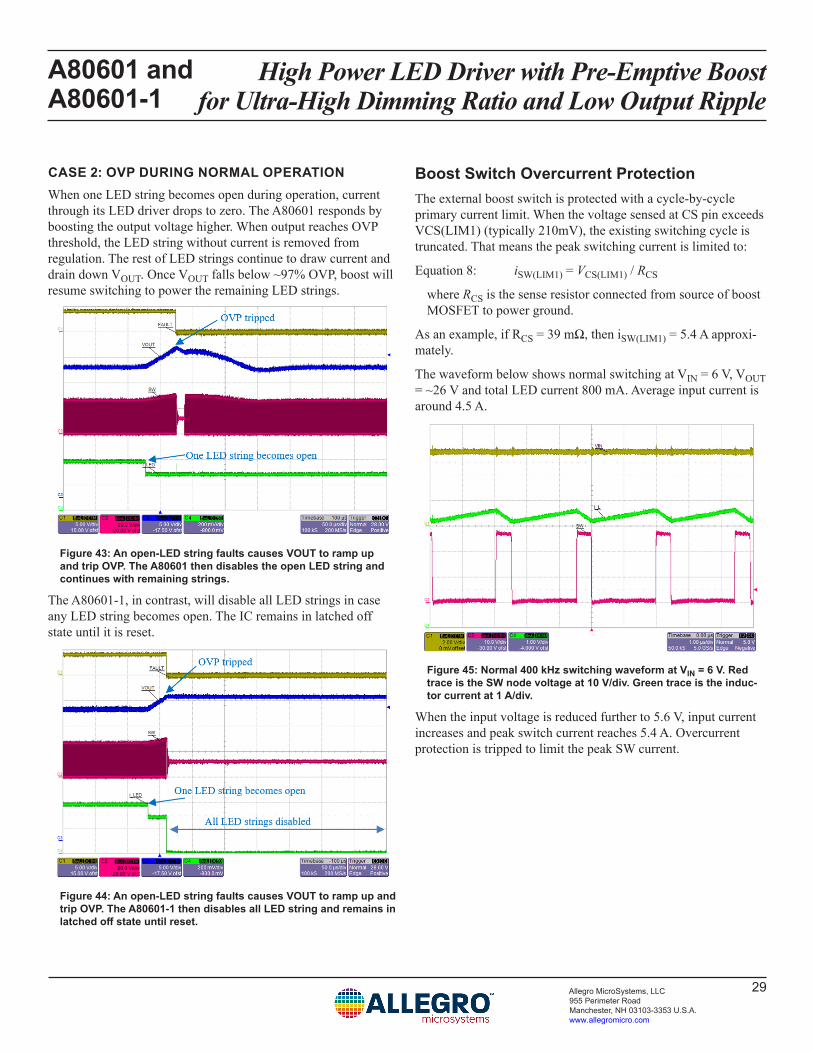
CASE 2: OVP DURING NORMAL OPERATIONWhen one LED string becomes open during operation, current through its LED driver drops to zero. The A80601 responds by boosting the output voltage higher. When output reaches OVP threshold, the LED string without current is removed from regulation. The rest of LED strings continue to draw current and drain down VOUT. Once VOUT falls below ~97% OVP, boost will resume switching to power the remaining LED strings.
Figure 43: An open-LED string faults causes VOUT to ramp up and trip OVP. The A80601 then disables the open LED string and continues with remaining strings.
The A80601-1, in contrast, will disable all LED strings in case any LED string becomes open. The IC remains in latched off state until it is reset.
Figure 44: An open-LED string faults causes VOUT to ramp up and trip OVP. The A80601-1 then disables all LED string and remains in latched off state until reset.
Boost Switch Overcurrent ProtectionThe external boost switch is protected with a cycle-by-cycle primary current limit. When the voltage sensed at CS pin exceeds VCS(LIM1) (typically 210mV), the existing switching cycle is truncated. That means the peak switching current is limited to:
Equation 8: iSW(LIM1) = VCS(LIM1) / RCS
where RCS is the sense resistor connected from source of boost MOSFET to power ground.
As an example, if RCS = 39 mΩ, then iSW(LIM1) = 5.4 A approxi-mately.
The waveform below shows normal switching at VIN = 6 V, VOUT = ~26 V and total LED current 800 mA. Average input current is around 4.5 A.
Figure 45: Normal 400 kHz switching waveform at VIN = 6 V. Red trace is the SW node voltage at 10 V/div. Green trace is the induc-tor current at 1 A/div.
When the input voltage is reduced further to 5.6 V, input current increases and peak switch current reaches 5.4 A. Overcurrent protection is tripped to limit the peak SW current.
High Power LED Driver with Pre-Emptive Boost for Ultra-High Dimming Ratio and Low Output Ripple
A80601 and A80601-1
30Allegro MicroSystems, LLC 955 Perimeter Road Manchester, NH 03103-3353 U.S.A.www.allegromicro.com
Figure 46: When peak current through the inductor reaches ~5.4 A, overcurrent protection kicks in to truncate the present switching cycle.
There is also a secondary current sense limit VCS(LIM2), set at about 40% higher than the cycle-by-cycle current limit. It is to protect the external MOSFET from destructive current spikes in case the boost inductor or boost diode is shorted. Once this limit is tripped, the A80601 will immediately shut down and latch off.
Input Overcurrent Protection and Disconnect Switch
A80601
Q1 (PMOS)
GATEVSENSE
VIN
RSENSERADJ
VIN
CG
To L1
VIN – VSENSE = RSC × iSENSE + RADJ × iADJ
iADJ
iSENSE
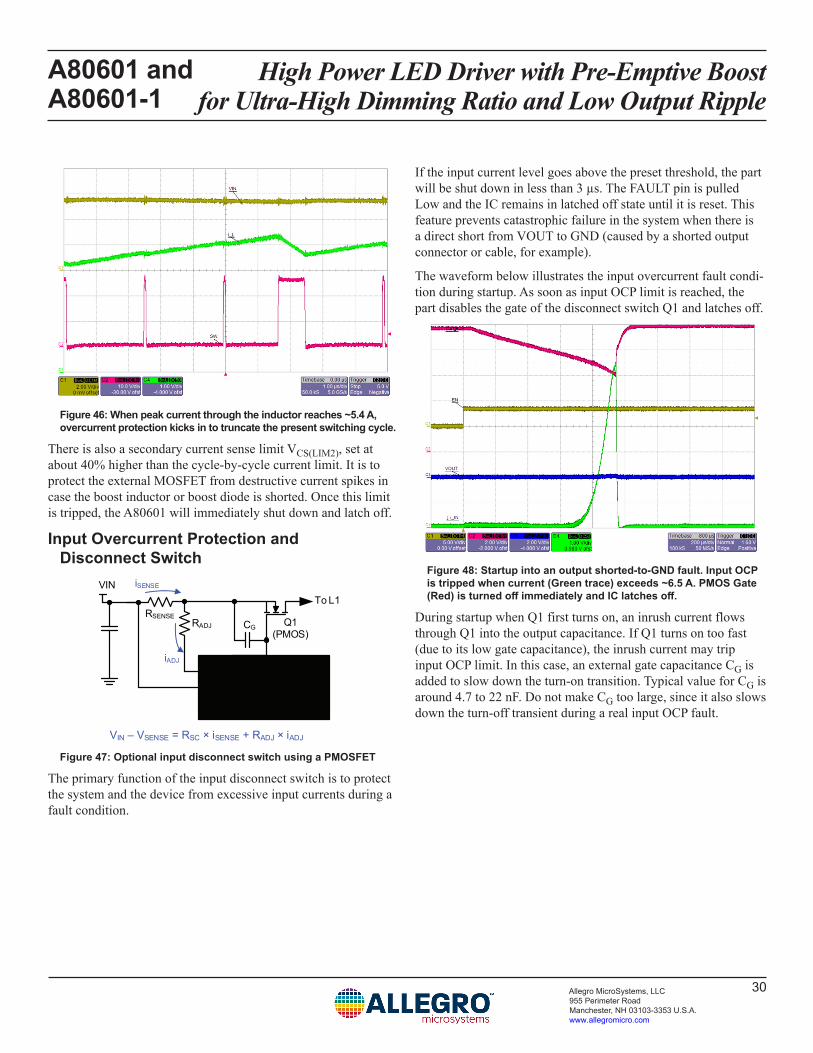
Figure 47: Optional input disconnect switch using a PMOSFET
The primary function of the input disconnect switch is to protect the system and the device from excessive input currents during a fault condition.
If the input current level goes above the preset threshold, the part will be shut down in less than 3 µs. The FAULT pin is pulled Low and the IC remains in latched off state until it is reset. This feature prevents catastrophic failure in the system when there is a direct short from VOUT to GND (caused by a shorted output connector or cable, for example).
The waveform below illustrates the input overcurrent fault condi-tion during startup. As soon as input OCP limit is reached, the part disables the gate of the disconnect switch Q1 and latches off.
Figure 48: Startup into an output shorted-to-GND fault. Input OCP is tripped when current (Green trace) exceeds ~6.5 A. PMOS Gate (Red) is turned off immediately and IC latches off.
During startup when Q1 first turns on, an inrush current flows through Q1 into the output capacitance. If Q1 turns on too fast (due to its low gate capacitance), the inrush current may trip input OCP limit. In this case, an external gate capacitance CG is added to slow down the turn-on transition. Typical value for CG is around 4.7 to 22 nF. Do not make CG too large, since it also slows down the turn-off transient during a real input OCP fault.

High Power LED Driver with Pre-Emptive Boost for Ultra-High Dimming Ratio and Low Output Ripple
A80601 and A80601-1
31Allegro MicroSystems, LLC 955 Perimeter Road Manchester, NH 03103-3353 U.S.A.www.allegromicro.com
Setting the Input Current Sense ResistorThe input disconnect switch threshold is typically 98 mV, mea-sured between VIN and VSENSE pins when RADJ is 0 Ω. This threshold can be trimmed slightly using the RADJ resistor.
To avoid false tripping, the input disconnect switch overcurrent limit should be set higher than the boost switch cycle-by-cycle cur-rent limit. For example, the boost switch OCP is set at 5.4 A, so the input disconnect switch OCP may be set 25% higher at 6.75 A. The input current sense resistor is then calculated as below.
When RADJ is not used:
VIN – VSENSE = RSENSE × iSENSE = 98 mV
The desired sense resistor is RSENSE = 98 mV / 6.75 A = 14.5 mΩ. But this is not a standard E-24 resistor value. Pick the closest lower value which is 13 mΩ.
When RADJ is used:
VIN – VSENSE = RSENSE × iSENSE + RADJ × iADJ
Therefore
RADJ = [(VIN – VSENSE) – (RSENSE × iSENSE)] / iADJ
= [98 mV – 88 mV] / 20 µA = 500 Ω
Pick the closest E-96 resistor value of 499 Ω.
Input UVLOWhen VIN rises above VUVLOrise threshold, the A80601 is enabled. The IC is disabled when VIN falls below VUVLOfall threshold for more than 50 μs. This small delay is used to avoid shutting down because of momentary glitches in the input power supply.
Fault Protection During Operation The A80601 constantly monitors the state of the system to deter-mine if any fault conditions occur during normal operation. The response to a triggered fault condition is summarized in the table below. It is important to note that there are several points at which the A80601 monitors for faults during operation. The locations are input current, switch current, output voltage, switch voltage, and LED pins. Some of the protection features might not be active dur-ing startup to prevent false triggering of fault conditions.
The possible fault conditions that the part can detect include:
• Open LED Pin or open LED string• Shorted or partially shorted LED string• LED pin shorted to GND• Open or shorted boost diode• Open or shorted boost inductor• VOUT short to GND• SW shorted to GND• ISET shorted to GND• FSET shorted to GND• Input disconnect switch drain shorted to GNDNote that some of these faults will not be protected if the input disconnect switch is not being used. An example of this is VOUT short to GND fault.
High Power LED Driver with Pre-Emptive Boost for Ultra-High Dimming Ratio and Low Output Ripple
A80601 and A80601-1
32Allegro MicroSystems, LLC 955 Perimeter Road Manchester, NH 03103-3353 U.S.A.www.allegromicro.com
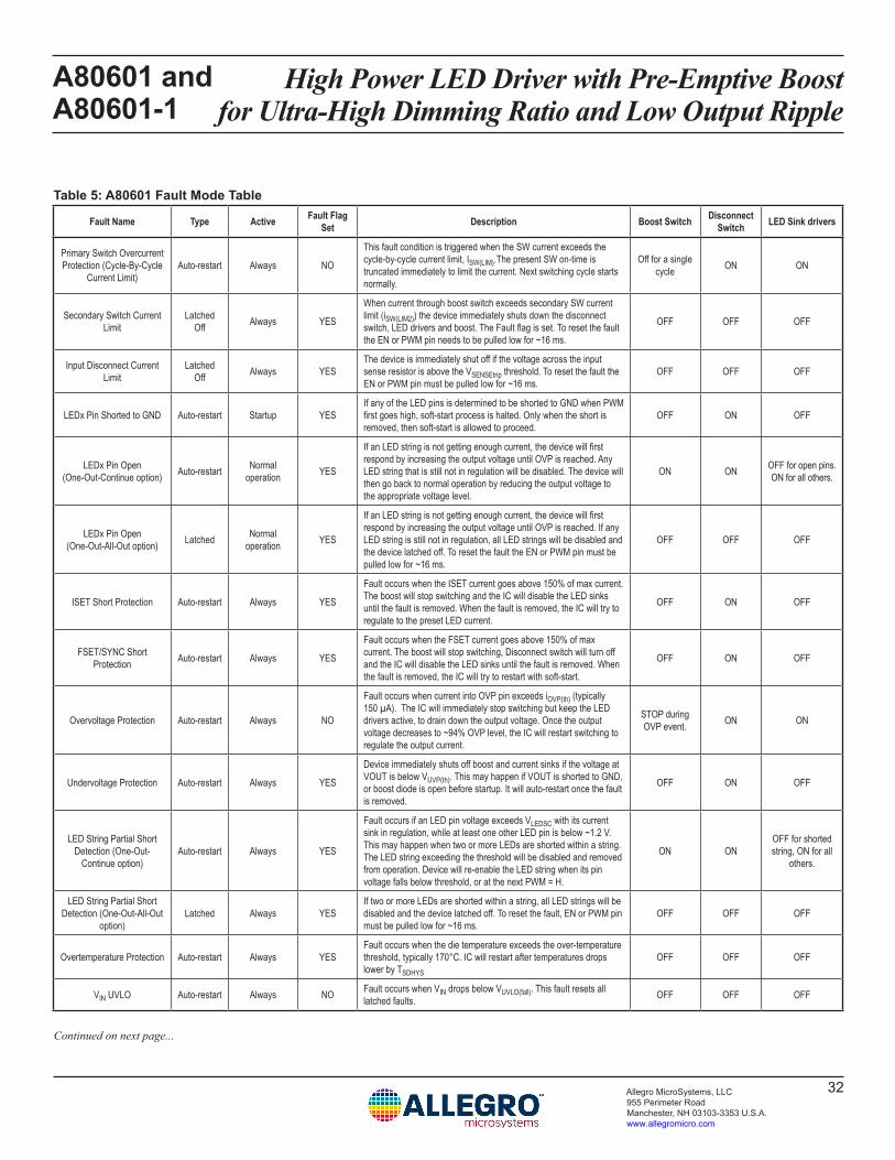
Table 5: A80601 Fault Mode Table
Fault Name Type Active Fault Flag Set Description Boost Switch Disconnect
Switch LED Sink drivers
Primary Switch Overcurrent Protection (Cycle-By-Cycle
Current Limit)Auto-restart Always NO
This fault condition is triggered when the SW current exceeds the cycle-by-cycle current limit, ISW(LIM).The present SW on-time is truncated immediately to limit the current. Next switching cycle starts normally.
Off for a single cycle ON ON
Secondary Switch Current Limit
Latched Off Always YES
When current through boost switch exceeds secondary SW current limit (iSW(LIM2)) the device immediately shuts down the disconnect switch, LED drivers and boost. The Fault flag is set. To reset the fault the EN or PWM pin needs to be pulled low for ~16 ms.
OFF OFF OFF
Input Disconnect Current Limit
Latched Off Always YES
The device is immediately shut off if the voltage across the input sense resistor is above the VSENSEtrip threshold. To reset the fault the EN or PWM pin must be pulled low for ~16 ms.
OFF OFF OFF
LEDx Pin Shorted to GND Auto-restart Startup YESIf any of the LED pins is determined to be shorted to GND when PWM first goes high, soft-start process is halted. Only when the short is removed, then soft-start is allowed to proceed.
OFF ON OFF
LEDx Pin Open (One-Out-Continue option) Auto-restart Normal
operation YES
If an LED string is not getting enough current, the device will first respond by increasing the output voltage until OVP is reached. Any LED string that is still not in regulation will be disabled. The device will then go back to normal operation by reducing the output voltage to the appropriate voltage level.
ON ON OFF for open pins.ON for all others.
LEDx Pin Open (One-Out-All-Out option) Latched Normal
operation YES
If an LED string is not getting enough current, the device will first respond by increasing the output voltage until OVP is reached. If any LED string is still not in regulation, all LED strings will be disabled and the device latched off. To reset the fault the EN or PWM pin must be pulled low for ~16 ms.
OFF OFF OFF
ISET Short Protection Auto-restart Always YES
Fault occurs when the ISET current goes above 150% of max current. The boost will stop switching and the IC will disable the LED sinks until the fault is removed. When the fault is removed, the IC will try to regulate to the preset LED current.
OFF ON OFF
FSET/SYNC Short Protection Auto-restart Always YES
Fault occurs when the FSET current goes above 150% of max current. The boost will stop switching, Disconnect switch will turn off and the IC will disable the LED sinks until the fault is removed. When the fault is removed, the IC will try to restart with soft-start.
OFF ON OFF
Overvoltage Protection Auto-restart Always NO
Fault occurs when current into OVP pin exceeds iOVP(th) (typically 150 µA). The IC will immediately stop switching but keep the LED drivers active, to drain down the output voltage. Once the output voltage decreases to ~94% OVP level, the IC will restart switching to regulate the output current.
STOP during OVP event. ON ON
Undervoltage Protection Auto-restart Always YES
Device immediately shuts off boost and current sinks if the voltage at VOUT is below VUVP(th). This may happen if VOUT is shorted to GND, or boost diode is open before startup. It will auto-restart once the fault is removed.
OFF ON OFF
LED String Partial Short Detection (One-Out-
Continue option)Auto-restart Always YES
Fault occurs if an LED pin voltage exceeds VLEDSC with its current sink in regulation, while at least one other LED pin is below ~1.2 V. This may happen when two or more LEDs are shorted within a string. The LED string exceeding the threshold will be disabled and removed from operation. Device will re-enable the LED string when its pin voltage falls below threshold, or at the next PWM = H.
ON ONOFF for shorted string, ON for all
others.
LED String Partial Short Detection (One-Out-All-Out
option)Latched Always YES
If two or more LEDs are shorted within a string, all LED strings will be disabled and the device latched off. To reset the fault, EN or PWM pin must be pulled low for ~16 ms.
OFF OFF OFF
Overtemperature Protection Auto-restart Always YESFault occurs when the die temperature exceeds the over-temperature threshold, typically 170°C. IC will restart after temperatures drops lower by TSDHYS
OFF OFF OFF
VIN UVLO Auto-restart Always NO Fault occurs when VIN drops below VUVLO(fall). This fault resets all latched faults. OFF OFF OFF
Continued on next page...
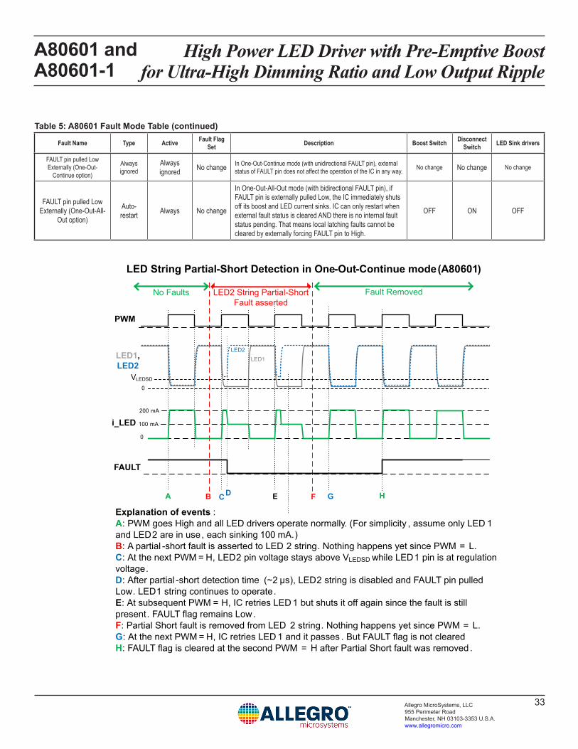
High Power LED Driver with Pre-Emptive Boost for Ultra-High Dimming Ratio and Low Output Ripple
A80601 and A80601-1
33Allegro MicroSystems, LLC 955 Perimeter Road Manchester, NH 03103-3353 U.S.A.www.allegromicro.com
Table 5: A80601 Fault Mode Table (continued)
Fault Name Type Active Fault Flag Set Description Boost Switch Disconnect
Switch LED Sink drivers
FAULT pin pulled Low Externally (One-Out-
Continue option)
Always ignored
Always ignored No change In One-Out-Continue mode (with unidirectional FAULT pin), external
status of FAULT pin does not affect the operation of the IC in any way. No change No change No change
FAULT pin pulled Low Externally (One-Out-All-
Out option)
Auto-restart Always No change
In One-Out-All-Out mode (with bidirectional FAULT pin), if FAULT pin is externally pulled Low, the IC immediately shuts off its boost and LED current sinks. IC can only restart when external fault status is cleared AND there is no internal fault status pending. That means local latching faults cannot be cleared by externally forcing FAULT pin to High.
OFF ON OFF
LED String Partial-Short Detection in One-Out-Continue mode (A80601)
FAULT
LED1,LED2
LED2 String Partial-Short Fault asserted
No Faults Fault Removed
0
A B C F G H
Explanation of events :A: PWM goes High and all LED drivers operate normally. (For simplicity , assume only LED 1 and LED2 are in use, each sinking 100 mA.)B: A partial -short fault is asserted to LED 2 string. Nothing happens yet since PWM = L.C: At the next PWM = H, LED2 pin voltage stays above VLEDSD while LED1 pin is at regulation voltage.D: After partial -short detection time (~2 µs), LED2 string is disabled and FAULT pin pulled Low. LED1 string continues to operate.E: At subsequent PWM = H, IC retries LED 1 but shuts it off again since the fault is still present. FAULT flag remains Low.F: Partial Short fault is removed from LED 2 string. Nothing happens yet since PWM = L.G: At the next PWM = H, IC retries LED 1 and it passes . But FAULT flag is not clearedH: FAULT flag is cleared at the second PWM = H after Partial Short fault was removed .
PWM
i_LED0
100 mA
200 mA
VLEDSD
D E
LED2LED1
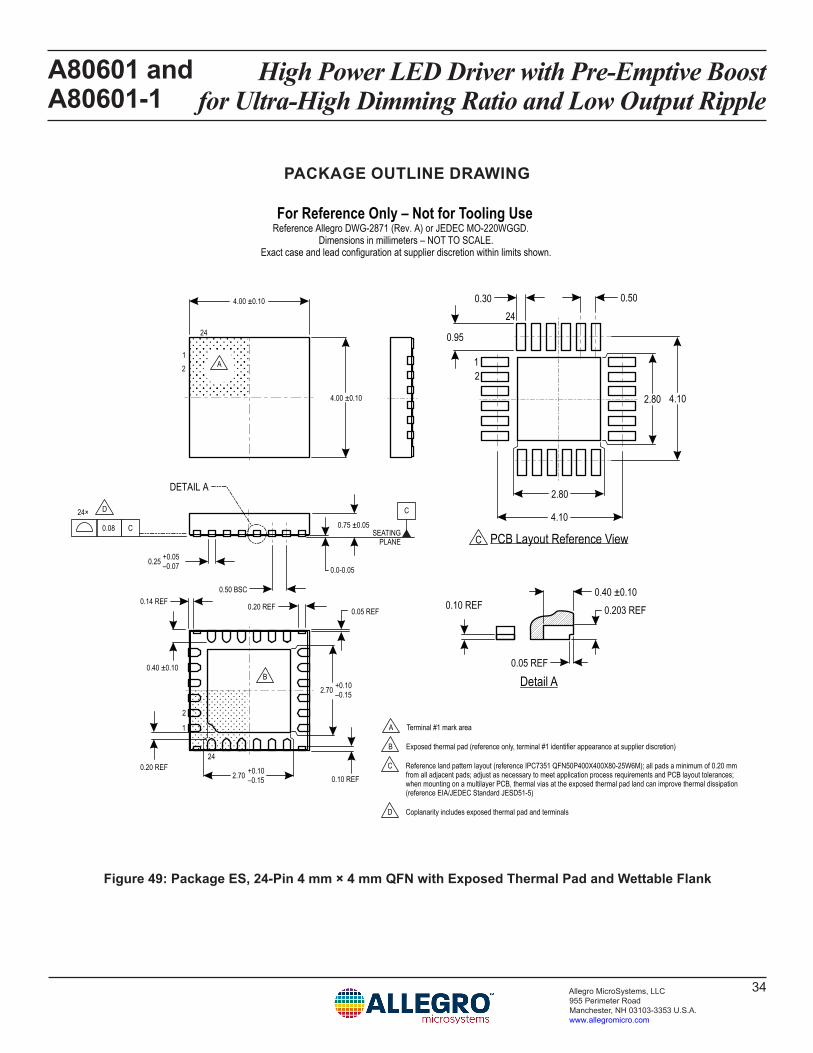
High Power LED Driver with Pre-Emptive Boost for Ultra-High Dimming Ratio and Low Output Ripple
A80601 and A80601-1
34Allegro MicroSystems, LLC 955 Perimeter Road Manchester, NH 03103-3353 U.S.A.www.allegromicro.com
PACKAGE OUTLINE DRAWING
Figure 49: Package ES, 24-Pin 4 mm × 4 mm QFN with Exposed Thermal Pad and Wettable Flank
Wide Input Voltage RangeHigh Efficiency Fault Tolerant LED DriverALT80600
Allegro MicroSystems, LLC115 Northeast CutoffWorcester, Massachusetts 01615-0036 U.S.A.1.508.853.5000; www.allegromicro.com
Package ES, 24-Contact QFN with Exposed Pad and Wettable Flank
For Reference Only – Not for Tooling UseReference Allegro DWG-2871 (Rev. A) or JEDEC MO-220WGGD.
Dimensions in millimeters – NOT TO SCALE.Exact case and lead configuration at supplier discretion within limits shown.
C
SEATINGPLANE
C0.08
24×
21
1
2
A
A
B
C
D
D
4.00 ±0.10
4.00 ±0.10
0.75 ±0.05
0.25
B
Terminal #1 mark area
Exposed thermal pad (reference only, terminal #1 identifier appearance at supplier discretion)
Reference land pattern layout (reference IPC7351 QFN50P400X400X80-25W6M); all pads a minimum of 0.20 mmfrom all adjacent pads; adjust as necessary to meet application process requirements and PCB layout tolerances;when mounting on a multilayer PCB, thermal vias at the exposed thermal pad land can improve thermal dissipation(reference EIA/JEDEC Standard JESD51-5)
Coplanarity includes exposed thermal pad and terminals
24
24
0.50 BSC
0.40 ±0.10
0.0-0.05
0.40 ±0.10
0.05 REF
0.10 REF 0.203 REF
Detail A
DETAIL A
0.05 REF0.20 REF
0.10 REF
0.14 REF
21
C
4.10
0.30 0.50
4.10
PCB Layout Reference View
0.95
24
2.80
2.80
2.70
2.70 +0.10–0.15
+0.10–0.15
0.20 REF
+0.05–0.07
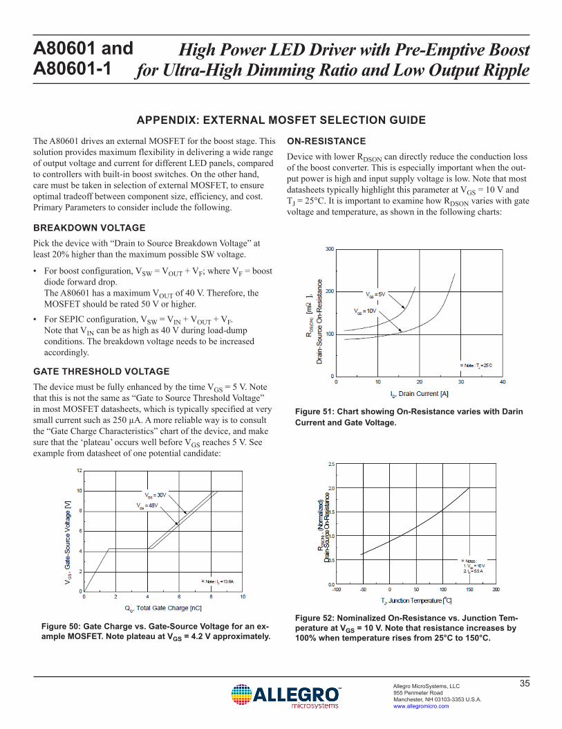
High Power LED Driver with Pre-Emptive Boost for Ultra-High Dimming Ratio and Low Output Ripple
A80601 and A80601-1
35Allegro MicroSystems, LLC 955 Perimeter Road Manchester, NH 03103-3353 U.S.A.www.allegromicro.com
APPENDIX: EXTERNAL MOSFET SELECTION GUIDE
The A80601 drives an external MOSFET for the boost stage. This solution provides maximum flexibility in delivering a wide range of output voltage and current for different LED panels, compared to controllers with built-in boost switches. On the other hand, care must be taken in selection of external MOSFET, to ensure optimal tradeoff between component size, efficiency, and cost. Primary Parameters to consider include the following.
BREAKDOWN VOLTAGEPick the device with “Drain to Source Breakdown Voltage” at least 20% higher than the maximum possible SW voltage.
• For boost configuration, VSW = VOUT + VF; where VF = boost diode forward drop. The A80601 has a maximum VOUT of 40 V. Therefore, the MOSFET should be rated 50 V or higher.
• For SEPIC configuration, VSW = VIN + VOUT + VF. Note that VIN can be as high as 40 V during load-dump conditions. The breakdown voltage needs to be increased accordingly.
GATE THRESHOLD VOLTAGEThe device must be fully enhanced by the time VGS = 5 V. Note that this is not the same as “Gate to Source Threshold Voltage” in most MOSFET datasheets, which is typically specified at very small current such as 250 µA. A more reliable way is to consult the “Gate Charge Characteristics” chart of the device, and make sure that the ‘plateau’ occurs well before VGS reaches 5 V. See example from datasheet of one potential candidate:
Figure 50: Gate Charge vs. Gate-Source Voltage for an ex-ample MOSFET. Note plateau at VGS = 4.2 V approximately.
ON-RESISTANCEDevice with lower RDSON can directly reduce the conduction loss of the boost converter. This is especially important when the out-put power is high and input supply voltage is low. Note that most datasheets typically highlight this parameter at VGS = 10 V and TJ = 25°C. It is important to examine how RDSON varies with gate voltage and temperature, as shown in the following charts:
Figure 51: Chart showing On-Resistance varies with Darin Current and Gate Voltage.
Figure 52: Nominalized On-Resistance vs. Junction Tem-perature at VGS = 10 V. Note that resistance increases by 100% when temperature rises from 25°C to 150°C.
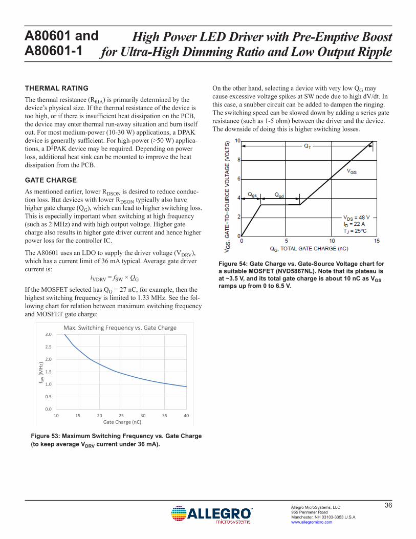
High Power LED Driver with Pre-Emptive Boost for Ultra-High Dimming Ratio and Low Output Ripple
A80601 and A80601-1
36Allegro MicroSystems, LLC 955 Perimeter Road Manchester, NH 03103-3353 U.S.A.www.allegromicro.com
THERMAL RATINGThe thermal resistance (RθJA) is primarily determined by the device’s physical size. If the thermal resistance of the device is too high, or if there is insufficient heat dissipation on the PCB, the device may enter thermal run-away situation and burn itself out. For most medium-power (10-30 W) applications, a DPAK device is generally sufficient. For high-power (>50 W) applica-tions, a D2PAK device may be required. Depending on power loss, additional heat sink can be mounted to improve the heat dissipation from the PCB.
GATE CHARGEAs mentioned earlier, lower RDSON is desired to reduce conduc-tion loss. But devices with lower RDSON typically also have higher gate charge (QG), which can lead to higher switching loss. This is especially important when switching at high frequency (such as 2 MHz) and with high output voltage. Higher gate charge also results in higher gate driver current and hence higher power loss for the controller IC.
The A80601 uses an LDO to supply the driver voltage (VDRV), which has a current limit of 36 mA typical. Average gate driver current is:
iVDRV = fSW × QG
If the MOSFET selected has QG = 27 nC, for example, then the highest switching frequency is limited to 1.33 MHz. See the fol-lowing chart for relation between maximum switching frequency and MOSFET gate charge:
0.0
0.5
1.0
1.5
2.0
2.5
3.0
10 15 20 25 30 35 40
f sw (M
Hz)
Gate Charge (nC)
Max. Switching Frequency vs. Gate Charge
Figure 53: Maximum Switching Frequency vs. Gate Charge (to keep average VDRV current under 36 mA).
On the other hand, selecting a device with very low QG may cause excessive voltage spikes at SW node due to high dV/dt. In this case, a snubber circuit can be added to dampen the ringing. The switching speed can be slowed down by adding a series gate resistance (such as 1-5 ohm) between the driver and the device. The downside of doing this is higher switching losses.
Figure 54: Gate Charge vs. Gate-Source Voltage chart for a suitable MOSFET (NVD5867NL). Note that its plateau is at ~3.5 V, and its total gate charge is about 10 nC as VGS ramps up from 0 to 6.5 V.

High Power LED Driver with Pre-Emptive Boost for Ultra-High Dimming Ratio and Low Output Ripple
A80601 and A80601-1
37Allegro MicroSystems, LLC 955 Perimeter Road Manchester, NH 03103-3353 U.S.A.www.allegromicro.com
For the latest version of this document, visit our website:www.allegromicro.com
Revision HistoryNumber Date Description
– March 4, 2019 Initial release
Copyright 2019, Allegro MicroSystems, LLCAllegro MicroSystems, LLC reserves the right to make, from time to time, such departures from the detail specifications as may be required to
permit improvements in the performance, reliability, or manufacturability of its products. Before placing an order, the user is cautioned to verify that the information being relied upon is current.
Allegro’s products are not to be used in any devices or systems, including but not limited to life support devices or systems, in which a failure of Allegro’s product can reasonably be expected to cause bodily harm.
The information included herein is believed to be accurate and reliable. However, Allegro MicroSystems, LLC assumes no responsibility for its use; nor for any infringement of patents or other rights of third parties which may result from its use.
Copies of this document are considered uncontrolled documents.