Embed Size (px)
Citation preview
High-side Power Distribution Switch
NCT3521U-A NCT3521U-2

NCT3521U-A/U-2
Publication Date: Nov., 2011 -I- Revision A1
-Table of Content-
1. GENERAL DESCRIPTION..................................................................................1 2. FEATURES .........................................................................................................1 3. APPLICATIONS ..................................................................................................2 4. PIN CONFIGURATION AND DESCRIPTION......................................................2 5. TYPICAL APPLICATION CIRCUIT .....................................................................3 6. BLOCK DIAGRAM...............................................................................................3 7. FUNCTIONAL DESCRIPTION ............................................................................4 8. ELECTRICAL CHARACTERISTICS....................................................................5 9. PACKAGE DIMENSION......................................................................................7 10. ORDERING INFORMATION .............................................................................11 11. TOP MARKING SPECIFICATION .....................................................................11 12. REVISION HISTORY.........................................................................................12
NCT3521U-A/U-2
Publication Date: Nov., 2011 -1- Revision A1
1. GENERAL DESCRIPTION The NCT3521 power switch is an integrated 80mΩ power switch IC designed for high-side
load switching applications.
The NCT3521 power switch operates with an input voltage range from 3.0 to 5.5V, making it
ideal for both 3V and 5V systems. The NCT3521 Power Switch also features an under-voltage
lock out which turns the switch off when an input under-voltage condition exists. The NCT3521
also have several protection that include current limiting, and thermal shutdown to prevent
catastrophic switch failure caused by increasing power dissipation when continuous heavy
loads or short circuit occurs. And a built-in charge pump is used to drive the N-channel
MOSFET that is free of parasitic body diode to eliminate any reversed current flow across the
switch when it is powered off. The NCT3521 features shutdown discharge function and soft-
start function, this makes the NCT3521 has slowly turn on and fast turn off features.
Its low quiescent current and small package is particularly suitable in battery-powered
equipment. In shutdown mode, the quiescent current decrease to less than 1uA.
2. FEATURES 80mΩ High-Side MOSFET Continues current up to 2A, Current trip threshold 2.5A Adjustable Soft-start (NCT3521U-2, SOT23-6 package) Operating Range from 2.7 to 5.5V 1.9mS Typical VOUT Turn-On Rise Time Under voltage Lockout 70uA Quiescent Supply Current 1uA Shutdown Current Active-High Enable Pin Fast response time at OCP Reverse Input-Output Voltage Protection Adjustable Shutdown Discharge Slowly turn on and fast turn off TSOT-23-5/ SOT-23-6 Lead Free (ROHS Compliant) and Halogen Free Package

NCT3521U-A/U-2
3. APPLICATIONS High-Side Power Protection Switch Hot Plug-Powered Hubs Battery-Charger Circuits
4. PIN CONFIGURATION AND DESCRIPTION
NCT3521U-A (Top View)
EN
GND
OUT
5 SS
DIS
IN
2
3
1
4
6
DIS
IN
EN
GND
OUT
3
1
2
4
5
NCT3521U-2 (Top View)
3521 U-2
3521 U-A
PIN NAME I/O FUNCTION
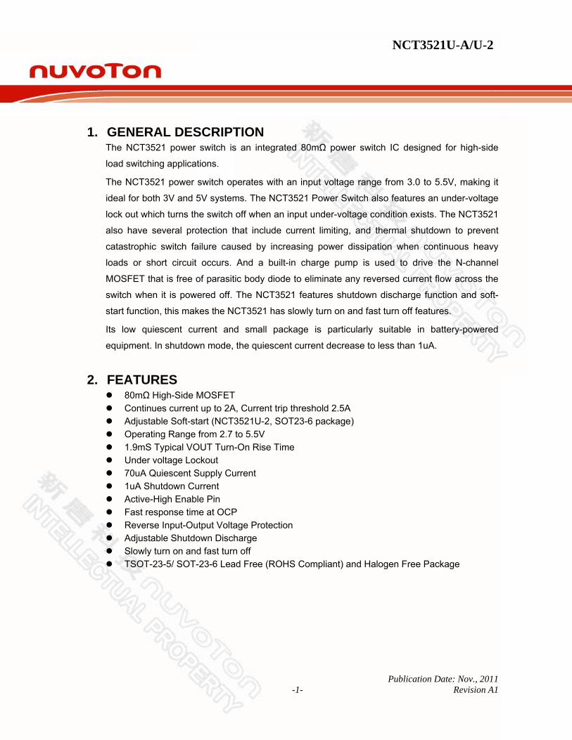
1 1 OUT O Output Voltage. This pin is the N-MOSFET Source that delivers the voltage to output. Connecting a 0.1uF or greater ceramic capacitor from this pin to GND as close to the chip as possible.
2 2 GND GND.
3 3 EN I Enable. High enable. Pulling this pin to the logic low will disable the chip.
4 4 DIS I Discharge. Drain of internal N-MOSFET. This pin will active when chip is disabled. By connecting a resistor from DIS to OUT pin, the voltage of OUT can be sink from this pin when chip is disabled.
5 SS I Soft-start. Placing a capacitor from this pin to GND can set the ramp up time.
6 5 IN I
Input Voltage. This pin is the N-MOSFET Drain that supplies output current and also supplies operating current for the chip. Connecting a 0.1uF or greater ceramic capacitor from this pin to GND as close to the chip as possible.
Publication Date: Nov., 2011 -2- Revision A1
NCT3521U-A/U-2
5. TYPICAL APPLICATION CIRCUIT
Publication Date: Nov., 2011 -3- Revision A1
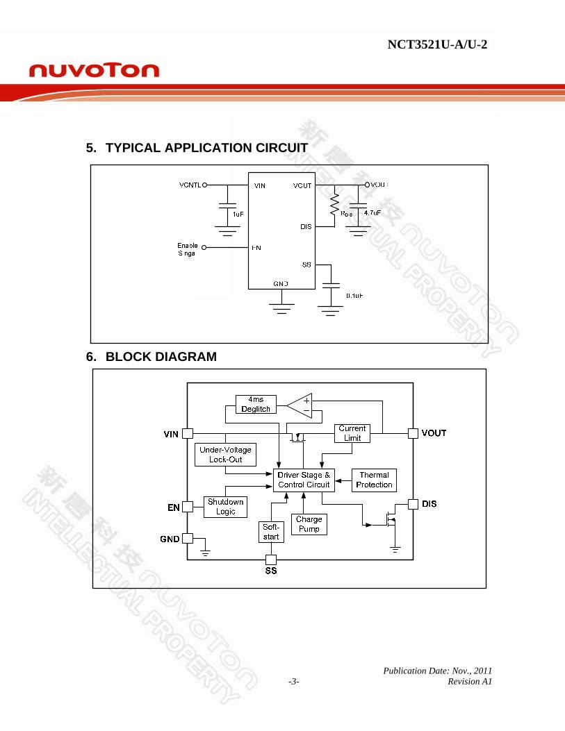
6. BLOCK DIAGRAM

NCT3521U-A/U-2
Publication Date: Nov., 2011 -4- Revision A1
7. FUNCTIONAL DESCRIPTION 7.1 Product Introduction The NCT3521 power switch is a N-Channel MOSFET power switches designed for high-side load switching applications. Once turned on, the soft-start circuitry is activated and the output current is ramped up with linear until it reaches the level required for the output load condition. The typical soft-start time is 1.9mS, it can be changed by capacitor connected in SS pin. 7.2 Soft-start The NCT3521 built-in soft-start function to reduce the inrush current and eliminate the voltage drop at Vin supply voltage when enabling. The soft-start interval is typically 1.9ms. The soft-start can be adjusted by an external soft-start capacitor connected from SS pin to GND. 7.3 Under Voltage Lockout UVLO (under voltage lockout) prevents the output MOSFET from turning on until VIN exceeds 2.6V typically. After the switch turns on, if the voltage drops below 2.3V typically, UVLO shuts off the output MOSFET. Built-in hysteresis prevents unwanted turn on/off due to input voltage drop from large current surges. 7.4 Enable The NCT3521 is disabled when the EN pin is in the logic low condition. During disabled, The supply current reduce to below 1uA typically. The voltage level of enable pin is also compatible with both TTL and CMOS logic voltage levels. This pin can’t floating, please connect logic high or logic low. 7.5 Over Current Limit The NCT3521 contains an independent current limit and the short circuit current protection to prevent unexpected applications. The current limit monitors and controls the Internal MOSFET gate voltage, limiting the output current to higher than 2A typical. The output can be shorted to ground indefinitely without damaging the part. 7.6 Thermal-Shutdown Protection Thermal protection limits power dissipation to prevent IC over temperature exceeds 150, the over-temperature protection circuit starts the thermal shutdown function and turns the pass transistor off. The pass transistor turns on again after the junction temperature is falling 50 (junction temperature
≦100). 7.7 Application information
Input Capacitor and Output Capacitor A minimum of 1uF ceramic capacitor is recommended to be placed directly next to the Vin pin. The Bypass capacitor should be placed as close as possible to the VIN pin to be effective in minimizing transients on the input.
Noise Immunity In very electrically noisy environments, it is recommended that 0.1uF ceramic capacitors be placed from IN to GND and OUT to GND as close to device pins as possible.

NCT3521U-A/U-2
Publication Date: Nov., 2011 -5- Revision A1
8. ELECTRICAL CHARACTERISTICS
8.1 Absolute Maximum Ratings PARAMETER RATING UNIT
Input Supply Voltage -0.3 to 6V V
Other Pins -0.3 to 6V V
Power Dissipation, PD @ TA=25 Internal Limited W
Package Thermal Resistance, TSOT23-5/SOT23-6, θJA 240 /W
Storage Temperature -50 to 150
Junction Temperature 150
Human Body Mode 2 kV
Machine Mode 200 V ESD Protection
Latch-up 100 mA
Note: Exposure to conditions beyond those listed under Absolute Maximum Ratings may adversely affect the life and reliability of the device.
8.2 Recommended Operating Conditions PARAMETER RATING UNIT
Supply Voltage VIN 2.7 to 5.5 V
Operating Temperature -40 to 85
Junction Temperature -40 to 125
Note: Limits are 100% production tested at 25°C. Limits over the operating temperature range are guaranteed through correlation using Statistical Quality Control (SQC) methods.
NCT3521U-A/U-2
Publication Date: Nov., 2011 -6- Revision A1
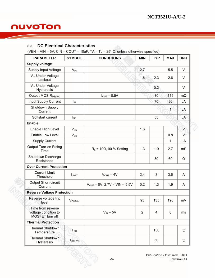
8.3 DC Electrical Characteristics (VEN = VIN = 5V, CIN = COUT = 10uF, TA = TJ = 25° C, unless otherwise specified)
PARAMETER SYMBOL CONDITIONS MIN TYP MAX UNITSupply voltage Supply Input Voltage VIN 2.7 5.5 V
VIN Under Voltage Lockout 1.6 2.3 2.6 V
VIN Under Voltage Hysteresis 0.2 V
Output MOS RDS(ON) IOUT = 0.5A 80 115 mΩ
Input Supply Current IIN 70 80 uA
Shutdown Supply Current 1 uA
Softstart current ISS 55 uA
Enable Enable High Level VEN 1.6 V
Enable Low Level VSD 0.8 V
Supply Current 1 uA
Output Turn-on Rising Time RL = 10Ω, 90 % Setting 1.3 1.9 2.7 mS
Shutdown Discharge Resistance 30 60 Ω
Over Current Protection Current Limit
Threshold ILIMIT VOUT = 4V 2.4 3 3.6 A
Output Short-circuit Current VOUT = 0V, 2.7V < VIN < 5.5V 0.2 1.3 1.9 A
Reverse Voltage Protection Reverse voltage trip
level VOUT-IN 95 135 190 mV
Time from reverse voltage condition to MOSFET turn off
VIN = 5V 2 4 8 ms
Thermal Protection Thermal Shutdown
Temperature TSD 150
Thermal Shutdown Hysteresis TSDHYS 50

NCT3521U-A/U-2
9. TYPICAL OPERATING WAVEFORMS (VIN = VEN = 5V, COUT = 1uF, CIN = 1uF, TA = 25 , unless otherwise specified)
Publication Date: Nov., 2011 -7- Revision A1
Figure 1. Turn-on and Rising-time Figure 2. Turn-off and Falling-time Figure 3. Current Limit Trip and Current Limit
VIN = 4V
Figure 4. Short-circuit, device enable into short
Figure 6. Over-temperature Protection Figure 5. Short-circuit, Normal operation
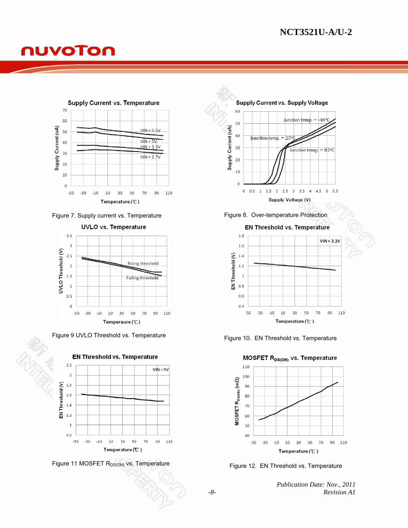
NCT3521U-A/U-2
Figure 8. Over-temperature Protection Figure 7. Supply current vs. Temperature Figure 9 UVLO Threshold vs. Temperature Figure 10. EN Threshold vs. Temperature
Publication Date: Nov., 2011 -8- Revision A1
Figure 11 MOSFET RDS(ON) vs. Temperature Figure 12. EN Threshold vs. Temperature
NCT3521U-A/U-2
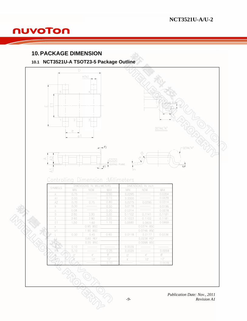
10. PACKAGE DIMENSION 10.1 NCT3521U-A TSOT23-5 Package Outline
Publication Date: Nov., 2011 -9- Revision A1

NCT3521U-A/U-2
10.2 NCT3521U-2 SOT23-6 Package Outline
Publication Date: Nov., 2011 -10- Revision A1

NCT3521U-A/U-2
TAPING SPECIFICATION
TSOT23-5/SOT23-5/ SOT23-6 Package
11. ORDERING INFORMATION PART NUMBER SUPPLIED AS PACKAGE TYPE PRODUCTION FLOW
NCT3521U-A TSOT23-5 (Green package)
NCT3521U-2
T Shape : 3,000 units/T&R SOT23-6 (Green package)
Commercial, 0 to +70
12. TOP MARKING SPECIFICATION
1st Line: 21AXX
Publication Date: Nov., 2011 -11- Revision A1
1st Line: 21AXX
21: NCT3521 21: NCT3521 A : Internal Use Only A : Internal Use Only XX: Assembly Date Code (Week) XX: Assembly Date Code (Week)
21AXX
TSOT23-5
21AXX
SOT23-6
NCT3521U-A/U-2
13. REVISION HISTORY
VERSION DATE PAGE DESCRIPTION
A1 11/07/2011 All New Create
Important Notice Nuvoton Products are neither intended nor warranted for usage in systems or equipment, any malfunction or failure of which may cause loss of human life, bodily injury or severe property damage. Such applications are deemed, “Insecure Usage”.
Insecure usage includes, but is not limited to: equipment for surgical implementation, atomic energy control instruments, airplane or spaceship instruments, the control or operation of dynamic, brake or safety systems designed for vehicular use, traffic signal instruments, all types of safety devices, and other applications intended to support or sustain life.
All Insecure Usage shall be made at customer’s risk, and in the event that third parties lay claims to Nuvoton as a result of customer’s Insecure Usage, customer shall indemnify the damages and liabilities thus incurred by Nuvoton.
Publication Date: Nov., 2011 -12- Revision A1