Embed Size (px)
Citation preview
122
International Journal of Future Computer and Communication, Vol. 4, No. 2, April 2015
Abstract—The advantages of X-ray inspection are extensive
in scope due to the ability of X-rays to see through packages
including heat sinks, welds, encapsulation, and metallic
shielding to reveal obscured connections and identify potential
quality non-destructive issues. Many assembly line
manufacturers rely on real-time X-ray technology to evaluate
solder joint integrity for BGAs and other leadless packages that
cannot be inspected by conventional vision systems. X-ray
inspection is particularly beneficial to applications that involve
advanced surface-mount packaging technologies such as Ball
Grid Array (BGA) used for integrated circuits. This paper
proposes a method that relies on computer vision and image
processing techniques that inspects each ball image of a BGA
chip and indicates the faulty balls for further assessment. The
defective balls that are typically circular change into elongated
or elliptical shape. Therefore, it exploits the use of the basic
geometric distinction between a circle (perfect soldered ball)
and an ellipse or any other shape (ball with reshaped solder
joint). A contour analysis method is defined in this paper in
terms of the angle changes that occur along the outline profile of
a solder joint by moving three equal distant points located on
the border. This angle change is plotted to detect the faulty ball
joints.
Index Terms—BGA, shape analysis, solder joints, X-ray
techniques.
I. INTRODUCTION
Computer vision is a process to locate and recognize
objects in digital images. It involves techniques from image
processing, pattern recognition and artificial intelligence.
Computer vision has been used in diverse areas of
applications. One such important area is in the field of on-line
or off-line visual inspection systems of microscopic
applications [1]–[3].
X-ray inspection systems are widely used by electronics
and SMT (surface-mount technology) manufacturers to
control the quality of the hidden solder joints of BGA, wafer
bonding defects, FCA (flip-chip assemblies), CSP (chip scale
packages), QFN (quad flat no lead), and flip-chip
components.
X-ray image processing, fault detection, and failure
analysis tools provide the ability to quantify and fine-tune
manufacturing processes, improve quality, yield, reduce
scrap, and decrease warranty returns. X-ray examination has
become an exceptional tool for process improvement, design
evaluation, and quality assessment. To be brief, having X-ray
inspection capability can positively affect the entire lifecycle
Manuscript received September 9, 2014; revised December 23, 2014.
The authors are with the Department of Electrical Engineering, United
Arab Emirates University, P. O. Box: 15551, Al Ain, United Arab Emirates
(e-mail: [email protected], [email protected]).
of a product [4].
X-ray imaging is beneficial because it allows the
inspection of component interiors and multiple layers of the
board simultaneously. This viewing allows the detection of
faults such as broken internal traces, voids in solder joints,
and other flaws that would possibly go undetected by
inspection schemes that use visible light or infrared light.
Although, visual inspection is monotonous and faults are
difficult to detect using visible light however, it is important
to note that the idea is not intended to substitute the human's
function but to make it easier for the casual user to identify
the suspect areas (solder joints) for further modification. It
merely simplifies the visualization of the suspect balls and
allows the user to inspect them individually.
BGA packages are used to permanently-mount devices
such as microprocessors. One of the major causes of
defective BGA chipsets is the improper solder joints between
adjacent balls. This causes undesired short between the
affected balls and renders the chip dysfunctional. Detecting
such flaws are currently relied on a human visualization of an
X-ray image or tested electrically of the undermined chip. If
the chip has several hundreds of balls and the solder joints are
marginal, then it may be undetected by the casual observer.
The weakness of manual inspection is the large amount of
time required that results in the fatigue of the operator and
decrease in the efficiency of work.
Electrical testing need probe holes on the chipboard
reducing the advantage of component miniaturization. Such
techniques will be unreliable in the future when chips will
have even more leads and spaced even more closely. These
methods also have the shortcoming that they do not provide
any quantitative information about why joints failed [5].
Other methods and equipments applied for electronic
failure inspections are: optical microscopy, cross sectioning,
BGA DYE&PRY test (destructive analysis method), shear
test, scanning electron microscopy, X-ray fluorescent
spectroscopy, de-capsulation, scanning acoustic microscopy,
etc.
Typical solder joint failures detected by these techniques
included with the X-ray are: wetting problem of cut surfaces,
voiding, broken solder joint, shorts or bridging, insufficient
through-hole solder joints, detection of de-elimination,
missing part or connection points, misalignment,
unacceptable size and shape variations in solder volume,
poor co-planarity, etc. [6], [7].
Artificial neural network algorithms have also been
applied in a variety of X-ray application domains. A
QuickCog PC system is applied and adapted to advanced
problems in electronics manufacturing. An automated X-ray
image inspection system in electronics manufacturing can be
Identification of Faulty BGA Solder Joints in X-Ray
Images
Mohammad S. Laghari, Member, IACSIT and Qurban A. Memon
10.7763/IJFCC.2015.V4.369DOI:
123
International Journal of Future Computer and Communication, Vol. 4, No. 2, April 2015
performed with advanced sensor technology [8].
Computer vision and image processing techniques have
been applied that detects each ball of the BGA chip and flags
the suspect balls for further evaluation. Techniques such as
Connected Component Analysis and K-L transformation
were used to distinguish between geometric shapes of circle
and ellipse [9].
The contour analysis method described in the paper is
based on the perimeter data of the ball joint. It is defined in
terms of the angle changes that occurs along the perimeter of
a ball joint image by moving three adjacent equidistant points
located on the border. This angle change is plotted on a graph
and faulty ball joints are flagged when the plots exceed a
threshold value.
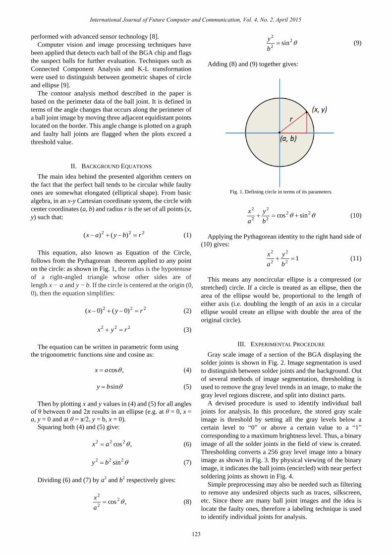
II. BACKGROUND EQUATIONS
The main idea behind the presented algorithm centers on
the fact that the perfect ball tends to be circular while faulty
ones are somewhat elongated (elliptical shape). From basic
algebra, in an x-y Cartesian coordinate system, the circle with
center coordinates (a, b) and radius r is the set of all points (x,
y) such that:
222 )()( rbyax (1)
This equation, also known as Equation of the Circle,
follows from the Pythagorean theorem applied to any point
on the circle: as shown in Fig. 1, the radius is the hypotenuse
of a right-angled triangle whose other sides are of
length x − a and y − b. If the circle is centered at the origin (0,
0), then the equation simplifies:
222 )0()0( ryx (2)
222 ryx (3)
The equation can be written in parametric form using
the trigonometric functions sine and cosine as:
,cosax (4)
sinby (5)
Then by plotting x and y values in (4) and (5) for all angles
of θ between 0 and 2π results in an ellipse (e.g. at θ = 0, x =
a, y = 0 and at θ = π/2, y = b, x = 0).
Squaring both (4) and (5) give:
,cos222 ax (6)
222 sinby (7)
Dividing (6) and (7) by a2 and b2 respectively gives:
,cos2
2
2
a
x (8)
2
2
2
sinb
y (9)
Adding (8) and (9) together gives:
Fig. 1. Defining circle in terms of its parameters.
22
2
2
2
2
sincos b
y
a
x (10)
Applying the Pythagorean identity to the right hand side of
(10) gives:
12
2
2
2
b
y
a
x (11)
This means any noncircular ellipse is a compressed (or
stretched) circle. If a circle is treated as an ellipse, then the
area of the ellipse would be, proportional to the length of
either axis (i.e. doubling the length of an axis in a circular
ellipse would create an ellipse with double the area of the
original circle).
III. EXPERIMENTAL PROCEDURE
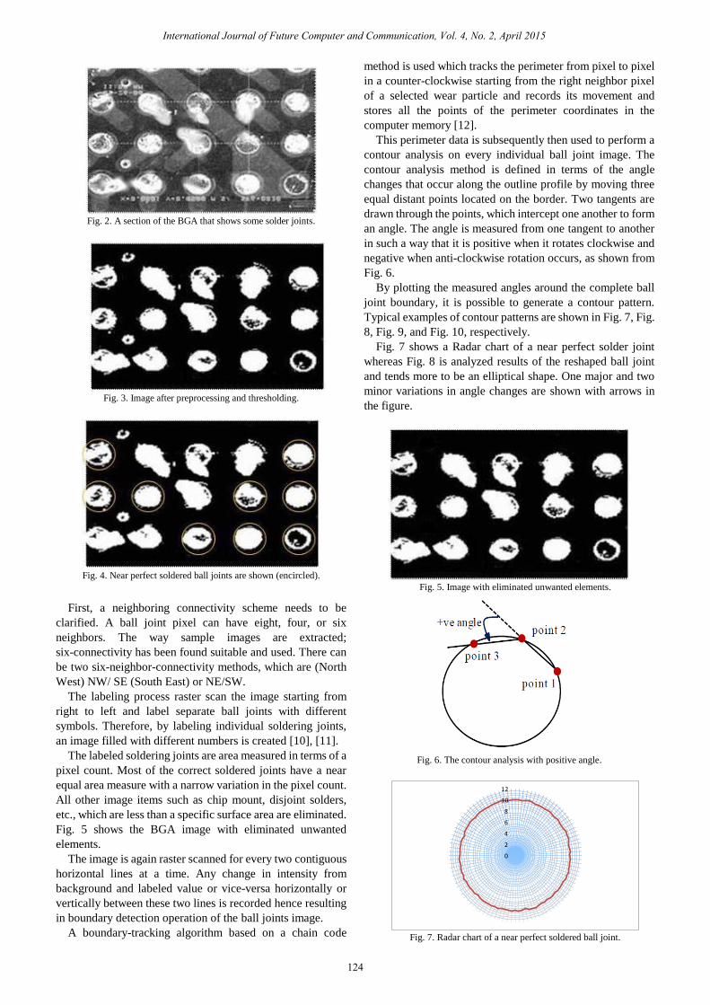
Gray scale image of a section of the BGA displaying the
solder joints is shown in Fig. 2. Image segmentation is used
to distinguish between solder joints and the background. Out
of several methods of image segmentation, thresholding is
used to remove the gray level trends in an image, to make the
gray level regions discrete, and split into distinct parts.
A devised procedure is used to identify individual ball
joints for analysis. In this procedure, the stored gray scale
image is threshold by setting all the gray levels below a
certain level to “0” or above a certain value to a “1”
corresponding to a maximum brightness level. Thus, a binary
image of all the solder joints in the field of view is created.
Thresholding converts a 256 gray level image into a binary
image as shown in Fig. 3. By physical viewing of the binary
image, it indicates the ball joints (encircled) with near perfect
soldering joints as shown in Fig. 4.
Simple preprocessing may also be needed such as filtering
to remove any undesired objects such as traces, silkscreen,
etc. Since there are many ball joint images and the idea is
locate the faulty ones, therefore a labeling technique is used
to identify individual joints for analysis.
124
International Journal of Future Computer and Communication, Vol. 4, No. 2, April 2015
Fig. 2. A section of the BGA that shows some solder joints.
Fig. 3. Image after preprocessing and thresholding.
Fig. 4. Near perfect soldered ball joints are shown (encircled).
First, a neighboring connectivity scheme needs to be
clarified. A ball joint pixel can have eight, four, or six
neighbors. The way sample images are extracted;
six-connectivity has been found suitable and used. There can
be two six-neighbor-connectivity methods, which are (North
West) NW/ SE (South East) or NE/SW.
The labeling process raster scan the image starting from
right to left and label separate ball joints with different
symbols. Therefore, by labeling individual soldering joints,
an image filled with different numbers is created [10], [11].
The labeled soldering joints are area measured in terms of a
pixel count. Most of the correct soldered joints have a near
equal area measure with a narrow variation in the pixel count.
All other image items such as chip mount, disjoint solders,
etc., which are less than a specific surface area are eliminated.
Fig. 5 shows the BGA image with eliminated unwanted
elements.
The image is again raster scanned for every two contiguous
horizontal lines at a time. Any change in intensity from
background and labeled value or vice-versa horizontally or
vertically between these two lines is recorded hence resulting
in boundary detection operation of the ball joints image.
A boundary-tracking algorithm based on a chain code
method is used which tracks the perimeter from pixel to pixel
in a counter-clockwise starting from the right neighbor pixel
of a selected wear particle and records its movement and
stores all the points of the perimeter coordinates in the
computer memory [12].
This perimeter data is subsequently then used to perform a
contour analysis on every individual ball joint image. The
contour analysis method is defined in terms of the angle
changes that occur along the outline profile by moving three
equal distant points located on the border. Two tangents are
drawn through the points, which intercept one another to form
an angle. The angle is measured from one tangent to another
in such a way that it is positive when it rotates clockwise and
negative when anti-clockwise rotation occurs, as shown from
Fig. 6.
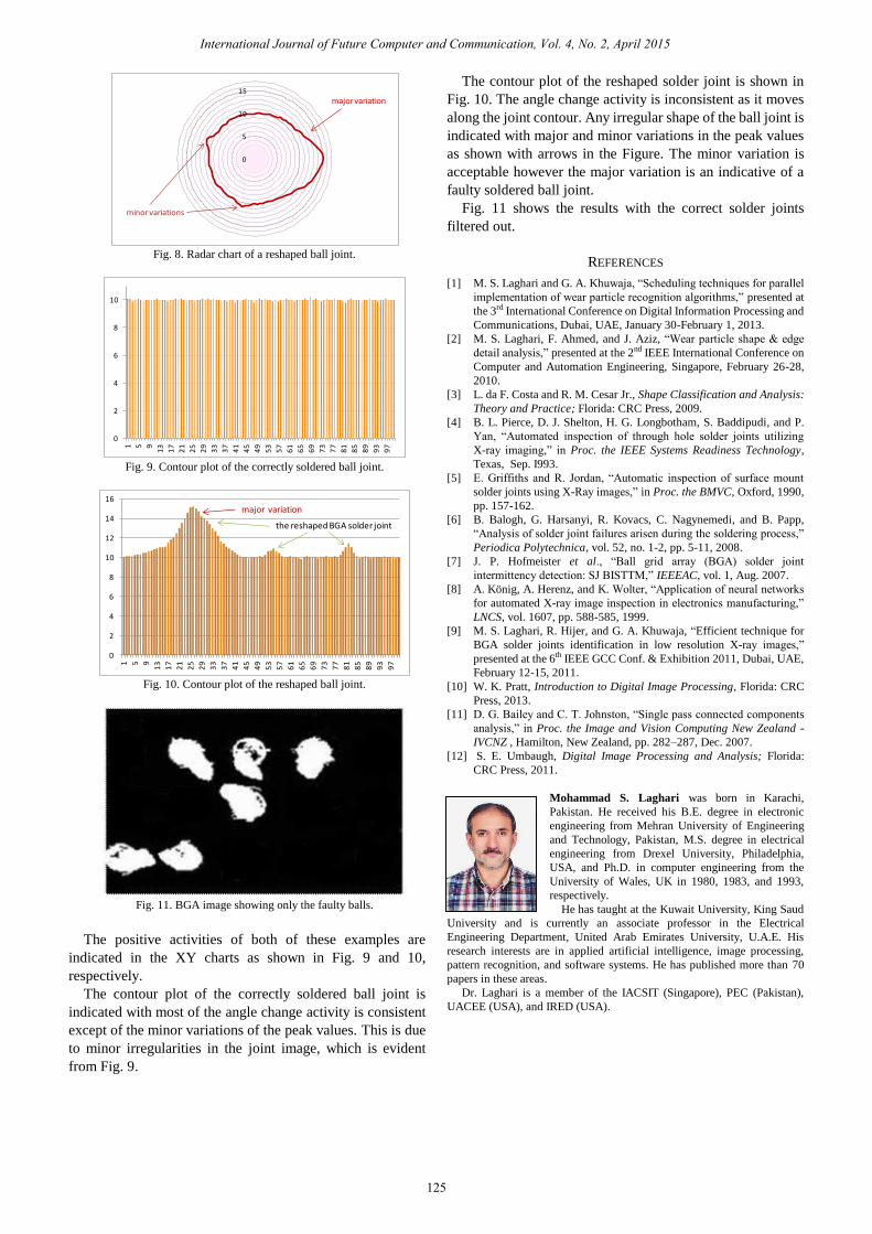
By plotting the measured angles around the complete ball
joint boundary, it is possible to generate a contour pattern.
Typical examples of contour patterns are shown in Fig. 7, Fig.
8, Fig. 9, and Fig. 10, respectively.
Fig. 7 shows a Radar chart of a near perfect solder joint
whereas Fig. 8 is analyzed results of the reshaped ball joint
and tends more to be an elliptical shape. One major and two
minor variations in angle changes are shown with arrows in
the figure.
Fig. 5. Image with eliminated unwanted elements.
Fig. 6. The contour analysis with positive angle.
0
2
4
6
8
10
12
Fig. 7. Radar chart of a near perfect soldered ball joint.
125
International Journal of Future Computer and Communication, Vol. 4, No. 2, April 2015
0
5
10
15
minor variations
major variation
Fig. 8. Radar chart of a reshaped ball joint.
0
2
4
6
8
10
1 5 9
13
17
21
25
29
33
37
41
45
49
53
57
61
65
69
73
77
81
85
89
93
97
Fig. 9. Contour plot of the correctly soldered ball joint.
0
2
4
6
8
10
12
14
16
1 5 9
13
17
21
25
29
33
37
41
45
49
53
57
61
65
69
73
77
81
85
89
93
97
the reshaped BGA solder joint
major variation
Fig. 10. Contour plot of the reshaped ball joint.
Fig. 11. BGA image showing only the faulty balls.
The positive activities of both of these examples are
indicated in the XY charts as shown in Fig. 9 and 10,
respectively.
The contour plot of the correctly soldered ball joint is
indicated with most of the angle change activity is consistent
except of the minor variations of the peak values. This is due
to minor irregularities in the joint image, which is evident
from Fig. 9.
The contour plot of the reshaped solder joint is shown in
Fig. 10. The angle change activity is inconsistent as it moves
along the joint contour. Any irregular shape of the ball joint is
indicated with major and minor variations in the peak values
as shown with arrows in the Figure. The minor variation is
acceptable however the major variation is an indicative of a
faulty soldered ball joint.
Fig. 11 shows the results with the correct solder joints
filtered out.
REFERENCES
[1] M. S. Laghari and G. A. Khuwaja, “Scheduling techniques for parallel
implementation of wear particle recognition algorithms,” presented at
the 3rd International Conference on Digital Information Processing and
Communications, Dubai, UAE, January 30-February 1, 2013.
[2] M. S. Laghari, F. Ahmed, and J. Aziz, “Wear particle shape & edge
detail analysis,” presented at the 2nd IEEE International Conference on
Computer and Automation Engineering, Singapore, February 26-28,
2010.
[3] L. da F. Costa and R. M. Cesar Jr., Shape Classification and Analysis:
Theory and Practice; Florida: CRC Press, 2009.
[4] B. L. Pierce, D. J. Shelton, H. G. Longbotham, S. Baddipudi, and P.
Yan, “Automated inspection of through hole solder joints utilizing
X-ray imaging,” in Proc. the IEEE Systems Readiness Technology,
Texas, Sep. I993.
[5] E. Griffiths and R. Jordan, “Automatic inspection of surface mount
solder joints using X-Ray images,” in Proc. the BMVC, Oxford, 1990,
pp. 157-162.
[6] B. Balogh, G. Harsanyi, R. Kovacs, C. Nagynemedi, and B. Papp,
“Analysis of solder joint failures arisen during the soldering process,”
Periodica Polytechnica, vol. 52, no. 1-2, pp. 5-11, 2008.
[7] J. P. Hofmeister et al., “Ball grid array (BGA) solder joint
intermittency detection: SJ BISTTM,” IEEEAC, vol. 1, Aug. 2007.
[8] A. König, A. Herenz, and K. Wolter, “Application of neural networks
for automated X-ray image inspection in electronics manufacturing,”
LNCS, vol. 1607, pp. 588-585, 1999.
[9] M. S. Laghari, R. Hijer, and G. A. Khuwaja, “Efficient technique for
BGA solder joints identification in low resolution X-ray images,”
presented at the 6th IEEE GCC Conf. & Exhibition 2011, Dubai, UAE,
February 12-15, 2011.
[10] W. K. Pratt, Introduction to Digital Image Processing, Florida: CRC
Press, 2013.
[11] D. G. Bailey and C. T. Johnston, “Single pass connected components
analysis,” in Proc. the Image and Vision Computing New Zealand -
IVCNZ , Hamilton, New Zealand, pp. 282–287, Dec. 2007.
[12] S. E. Umbaugh, Digital Image Processing and Analysis; Florida:
CRC Press, 2011.
Mohammad S. Laghari was born in Karachi,
Pakistan. He received his B.E. degree in electronic
engineering from Mehran University of Engineering
and Technology, Pakistan, M.S. degree in electrical
engineering from Drexel University, Philadelphia,
USA, and Ph.D. in computer engineering from the
University of Wales, UK in 1980, 1983, and 1993,
respectively.
He has taught at the Kuwait University, King Saud
University and is currently an associate professor in the Electrical
Engineering Department, United Arab Emirates University, U.A.E. His
research interests are in applied artificial intelligence, image processing,
pattern recognition, and software systems. He has published more than 70
papers in these areas.
Dr. Laghari is a member of the IACSIT (Singapore), PEC (Pakistan),
UACEE (USA), and IRED (USA).
Author’s formal
photo


![de partido a su piscina… - BINDER · Tipo BGA 160 BGA 215 BGA 275 BGA 320 BGA 430 BGA 550 BGA 600 BGA 1200 Tensión de conexión [VAC] 230 230 230 230 230 230 230 230 Rango de frecuencia](https://img.pdfslide.net/doc/110x75/5c132e8509d3f26c7c8c5e0d/de-partido-a-su-piscina-binder-tipo-bga-160-bga-215-bga-275-bga-320-bga-430.jpg)