Embed Size (px)
Citation preview
Open Cores IEEE 1149.1 Test Access Port 1/30/2004
http://www.opencores.org/
Copyright (C) 2001 - 2004 OPENCORES.ORG and Authors.
This document is free; you can redistribute it and/or modify it under the terms of the GNU General Public License as published by the Free Software Foundation; either version 2 of the License, or (at your option) any later version.
This document is distributed in the hope that it will be useful, but WITHOUT ANY WARRANTY; without even the implied warranty of MERCHANTABILITY or FITNESS FOR A PARTICULAR PURPOSE. See the GNU General Public License for more details.
Rev 2.0 Page 2 of 19
Open Cores IEEE 1149.1 Test Access Port 1/30/2004
http://www.opencores.org/
Revision History Rev. Date Author Description 0.1 02/02/01 Igor Mohor First Draft 0.2 05/04/01 IM Trace port added 0.3 16/04/01 IM WP and BP number changed, trace modified 0.4 01/05/01 IM Title changed, DEBUG instruction added, scan
chains changed, IO ports changed 0.5 05/05/01 IM TSEL and QSEL register changed 0.6 06/05/01 IM Ports connected to the OpenRISC changed 0.7 14/05/01 IM MODER register changed, trace scan chain
changed; SSEL register added 0.8 18/05/01 IM RESET bit and signal added; STALLR changed to
RISCOP 0.9 23/05/01 IM RISC changed to OpenRISC; WISHBONE
interface added, SPR and memory access added 0.10 01/06/01 IM Meaning of Instruction status and Load/store
status changed in all registers; more details added to Appendix A
0.11 10/09/01 IM Register and OpenRISC scan chain operation changed
1.0 19/09/01 IM Some registers deleted 1.1 15/10/01 IM WISHBONE interface added; RISC Stall signal is
set by breakpoint and reset by writing 0 to RISCOP register
1.2 03/12/01 IM Chain length changed so additional CRC checking can be performed
1.3 21/01/02 Jeanne Wiegelmann
Document revised.
1.4 07/05/02 IM Register MONCNTL added. 1.5 10/10/02 IM WISHBONE Scan Chain changed to show state of
the access. 1.6 06/11/02 IM TRST_PAD_I changed from active low signal to
active low signal. 1.7 23/09/03 Simon Srot Mutliple CPU support added, WB 16-bit and 8-bit
access possible through WBCNTL register use. 2.0 30/01/04 IM JTAG and debug interface split into two different
cores (and documents).
Rev 2.0 Page 3 of 19
Open Cores IEEE 1149.1 Test Access Port 1/30/2004
http://www.opencores.org/
Contents 1..............................................................................................................................................................7
INTRODUCTION................................................................................................................................7
2..............................................................................................................................................................8
IO PORTS.............................................................................................................................................8 2.1 JTAG PORTS .............................................................................................................................................................. 8 2.2 DEBUG PORTS............................................................................................................................................................. 8
3............................................................................................................................................................10
REGISTERS.......................................................................................................................................10 3.1 REGISTERS LIST........................................................................................................................................................ 10 3.2 IR (INSTRUCTION REGISTER) .................................................................................................................................... 11 3.3 IDCODE REGISTER .................................................................................................................................................. 11
4............................................................................................................................................................12
OPERATION .....................................................................................................................................12 4.2 JTAG INTERFACE AND THE TAP CONTROLLER........................................................................................................ 12 4.2.1 EXTEST (IR=0000)............................................................................................................................................. 13 4.2.2 SAMPLE/PRELOAD (IR=0001) ....................................................................................................................... 13 4.2.3. IDCODE (IR=0010) ........................................................................................................................................... 13 4.2.4 DEBUG (IR=1000) .............................................................................................................................................. 14 4.2.5 MBIST (IR=1001)................................................................................................................................................ 14 4.2.6 BYPASS (IR=1111) ............................................................................................................................................. 14 4.3 SCAN CHAINS ........................................................................................................................................................... 14 4.3.1 ID Scan Chain...................................................................................................................................................... 16 4.3.2 Debug Scan Chain ............................................................................................................................................... 16 4.3.3 Global BS (Boundary Scan) Chain .................................................................................................................... 16 4.3.4 Memory BIST Scan Chain ................................................................................................................................. 16
5............................................................................................................................................................17
ARCHITECTURE.............................................................................................................................17 5.1 TAP CONTROLLER ................................................................................................................................................... 18 5.1 TAP CONTROLLER IN THE SYSTEM ........................................................................................................................... 19
Rev 2.0 Page 4 of 19
Open Cores IEEE 1149.1 Test Access Port 1/30/2004
http://www.opencores.org/
List of Figures Figure 1: TAP Controller ....................................................................................................................18
Figure 2: Complete System ................................................................................................................19
Rev 2.0 Page 5 of 19
Open Cores IEEE 1149.1 Test Access Port 1/30/2004
http://www.opencores.org/
List of Tables Table 1: JTAG Ports .............................................................................................................................8
Table 2: Debug Ports ...........................................................................................................................9
Table 3: Register List .........................................................................................................................10
Table 4: IR Register ...........................................................................................................................11
Table 5: IDCODE Register ...............................................................................................................11
Rev 2.0 Page 6 of 19
Open Cores IEEE 1149.1 Test Access Port 1/30/2004
http://www.opencores.org/
1 Introduction
The JTAG TAP controller used for development purposes (Boundary Scan testing, Memory BIST and debugging) and is as such an interface between the processor(s), peripheral cores, and any commercial debugger/emulator or BS testing device. The external debugger or BS tester connects to the core via a fully IEEE 1149.1 compatible JTAG port. This core connects to the debug interface that is interface to the cores that are being debugged (see “dbg_interface” on Opencores web page).
Rev 2.0 Page 7 of 19
Open Cores IEEE 1149.1 Test Access Port 1/30/2004
http://www.opencores.org/
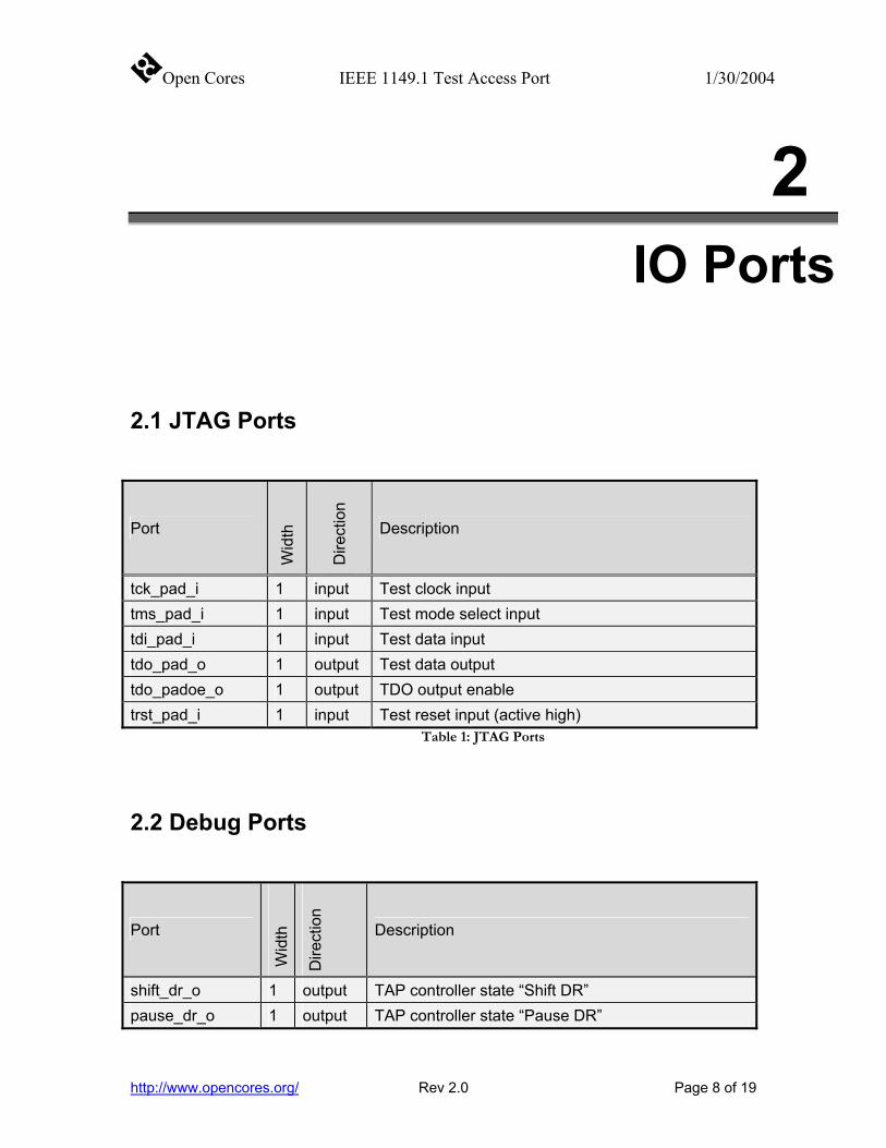
2 IO Ports
2.1 JTAG Ports
Port
Wid
th
Dire
ctio
n
Description
tck_pad_i 1 input Test clock input tms_pad_i 1 input Test mode select input tdi_pad_i 1 input Test data input tdo_pad_o 1 output Test data output tdo_padoe_o 1 output TDO output enable trst_pad_i 1 input Test reset input (active high)
Table 1: JTAG Ports
2.2 Debug Ports
Port
Wid
th
Dire
ctio
n
Description
shift_dr_o 1 output TAP controller state “Shift DR” pause_dr_o 1 output TAP controller state “Pause DR”
Rev 2.0 Page 8 of 19
Open Cores IEEE 1149.1 Test Access Port 1/30/2004
http://www.opencores.org/
Port
Wid
th
Dire
ctio
n
Description
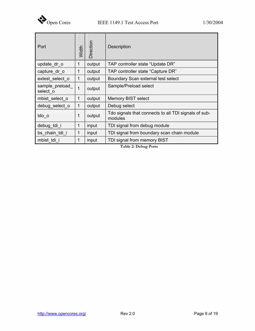
update_dr_o 1 output TAP controller state “Update DR” capture_dr_o 1 output TAP controller state “Capture DR” extest_select_o 1 output Boundary Scan external test select sample_preload_select_o 1 output Sample/Preload select
mbist_select_o 1 output Memory BIST select debug_select_o 1 output Debug select
tdo_o 1 output Tdo signals that connects to all TDI signals of sub-modules
debug_tdi_i 1 input TDI signal from debug module bs_chain_tdi_i 1 input TDI signal from boundary scan chain module mbist_tdi_i 1 input TDI signal from memory BIST
Table 2: Debug Ports
Rev 2.0 Page 9 of 19
Open Cores IEEE 1149.1 Test Access Port 1/30/2004
http://www.opencores.org/
3 Registers
This section specifies all registers in the JTAG Interface.
3.1 Registers List
Name
Wid
th
Acc
ess
Description
IR 4 R/W Instruction Register IDCODE 32 RO IDCODE Register
Table 3: Register List
Rev 2.0 Page 10 of 19
Open Cores IEEE 1149.1 Test Access Port 1/30/2004
http://www.opencores.org/
3.2 IR (Instruction Register)
Bit #
Acc
ess
Description
3:0 R/W INSTR – Instruction 0000 = EXTEST 0001 = SAMPLE_PRELOAD 0010 = IDCODE 1000 = DEBUG 1001 = MBIST 1111 = BYPASS
Table 4: IR Register
Value from this register is always read as 0101b.
3.3 IDCODE register
Bit #
Acc
ess
Description
31:0 RO ID – Identification
Table 5: IDCODE Register
Default valueof the IDCODE register is written in tap_defines.v file.
Rev 2.0 Page 11 of 19
Open Cores IEEE 1149.1 Test Access Port 1/30/2004
4 Operation
This section describes the operation of the JTAG interface, TAP controller, supported instructions, and connection of the sub-modules.
4.2 JTAG Interface and the TAP Controller The JTAG Interface and TAP Controller are fully IEEE Std.1149.1 compliant. JTAG interface consists of six signals:
• tck_pad_i (TCK)
• tms_pad_i (TMS)
• tdi_pad_i (TDI)
• trst_pad_i (TRST)
• tdo_pad_o (TDO)
• tdo_padoe_o
tdo_padoe_o is an enable signal for the TDO pad. tdo_pad_o and tdo_padoe_o should be combined together to the TDO signal on the higher layer.
trst_pad_i is a TRST reset but is active high and not low. This signal should be negated on the higher level. This is done because some pads have an internal inverter.
The following instructions are supported by the TAP (see section for instruction coding):
Table 3: Register List
• EXTEST
• SAMPLE/PRELOAD
• IDCODE
• DEBUG
• MBIST
• BYPASS
All supported instructions are shifted to the instruction register with the LSB bit shifted first.
Supported instructions are described in the following sections.
http://www.opencores.org/ Rev 2.0 Page 12 of 19
Open Cores IEEE 1149.1 Test Access Port 1/30/2004
4.2.1 EXTEST (IR=0000)
The EXTEST instruction connects the boundary scan chain, between the TDI and TDO. During EXTEST instruction, the boundary-scan register is accessed to drive test data off-chip via the boundary outputs and to receive test data in-chip via the boundary inputs. The bit code of this instruction is defined as all zeroes by IEEE Std. 1149.1.
• CaptureDR state: The outputs from the system logic (test vector) are captured.
• ShiftDR state: The captured test vector is shifted out via TDO output while a new test vector is shifted in via the TDI input.
• UpdateDR state: The data shifted in via TDI is applied to Output and Control cells (output pins are driven with 0, 1, or highZ).
4.2.2 SAMPLE/PRELOAD (IR=0001)
The SAMPLE/PRELOAD instruction allows the IC to remain in its functional mode and to select the boundary-scan chain to be connected between TDI and TDO. During this instruction, you can access the boundary-scan chain registers via a data scan operation to take a sample of the functional data entering and leaving the IC. The instruction is also used to preload test data into the boundary-scan register before loading an EXTEST instruction. This instruction should only be used for production tests.
• CaptureDR state: The inputs from the system logic (test vector) are captured.
• ShiftDR state: The captured test vector is shifted out via TDO output while a new test vector is shifted in via TDI input.
• UpdateDR state: No changes.
4.2.3. IDCODE (IR=0010)
The IDCODE instruction allows the IC to remain in its functional mode and selects the device identification register (ID register) to be connected between TDI and TDO. The device identification register is a 32-bit read-only register containing information regarding the IC manufacturer, device type, and version code. Accessing the device identification register does not interfere with the operation of the IC. Also, access to the device identification register should be immediately available via a TAP data-scan operation, after power-up of the IC, or after the TAP has been reset by using the optional trst_pad_i pin or by otherwise moving to the Test-Logic-Reset state.
• CaptureDR state: The ID value is captured from the ID register.
• ShiftDR state: The captured ID value is shifted out via TDO output.
http://www.opencores.org/ Rev 2.0 Page 13 of 19
Open Cores IEEE 1149.1 Test Access Port 1/30/2004
• UpdateDR state: The data shifted in via TDI is ignored (ID is a read-only register).
4.2.4 DEBUG (IR=1000)
The DEBUG instruction is used to enable debugging. In this case debug_tdi_i signal is connected to the TDO. Signal tdo_o must be connected to the TDI signal of the dbg_interface module. For more details see documentation for the dbg_interface available at opencores website.
4.2.5 MBIST (IR=1001)
The MBIST instruction is used for internal memory BIST. When active, mbist_tdi_i is connected to the TDO. Please refer to the MBIST documentation for more details about MBIST.
4.2.6 BYPASS (IR=1111)
The BYPASS instruction keeps the IC in a functional mode and selects that the bypass register will be connected between TDI and TDO. It allows serial data to be transferred through the IC from TDI to TDO without affecting the operation of the IC. The bit code of this instruction is defined as all ones by IEEE Std. 1149.1. Usage of an unimplemented instruction will result in the BYPASS instruction.
• CaptureDR state: A logical 0 is captured in the bypass register.
• ShiftDR state: Input data shifted in via TDI is shifted out via TDO after a one-clock delay.
• UpdateDR state: No changes.
4.3 Scan Chains There are four scan chains connected to the TAP controller:
• ID scan chain
• Debug interface scan chain
• Global boundary scan chain
• Memory BIST scan chain
http://www.opencores.org/ Rev 2.0 Page 14 of 19
Open Cores IEEE 1149.1 Test Access Port 1/30/2004
The last three scan chains are inputs to the TAP controller while ID scan chain is internal. Switching between these four scan chains is done automatically each time a new instruction is shifted into the Instruction Register (see section for more details). Table 4: IR Register
ID scan chain is connected to the TDO when the IDCODE instruction is previously shifted in the IR register. Debug interface scan chain is connected to the TDO when the DEBUG instruction is previously shifted in the IR register. Global BS chain is connected to the TDO when the EXTEST or SAMPLE/PRELOAD instructions are previously shifted in the IR register. Memory BIST scan chain is connected to the TDO when the MBIST instruction is previously shifted in the IR register.
All scan chains are operating at the falling edge of the TCK clock signal.
http://www.opencores.org/ Rev 2.0 Page 15 of 19
Open Cores IEEE 1149.1 Test Access Port 1/30/2004
4.3.1 ID Scan Chain
The ID scan chain is a 32-bit chain used for reading out the internal IDCODE. LSB bit is shifted out first.
4.3.2 Debug Scan Chain
The Debug Interface scan chain is used for interfacing to the debug support (CPU, wishbone…). Please refer to the dbg_interface documentation for more information about this scan chain (length, etc.)
4.3.3 Global BS (Boundary Scan) Chain
This chain allows access to the entire SoC periphery and is used for the boundary scan testing (interconnect test). The chain is automatically selected after the reset.
4.3.4 Memory BIST Scan Chain
This chain allows access to the Memory built-in self test scan chain. MBIST is not part of this project, TAP only has connection ports for it.
http://www.opencores.org/ Rev 2.0 Page 16 of 19
Open Cores IEEE 1149.1 Test Access Port 1/30/2004
5 Architecture
The TAP controller consists of several parts (blocks):
• JTAG interface with the TAP Controller
• Instruction register (described in section on page 11) Table 3: Register List
• Multiplexer that connects one of the scan chains to the TDO.
http://www.opencores.org/ Rev 2.0 Page 17 of 19
Open Cores IEEE 1149.1 Test Access Port 1/30/2004
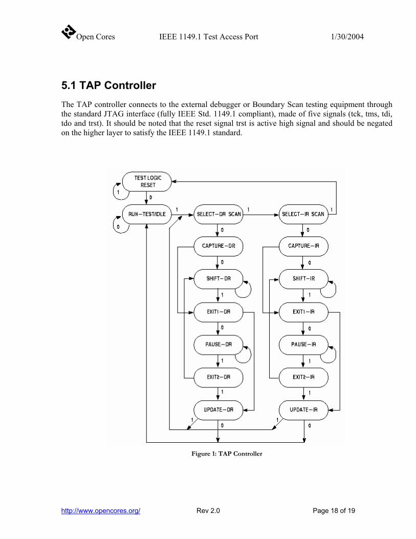
5.1 TAP Controller The TAP controller connects to the external debugger or Boundary Scan testing equipment through the standard JTAG interface (fully IEEE Std. 1149.1 compliant), made of five signals (tck, tms, tdi, tdo and trst). It should be noted that the reset signal trst is active high signal and should be negated on the higher layer to satisfy the IEEE 1149.1 standard.
Figure 1: TAP Controller
http://www.opencores.org/ Rev 2.0 Page 18 of 19
Open Cores IEEE 1149.1 Test Access Port 1/30/2004
http://www.opencores.org/ Rev 2.0 Page 19 of 19
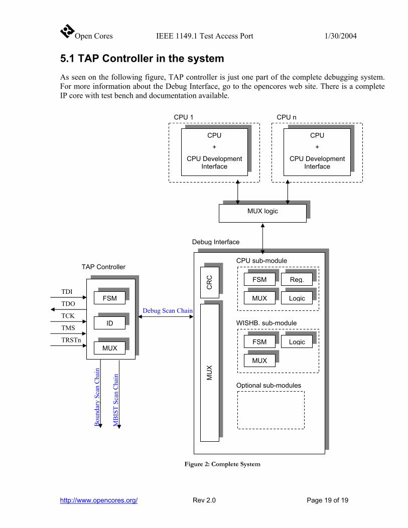
5.1 TAP Controller in the system As seen on the following figure, TAP controller is just one part of the complete debugging system. For more information about the Debug Interface, go to the opencores web site. There is a complete IP core with test bench and documentation available.
Logic
Logic
MUX
FSM
CR
C
Reg.
MUX
FSM
Optional sub-modules
WISHB. sub-module
CPU sub-module
MU
X
ID
FSM
TAP Controller
MUX
MUX logic
CPU 1
CPU
+
CPU Development Interface
CPU n
CPU
+
CPU Development Interface
Debug Interface
TRSTn
TMS
TCK
TDO
TDI
Debug Scan Chain
Bou
ndar
y Sc
an C
hain
MB
IST
Scan
Cha
in
Figure 2: Complete System