Embed Size (px)
Citation preview
Electronic Materials Conference (EMC), 6-25-2009
Improved Migration-Enhanced Epitaxy for Self-Aligned InGaAsEpitaxy for Self Aligned InGaAs
Devices
Mark A. Wistey
University of California, Santa BarbaraNow at University of Notre Dame
U. Singisetti, G. Burek, A. Baraskar, V. Jain, B. Thibault, A. Nelson, E. Arkun, C. Palmstrøm, J. Cagnon, S.
P. McIntyre, B. Shin, E. KimStanford UniversityS. Bank
f
, , g ,Stemmer, A. Gossard, M. RodwellUniversity of California Santa Barbara
University of Texas AustinY.-J. LeeIntel Funding: SRC
Outline: Channels for Future CMOS
•Motivation for Self-Aligned RegrowthF t G A i Fl d MEE•Facets, Gaps, Arsenic Flux and MEE
•Si doping and MEE•Scalable III-V MOSFETs•The Shape of Things to Come•The Shape of Things to Come
2Wistey, EMC 2009
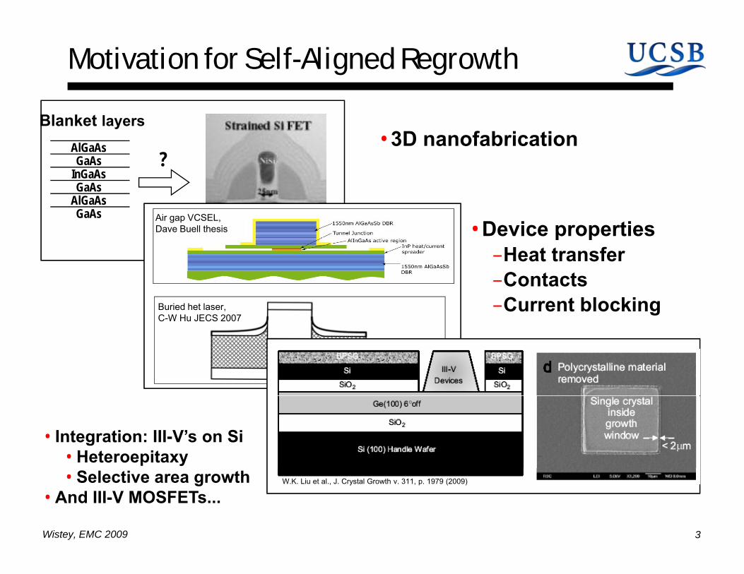
Motivation for Self-Aligned Regrowth
• 3D nanofabricationAlGaAsGaAs
InGaAs
Blanket layers
?
Qi Xinag, ECS 2004, AMD
GaAsAlGaAsGaAs
• Device propertiesHeat transfer
Air gap VCSEL,Dave Buell thesis
–Heat transfer–Contacts–Current blockingBuried het laser,
C-W Hu JECS 2007
• Integration: III-V’s on Si• Heteroepitaxy
3Wistey, EMC 2009
W.K. Liu et al., J. Crystal Growth v. 311, p. 1979 (2009)• Selective area growth• And III-V MOSFETs...
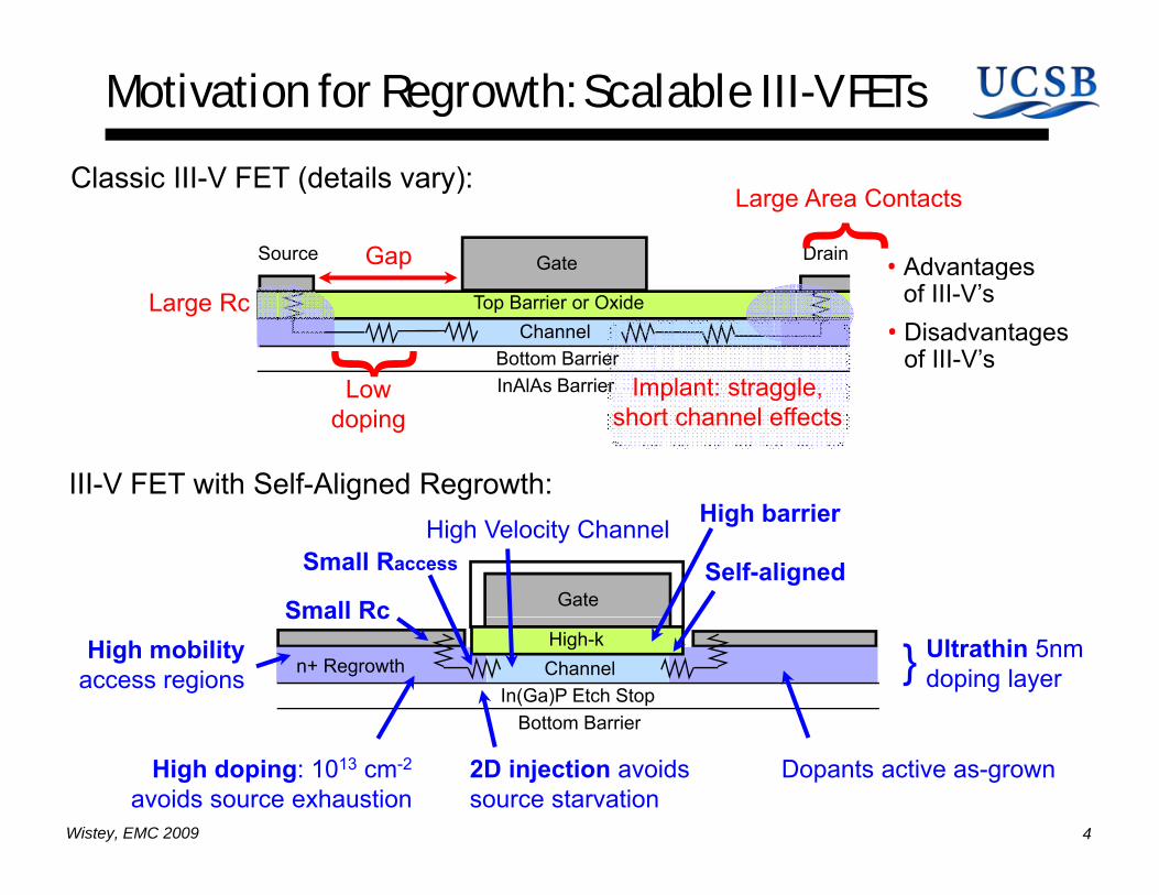
Motivation for Regrowth: Scalable III-V FETs
Classic III-V FET (details vary):
GateGapSource Drain
Large Area Contacts
• Advantages
ChannelBottom BarrierInAlAs Barrier
Top Barrier or Oxide
Low
Large Rcg
of III-V’s• Disadvantages
of III-V’sImplant: straggleInAlAs BarrierLow
doping
III-V FET with Self-Aligned Regrowth:
Implant: straggle,short channel effects
Hi h b i
Gate
High Velocity ChannelSmall Raccess
Small RcSelf-aligned
High barrier
ChannelIn(Ga)P Etch Stop
Bottom Barrier
High-kn+ Regrowth
Small RcHigh mobility
access regionsUltrathin 5nm doping layer
4Wistey, EMC 2009
High doping: 1013 cm-2
avoids source exhaustion 2D injection avoids source starvation
Dopants active as-grown
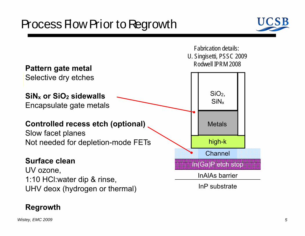
Process Flow Prior to Regrowth
Pattern gate metal
Fabrication details: U. Singisetti, PSSC 2009
Rodwell IPRM 2008
Selective dry etches
SiNx or SiO2 sidewallsE l t t t l
SiO2,SiNxEncapsulate gate metals
Controlled recess etch (optional)Slow facet planes
Metals
SiNx
Slow facet planesNot needed for depletion-mode FETs
Surface clean I (G )P t h t
high-k
ChannelSurface cleanUV ozone, 1:10 HCl:water dip & rinse, UHV deox (hydrogen or thermal)
In(Ga)P etch stop
InAlAs barrierInP substrate
5Wistey, EMC 2009
( y g )
Regrowth
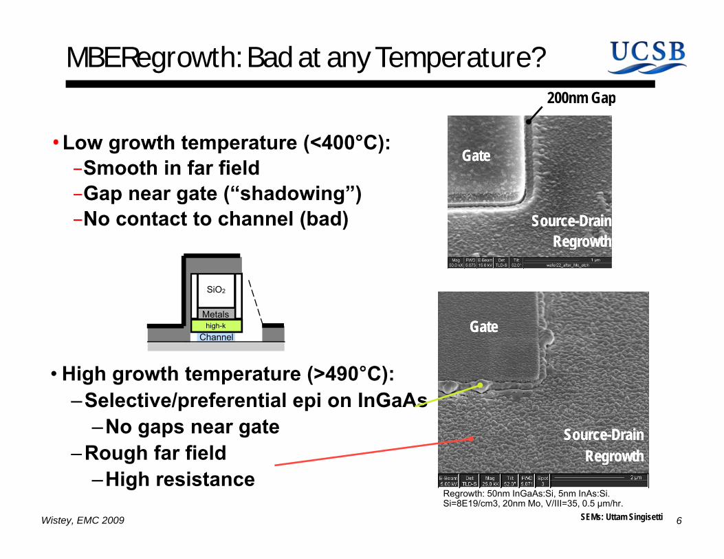
MBE Regrowth: Bad at any Temperature?200nm Gap
• Low growth temperature (<400°C):–Smooth in far field GateGate
p
Smooth in far field–Gap near gate (“shadowing”)–No contact to channel (bad) Source-Drain
RegrowthSource-Drain
RegrowthRegrowthRegrowth
Metals
SiO2
Metals
Channelhigh-k GateGate
• High growth temperature (>490°C):
Source-DrainRegrowth
Source-DrainRegrowth
–Selective/preferential epi on InGaAs–No gaps near gate
–Rough far field
6Wistey, EMC 2009 SEMs: Uttam Singisetti
RegrowthRegrowth
Regrowth: 50nm InGaAs:Si, 5nm InAs:Si. Si=8E19/cm3, 20nm Mo, V/III=35, 0.5 µm/hr.
Rough far field –High resistance
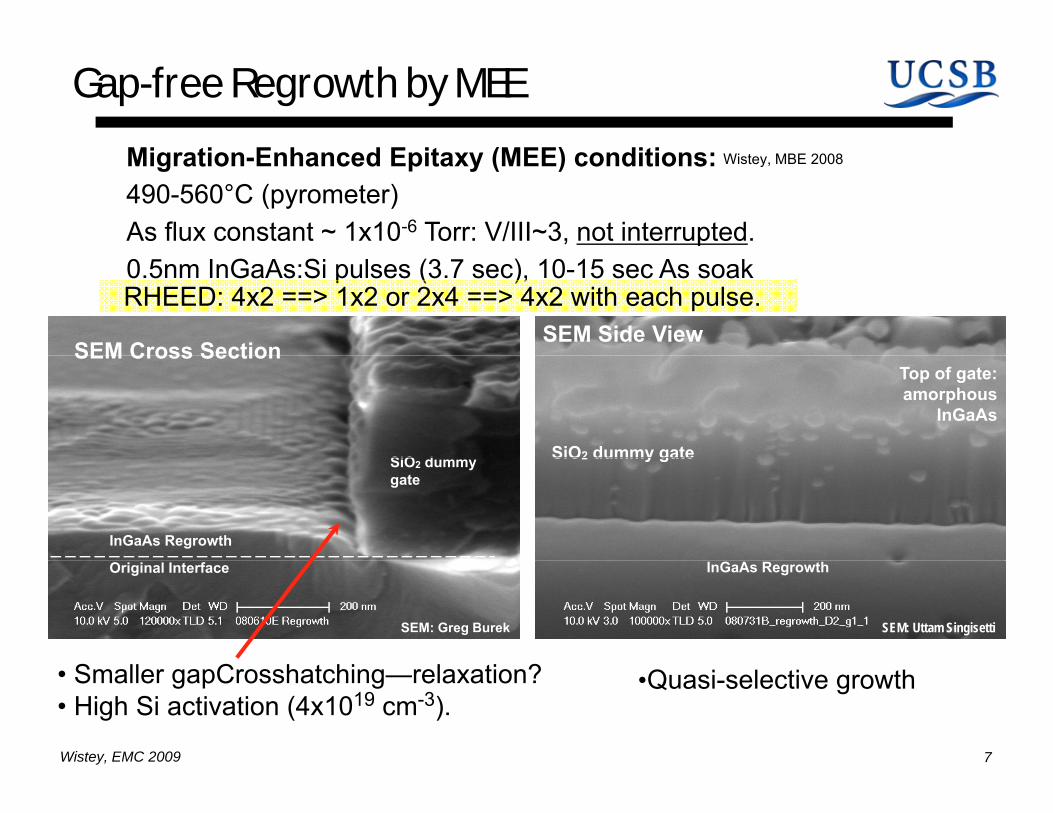
Gap-free Regrowth by MEE
Mi ti E h d E it (MEE) ditiMigration-Enhanced Epitaxy (MEE) conditions:490-560°C (pyrometer)As flux constant ~ 1x10⁻⁶ Torr: V/III~3, not interrupted.
Wistey, MBE 2008
0.5nm InGaAs:Si pulses (3.7 sec), 10-15 sec As soak
SEM Cross SectionSEM Side View
RHEED: 4x2 ==> 1x2 or 2x4 ==> 4x2 with each pulse.
SiO d
SEM Cross Section
SiO2 dummy gate
Top of gate: amorphous
InGaAs
InGaAs Regrowth
SiO2 dummy gate
SiO2 dummy gate
Original Interface
SEM: Greg Burek SEM: Uttam Singisetti
InGaAs Regrowth
7Wistey, EMC 2009
• Smaller gapCrosshatching—relaxation?• High Si activation (4x1019 cm-3).
•Quasi-selective growth
490C460C
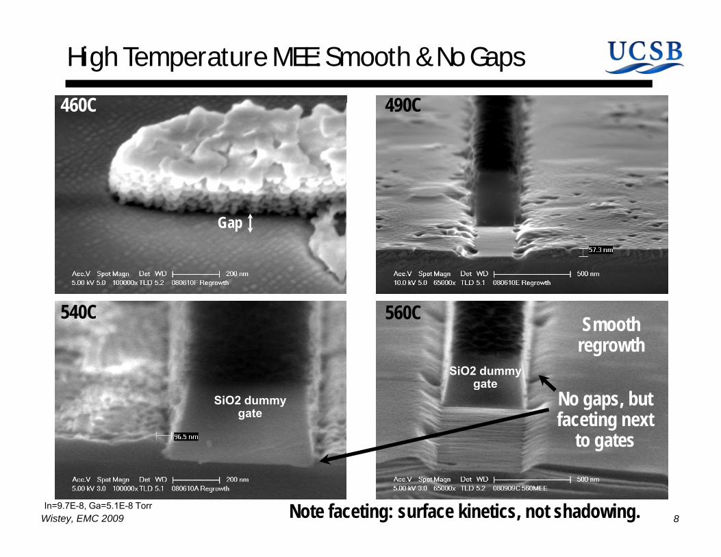
High Temperature MEE: Smooth & No Gaps
490C460C
Gap
560C540C 560C
SiO2 dummy gate
540C Smooth regrowth
SiO2 dummy gate
gateNo gaps, but faceting next
to gates
8Wistey, EMC 2009 Note faceting: surface kinetics, not shadowing.In=9.7E-8, Ga=5.1E-8 Torr
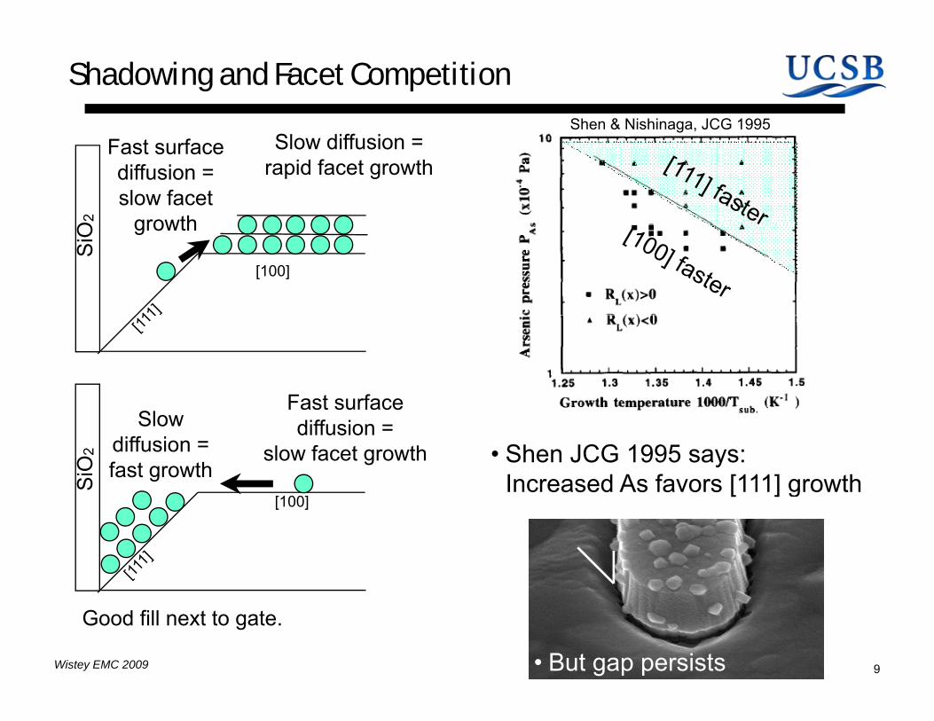
Shadowing and Facet CompetitionShen & Nishinaga, JCG 1995
Fast surface diffusion = slow facet
growth
Slow diffusion = rapid facet growth
O2
[100]
growth
SiO
Fast surface
• Shen JCG 1995 says:Increased As favors [111] growth
[100]
Slow diffusion =fast growth
Fast surface diffusion =
slow facet growth
SiO
2
g[100]
Wistey EMC 2009 9
Good fill next to gate.
• But gap persists
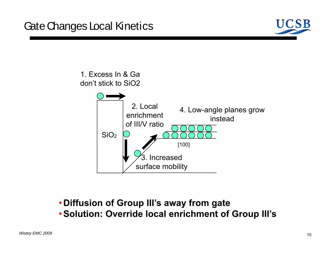
Gate Changes Local Kinetics
1. Excess In & Ga
2. Local 4 Low-angle planes grow
don’t stick to SiO2
[100]
enrichment of III/V ratio
4. Low-angle planes grow instead
SiO2
[100]
3. Increased surface mobility
• Diffusion of Group III’s away from gate
Wistey EMC 2009 10
p y g• Solution: Override local enrichment of Group III’s
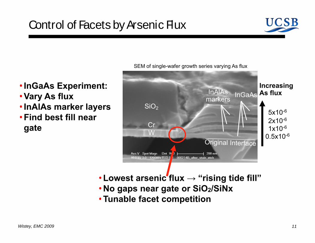
Control of Facets by Arsenic Flux
SEM of single-wafer growth series varying As flux
SiO
Increasing As fluxInAlAs
markers InGaAs• InGaAs Experiment:• Vary As flux• InAlAs marker layers SiO2
WCr
• InAlAs marker layers• Find best fill near gate
0 5x10-61x10-62x10-65x10-6
0.5x10
• Lowest arsenic flux → “rising tide fill”• No gaps near gate or SiO2/SiNx• Tunable facet competition
11Wistey, EMC 2009
• Tunable facet competition
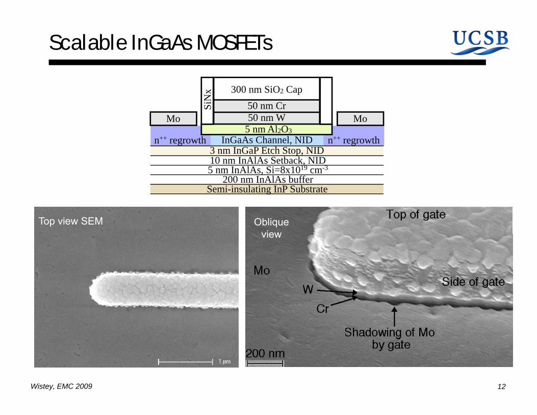
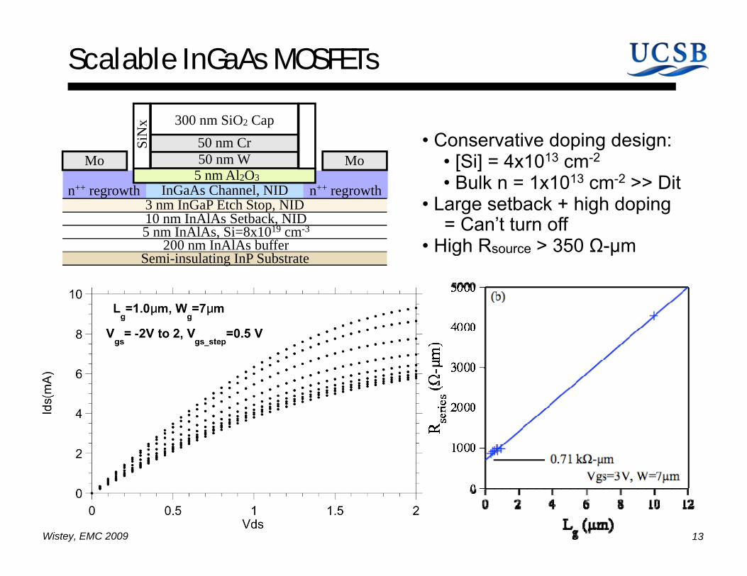
Scalable InGaAs MOSFETs
5 nm Al2O3
50 nm W
300 nm SiO2 Cap
SiN
x
50 nm CrMo Mo
InGaAs Channel, NID
10 nm InAlAs Setback, NID
5 nm Al2O3
5 nm InAlAs, Si=8x1019 cm-3
200 nm InAlAs buffer
n++ regrowthn++ regrowth3 nm InGaP Etch Stop, NID
Semi-insulating InP Substrate200 nm InAlAs buffer
Top view SEM Obliqueviewview
12Wistey, EMC 2009
Scalable InGaAs MOSFETs
5 nm Al2O3
50 nm W
300 nm SiO2 CapSi
Nx
50 nm CrMo Mo
• Conservative doping design:• [Si] = 4x1013 cm-2
Bulk n 1x1013 cm-2 >> DitInGaAs Channel, NID
10 nm InAlAs Setback, NID
5 nm Al2O3
5 nm InAlAs, Si=8x1019 cm-3
200 nm InAlAs buffer
n++ regrowthn++ regrowth3 nm InGaP Etch Stop, NID
• Bulk n = 1x1013 cm-2 >> Dit• Large setback + high doping
= Can’t turn off• High Rsource > 350 Ω-µm
Semi-insulating InP SubstrateHigh Rsource 350 Ω µm
13Wistey, EMC 2009
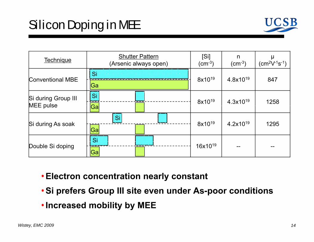
Silicon Doping in MEE
Technique Shutter Pattern(Arsenic always open)
[Si] (cm-3)
n (cm-3)
µ (cm2V-1s-1)
SiConventional MBE 8x10¹⁹ 4.8x10¹⁹ 847
Si during Group III MEE pulse 8x10¹⁹ 4.3x10¹⁹ 1258
Ga
Si
Ga
SiMEE pulse
Si during As soak 8x10¹⁹ 4.2x10¹⁹ 1295
Ga
Ga
Si
Double Si doping 16x1019 -- --Ga
Si
• Electron concentration nearly constant• Si prefers Group III site even under As-poor conditions
14Wistey, EMC 2009
• Increased mobility by MEE
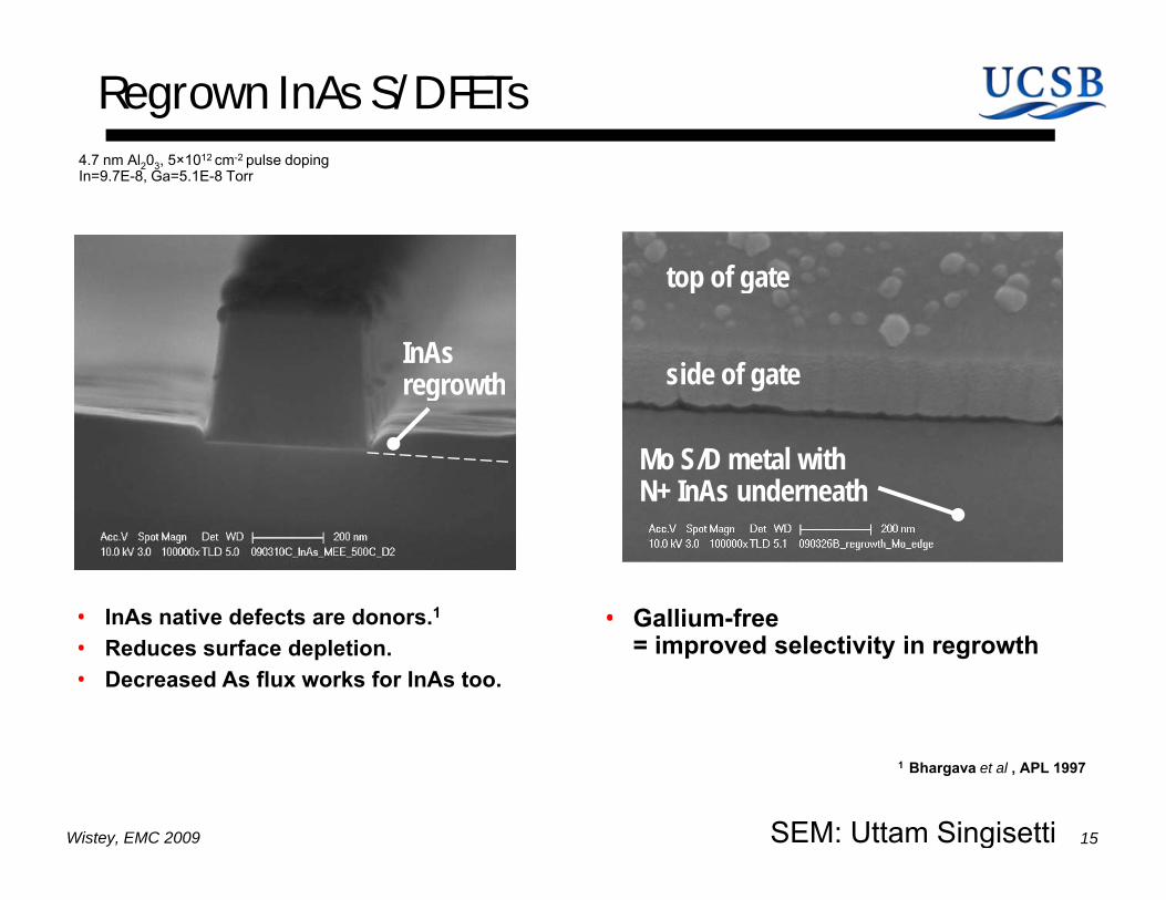
Regrown InAs S/D FETs4.7 nm Al203, 5×1012 cm-2 pulse doping
top of gate
2 3, p p gIn=9.7E-8, Ga=5.1E-8 Torr
side of gate
top of gate
InAsregrowth
Mo S/D metal with N+ InAs underneath
regrowth
• Gallium-free• InAs native defects are donors 1 • Gallium-free= improved selectivity in regrowth
InAs native defects are donors.• Reduces surface depletion. • Decreased As flux works for InAs too.
15Wistey, EMC 2009 SEM: Uttam Singisetti
1 Bhargava et al , APL 1997
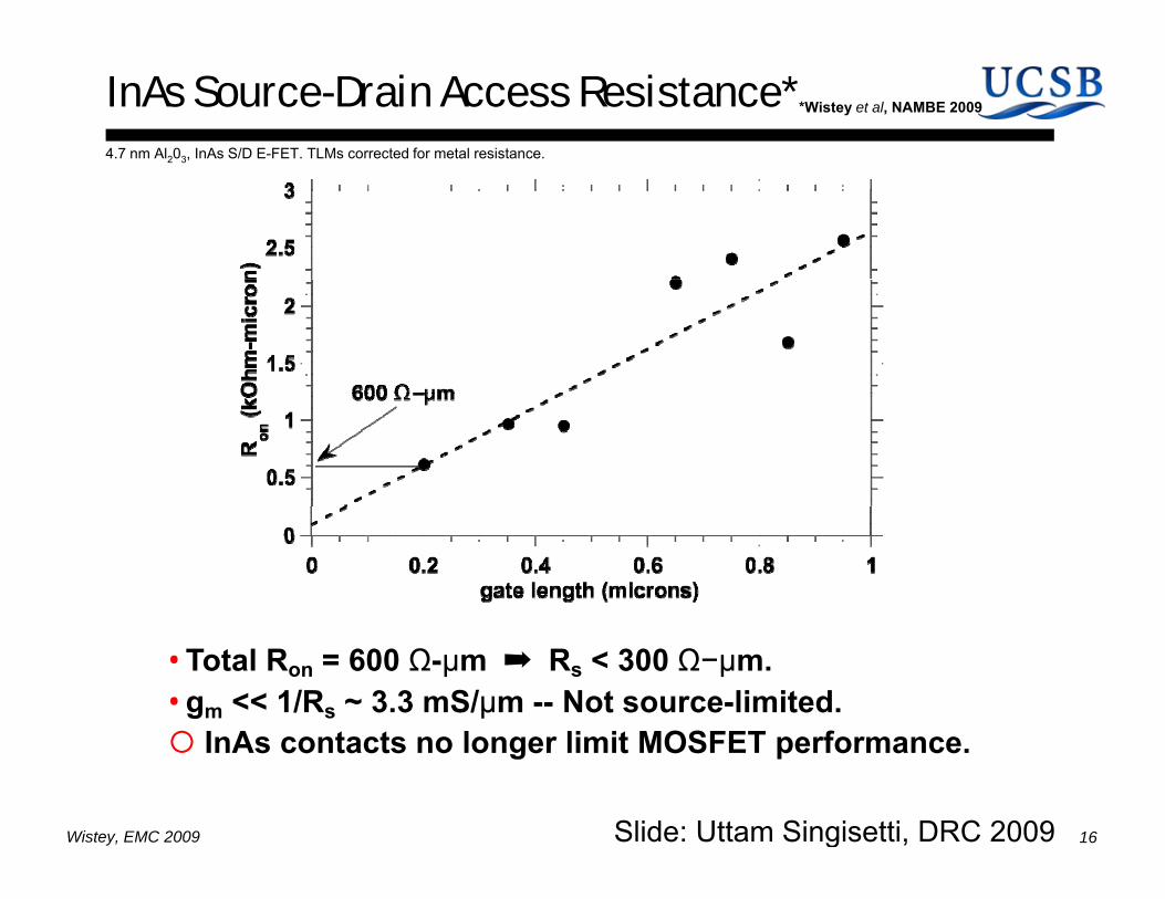
InAs Source-Drain Access Resistance* *Wistey et al, NAMBE 2009
4.7 nm Al203, InAs S/D E-FET. TLMs corrected for metal resistance.
• Total Ron = 600 Ω-μm Rs < 300 Ω−μm.• gm << 1/Rs ~ 3.3 mS/μm -- Not source-limited.
I A t t l li it MOSFET f
16Wistey, EMC 2009 Slide: Uttam Singisetti, DRC 2009
InAs contacts no longer limit MOSFET performance.
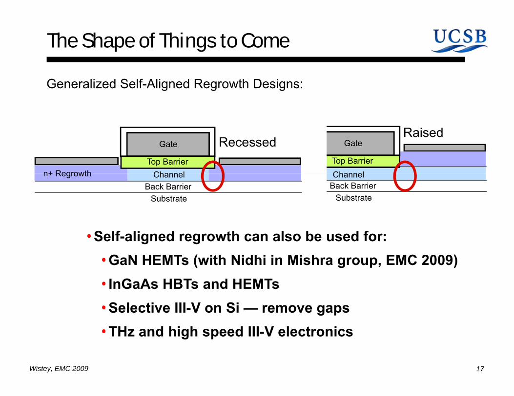
The Shape of Things to Come
Generalized Self-Aligned Regrowth Designs:
ChannelTop Barrier
Gate
n+ RegrowthTop Barrier
GateRecessedRaised
ChannelChannelBack Barrier
Substrate
n+ RegrowthBack Barrier
Substrate
Channel
• Self-aligned regrowth can also be used for:• GaN HEMTs (with Nidhi in Mishra group, EMC 2009)• InGaAs HBTs and HEMTs• Selective III-V on Si — remove gaps
17Wistey, EMC 2009
• THz and high speed III-V electronics
Conclusions
• Reducing As flux improves filling near gate• Self-aligned regrowth: a roadmap for scalable III-V FETs
–Provides III-V’s with a salicide equivalent–Can improve GaN and GaAs FETs too
Silicon doping imper io s to MEE techniq e• Silicon doping impervious to MEE technique• InAs regrown contacts improve InGaAs MOSFETs...
Not limited by source resistance @ 1 mA/µm–Not limited by source resistance @ 1 mA/µm–Comparable to other III-V FETs... but now scalable
18Wistey, EMC 2009
Acknowledgements
• Rodwell & Gossard Groups (UCSB): Uttam Singisetti, Greg Burek, Ashish Baraskar, Vibhor Jain...
• McIntyre Group (Stanford): Eunji Kim Byungha Shin• McIntyre Group (Stanford): Eunji Kim, Byungha Shin, Paul McIntyre
• Stemmer Group (UCSB): Joël Cagnon, Susanne StStemmer
• Palmstrøm Group (UCSB): Erdem Arkun, Chris Palmstrøm
• SRC/GRC funding• UCSB Nanofab: Brian Thibeault, NSF
19Wistey, EMC 2009


![Wide-Bandga 16.Wide-BandgapII-VISemiconductors ... · molecular-beam epitaxy (MBE) [16.3], metalorganic molecular-beam epitaxy (MOMBE) [16.4] and atomic-layer epitaxy (ALE) [16.5]](https://img.pdfslide.net/doc/110x75/5e1f371b74bffa7fb71fc624/wide-bandga-16wide-bandgapii-visemiconductors-molecular-beam-epitaxy-mbe.jpg)